


Abstract
With the rapid development of DC grids, resonant DC circuit breakers (RDCBs) have become critical for fault isolation. However, existing RDCBs often suffer from severe energy mismatches, and components, including mechanical switches, resonant capacitors, and power electronic devices, suffer from excessive internal overvoltage during the current interruption process. To address these issues, a novel RDCB with a capacitor self-charging current excitation source (CES) is proposed in this paper. First, by controlling the charging process of CES by the fault current, the injected energy is matched with the commutation requirements, significantly reducing the transient recovery voltage (TRV) applied to the mechanical switch. Second, to suppress the voltage applied to the resonant capacitor, a metal oxide arrestor (MOA) should be connected directly in parallel with the resonant capacitor, avoiding overvoltage caused by the internal oscillation between the resonant inductance and the resonant capacitor. Furthermore, an anti-parallel magnetic core is designed for CES, ensuring dynamic current sharing among parallel IGBTs while maintaining a zero-inductance characteristic externally. Simulation results verify that the proposed RDCB reduces the peak TRV by at least 64% compared with existing RDCBs. Furthermore, the effectiveness of the proposed overvoltage suppression methods is validated, significantly improving the interrupting reliability.
1. Introduction
With the rapid development of renewable energy integration and flexible DC grids, DC circuit breakers (DCCBs) are critical for maintaining system security [1,2,3,4]. Nevertheless, mechanical DCCB and hybrid DCCB face limitations of high cost and complexity, hindering their widespread application in large-scale multi-port DC grids [5,6,7,8]. To address these challenges, resonant DCCBs (RDCBs) have emerged as a promising research direction, providing a highly economical and efficient solution for DC fault isolation [9,10].
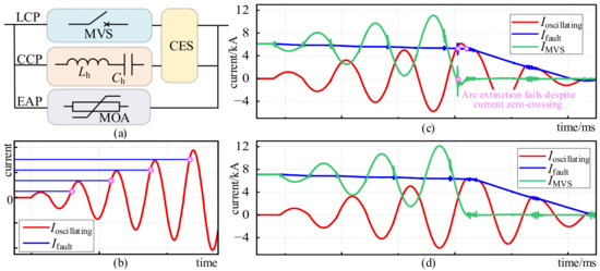
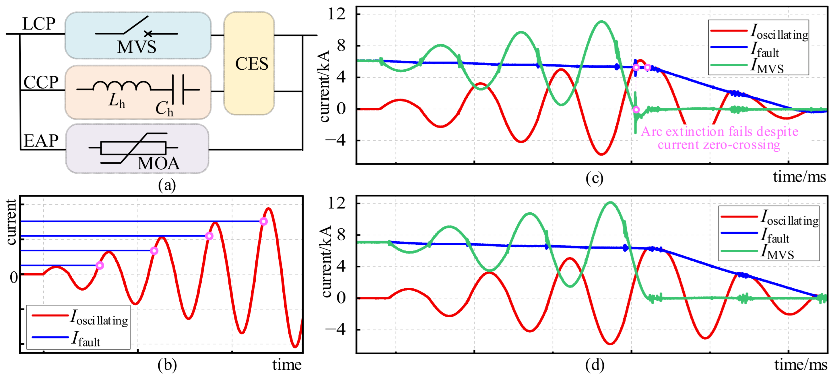
As shown in Figure 1a, the RDCB topology comprises three functional paths: the load current path (LCP), the current commutation path (CCP), and the energy absorption path (EAP) [11,12]. The LCP uses an ultra-fast mechanical vacuum switch (MVS) to handle the steady-state load current. Within the CCP, a resonant capacitor (Ch) and inductor (Lh) form an oscillatory circuit, generating a high-frequency current that counteracts the fault current, thereby forcing the MVS current to zero. Residual energy is dissipated via the metal oxide arrester (MOA) in the EAP. The current excitation source (CES) is the key element for realizing the current commutation from LCP to CCP. Upon fault detection, energy is transferred from the CES to LC components (Ch and Lh), generating a high-frequency oscillating current in the CCP that opposes the fault current. This interaction forces the MVS current to zero, creating an artificial current zero-crossing for interruption. Although the CES is also implemented using power electronic devices, it is capable of generating a large current with low voltage stress on the CES, significantly reducing the number of components required.
Figure 1.
Overview of arc extinction difficulty. (a) topology of RDCB; (b) specific points where arc extinction is difficult; (c) fault current of 6 kA; (d) fault current of 7 kA.
However, existing RDCBs still face arc extinction challenges under wide-range fault current conditions. The switching stress of MVS is primarily determined by the pre-arcing di/dt and the post-arcing du/dt, imposing stringent requirements on the energy injected by the CES. Due to the uncontrolled energy of CES in existing topologies, it is difficult to achieve adaptive adjustment in response to the actual fault current. The surplus energy injected by the CES exacerbates the interruption stress on MVS, making it difficult to match all operating conditions, especially under the special operating condition shown in Figure 1b, where transient interruption voltage (TRV) becomes excessively high, resulting in the most severe arc extinction condition. Experimental results indicate that when the fault current is 6 kA, excessive surplus energy leads to extremely high TRV, causing the arc to fail to extinguish despite current zero-crossing, as shown in Figure 1c. Conversely, under the 7 kA condition, although the fault current is larger, the oscillating current counteracts the fault current more effectively, resulting in better energy matching. And the reliable interruption is achieved, as shown in Figure 1d. The uncontrollable injection energy of CES in existing RDCBs prevents adaptive response to fault current variations, severely limiting its interruption performance under complex operating conditions.
Meanwhile, during the micro-transient process of forced high-frequency commutation and intense energy injection, the extremely high rate of current change subjects the internal components to severe overvoltage and overcurrent shocks. However, existing research predominantly focuses on system-level interruption mechanisms and macro-topology optimization. There is a notable lack of in-depth quantitative analysis regarding the electrical stresses on internal modular components and their suppression methods. Regarding overvoltage suppression, MOAs are widely employed in parallel to protect Ch. Existing topologies typically connect the MOA across the entire Ch-Lh loop [13,14,15]. However, this configuration neglects the effect of Lh. Under high-frequency excitation, this oversight allows trapped energy to recirculate within the Ch-Lh loop, triggering local resonances that elevate the voltage across far beyond the external clamping level, leading to insulation failure. Regarding current balancing, the low-voltage CES requires parallel IGBTs to meet high short-circuit current. However, due to variations in on-state voltage drops and non-simultaneous switching actions, severe dynamic current imbalance is easily induced among the parallel branches [15,16]. Although active control methods based on temperature compensation, gate timing adjustment, or distributed active triggering have been proposed [17,18,19], these methods mainly aim to eliminate switching inconsistency and often have limited effectiveness for existing device differences. Moreover, under complex control schemes, significant induced voltage spikes are readily generated in the external circuit. This distortion of the output square wave subsequently suppresses the normal growth of the resonant current.
To address these issues, a novel RDCB with a self-charging CES is proposed to ensure the reliable arc extinction of MVS caused by excessive TRV. As the charging process of CES is controllable by the fault current, the injected energy is always matched with the current commutation requirements, significantly reducing TRV below 4.5 kV (reducing it by at least 64%) applied on MVS. It effectively suppresses the overvoltage, ensures reliable interruption, and provides comprehensive overvoltage suppression. The rest of this article is organized as follows: an overview of the RDCB and the principle of TRV generation is provided in Section 2. The topology and characteristics of the proposed RDCB with capacitor self-charging CES are presented in Section 3. The overvoltage stress and suppression for Ch and parallel IGBTs of the proposed RDCB are analyzed in Section 4. A simulation model based on PSCAD is developed to verify the effectiveness of the proposed RDCB and overvoltage suppression methods in Section 5. Finally, a comprehensive comparison regarding economic cost, TRV, and pre-charging requirements between the proposed CES and existing CES is provided in Section 5.
2. Overview of RDCB and the Generation of TRV
2.1. Overview of RDCB
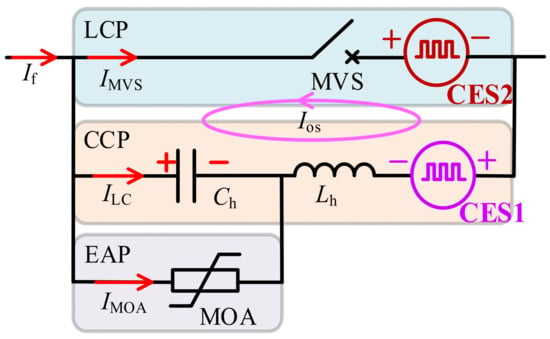
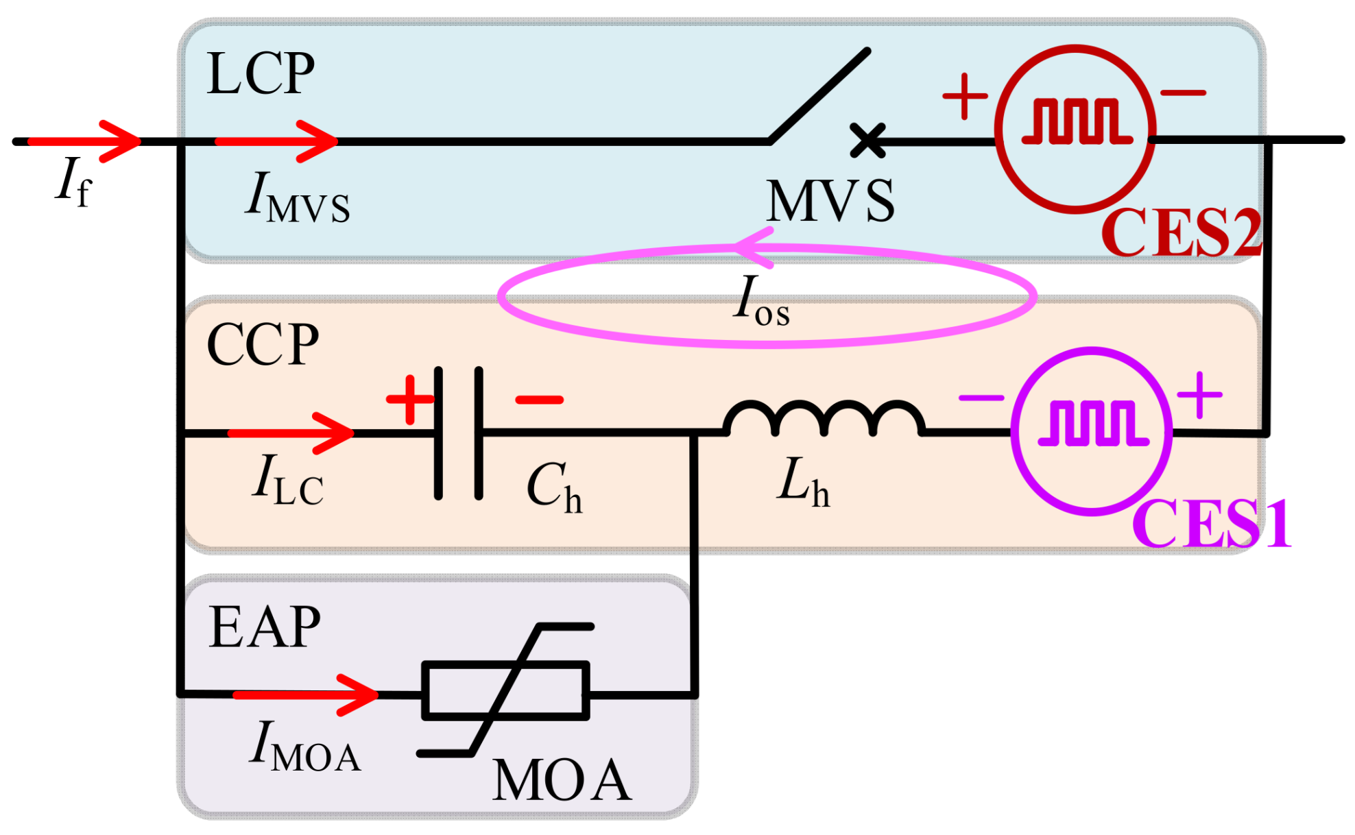
The structure of the RDCB is shown in Figure 2. Under normal operating conditions, the MVS is closed, and the current (If) flows through LCP.
Figure 2.
Structure of RDCB.
During the interruption process, the MVS is opened, and a stable square-wave voltage is generated by CES to continuously charge the LC components in the CCP, thereby exciting the resonant current Ios. The current through LCP (IMVS) is the fault current (If) minus Ios. Once the amplitude of Ios exceeds If, the arc in MVS is extinguished, resulting in complete current commutation from LCP to CCP and arc extinction in the MVS. Subsequently, Ch continues to be charged by If until the voltage on Ch (UCh) reaches the reference voltage of the MOA. If is then commutated to the EAP and gradually attenuated to zero through the energy dissipation of MOA.
Consequently, the key for RDCB to achieve current commutation is that CES continuously injects energy into the LC components during the commutation process. This energy alternates between Lh and Ch, manifesting externally as an oscillating current and voltage with progressively increasing amplitudes.
2.2. Type of CES
Existing CES for RDCB can be categorized into two types: the pre-charged capacitor type and the MOA switching type.
2.2.1. Pre-Charged Capacitor CES and Its External Characteristic
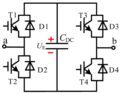
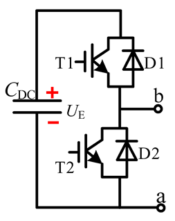
The pre-charged capacitor type CES is generally located in CCP, as shown by CES1 in Figure 2 [20,21,22]. It consists of a bridge circuit in conjunction with a pre-charged capacitor, as listed in Table 1. The pre-charged capacitor serves as a voltage source, using the bridge topology to control its discharge polarity. Upon fault occurrence, the direction of output voltage of the CES (UCES) is controlled to remain consistent with the direction of Ios, thereby realizing the continuous discharge of Ch. As a result, UCh rises continuously, forcing Ios to increase progressively and providing a reliable current zero-crossing point for MVS.
Table 1.
The structure of the pre-charging capacitor type CES, and its output voltage.
Taking a full-bridge IGBT circuit as an example, when Ios is counterclockwise, T2/T3 are controlled to turn on, and Ios flows through a-T2-CDC-T3-b. The CES outputs a positive pre-charged capacitor voltage, UCES = Uba = UE. When Ios is clockwise, T1/T4 are controlled to turn on, and Ios flows through b-T4-CDC-T1-a. The CES outputs a negative pre-charged capacitor voltage, UCES = Uba = −UE.
For the half-bridge circuit configuration, when Ios is counterclockwise, T1 is turned on, and Ios flows through a-CDC-T1-b. The CES outputs a positive pre-charged capacitor voltage, UCES = Uba = UE. However, when Ios is clockwise, T2 is turned on, and Ios flows through b-T2-a. The CES outputs zero voltage, UCES = Uba = 0.
2.2.2. MOA Switching CES and Its External Characteristic
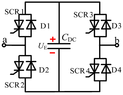
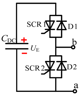
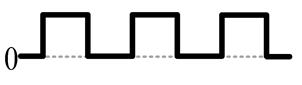
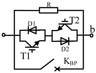
For the MOA switching type, CES is generally located in LCP, as shown by CES2 in Figure 2 [23,24,25]. This structure replaces the pre-charged capacitor in the full-bridge topology with an MOV, which effectively acts as a voltage source by using its resistance effect to generate a voltage drop, leading to two configurations: the MOA switching type and the ordinary resistor switching type, as listed in Table 2. When current flows through the resistor, a resistive voltage drop appears across its terminals; when no current flows through the resistor, the voltage is zero. By controlling the turn-on and turn-off states of the power electronic switches paralleled with the MOA, the CES is controlled to output a positive voltage when current is positive, and zero voltage when current is negative, thereby enabling continuous discharge of LC components.
Table 2.
The structure of the MOV switching type CES and its output voltage.
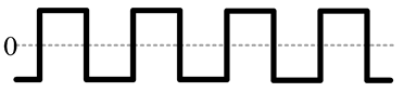
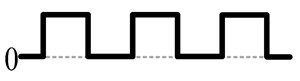
Due to the nonlinear characteristics of the MOA, the terminal voltage is clamped at its residual voltage when conducting current. Therefore, by controlling the switching operation of MOA, a controllable square-wave voltage can be generated. For an ordinary resistor, the terminal voltage depends on the magnitude of the current flowing through it. Consequently, when the current is positive, UCES is a sinusoidal waveform superimposed with a positive DC bias voltage.
2.2.3. Energy Injection Principle of the CES
For the MOA switching CES, the energy absorbed by the MOA after a fault occurs is given by (1).
Consequently, the energy injected by CES into LC components is the energy injected by the system into the CES minus the energy absorbed by the MOA in CES, as (2).
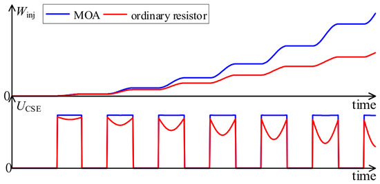
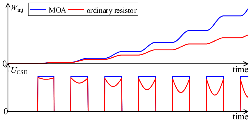
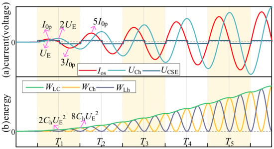
Given the voltage withstand limitation of the device, the square-wave voltage can provide a constant voltage during the conduction period, making the energy injected in each cycle essentially constant, thereby maximizing the energy injection growth, as shown by the blue curve in Figure 3. In contrast, for the ordinary resistor, the voltage is a sinusoidal waveform superimposed with a positive DC bias voltage, causing the energy injected to be limited by the voltage, resulting in slow energy growth. Therefore, to maximize commutation efficiency, UCES should be a square-wave voltage as much as possible.
Figure 3.
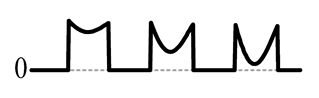
Schematic of energy and voltage characteristics for different UCES.
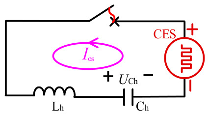
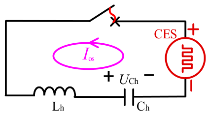
Regardless of the CES type, the circuit schematic diagram of the energy injection into LC components is shown in Figure 4.
Figure 4.
Circuit schematic diagram of the energy injection.
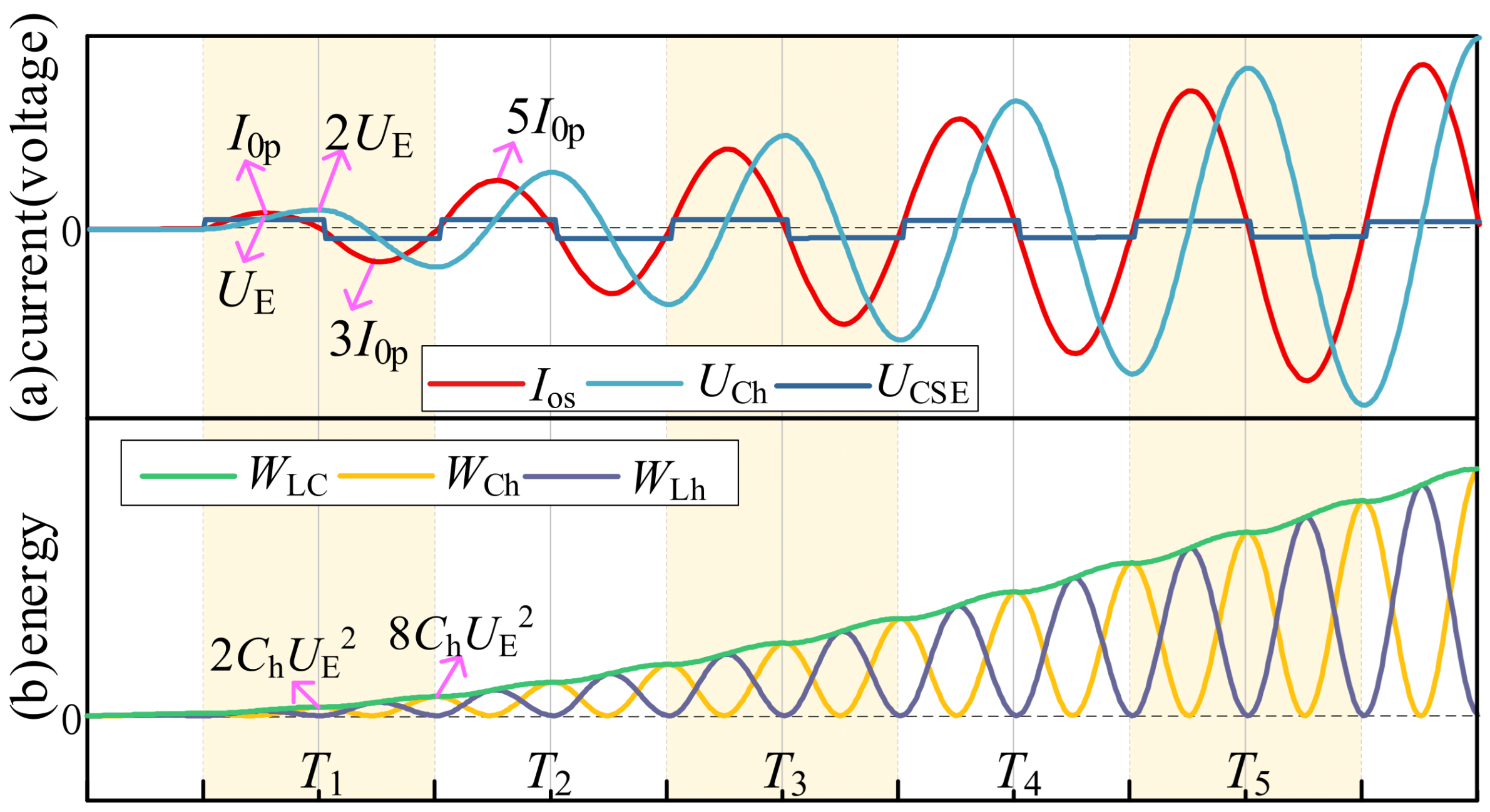
Assuming no energy is dissipated by stray resistances in the loop, a schematic diagram of the electrical quantity variations in the energy injection loop is shown in Figure 5.
Figure 5.
Schematic diagram of the electrical quantity variations during the energy injection process.
As shown in Figure 5, initially, Ios is zero, and no energy is stored in Ch and Lh. During the first half-cycle (positive half-wave of Ios), since Ios and UCES are in the same direction, the CES injects energy into the LC components. Ios increases gradually, charging Ch, as (3).
According to (3), UCh is equal to UE when Ios reaches its peak value. Charging of Ch continues until Ios falls to zero, at which point UCh rises to 2UE, and the total energy injected into LC components (Winj) is 2ChUE2.
For the pre-charged capacitor CES, UCES is controlled to be in the same direction as Ios. During the negative half-wave, UCES is also negative, and the energy injection principle is the same as that for the positive half-wave. By the end of this period, UCh amplitude rises to 4UE, and Winj increases to 8ChUE2. Subsequently, in each subsequent cycle, UCh increases by 4UE, and Winj increases by 8(2n − 1)ChUE2 (where n is the cycle number).
For the MOA switching CES, only positive or zero voltage is output by the CES, and the positive or negative of Ios is controlled to match accordingly. During the negative half-wave, UCES is zero, resulting in no energy output. UCh remains unchanged, and Winj is maintained at 2ChUE2. Thereafter, UCh increases by 2UE, and Winj increases by 2(2n − 1)ChUE2 (where n is the cycle number).
In summary, although the operating modes of the two CES are different, their square-wave output voltages are essentially constant. Therefore, Winj increases gradually in each cycle.
2.2.4. Generation Mechanism of TRV Across MVS and Re-Strikes Risks
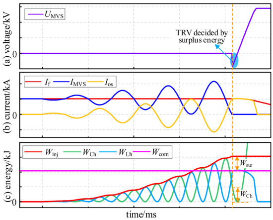
A typical process of the existing RDCB is shown in Figure 6. Within microseconds after the current zero-crossing, MVS contacts gradually separate, forming an equivalent gap capacitance (Cg) between the moving and stationary contact plates. When Winj exceeds the commutation requirement (Wcom), surplus energy (Wsur) cannot be dissipated instantaneously and is transferred to Cg. Since Cg is typically very small (tens to hundreds of pF), even a small Wsur results in a sharp rise in the voltage across MVS, generating the transient recovery voltage (TRV), as shown by the blue-shaded region in Figure 6a. In this paper, TRV is defined as the first voltage peak across the MVS immediately after the current zero-crossing. This definition is adopted because the first peak of TRV is the most critical factor affecting the arc extinction and re-strikes risks of MVS. If the first peak exceeds the dielectric recovery strength of the MVS, re-strikes will occur immediately.
Figure 6.
Variation in electrical quantities during the interruption process: (a) voltage; (b) current; (c) energy.
During the resonance process, the total energy of LC components is determined by the energy injected by the CES, which is jointly composed of the energy stored in Ch and Lh. When the amplitude of Ios reaches If and the current zero-crossing is achieved, the energy required for the commutation process corresponds only to the energy stored in Lh. At this point, the energy stored in Ch constitutes Wsur, as shown in Figure 6c.
When Winj matches Wcom within a given cycle, the IMVS current zero-crossing occurs at the point where UCh is zero, resulting in a first TRV peak of zero. When Winj exceeds Wcom, the first peak of TRV is determined by Wsur. Moreover, the larger Wsur, the higher TRV, and the greater the arc extinction pressure.
The primary cause of TRV across MVS is the imbalance between Winj and Wcom. Since Winj, injected by existing CES, increases gradually in each cycle, this imbalance cannot be avoided due to the uncontrolled injection characteristic. Particularly under special operating conditions, such as just following the previous current peak, excessive Wsur may cause voltage stress across MVS to far exceed the dielectric recovery strength. As a result, arc extinction fails despite current zero-crossing, as exemplified by the example shown in Figure 1c.
3. Topology and Characteristics of Proposed RDCB
3.1. Topology of the Proposed RDC with Self-Charging Capability
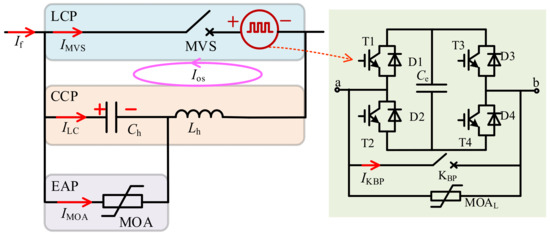
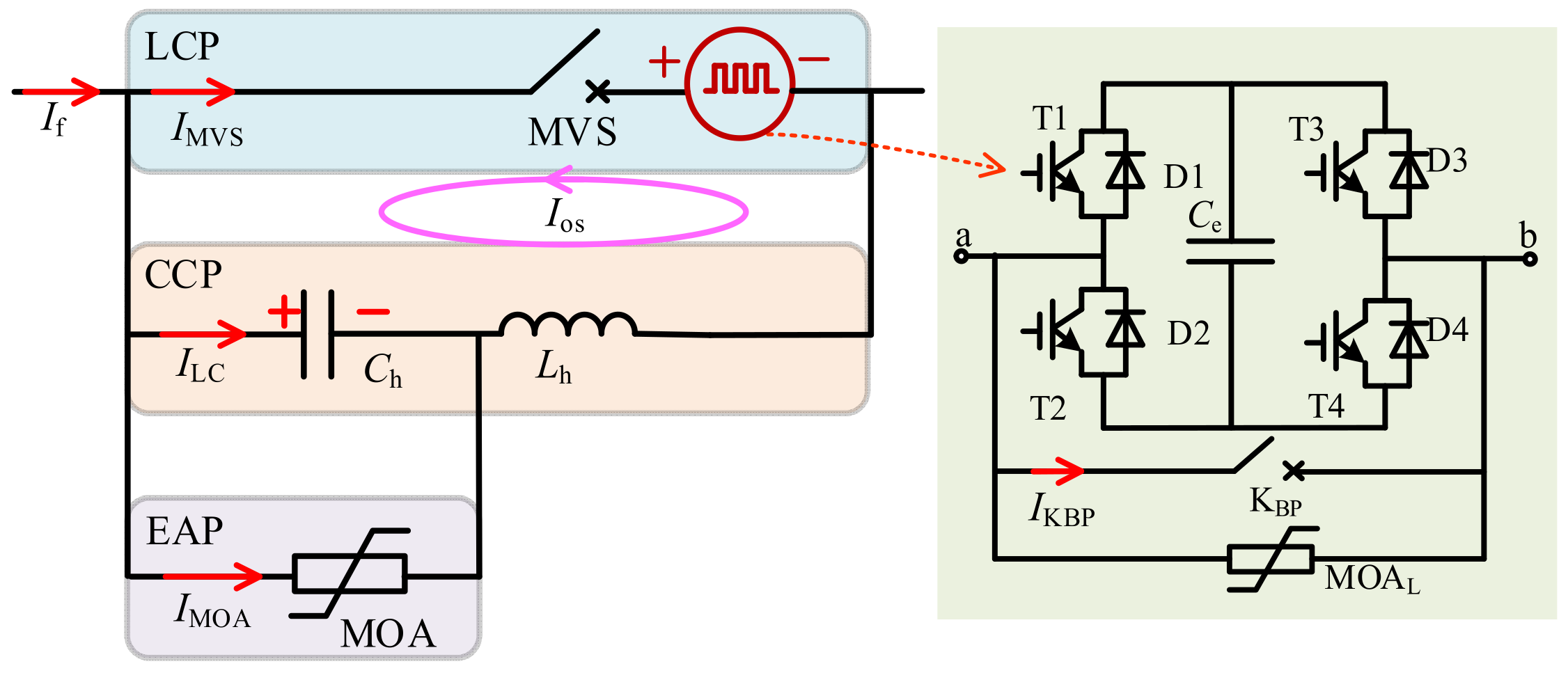
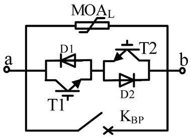
To solve the above problems, a novel resonant DCB with capacitor self-charging by controllable injection energy is proposed, as shown in Figure 7. The proposed RDCB integrates a bypass path switch (KBP), a full bridge equipped with a capacitor (Ce), and a low-voltage metal oxide arrester (MOAL). The topology eliminates auxiliary charging circuits by utilizing the fault current (If) itself as the exclusive charging source. During steady-state operation, If is diverted through the low-impedance KBP path, minimizing conduction losses while maintaining MVS continuity.
Figure 7.
Topology of the proposed RDCB.
The commutation mechanism is governed by an active energy injection strategy. Upon fault inception, KBP and T2/T3 are turned off, forcing If to flow through D1/D4 to charging Ce. The MOAL actively clamps to prevent dielectric breakdown during this transient. Once the charging is completed, T1/T4 and T2/T3 in the full-bridge are alternately turned on to synthesize a square-wave voltage. By controlling Ios and UCES to have the same direction, CES continuously injects energy into the LC components, exciting a gradually increasing Ios until IMVS is forced to zero, ensuring arc extinction. Once the IMVS is forced to zero, the charging path from CES to the LC components is cut off, resulting in the energy injection terminating naturally at the moment of arc extinction.
Since the successful commutation of RDCB depends on the balance between Winj and Wcom, the proposed RDCB features an adaptive energy regulation characteristic. The upper bound of Winj is dictated by the stored energy in the CES (WCES). By dynamically adjusting the Ce charging duration, WCES is precisely modulated, allowing Winj to be controlled for different faults without oversizing the capacitor bank.
3.2. Energy Injection Principle
Assuming a constant current and a linearly varying voltage during the charging process, WCES can be simplified as (4) based on its working principle.
where Ue is the voltage across Ce, and Δt is the charging duration of Ce.
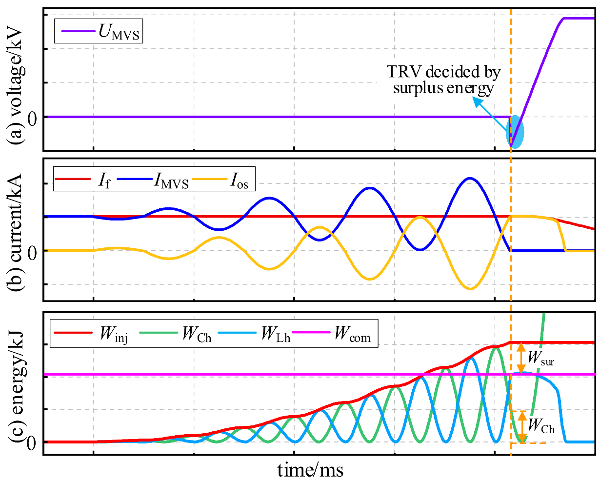
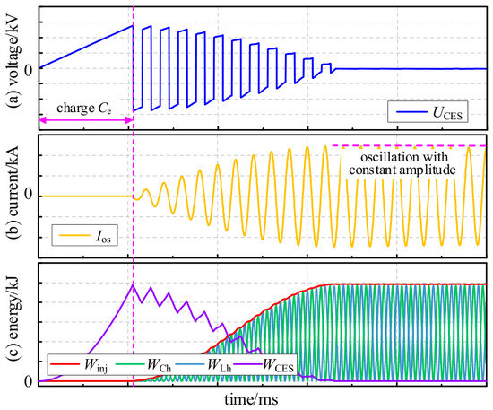
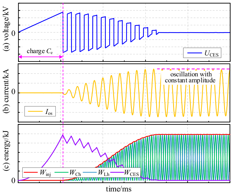
The output square-wave voltage of CES (UCES) is limited by the finite WCES. A typical process of the proposed RDCB is shown in Figure 8. As shown in Figure 8a, UCES gradually decreases, indicating that the gain in each injection cycle continues to drop, leading to a monotonic decline in the incremental oscillation current (ΔIos) and a corresponding reduction in the per-cycle injected energy (ΔWinj).
Figure 8.
Variation in electrical quantities during the interruption process of the proposed RDCB: (a) voltage; (b) current; (c) energy.
Once all WCES are injected into LC components, Ios stops growing and stabilizes at a constant amplitude, as shown in Figure 8b. At this point, no new energy is added to the system, as shown in Figure 8c. The remaining energy simply circulates back and forth between Ch and Lh, sustaining the oscillation without further increasing Ios.
3.3. Adaptive Characteristics of TRV Across MVS
In principle, Wcom is equivalent to the magnetic energy initially stored in Lh, as given by (5).
When WCES is injected into the LC components, the actual Winj is governed by the fault current level and the charging duration of Ce, as shown in (4). To enforce Winj = Wcom, the charging duration must satisfy (6).
No matter how large or small If is, as long as Δt satisfies (6), Winj perfectly matches Wcom, completely eliminating Wsur across the full current range. Consequently, since the TRV across MVS is constrained by Wsur, it can be adaptively suppressed to the lowest possible level regardless of If. Even with a practical safety margin where Winj is slightly larger than Wcom, the adaptive characteristic is preserved. Owing to the self-charging nature of the proposed RDCB, UCES decays progressively as WCES is released. This causes the per-cycle injected energy to diminish gradually. Therefore, the TRV is limited and remains markedly lower than that of RDCBs with a pre-charged capacitor and MOA switching CES.
4. Overvoltage Stress Analysis and Suppression for Internal Components of the Proposed RDCB
4.1. Overvoltage Stress of Ch and Its Suppression
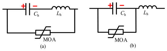
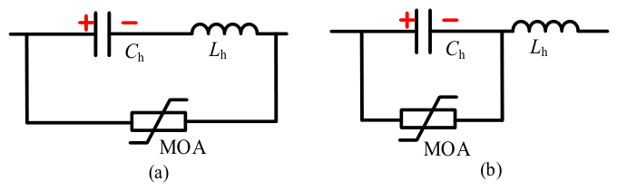
In conventional RDCBs, MOA is typically connected in parallel across the entire CCP branch, which consists of Lh and Ch, as shown in Figure 9a. However, under high fault current conditions in HVDC systems, high-frequency energy injection often results in severe overvoltage across Ch.
Figure 9.
The parallel connection position of MOA and Ch; (a) overall parallel; (b) local parallel.
During the high-frequency commutation stage, the current (itr) exhibits an extremely high rate of ditr/dt. When the total voltage across Lh-Ch reaches the MOA threshold (UMOA_ref), MOA turns on and clamps the external terminal voltage at (UMOA_cl). Nevertheless, according to KVL, the actual voltage stress on Ch is not constant. Instead, it is governed by (7).
At the current zero-crossing instant, the substantial magnetic energy stored in Lh cannot be dissipated through the external MOA branch. Since MOA clamps the terminal voltage of the Lh-Ch assembly, it fails to provide a low-impedance path for the internal reactive power exchange. Consequently, this trapped energy is forced to oscillate within the local loop, resulting in a concealed high-frequency resonance across Ch. The theoretical voltage significantly exceeds the MOA’s clamping level, exhibiting a significant overvoltage. Because this internal overstress is difficult to detect via external monitoring, it remains unmitigated, accelerating dielectric wear-out and ultimately driving the device beyond its safe operating area, resulting in catastrophic avalanche breakdown.
To address the aforementioned limitations, the proposed RDCB adopts a locally paralleled configuration, as shown in Figure 9b. In this topology, the MOA is relocated and directly connected across the terminals of Ch, effectively placing Lh outside the MOA clamping loop.
Consequently, Ch is rigidly bound to the MOA terminal voltage. When the high-frequency oscillating current continuously charges and reaches UMOA_ref, the MOA conducts immediately. By eliminating the effect of Lh, the dynamic voltage stress across is strictly limited to (8).
In this configuration, the magnetic energy stored in Lh is released directly into the external main circuit to facilitate commutation, rather than circulating locally within the submodule. Excess surge energy is safely diverted into the EAP, where it is dissipated as heat via its low-impedance path. This localized paralleling strategy fundamentally disrupts the internal resonant loop, thereby eliminating the overvoltage previously discussed. Consequently, the voltage stress on Ch is strictly maintained below the safety threshold, guaranteeing insulation reliability throughout the service life.
4.2. Overvoltage Stress of CES and Its Suppression
As the key driver of the forced oscillatory commutation in RDCB, CES dictates the ultimate breaking capacity, as this is fundamentally limited by the output voltage stability and the current handling capability of the solid-state switches. To meet these demands, CES typically employs a parallel configuration of multiple IGBTs to achieve the required current rating. However, this parallel topology introduces significant challenges, as it renders the devices susceptible to overvoltage and overcurrent failures during dynamic transients.
Due to unavoidable disparities in IGBT conduction voltage drops and difficulty in achieving perfectly synchronized driving, parallel-connected IGBTs are highly susceptible to severe current imbalances during dynamic switching intervals, potentially triggering localized overcurrent failures in the early-conducting IGBT.
To suppress dynamic current imbalance among parallel branches, the conventional method is to add independent reactors in series with each IGBT path. These reactors exploit the impedance effect of large inductances on di/dt to enforce balanced current distribution, preventing overcurrent. However, these additional series inductors introduce significant penalties. They severely retard the current commutation speed between LCP and both CCP and EAP. Furthermore, they form a series resonant loop with Ch, which degrades the fault interruption capability. Concurrently, the voltage drop across these inductors distorts the square-wave output of CES, thereby reducing the overall commutation efficiency and breaking performance.
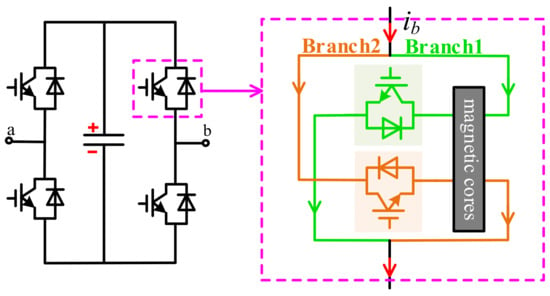
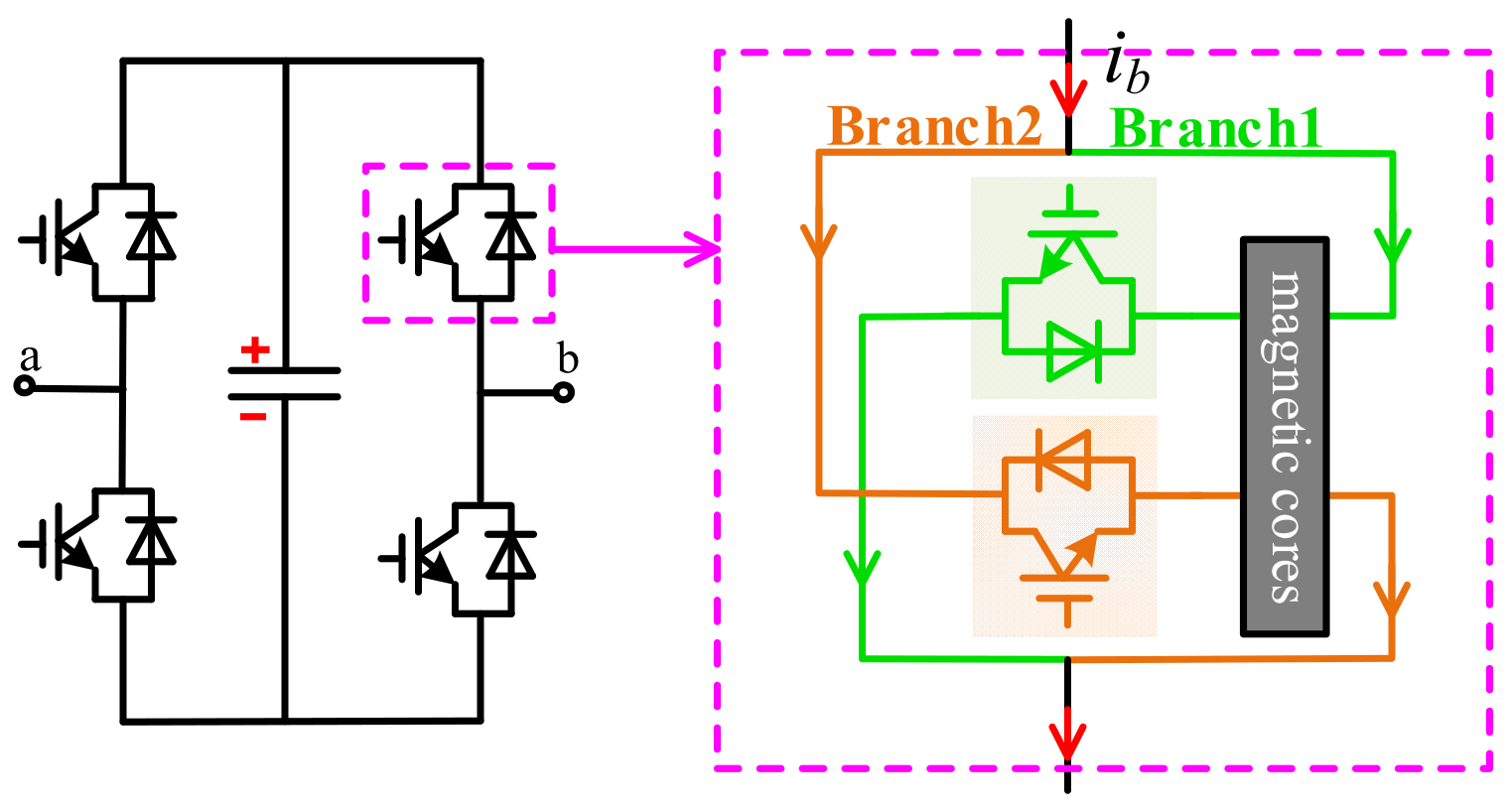
To resolve the aforementioned contradiction, the proposed RDCB introduces the method of embedding the anti-parallel magnetic cores within the IGBT parallel branches of CES. Taking a power electronic module with two parallel IGBTs as an example, as shown in Figure 10, a magnetic core is nested into each branch. Crucially, one branch adopts a forward nesting orientation while the other adopts a reverse nesting orientation.
Figure 10.
Schematic diagram of embedding the anti-parallel magnetic cores within the IGBT parallel branches of CES.
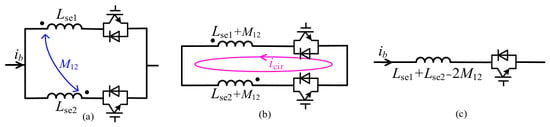
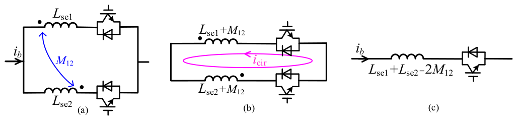
This specific configuration ensures that the currents in the two branches traverse the anti-parallel magnetic core in strictly opposite directions, resulting in the equivalent circuit shown in Figure 11a, where Lse1 and Lse2 are the self-inductances, and M12 is the mutual inductance. When the magnetic cores remain unsaturated, Lse1 = Lse2 ≈ M12.
Figure 11.
Equivalent circuit of magnetic cores: (a) overall equivalent circuit; (b) internal circulating current; (c) external current.
When the IGBTs are not perfectly synchronized during turn-on and turn-off, internal circulating currents are induced within the parallel branches, as shown in Figure 11b. The introduction of the anti-parallel magnetic cores provides a high equivalent self-inductance and mutual inductance for each independent IGBT branch. Acting as independent reactors, these cores present a high impedance that suppresses current imbalances and enforces balanced current distribution during turn-on and turn-off.
For the external current, the two parallel IGBT branches can be reduced to a single equivalent branch, as shown in Figure 11c. With the introduction of the anti-parallel magnetic cores, due to the mutual inductance, the equivalent inductance of this branch is Lse1 + Lse2 − 2M12 ≈ 0. This presents an extremely low inductance to the external circuit, having a negligible impact on the current commutation speed between the LCP and both the CCP and EAP.
The implementation of the anti-parallel magnetic cores design effectively prevents the overvoltage generated by the independent reactors from being superimposed on UCES during IGBT turn-off. Consequently, a stable, distortion-free square-wave voltage can be output by CES without requiring extra stray inductance. This approach not only eliminates the risk of turn-off overvoltage in IGBTs but also ensures rapid current commutation between the LCP and both the CCP and EAP, thereby guaranteeing the reliable interruption of RDCB.
5. Simulation Verification
5.1. System Model
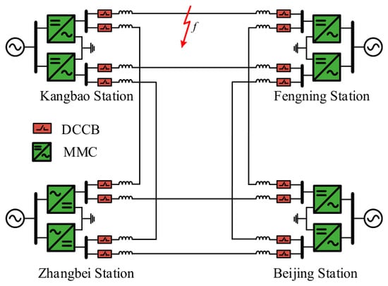
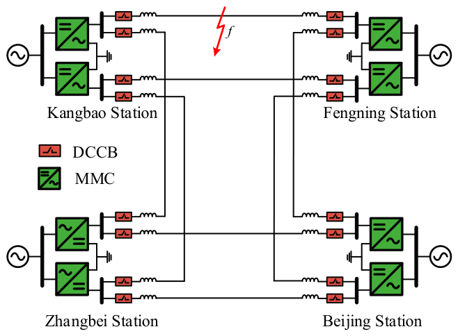
To verify the effectiveness of the proposed RDCB, simulations were conducted on the Zhangbei four-terminal project using PSCAD. The system model is shown in Figure 12, and the parameters are listed in Table 3. To ensure the resonant waveforms remain undistorted, a simulation time step of 1μs and the Intel(R) Visual Fortran Compiler were selected for precise analysis. The MVS is modeled with an opening time of 2 ms and a final contact gap of 26 mm, featuring a time-varying separation speed and a kV/μs-level dynamic dielectric recovery strength [26].
Figure 12.
Schematic diagram of the Zhangbei four-terminal project.
Table 3.
Simulation system parameters.
5.2. Typical Fault Interruption Analysis
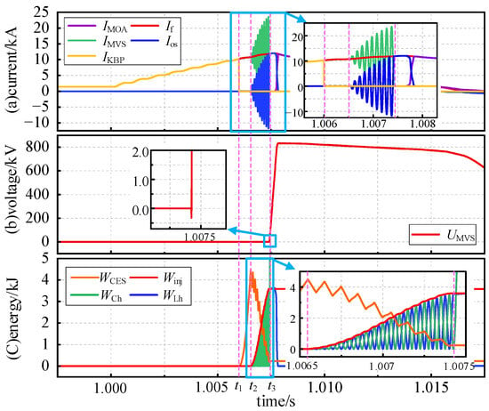
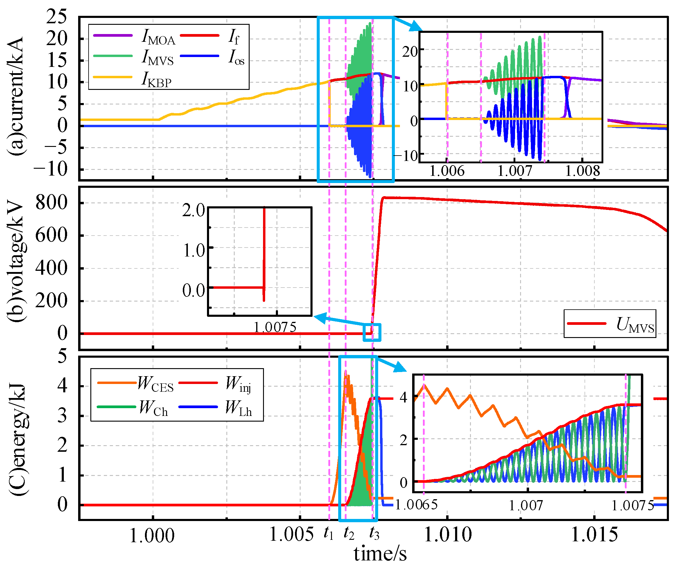
The typical fault interruption waveforms under a fault current of 10 kA are shown in Figure 13.
Figure 13.
Typical waveforms of the fault interruption process.
As shown in Figure 13a, upon fault detection, CES is activated at t1. Meanwhile, KBP and T2/T3 are turned off, and If is commutated to the full-bridge circuit to charge the Ce within the CES. At t2, the charging of Ce is completed. Subsequently, T1/T4 and T2/T3 are conducted alternately, whereby energy is continuously injected into LC components from CES, leading to a gradual increase in the amplitude of Ios. At t3, Ios reaches If, and If is commutated to CCP, thereby charging Ch. Once UCh reaches the reference voltage of the MOA, If is then commutated to the EAP and gradually attenuated to zero through the energy dissipation of MOA.
As shown in Figure 13c, WCES increases gradually during the charging phase of Ce. After charging is completed, energy is periodically transferred from the CES to LC components, causing a continuous decrease in WCES. The energy injection is halted as soon as Ios reaches If. Since Ios is near its peak value at this instant, Winj is primarily concentrated in the Lh, leaving minimal energy in Ch. Consequently, Wsur is negligible, and TRV is suppressed to an extremely low level of 0.3 kV, as shown in Figure 13b, ensuring reliable arc extinction of the MVS.
5.3. Adaptability Analysis of TRV Across MVS for Different Fault Currents
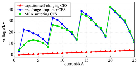
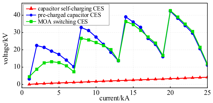
The TRV values generated by the proposed RDCB under different fault currents are shown in Figure 14.
Figure 14.
TRV under different interruption currents.
As shown in Figure 14, compared with RDCB employing pre-charged capacitor CES and MOA switching CES, the proposed RDCB reduces the TRV by a maximum of 96% and a minimum of 64%, significantly reducing TRV during interruption. Particularly under low-current conditions, TRV is nearly zero, enabling overvoltage-free interruption. Regarding the dynamic trend, while TRV of the pre-charged capacitor type and the MOA switching type exhibits periodic variations with increasing current, that of the capacitor self-charging type is stably kept at a low level and shows a slowly rising trend with If increases.
The underlying physical mechanism for these distinct trends is rooted in the energy-matching characteristics of each topology.
For the pre-charged capacitor CES and MOA Switching CES, Winj per oscillation cycle is essentially uncontrollable. Within a specific current range, current interruption successfully occurs inside the same commutation cycle because Wcom remains smaller than or equal to Winj. In this cycle, a smaller If requires less Wcom, leaving a larger Wsur. Consequently, a higher Wsur results in a higher TRV. When If scales up such that the required Wcom exceeds Winj of the current cycle, interruption fails in this cycle, forcing the wait for the next cycle. Since the cumulative injected energy gradually escalates with the number of cycles, a higher If eventually triggers interruption in a later cycle with a much higher total energy injection, thereby leading to an overall increasing TRV trend across different cycle thresholds.
For the capacitor self-charging CES, the energy injection is adaptively regulated. To guarantee reliable current zero-crossing, a pre-designed engineering energy margin is inherently incorporated. As If increases, both the self-charging voltage UCES and Winj per cycle scale up accordingly. Under higher current levels, it becomes slightly more challenging to achieve a perfect energy match, leading to a moderately larger surplus Wsur and TRV. Therefore, the reported TRV for the capacitor self-charging CES exhibits a stable, monotonic growth trend with the increase in If, without the severe step-like fluctuations observed in existing CES.
5.4. Comparative Analysis of Ch Overvoltage Suppression
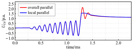
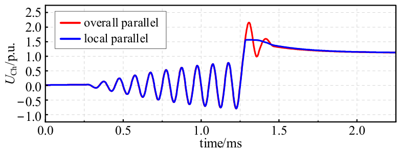
The comparison of the UCh in the proposed RDCB under the full-parallel and partial-parallel MOA configurations is shown in Figure 15.
Figure 15.
Comparison of UCh between full-parallel and partial-parallel structures.
As shown in Figure 15, in the overall parallel structure, the terminals of both Lh and Ch are clamped by MOA. This forces the magnetic energy stored in Lh to recirculate through Ch, triggering a severe overvoltage across Ch. Consequently, UCh escalates to a peak of 2.2 p.u. under high-frequency oscillation, posing a critical threat to the insulation integrity of Ch. In contrast, the proposed local parallel structure shows superior overvoltage suppression performance. Benefiting from the structural advantage of connecting the MOA directly across Ch, the effect of Lh is effectively eliminated. Consequently, the peak voltage is strictly clamped at approximately 1.5 p.u. This represents a significant voltage reduction of about 32%, effectively lowering the voltage requirements for Ch and substantially enhancing operational reliability.
5.5. Comparative Analysis of CES Overvoltage Suppression
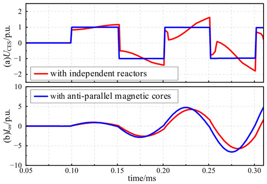
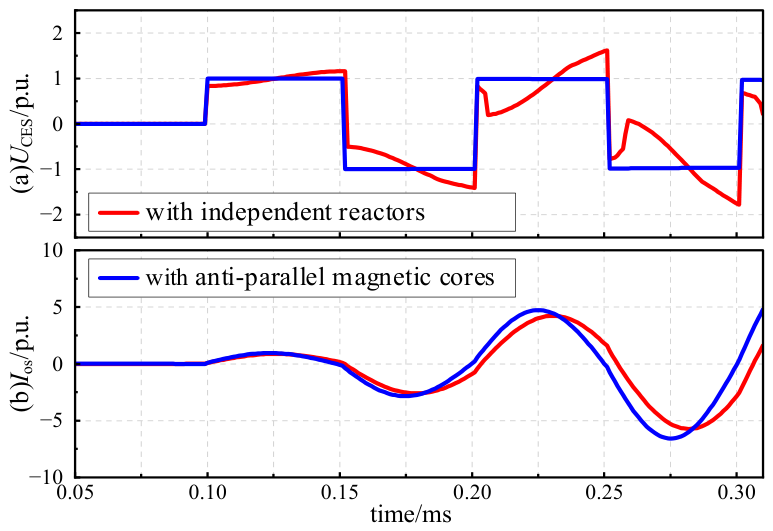
The comparisons of UCES and Ios in the proposed RDCB with independent reactors and the anti-parallel magnetic cores are shown in Figure 16.
Figure 16.
Comparison between RDCB with independent reactors and the anti-parallel magnetic cores; (a) UCES; (b) Ios.
As shown in Figure 16a, the incorporation of independent reactors introduces additional inductance directly into the output voltage loop. Due to the superposition of voltages across these inductors, the actual UCES deviates from the ideal square-wave voltage, generating severe overvoltage spikes up to 1.5 p.u. This significant waveform distortion substantially suppresses the continuous growth of the resonant current. Conversely, with the integration of magnetic cores, the additional inductance is effectively canceled out from the perspective of the output loop. This allows CES to deliver a stable, high-quality square-wave voltage, providing ideal excitation conditions for the resonance process. As shown in Figure 16b, if independent reactors are adopted, their additional inductance inevitably enters the resonant loop, which not only reduces the resonant current amplitude but also decelerates the current rising rate, severely compromising the ability of the system to interrupt fault currents rapidly. In contrast, the proposed magnetic core method avoids these drawbacks, effectively enhancing both the operational performance and reliability of the RDCB under fault conditions.
6. Comparison of Different CESs
To verify the superior performance of the proposed capacitor self-charging CES, a comprehensive comparison is conducted among the capacitor self-charging CES and existing CES (pre-charged capacitor type and MOA switching type) across the terms of economic cost, TRV, and pre-charging requirements. The detailed comparison results are summarized in Table 4.
Table 4.
Comparison of RDCBs with Different CESs.
It is important to note that the primary objective of this study is to address the arc extinction unreliability caused by excessive TRV in existing RDCBs. Therefore, the comparison in Table 4 focuses on TRV performance and interruption reliability, which are the dominant metrics for the proposed topology.
The component pricing is referenced to the core technical data of the CES provided by Henan Pinggao Electric Power Co., Ltd. For instance, the unit costs of high-voltage capacitors and MOAs are set to 2 RMB/J and 30 RMB/kJ, respectively.
Taking a 100 kV/25 kA RDCB as an example, the economic analysis focuses on the cost disparity arising from differences in main components. From a cost perspective, the existing pre-charged capacitor CES consists of a bridge circuit and a pre-charged capacitor. In a full-bridge circuit, a large-capacity capacitor of 23 kJ (3 kV/5 mF) is required, which costs approximately 46,000 RMB. Given that the maximum voltage rating of the IGBTs (4.5 kV/8 kA) is 4.5 kV, four IGBTs are required for the full-bridge circuit, costing approximately 200,000 RMB. Although the number of arms in a half-bridge circuit is reduced, its output voltage must be twice that of the full-bridge circuit to oscillate to the same current level within the same timeframe. Consequently, the capacitance (6 kV/5 mF) must be four times larger, requiring two IGBTs in series per arm to withstand the capacitor voltage, totaling still four IGBTs. Therefore, from an economic perspective, the full-bridge circuit is the most economical, totaling approximately 246,000 RMB. The existing MOA switching CES comprises an MOA, two trigger IGBTs, and a current transfer switch. When the current flows through MOA, approximately 100 kJ of energy must be absorbed, costing about 3000 RMB. Two series-connected IGBTs are required for each current direction to withstand the clamping voltage of the MOA, resulting in a total of four IGBTs with a cost of approximately 200,000 RMB, while a transfer switch rated at 6 kV costs about 10,000 RMB, resulting in a cumulative cost of 213,000 RMB. In comparison, the proposed capacitor self-charging CES consists of a full-bridge circuit with a capacitor, a current transfer switch, and an MOA. The full-bridge circuit cost is virtually identical to that of the pre-charged capacitor CES. With the additional transfer switch and MOA factored in, the total cost is approximately 259,000 RMB. It is noted that in an actual high-voltage DC (HVDC) grid, the economic cost of DCB is vastly dominated by massive infrastructure components, such as MVS, resonant capacitors, and MOA. Taking the Zhangbei ±500 kV project as a reference, the total cost of 500 kV/25 kA/3 ms DCB can reach up to 100 million RMB, whereas the cost of CES accounts for less than 1% of the total. Therefore, the minor component increment introduced by our proposed CES has a negligible economic impact on the system-level effective cost.
Regarding TRV characteristics, as analyzed in Section 3.3, RDCB employing pre-charged capacitors and MOA switching CESs exhibit relatively high TRVs. The former fluctuates repeatedly within a range of 3 kV to 42 kV, whereas the latter fluctuates between 4 kV and 42 kV, both of which pose a high risk of arc re-strikes. In contrast, with the proposed capacitor self-charging CES, TRV is well maintained below 4.5 kV, effectively preventing arc re-strikes.
Regarding the reliability and maintenance, RDCB employing pre-charged capacitor CES exhibits a relatively low long-term reliability due to the persistent risk of MVS re-strikes under unmitigated TRV. Concurrently, their reliance on auxiliary charging infrastructures necessitates regular pre-charging verification checks, increasing operational overhead. For the MOA switching CES, it still suffers from low comprehensive reliability, due to the similar re-strike risks and the inevitable degradation of MOAs subjected to repetitive energy-absorption stresses over time. In contrast, the proposed self-charging RDCB guarantees a small TRV across all conditions by self-adaptively matching the injection energy to the commutation requirements, ensuring reliable arc extinction. Moreover, since no auxiliary pre-charging circuit is required, this topology requires almost no pre-charging checks.
Regarding the pre-charging requirement, the pre-charged capacitor CES requires pre-charging of the capacitor based on the maximum interruption current. In contrast, MOA switching CES uses the nonlinear voltage-current (V-I) characteristics of the MOA for passive clamping, while the proposed capacitor self-charging CES relies on the fault current for active charging. Consequently, both of the latter types do not require pre-charging operations.
7. Conclusions and Future Work
A novel RDCB with capacitor self-charging by controllable injection energy is proposed in this paper, aiming to resolve the conflict between reliable fault interruption and internal overvoltage stress in flexible DC grids. By using the fault current for charging, the proposed RDCB precisely matches Winj with Wcom, thereby suppressing Wsur and limiting TRV. To mitigate component insulation, relocating MOA directly across the capacitor severs the internal local oscillation path, while the anti-parallel magnetic cores enforce dynamic current sharing among parallel IGBTs without introducing external loop inductance. Simulation results confirm that the proposed RDCB ensures current zero-crossing and reduces TRV below 4.5 kV. The proposed self-charging RDCB offers a compact, reliable solution for multi-terminal HVDC grids by eliminating pre-charging peripherals and suppressing TRV across the full current range. Furthermore, the efficacy of the proposed overvoltage suppression methods is verified, thereby guaranteeing reliable interruption across the full current range. Finally, while the current offline fixed charging timing strategy offers zero-latency benefit, it is sensitive to fluctuations under complex grid conditions. Future research will focus on this limitation by implementing a real-time closed-loop correction framework with high-speed sampling and control hardware.
Author Contributions
Conceptualization, W.W. and Y.Z.; methodology, X.H. and B.L.; software, Y.Z.; validation, Y.Z.; formal analysis, Y.Z. and X.H.; investigation, Y.Z., X.H., W.W. and Z.Z.; resources, X.H.; data curation, Y.Z., B.L. and W.W.; writing—original draft preparation, Y.Z., X.H. and W.W.; writing—review and editing, Y.Z., X.H., W.W., B.L. and Z.Z.; visualization, Y.Z., X.H.; supervision, Y.Z., X.H. and W.W.; project administration, X.H. and W.W.; funding acquisition, X.H. All authors have read and agreed to the published version of the manuscript.
Funding
This work is financially supported by the Smart-Grid National Science and Technology Major Project (2026ZD0810200).
Data Availability Statement
All data generated or analyzed during this study are included in this published article.
Conflicts of Interest
Author Xingning Han was employed by State Grid Jiangsu Electric Power Co., Ltd. Author Zhicheng Zhang was employed by Shandong Taikai DC Technology Co., Ltd. The remaining authors declare that the research was conducted in the absence of any commercial or financial relationships that could be construed as a potential conflict of interest.
Abbreviations
The following abbreviations are used in this manuscript:
| DCCBs | DC circuit breakers |
| RDCB | Resonant DC circuit breaker |
| CES | Current excitation source |
| TRV | Transient recovery voltage |
| MOA | Metal oxide arrestor |
| LCP | Load current path |
| CCP | Current commutation path |
| EAP | Energy absorption path |
| MVS | Mechanical vacuum switch |
| Ch | Resonant capacitor |
| Cg | Equivalent gap capacitance of MVS |
| Lh | Resonant inductor |
| If | Fault current |
| IMVS | The current through LCP |
| Ios | Resonant current |
| UCh | Voltage across Ch |
| UCES | Output voltage of the CES |
| UMOA_ref | MOA threshold |
| UMOA_cl | Clamping voltage of MOA |
| Winj | Energy injected into LC components |
| Wcom | Commutation requirement |
| Wsur | Surplus energy |
| WCES | Energy stored in the CES |
| ΔIos | Incremental oscillation current |
| ΔWinj | Incremental injected energy |
| Lse1, Lse2 | Self-inductances of anti-parallel magnetic cores |
| M12 | Mutual inductance anti-parallel magnetic cores |
References
- Adam, G.P.; Ahmed, K.H.; Finney, S.J.; Bell, K.; Williams, B.W. New Breed of Network Fault-Tolerant Voltage-Source-Converter HVDC Transmission System. IEEE Trans. Power Syst. 2013, 28, 335–346. [Google Scholar]
- Sneath, J.; Rajapakse, A.D. Fault Detection and Interruption in an Earthed HVDC Grid Using ROCOV and Hybrid DC Breakers. IEEE Trans. Power Deliv. 2016, 31, 973–981. [Google Scholar] [CrossRef] [Scilit]
- Tang, L.; Ooi, B.-T. Locating and Isolating DC Faults in Multi-Terminal DC Systems. IEEE Trans. Power Deliv. 2007, 22, 1877–1884. [Google Scholar] [CrossRef] [Scilit]
- Ren, C.L.; Hu, Y.G.; Lu, X.; Chen, Y.; Xia, K.P.; Li, H.L. Advanced Non-Unit Protection Strategy for MMC-HVDC Grids Leveraging Two-Dimensional High-Frequency Characteristics via HHT and SVM. Energies 2025, 18, 3096. [Google Scholar] [CrossRef] [Scilit]
- Heidary, A.; Niasar, M.G.; Marvasti, F.D.; Popov, M. Superconducting Magnetic Energy Storage-Based DC Circuit Breaker for HVDC Applications. IEEE Trans. Power Electron. 2024, 39, 13890–13899. [Google Scholar] [CrossRef] [Scilit]
- Liu, Z.; Mirhosseini, S.S.; Liu, L.; Popov, M.; Ma, K.; Hu, W. A Contribution to the Development of High-Voltage DC Circuit Breaker Technologies: A Review of New Considerations. IEEE Ind. Electron. Mag. 2022, 16, 42–59. [Google Scholar]
- Mohammadi, F.; Rouzbehi, K.; Hajian, M.; Niayesh, K.; Gharehpetian, G.B.; Saad, H.; Ali, M.H.; Sood, V.K. HVDC Circuit Breakers: A Comprehensive Review. IEEE Trans. Power Electron. 2021, 36, 13726–13739. [Google Scholar] [CrossRef] [Scilit]
- Davidson, C.; Grieshaber, W.; Modéer, T.; Smith, D.; Yang, B.; Yu, Z.; Zhang, R. DC Circuit Breakers for High-Voltage dc Grids: Present and Future. IEEE Power Energy Mag. 2024, 22, 87–99. [Google Scholar] [CrossRef] [Scilit]
- Häfner, J. Proactive hybrid HVDC breakers—A key innovation for reliable HVDC grids. In Proceedings of the CIGRE Bologna Symposium, Bologna, Italy, 13–15 June 2011. [Google Scholar]
- Zhang, B.; Zhang, X.; He, T.; Qi, L. Capacitor-Split Assist Switch Driven Resonant DC Circuit Breaker with Reduced Mechanical Switch Interruption Stress. In Proceedings of the 2025 IEEE International Conference on Power Electronics, Smart Grid, and Renewable Energy (PESGRE), Dharwad, India, 18–21 December 2025. [Google Scholar]
- Ängquist, L.; Norrga, S.; Modéer, T. A new dc breaker with reduced need for semiconductors. In 2016 18th European Conference on Power Electronics and Applications (EPE’16 ECCE Europe), Karlsruhe, Germany, 5–9 September 2016; IEEE: Piscataway, NJ, USA, 2016; pp. 1–10. [Google Scholar]
- Wen, W.; Wang, Y.; Li, B.; Huang, Y.; Li, R.; Wang, Q. Transient Current Interruption Characteristics of a Novel Mechanical DC Circuit Breaker. IEEE Trans. Power Electron. 2018, 33, 9424–9431. [Google Scholar]
- Augustin, T.; Becerra, M.; Nee, H.-P. Enhanced Active Resonant DC Circuit Breakers Based on Discharge Closing Switches. IEEE Trans. Power Deliv. 2021, 36, 1735–1743. [Google Scholar] [CrossRef] [Scilit]
- Wang, Y.; Wang, S.; Ugalde-Loo, C.E.; Ming, W.; Li, W. Low-loss bidirectional solid-state circuit breakers with reliable breaking capability for protecting DC microgrids. IEEE Trans. Power Electron. 2023, 38, 15432–15445. [Google Scholar] [CrossRef] [Scilit]
- Huang, X.; Wen, W.; Zhang, Z.; Sun, Q.; Fan, J.; Zhang, C. Low-Cost Multiport DC Transfer Switch for HVDC System Based on Line Commutated Converter. IEEE Trans. Power Electron. 2026, 41, 4117–4127. [Google Scholar]
- Wang, X.; Zhao, Z.; Yuan, L. Current sharing of IGBT modules in parallel with thermal imbalance. In Proceedings of the IEEE Energy Conversion Congress and Exposition, Atlanta, GA, USA, 12–16 September 2010; IEEE: Piscataway, NJ, USA, 2010; pp. 2101–2108. [Google Scholar]
- Belda, N.A.; Plet, C.A.; Smeets, R.P.P. Analysis of Faults in Multiterminal HVDC Grid for Definition of Test Requirements of HVDC Circuit Breakers. IEEE Trans. Power Deliv. 2018, 33, 403–411. [Google Scholar] [CrossRef] [Scilit]
- Pithanisetty, P.; Dsa, D.; Ghadrdan, M.; Banavath, S.N.; Carvalho, G. A Reconfigurable Series/Parallel IGBT-Based DC Solid-State Circuit Breaker. In Proceedings of the 2025 IEEE International Conference on Power Electronics, Smart Grid, and Renewable Energy (PESGRE), Dharwad, India, 18–21 December 2025. [Google Scholar]
- Li, H.; Munk-Nielsen, S.; Wang, X.; Maheshwari, R.; Bęczkowski, S.; Uhrenfeldt, C. Influences of Device and Circuit Mismatches on Paralleling Silicon Carbide MOSFETs. IEEE Trans. Power Electron. 2016, 31, 621–634. [Google Scholar] [CrossRef] [Scilit]
- Lobsiger, Y.; Bortis, D.; Kolar, J.W. Decentralized active gate control for current balancing of parallel connected IGBT modules. In Proceedings of the 2011 14th European Conference on Power Electronics and Applications (EPE ’11 ECCE Europe), Birmingham, UK, 30 August–1 September 2011; pp. 1–10. [Google Scholar]
- Liu, S.; Popov, M.; Mirhosseini, S.S.; Nee, S.; Modeer, T.; Ångquist, L.; Belda, N.; Koreman, K.; van der Meijden, M.A.M.M. Modeling, experimental validation, and application of VARC HVDC circuit breakers. IEEE Trans. Power Deliv. 2020, 35, 1515–1526. [Google Scholar] [CrossRef] [Scilit]
- Ängquist, L.; Nee, S.; Modeer, T.; Baudoin, A.; Norrga, S.; Belda, N.A. Design and test of VSC assisted resonant current (VARC) DC circuit breaker. In 15th IET International Conference on AC and DC Power Transmission (ACDC 2019), Coventry, UK, 5–7 February 2019; Institution of Engineering and Technology (IET): London, UK, 2019; pp. 1–8. [Google Scholar]
- Chen, Z.; Wu, Y.; Wu, Y.; Zhang, J.; Niu, C.; Rong, M. A Resonant DC Interruption Scheme Based on External Transverse Magnetic Field. IEEE Trans. Power Electron. 2026, 41, 13814–13823. [Google Scholar] [CrossRef] [Scilit]
- Augustin, T.; Parekh, M.; Magnusson, J.; Becerra, M.; Nee, H.-P. Thomson-Coil Actuator System for Enhanced Active Resonant DC Circuit Breakers. IEEE J. Emerg. Sel. Top. Power Electron. 2022, 10, 800–810. [Google Scholar] [CrossRef] [Scilit]
- Zhang, B.; Zhang, X.; Wu, S.; Zhan, L.; Qi, L. A Novel Dual-LC Resonant DC Circuit Breaker Employing Soft-Switching Technique for Enhanced Performance. IEEE Trans. Ind. Electron. 2024, 71, 9023–9033. [Google Scholar] [CrossRef] [Scilit]
- Wen, W.J.; Huang, Y.; Al-Dweikat, M.; Zhang, Z.; Cheng, T.; Gao, S.; Liu, W. Research on Operating Mechanism for Ultra-Fast 40.5-kV Vacuum Switches. IEEE Trans. Power Deliv. 2015, 30, 2553–2559. [Google Scholar] [CrossRef] [Scilit]

Disclaimer/Publisher’s Note: The statements, opinions and data contained in all publications are solely those of the individual author(s) and contributor(s) and not of MDPI and/or the editor(s). MDPI and/or the editor(s) disclaim responsibility for any injury to people or property resulting from any ideas, methods, instructions or products referred to in the content. |
© 2026 by the authors. Licensee MDPI, Basel, Switzerland. This article is an open access article distributed under the terms and conditions of the Creative Commons Attribution (CC BY) license.