


Abstract
High-efficiency and high-power-density point-of-load (POL) converters are critical for data center power supplies. Although hybrid resonant switched-capacitor (ReSC) converters can substantially reduce the volume of passive components, they often suffer from severe efficiency degradation when the switching frequency mismatches the resonant frequency due to component tolerances. To address this challenge, this paper proposes a parameter-mismatch insensitive cascaded POL converter by integrating a BUCK stage with a cascaded voltage divider (CVD). By introducing an auxiliary resonant branch, a multi-resonant operation is established, enabling the residual inductor energy caused by component variations to be transferred to the output during the dead time with virtually eliminated hard-switching losses. Consequently, precise matching between the switching frequency and the resonant frequency is no longer mandatory. A 12 V-to-1 V/30 A GaN-based prototype was developed to validate the theoretical analysis. Experimental results demonstrate that the proposed converter maintains high efficiency under a ±10% component variation and achieves robust voltage regulation and fast transient response, making it highly suitable for high-current data center applications.
1. Introduction
As the amount of information processed and stored by data centers continues to increase, rack power densities have escalated from traditional 5–10 kW to over 30 kW. Consequently, there are higher requirements for the energy consumption level and volume of key equipment in data centers. Specifically, for board-level power distribution architectures, the single-phase or single-module point-of-load (POL) converters discussed in this study typically cover a unit power range of 20 W to 60 W, operating with a nominal 12 V input and an ultra-low output voltage around 1.0–1.5 V to deliver large continuous currents of 20 A to 50 A per unit [1,2,3]. As an important component of the power supply system in data centers, the point-of-load (POL) converter is located at the terminal position of the power supply system, providing power to FPGA, CPU, memory, and other important electronic load units. It is one of the core components that determine the energy efficiency and performance of data centers [4,5,6]. In the power supply topology, the loss at the POL level is the largest. Even a 1% efficiency improvement in the POL stage yields meaningful system-level gains. In modern multi-megawatt data centers, where thousands of POL converters operate simultaneously in close proximity to processing units, a 1% reduction in power loss directly translates to tens of kilowatts of saved electrical energy. Furthermore, this reduction in dissipated heat minimizes the cascading thermal management and cooling overhead, leading to substantial long-term operational cost savings. Therefore, for high-current data center applications, developing novel POL converters with high efficiency and high power density carries profound engineering value [7].
Currently, the most commonly used POL converter in industry basically adopts the circuit topology of the BUCK converter. However, when the voltage conversion ratio (VCR) and the load current are large, the disadvantages of low efficiency and low power density of the BUCK-type POL converter become very obvious. Since there is no power inductor, the switched-capacitor (SC) converter has become a popular choice for designing high-efficiency and high-power-density DC-DC converters [8,9,10]. However, there are some inherent problems with the SC converter that need to be addressed. When two capacitors with different voltage potentials exchange energy in the SC converter, due to the transient voltage differences and mismatched capacitance values, a relatively high initial peak current occurs, resulting in significant inherent charging and blooming losses [11,12]. To mitigate this critical peak current and achieve complete or partial soft-charging operations, various advanced methodologies have been actively explored. Specifically, several specific control strategies, such as split-phase switching techniques and frequency modulation, have been implemented to suppress the initial shock current [13,14,15]. Concurrently, structural modifications featuring multi-stage modular paths or passive snubber auxiliary networks have been integrated into the converters to absorb or re-route the lossy charge [16,17]. Each of these approaches uniquely addresses specific dimensions of peak current suppression in modern high-density hardware integration.
To solve the above problems, the soft switching of the power switches and the soft charging of the capacitors can be realized by introducing small inductors to form hybrid resonant switched-capacitor (ReSC) converters [18,19]. However, the resonant switched-capacitor converter is sensitive to the switching frequency and requires ensuring that the switching frequency matches the resonant frequency to ensure that the circuit operates in the resonant working mode [20,21]. According to the position of the inductor, the hybrid resonant switched-capacitor converter can be divided into a direct resonant switched-capacitor converter and an indirect resonant switched-capacitor converter [22,23,24]. The direct resonant switched-capacitor converter realizes the soft charging of the flying capacitor by placing the resonant inductor at the output end of the converter. Although the direct resonant switched-capacitor converter can control the VCR by adjusting the duty cycle of the power switches, its control algorithm is overly complex, and the soft-switching implementation requires multiple intermediate working modes, which is unfavorable for practical engineering applications [25]. The indirect resonant switched-capacitor converter realizes the soft charging of the flying capacitor and the soft switching of the power switches by cascading a small inductor in series with the flying capacitor to form an LC resonator. The VCR of the indirect resonant switched-capacitor converter is closely related to the number of power switches, and its output voltage regulation capability is poor. To achieve a larger VCR, a large number of power switches and passive components are required, but its control method is relatively simple. It only needs to set the duty cycle of the power switches to be close to 50% [26,27].
To address this issue, this paper introduces a parallel resonant capacitor to form a secondary resonant branch. During the dead time, the energy stored in the resonant inductor is transferred to the output side without loss; consequently, an exact match between the resonant frequency and the switching frequency is no longer a prerequisite. The remainder of this paper is organized as follows: Section 2 (Materials and Methods) outlines in detail the theoretical framework and design methodology; it establishes the baseline operation of the conventional cascaded converter, derives a quantitative mathematical model of component mismatch limits, uncovers the proposed multi-resonant mechanism with step-by-step circuit state derivations, and presents the precise parameter sizing guidelines for the auxiliary branch. Section 3 (Results) evaluates the comprehensive performance validation, incorporating both PLECS software simulations and empirical data from a 12 V-to-1 V/30 A GaN-based hardware prototype under steady-state, transient, and frequency offset stress conditions. Section 4 (Discussion) deeply analyzes the industrial viability, gate-drive alignment boundaries, and future multi-module parallel current-sharing scalability. Finally, Section 5 (Conclusions) provides the concluding remarks and summarizes the key deliverables of this study.
2. Materials and Methods
2.1. Operation Principle of Cascaded POL Converter
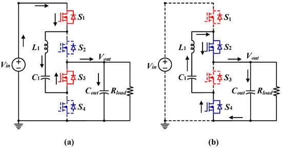
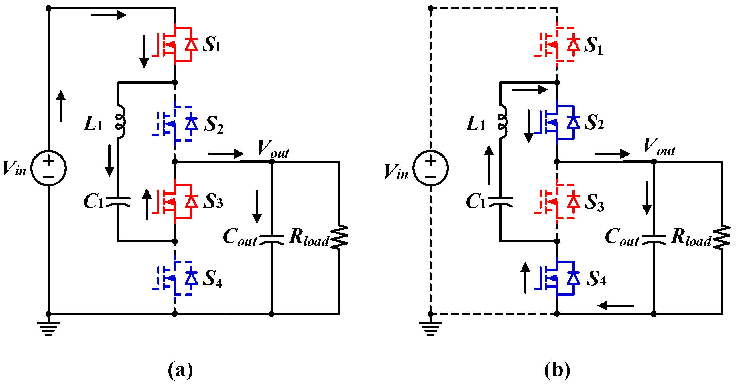
The working principle of the 2:1 indirect resonant switched-capacitor converter is shown in Figure 1. It consists of four power switches and one flying capacitor, achieving a VCR of 2:1.
Figure 1.
2:1 indirect ReSC converter working principle: (a) working mode 1 and (b) working mode 2.
By matching the parameters of an inductor and the flying capacitor and connecting them in series to form an LC resonator, the corresponding circuit topology is a 2:1 indirect ReSC converter. This circuit topology is also commonly referred to as a cascaded voltage divider. Due to the resonance between the inductor and the capacitor, the current flowing through the inductor and the capacitor presents a weakly damped sine wave, and its oscillation period τ is
Here, R represents the relevant resistor of the current flow path. When , the above equation is approximately valid. This assumption, aimed at minimizing losses, is reasonable in practical component design. To achieve soft switching, the switching frequency fs must match the resonant frequency f0 = 1/τ, that is
The working modes of the 2:1 indirect ReSC can be divided into two.
Working mode 1: As shown in Figure 1a, the odd-numbered switch devices (Sn, n = 1, 3) marked in red are turned on, while the even-numbered switch devices (Sn, n = 2, 4) marked in blue are turned off. A direct current voltage is applied to charge the resonant capacitor C1 and the output capacitor Cout.
Working mode 2: As shown in Figure 1b, the odd-numbered switch devices (Sn, n = 1, 3) marked in red are turned off, while the even-numbered switch devices (Sn, n = 2, 4) marked in blue are turned on. The resonant capacitor C1 charges the output capacitor Cout. If the output voltage is Vout, then the maximum voltage borne by all the switch devices is Vout.
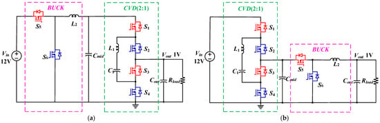
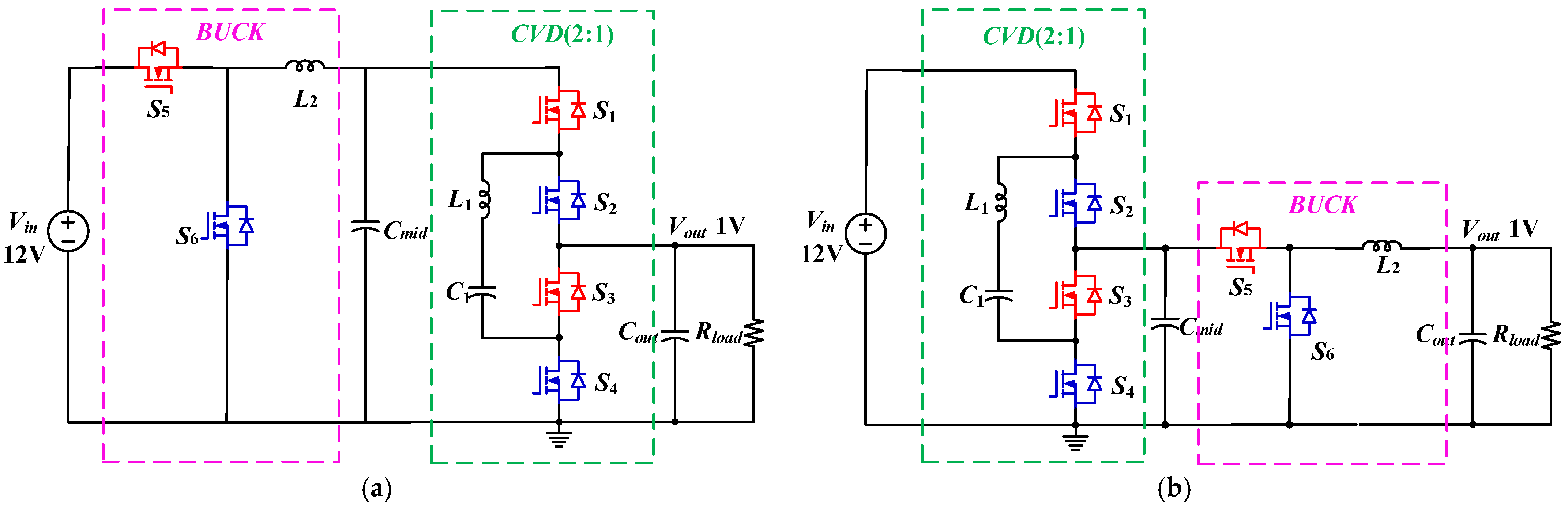
The schematic diagram of the cascaded DC-DC converter based on the 2:1 indirect ReSC converter is shown in Figure 2. By placing the BUCK converter at the front or back end, two new types of cascaded POL converters can be formed.
Figure 2.
The schematic diagram of the new cascaded POL converter (a) BUCK + CVD(2:1) (b) CVD(2:1) + BUCK.
In order to verify the correctness of the proposed novel cascaded POL converter theory, this paper builds the relevant simulation model using the PLECS 5.0.6 simulation software. The relevant parameters of the simulation are shown in Table 1.
Table 1.
Key circuit parameters for PLECS simulation.
As detailed in Table 1, the nominal intermediate voltage (Vmid) across the cascaded voltage divider stage is exactly half of the input voltage, sitting at 6 V due to the 2:1 conversion ratio. Furthermore, the main resonant frequency (fr) of the indirect ReSC converter is determined by the series combination of the resonant inductor L1 and the equivalent resonant capacitor C1. By substituting the selected passive component values, L1 = 100 nH and C1 = 2.82 μF, into Equation (2), the theoretical resonant frequency is calculated to be approximately 300 kHz. This calculation ensures that the switching frequency is properly aligned with the tank’s natural resonance during the simulation.
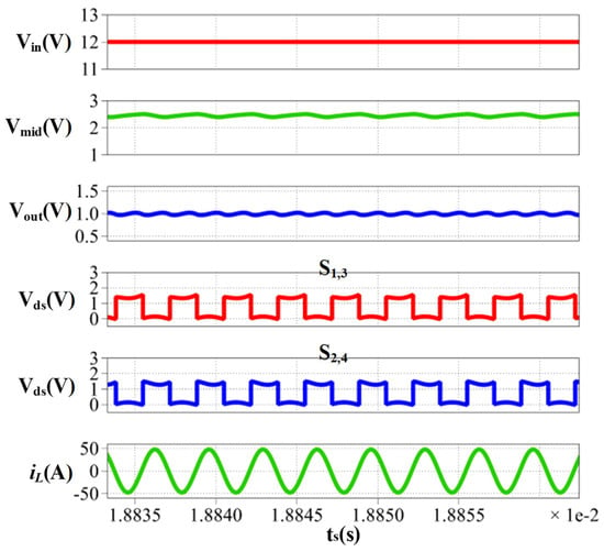
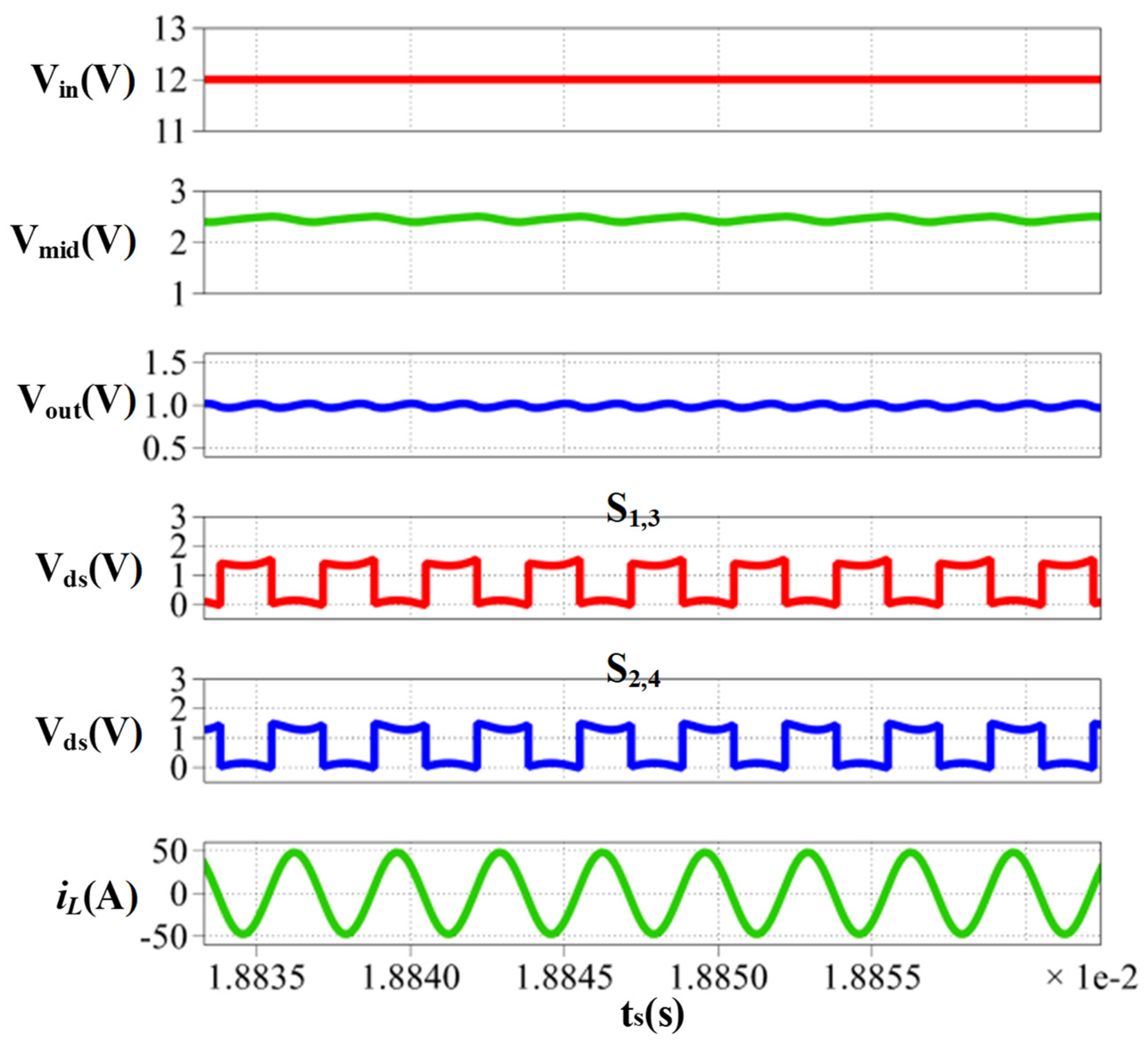
The key simulation waveforms of the BUCK + CVD(2:1) cascaded POL converter are shown in Figure 3. The labels of the power devices in the figure are the same as those in the schematic diagram of the cascaded POL converter in Figure 2. The BUCK + CVD(2:1) type POL converter can achieve a voltage transformation from 12 V to 1 V. The voltage Vds borne by all power devices is equal to the output voltage Vout (1 V), and the current waveform of the resonant inductor in the converter is a sine wave. The simulation results are consistent with the previous theoretical analysis. The relevant parameters of the simulation are shown in Table 1. The input voltage and output voltage are 12 V and 1 V, respectively, and the output current range is 0 to 30 A.
Figure 3.
Key waveforms of the BUCK + CVD(2:1) POL converter.
2.2. Analysis of Parameter Differences in LC Resonator Components
In order to reduce the deviation between the resonant frequency and the switching frequency, Ref. [1] chose a type-I capacitor with a smaller tolerance as the resonant capacitor. Type I capacitors, such as C0G, U2J and NP0, provide stable capacitance values by using low dielectric materials, with very small capacitance deviation. Although Type I capacitors have relatively stable capacitance values, the capacitance deviation is only less than 5%. However, the inductance sensitivity of resonant inductors also has certain deviations, and in practical applications, compared to Type I capacitors, Type II capacitors are more commonly used. Most resonant switched-capacitor converter topologies use Type II ceramic capacitors, such as X7R, X5R and X7S, etc. These capacitors have a very wide tolerance range in terms of temperature, DC bias and component differences, and their capacitance deviation is generally less than 20%.
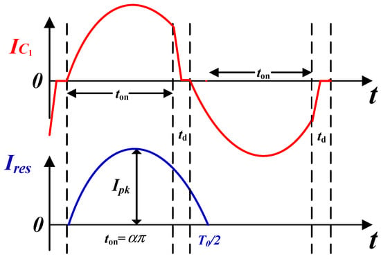
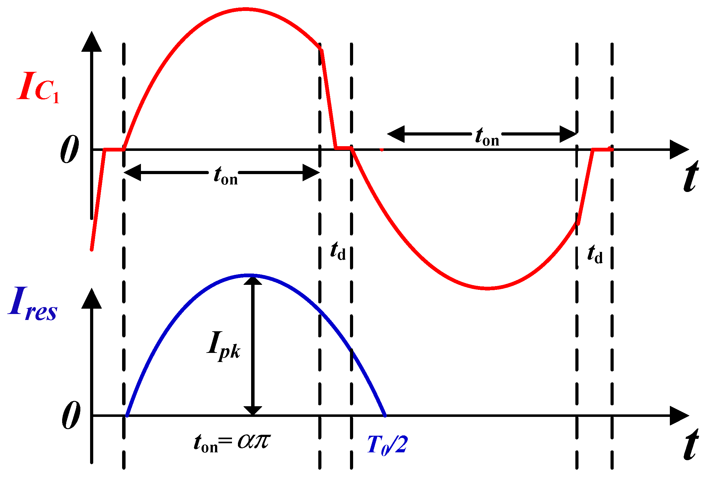
When the switching frequency fs is not consistent with the resonant frequency f0, the indirect ReSC converter needs to add some dead time td to ensure that the resonant inductor current drops to 0 before the next operating mode begins. The influence of the ratio of fs/f0 on the conduction loss can be quantitatively analyzed by modeling the current waveform of the resonant capacitor C1. When the frequencies are not consistent, the comparison diagram of the C1 current and the resonant current is shown in Figure 4.
Figure 4.
Capacitor C1 current and resonant current comparison diagram.
Based on the foundational charge-balance analysis for resonant switched-capacitor converters, within half a cycle, the current IC1 on the resonant capacitor C1 can be described as:
It is critical to note that the behavior of the peak current Ipk is fundamentally asymmetric depending on whether k < 1 or k > 1.
When k < 1 (fs < f0), the switching period is longer than the resonant period. Consequently, the resonant current naturally reaches zero and enters a discontinuous conduction mode characterized by a zero-current plateau. Under this condition, Ipk is independently determined by the resonant tank’s characteristic impedance and the initial voltage difference, remaining largely unaffected by the exact switching instant.
Conversely, when k > 1 (fs > f0), the switching period is shorter than the resonant period. The power switches are forced to turn off before the current naturally reaches zero, abruptly truncating the resonance. This forced continuous or truncated conduction mode alters the charge transfer dynamics, leading to significant non-zero turn-off currents and causing the mathematical behavior of Ipk to diverge asymmetrically compared to the k < 1$ scenario.
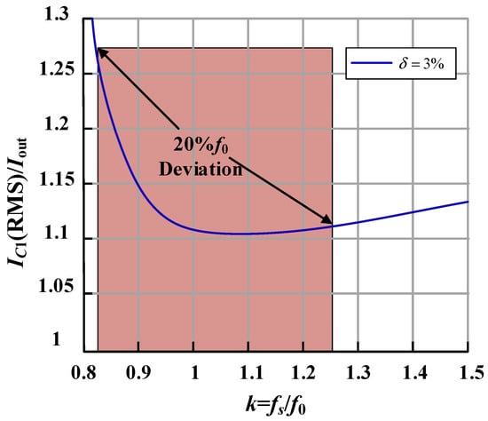
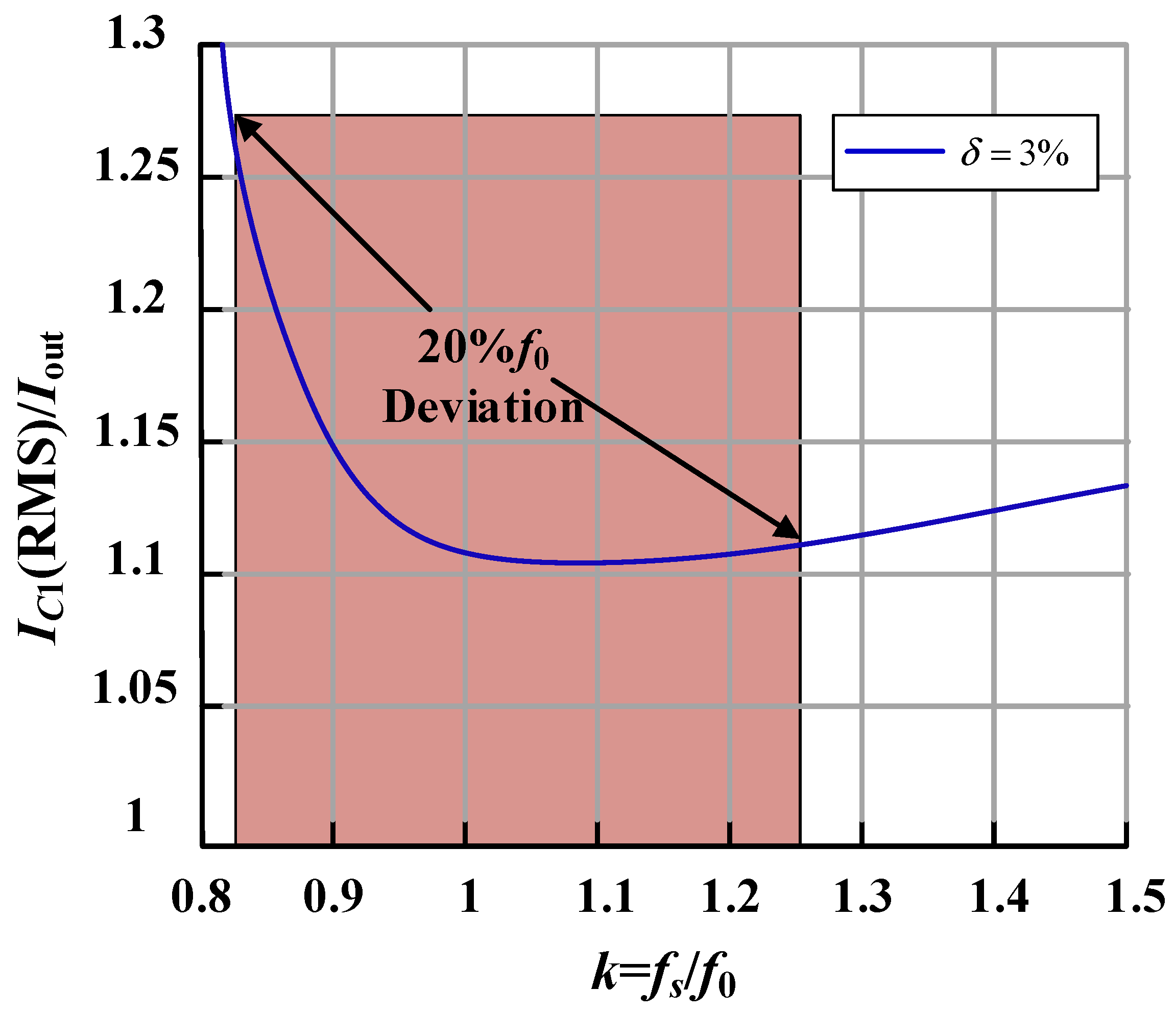
When Ic1(rms) is normalized to Iout, a curve of k = fs/f0 versus the effective value of the resonant capacitor current can be plotted as shown in Figure 5. Considering that the resonant frequency f0 has a 20% deviation, the analysis should be conducted within the range of 0.833 < k < 1.25. As shown in Figure 5, the normalized value of the current across the bypass capacitor C1 fluctuates between 1.1 and 1.27. Since the loss on the capacitor can be estimated using the equivalent series resistance (ESR) of the capacitor based on IRMS2*ESR, when the effective value flowing through the capacitor increases, it will significantly affect the efficiency of the indirect ReSC converter.
Figure 5.
The effective value of the current of capacitor C1 varies with the value of K.
2.3. Mechanism of the Multi-Resonant 2:1 Indirect ReSC Converter
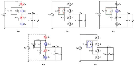
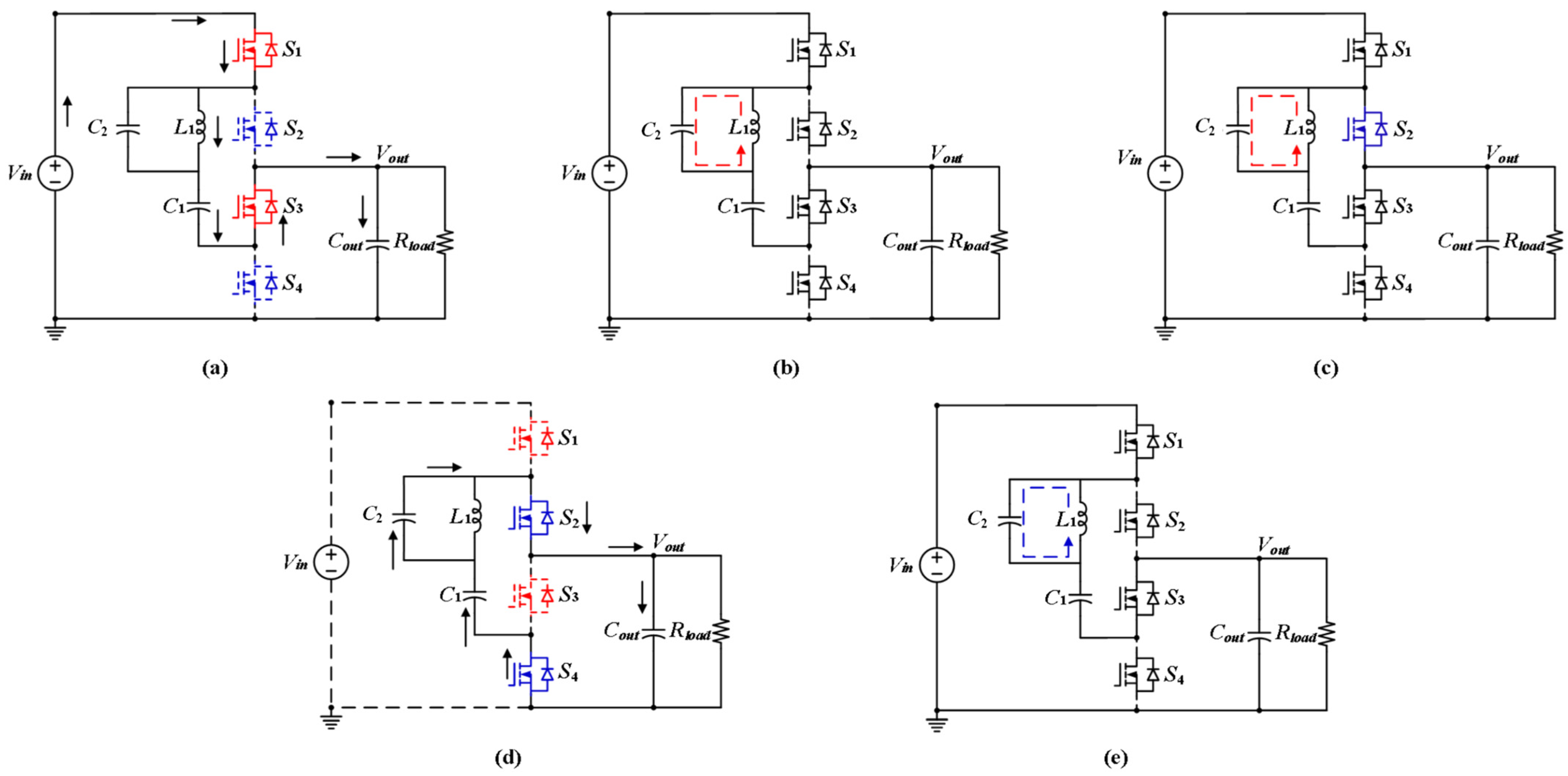
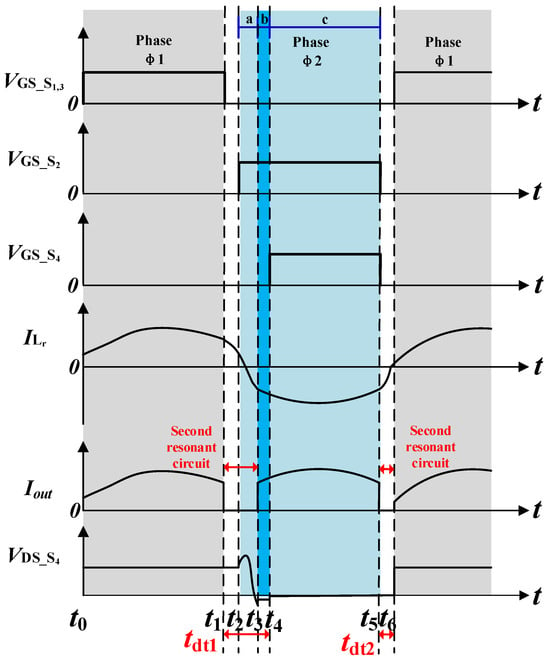
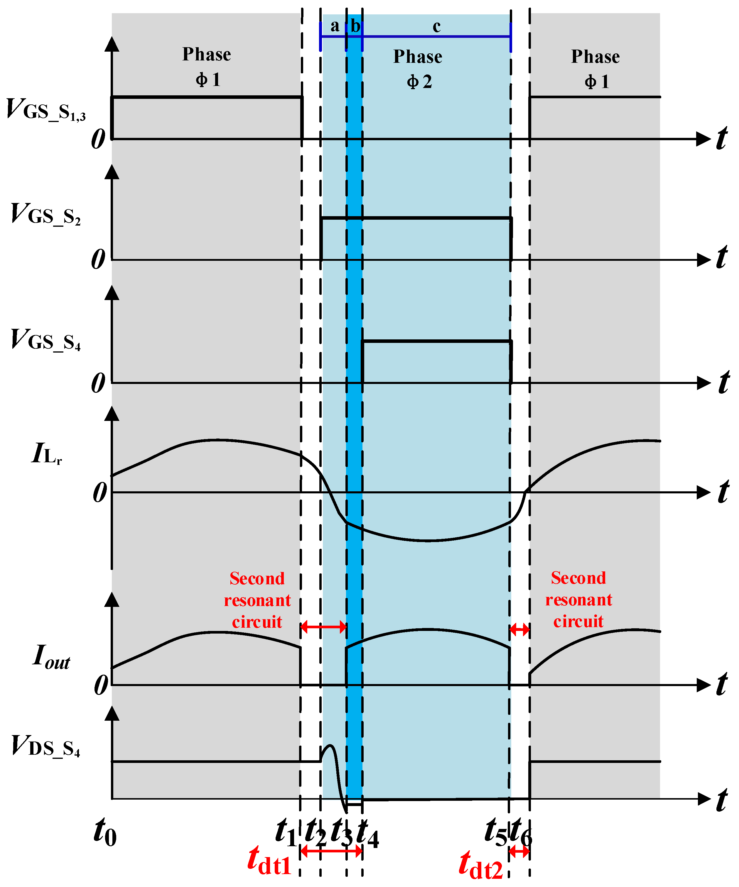
The working principle and control logic waveform diagrams of the multi-resonant 2:1 indirect ReSC converter are shown in Figure 6 and Figure 7, respectively. They respectively illustrate the circuit topology and corresponding voltage and current waveforms under different working modes. The related control logic can be divided into two working modes (i.e., two phases) by the dead time.
Figure 6.
Block diagram of the multi-resonant CVD(2:1) converter working principle (a) mode1 (b) mode 2 (c) mode 3 (d) mode 4 (e) mode 5.
Figure 7.
Control logic waveform diagram of multi-resonant CVD(2:1) converter.
In the first phase (phase 1, t0 < t < t1), it is similar to the traditional indirect ReSC converter. Power devices S1 and S3 are turned on, and the input voltage Vin charges the resonator L1C1 and the output capacitor Cout.
After the working mode 1, there is the first dead time td-t1 (t1 < t < t2), during which all power devices are turned off. However, since fs > f0, there is residual current in the inductor L1 at the moment when td-t1 begins. And due to the introduction of the second resonant capacitor C2, the residual current in the inductor starts flowing to the capacitor C2, and the second resonator L1-C2 begins to resonate.
After the first dead time, the working mode 2 (phase 2) begins, and power device S2 is turned on at t = t2. At this moment, no new current conduction path is generated, and the drain voltage of power device S2 is equal to the output voltage Vout. The second resonator continues to resonate (as shown in phase 2a in Figure 7, t2 < t < t3), and at some point, the drain-source voltage Vds4 of power device S4 will become negative.
At t = t3, the voltage value of Vds4 becomes low enough to trigger the reverse conduction process in power device S4, which is achieved through the conducting channel in the enhancement-mode GaN power device. During phase 2b (t3 < t < t4), the energy stored in the second resonator L1-C2 begins to be released to the output terminal. After the additional dead time (t2 < t < t4) ends, power device S4 is turned on, thus finally achieving complete conduction during phase 2c (t4 < t < t5), ensuring the transmission of energy to the output terminal with lower loss.
The time interval [t2, t4] is called the additional dead time. At the end of working mode 2 (phase 2), there will be a second dead time (t5 < t < t6), during which the second resonator resonates again, thus retaining the energy for the next stage. After that, the cycle will restart from phase 1.
In the control waveform shown in Figure 7, the resonant frequency of the main resonator is lower than the switching frequency. The remaining energy in the resonant inductor L1 will be stored in the second resonator until the power device S4 conducts in reverse, causing the main resonator to recover. At this point, the control signal is fully conducting.
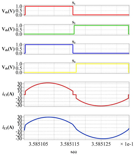
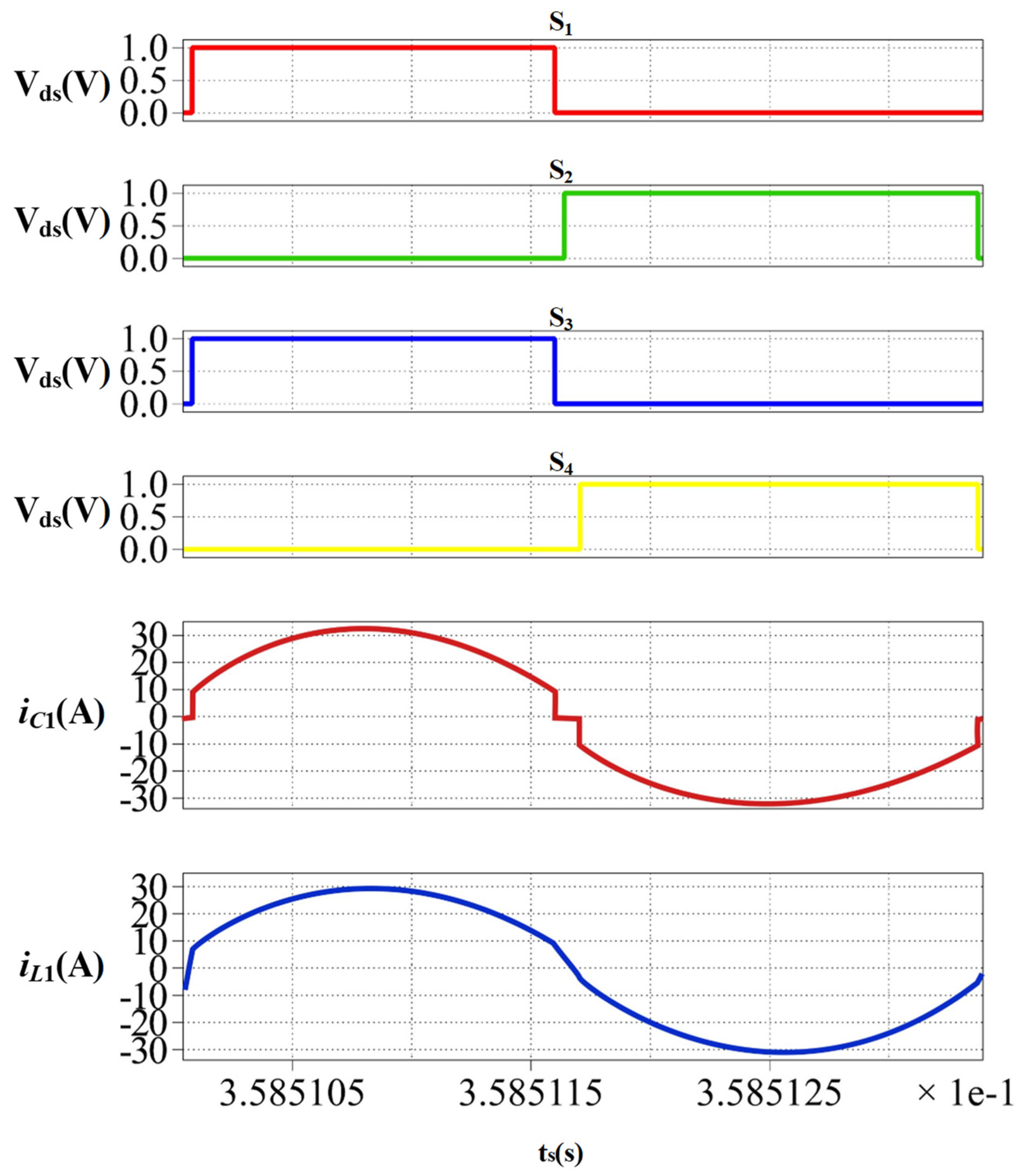
In order to verify the correctness of the theory proposed for solving the problem of mismatch between switching frequency and resonant frequency caused by differences in component parameters by adding an additional resonator, this paper uses the PLECS simulation software to build the relevant simulation model. The key simulation waveforms of the CVD(2:1) converter with multiple resonators are shown in Figure 8. From the simulation results, it can be observed that the voltage Vds borne by all the power devices in the CVD(2:1) converter is equal to the output voltage Vout. There is a certain dead zone between the power devices S1, S3 that are conducting in working mode 1 and the power devices S2, S4 that are conducting in working mode 2. Moreover, the dead zone interval between S4 and S1, S3 is longer. This is used to transfer the remaining energy in the resonant inductor to the output side. And within the set dead zone time, the resonant capacitor C2 in the additional resonator can resonate with the resonant inductor L1 in the main resonator, ensuring that the remaining energy stored in the inductor is transferred to the output end with minimal additional conduction losses.
Figure 8.
Key simulation waveform diagram of multi-resonator CVD(2:1) converter.
2.4. Design of the Multi-Resonant Circuit BUCK + CVD(2:1) POL Converter Prototype
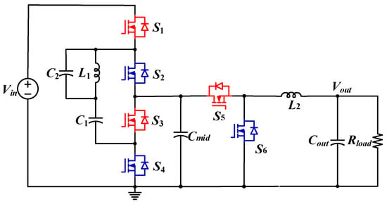
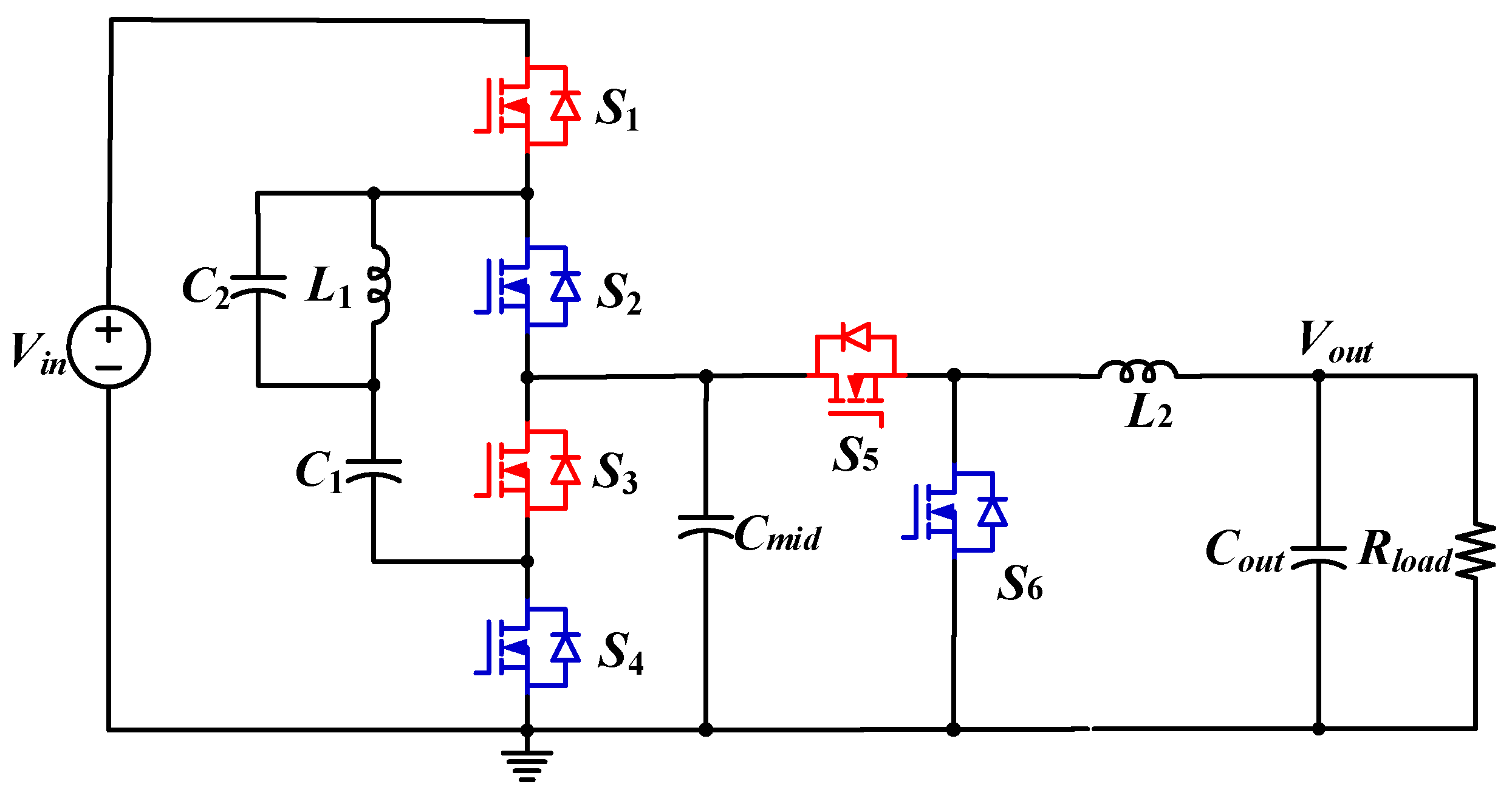
Based on the previous analysis, the new cascaded POL converter topology featuring robustness against component tolerances is shown in Figure 9.
Figure 9.
New multi-resonant BUCK + CVD(2:1) cascaded POL converter topology.
The design of the BUCK + CVD(2:1) converter prototype begins by selecting the main resonant frequency f0, which is determined by the parameters of the selected passive components. The calculation is shown in Equation (2).
In order to achieve the optimal soft-switching effect through the utilization of the additional resonant branch, the capacitance of the auxiliary resonant capacitor C2 must be strictly matched with the defined dead time. The fundamental design criterion requires that the total dead-time interval (tdead) must encompass exactly one-half of the oscillation period of the auxiliary resonant tank formed by L1 and C2. This ensures that the residual inductor current effectively reverses its direction before the next switching transition begins. Therefore, replacing arbitrary empirical ratios, the universal time-domain constraint for the dead time can be strictly expressed as:
where Tres2 represents the resonant period of the auxiliary branch. Based on this generalized physical boundary condition, once the necessary dead time is determined by the switching characteristics of the selected GaN devices, the optimal capacitance value for the additional resonant capacitor can be analytically derived as follows:
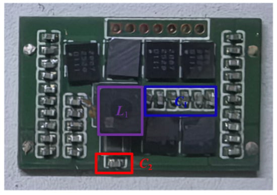
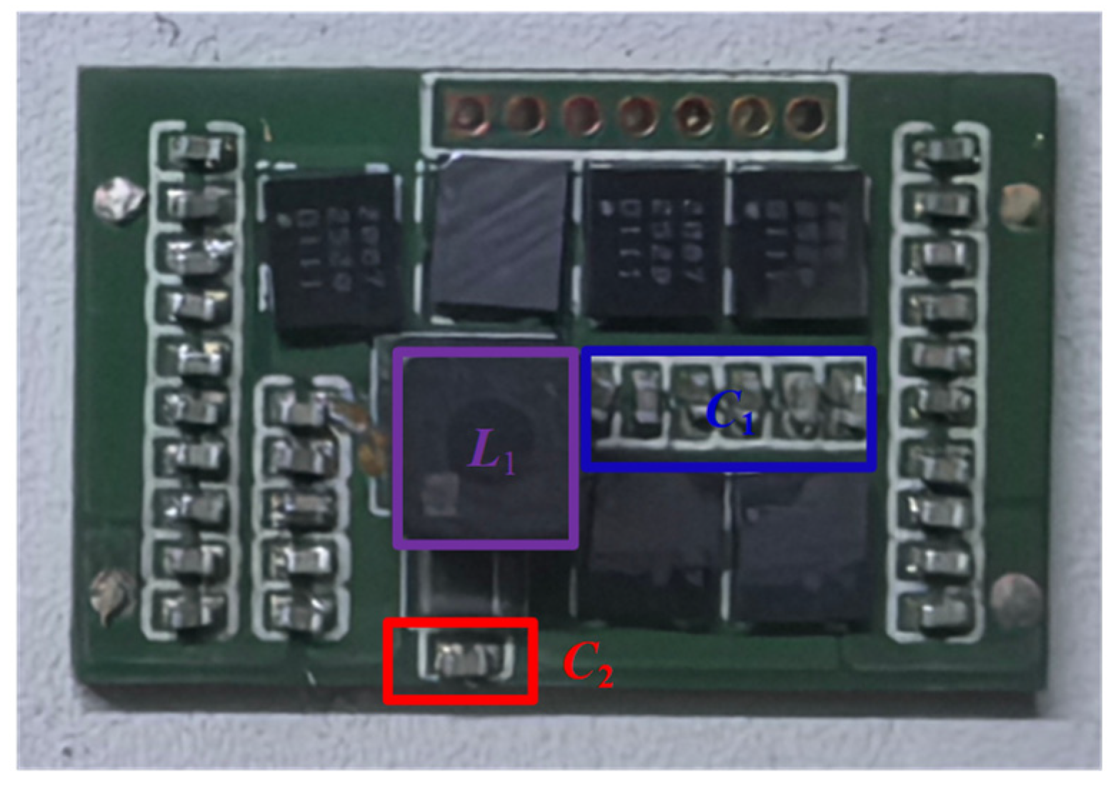
The prototype of the new multi-resonant circuit BUCK + CVD(2:1) converter is shown in Figure 10.
Figure 10.
The prototype of the new multi-resonant BUCK + CVD(2:1) cascaded POL converter.
3. Results
After completing the design of the multi-resonant circuit BUCK + CVD(2:1) cascaded POL converter prototype, in order to verify the correctness of the theory proposed for adding additional resonant branches to improve the insensitivity to frequency mismatch caused by variations in component parameters, relevant experiments are conducted on the multi-resonant circuit BUCK + CVD(2:1) cascaded POL converter prototype. The relevant experimental parameters are shown in Table 2, where the numbers in parentheses represent the quantity of the corresponding components.
Table 2.
Component specifications of the experimental prototype.
To ensure the accuracy and reproducibility of the experimental evaluation, the efficiency and transient response measurements were conducted using industry-standard test equipment. The input power was stably supplied by a Chroma 62000P programmable DC power supply (Chroma Ate Inc., Taoyuan City, Taiwan, China), while the output conditions were rigorously regulated using a Chroma 6310A programmable DC electronic load (Chroma Ate Inc., Taoyuan City, Taiwan, China). The voltage measurements were recorded utilizing a Fluke 17B+ digital multimeter (Fluke Corporation, Everett, WA, USA), providing a clear context for the overall measurement uncertainty. The test equipment models and test accuracies are listed in Table 3.
Table 3.
Table of experimental test equipment and accuracy specifications.
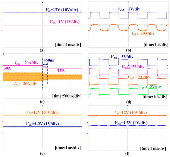
The relevant experimental waveforms of the multi-resonant circuit BUCK + CVD(2:1) cascaded POL converter prototype are shown in Figure 11.
Figure 11.
Experimental results of the new multi-resonant BUCK + CVD(2:1) cascaded POL converter. (a) input voltage Vin = 12 V and output voltage Vout = 1 V; (b) voltage waveform Vds2 of the GaN power switching device and the current waveform of the resonant inductor L1; (c) transient response (recovery time of 460 µs defined within a ±2%/±20 mV settling band); (d) drive voltage waveforms Vgs1, Vgs2, Vgs3 and Vgs4 of GaN power switching devices; (e) input voltage Vin = 12 V and output voltage Vout = 1.2 V; and (f) input voltage Vin = 12 V and output voltage Vout = 1.5 V.
Figure 11a shows that the input voltage is 12 V and the output voltage is 1 V. Figure 11b shows the voltage waveform of the drain-source voltage Vds2 of the GaN power switch device S2 and the current waveform iL1 flowing through the resonant inductor L1. The maximum drain-source voltage Vds2 on S2 is equal to the output voltage 1 V, and the waveform of the inductor circuit shows that when there is frequency mismatch, the second resonant branch resonates during the dead time, ensuring that the remaining energy in the inductor is transferred to the output side with minimum loss. Figure 11c shows the transient response capability of the multi-resonant circuit BUCK + CVD(2:1) type cascaded POL converter prototype. The output current is adjusted from 30 A to 15 A, and the response recovery time is 460 us (defined within a ±2%/±20 mV settling band). Figure 11d shows the voltage waveforms Vgs1, Vgs2, Vgs3, and Vgs4 of the GaN power switch devices S1, S2, S3, and S4. At the same time, in order to prove that the multi-resonant circuit BUCK + CVD(2:1) cascaded POL converter prototype still has excellent voltage regulation capability, after modifying the DSP program and reprogramming, the output voltage of the multi-resonant cascaded BUCK + CVD(2:1) type POL converter prototype is adjusted to 1.2 V and 1.5 V, respectively. The corresponding input and output voltage experimental waveforms are shown in Figure 11e,f.
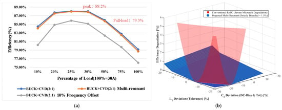
The measured efficiency curve of the multi-resonant BUCK + CVD(2:1) cascaded POL converter prototype is shown in Figure 12a. To prove the effectiveness of the additional resonant branch in solving the problem of component parameter differences, it is compared with the efficiency curve of BUCK + CVD(2:1) operating in the resonant mode and the efficiency curve under the condition where the working frequency is offset by 10% from the resonant frequency (simulating the condition of component parameter differences).
Figure 12.
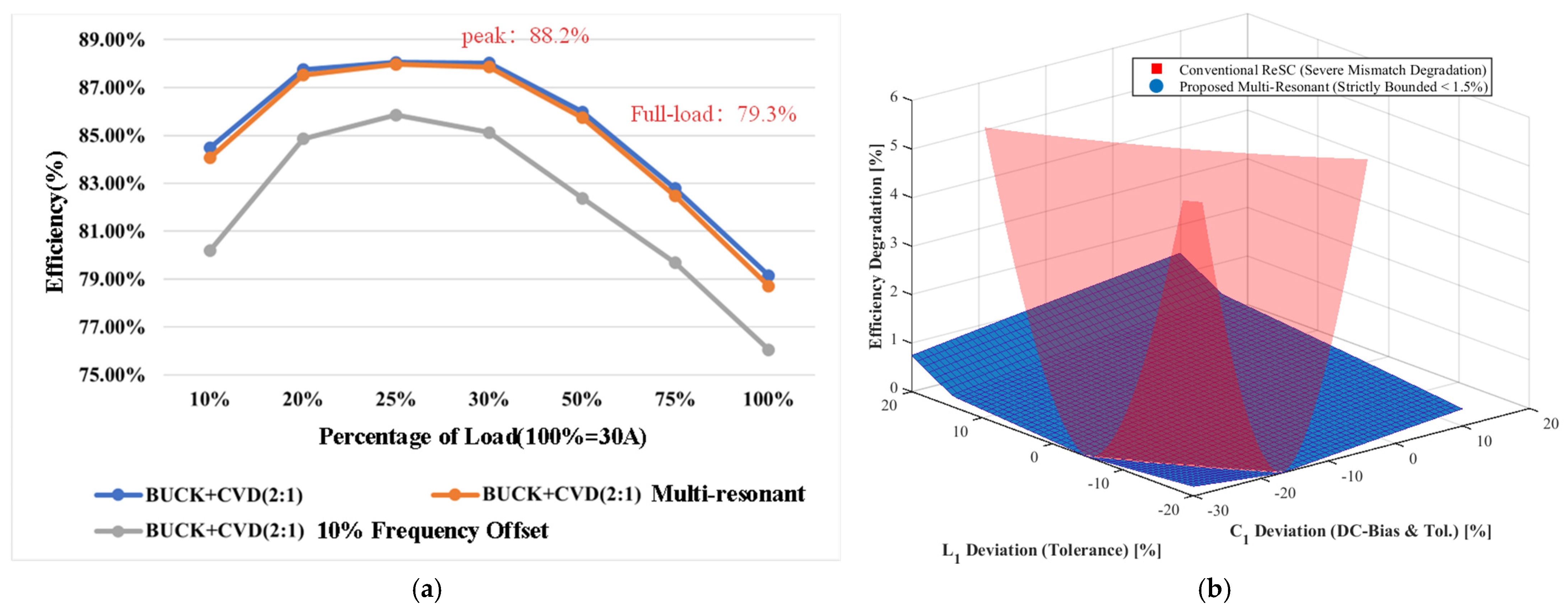
(a) The measured efficiency curve. (b) Multi-variable analytical sensitivity.
Figure 12b illustrates the system’s efficiency degradation when subjected to variations in C1 and L1. Conventional Topology (Red Surface): Highly sensitive to parameter mismatch. When parameters deviate, it loses zero-voltage switching (ZVS) and suffers massive hard-switching losses, causing the efficiency drop to surge steeply beyond 5.5%. Proposed Topology (Blue Surface): By utilizing the auxiliary capacitor C2 to absorb residual inductor energy during the dead time, it inherently maintains complete ZVS even under extreme 30% parameter drifts. As a result, the efficiency degradation is strictly clamped to under 1.5% (the flat blue basin), decoupling the switching frequency from strict hardware matching constraints.
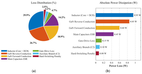
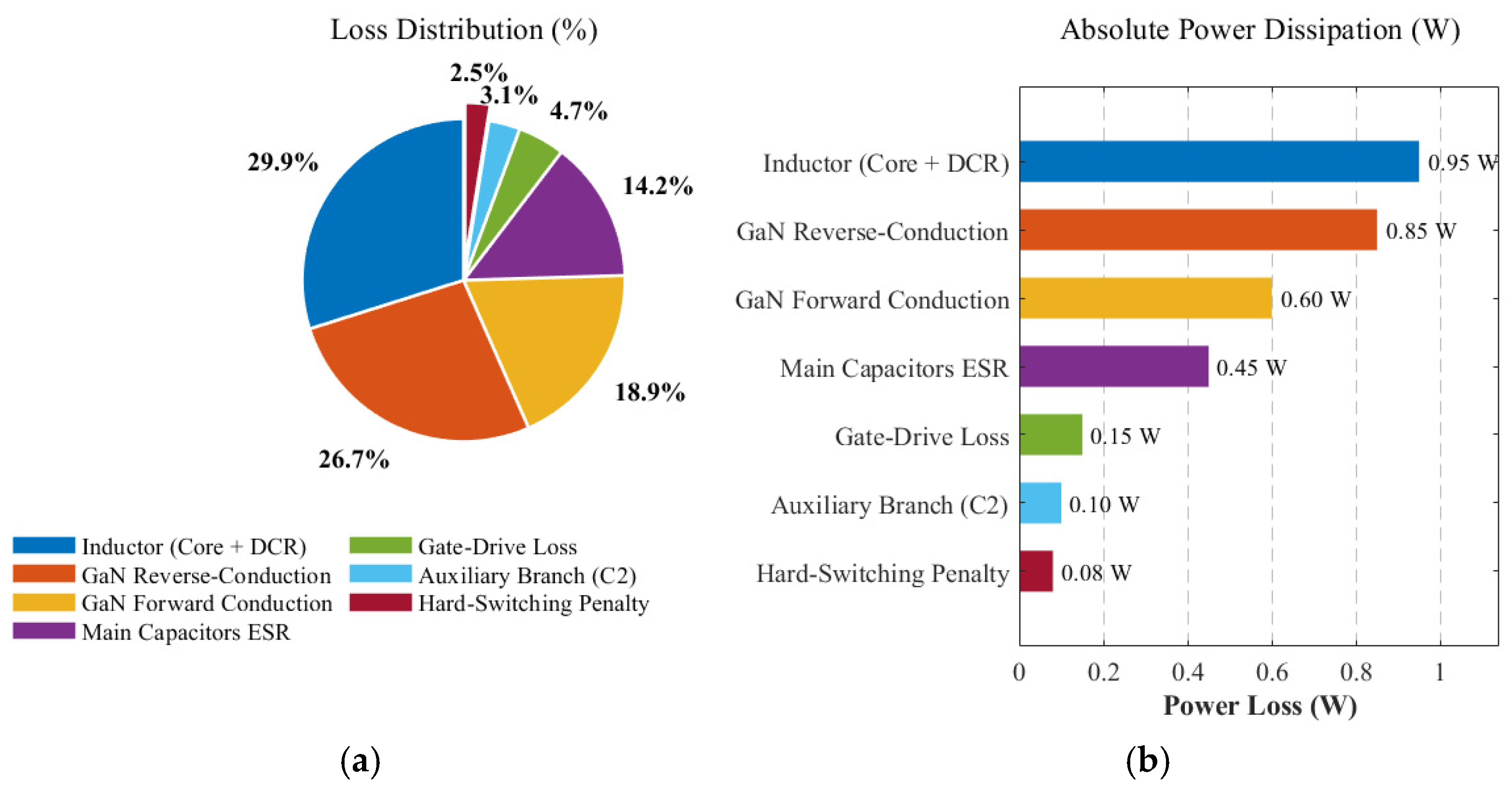
In Figure 13a, the hard-switching penalty is successfully clamped to merely 2.5% (<0.10 W). This verifies that the proposed auxiliary branch virtually eliminates turn-on losses even under severe mismatch conditions. However, as illustrated in Figure 13b, the total efficiency is still bounded by inherent component dissipations. The dominant factors are the inductor copper/core losses (0.95 W) and the GaN reverse-conduction losses (0.85 W). The significant reverse-conduction loss is a typical characteristic of enhancement-mode GaN devices due to their high voltage drop during the dead time. This breakdown explicitly clarifies that while the topology minimizes switching mismatch losses, it remains subject to standard physical conduction limits.
Figure 13.
Loss breakdown at 30 A under +20% parameter mismatch: (a) Percentage distribution; (b) Absolute power dissipation.
Dynamically, the converter exhibits strong transient regulation, achieving a 460 µs recovery time during a 50% load step (30 A to 15 A)—a marked improvement over conventional unmodulated ReSC converters. To establish a rigorous industrial benchmark, as quantified in Table 4, this 460 µs recovery time delivers a 2.5 times to 4 times speed-up compared with standard commercial mass-produced two-stage or cascaded telecom POL modules, which typically lag with a 1.2 ms to 1.8 ms settling boundary under identical high-current step disruptions.
Table 4.
Quantitative transient performance comparison with industrial mass-produced POL converters.
Furthermore, traditional synchronous BUCK converters heavily rely on maximizing closed-loop control bandwidth to suppress large voltage ripples, which inherently risks stability margins and induces a 6% to 10% voltage overshoot. In contrast, the proposed configuration utilizes the hardware-level multi-resonant tank to inherently buffer the transient charge mismatch during the dead-time intervals, clamping the empirical voltage overshoot to under 3% without complicating the localized DSP control loops, thereby presenting substantial dynamic superiority for high-current server applications.
4. Discussion
The proposed BUCK + CVD(2:1) cascaded POL converter effectively resolves the efficiency degradation typically caused by component parameter mismatches in indirect resonant switched-capacitor topologies. By introducing an auxiliary resonant branch, the prototype ensures virtually lossless energy transfer during the dead time, maintaining efficiency within 1% of the ideal condition even under a ±10% parameter variation typical of standard Class II ceramic capacitors. This robustness is achieved with minimal hardware overhead, requiring only a single standard 2.5 nF multi-layer ceramic capacitor, thus remaining fully compatible with automated surface-mount manufacturing with a bill of materials cost increase of less than 2%. Dynamically, the converter exhibits strong transient regulation, achieving a 460 µs recovery time during a 50% load step (30 A to 15 A)—a marked improvement over conventional unmodulated ReSC converters. Furthermore, while traditional synchronous BUCK converters rely on maximizing closed-loop bandwidth to suppress ripples—risking stability margins and inducing 6% to 10% voltage overshoots—the proposed configuration utilizes the hardware-level multi-resonant tank to buffer transient charge mismatch.
While the proposed converter has been rigorously validated against the conventional BUCK and standard CVD topologies through direct hardware implementation, comparisons with representative high-density industrial POL modules were conducted based on their published technical performance benchmarks. Due to the proprietary nature and high integration density of these commercial modules, direct hardware-level replication for side-by-side testing remains constrained. Nevertheless, the performance advantages demonstrated in transient recovery and mismatch robustness provide a clear objective benchmark for high-current data center power delivery architectures. While the multi-resonant mechanism significantly improves mismatch insensitivity, it requires precise gate-drive dead-time alignment to properly capture the auxiliary resonance. Addressing these practical physical constraints and integrating advanced thermal management designs will form the core focus of the next phase of this ongoing research trajectory. This includes developing parallel current-sharing control strategies to allow multiple cascaded POL units to collectively serve high-density microprocessor loads, further optimizing thermal distribution while preserving the fault-tolerant and high-efficiency characteristics demonstrated in this study.
5. Conclusions
This paper proposes a multi-resonant BUCK + CVD(2:1) cascaded point-of-load (POL) converter to address the high-density power demands of data centers. By introducing an auxiliary resonant branch, this topology effectively eliminates the efficiency degradation caused by switching and resonant frequency mismatches in conventional indirect resonant switched-capacitor converters. Experimental results from the 12 V-to-1 V/30 A GaN-based prototype confirm its robust performance. The converter maintains high efficiency even under a ±10% variation in passive component parameters. Furthermore, it exhibits a fast transient recovery time of 460 µs during a load step from 30 A to 15 A. Economically, the implementation requires only one additional 2.5 nF surface-mount capacitor, ensuring minimal manufacturing complexity and high feasibility for mass production.
While this multi-resonant mechanism enhances parameter variation insensitivity, it requires precise gate-drive timing during dead-time intervals. To bridge the gap toward practical industrial deployment, future research will focus on evaluating specific mass-production cost variations and scaling the passive components for higher power demands. Additionally, developing current-sharing control strategies for parallel module operations will be explored to optimize thermal management and ensure reliability under severe load faults.
Author Contributions
Conceptualization, D.B., Y.W. and X.L.; methodology, Y.W.; software, D.B.; validation, Y.W. and Q.C.; formal analysis, Q.C.; investigation, D.B.; resources, X.L.; data curation, Y.W.; writing—original draft preparation, Y.W.; writing—review and editing, D.B.; supervision, X.L.; project administration, X.L.; funding acquisition, X.L. All authors have read and agreed to the published version of the manuscript.
Funding
This research received no external funding.
Data Availability Statement
The data presented in this study are available on request from the corresponding author.
Conflicts of Interest
The authors declare no conflicts of interest.
Abbreviations
The following abbreviations are used in this manuscript:
| POL | Point-of-load |
| ReSC | Resonant switched-capacitor |
| CVD | Cascaded voltage divider |
| SC | Switched-capacitor |
| VCR | Voltage conversion ratio |
| ESR | Equivalent series resistance |
References
- Yun, W.; Trinh, P.-H.; Joo, J.-Y.; Chung, I.-Y. Coordinated Voltage and Power Factor Optimization in EV- and DER-Integrated Distribution Systems Using an Adaptive Rolling Horizon Approach. Energies 2025, 18, 6357. [Google Scholar] [CrossRef] [Scilit]
- Lyu, X.; Li, Y.; Ren, N.; Nan, C.; Cao, D.; Jiang, S. Optimization of High-Density and High-Efficiency Switched-Tank Converter for Data Center Applications. IEEE Trans. Ind. Electron. 2020, 67, 1626–1637. [Google Scholar] [CrossRef] [Scilit]
- Wang, C.; Gu, Y.; Li, H. Research on Coupled Inductor Interleaved High Step-Up DC-DC Converter. Energies 2025, 18, 6174. [Google Scholar] [CrossRef] [Scilit]
- Chen, Y.; Shi, K.; Chen, M.; Xu, D. Data Center Power Supply Systems: From Grid Edge to Point-of-Load. IEEE J. Emerg. Sel. Top. Power Electron. 2023, 11, 2441–2456. [Google Scholar] [CrossRef] [Scilit]
- Orabi, M.; Shawky, A. Proposed Switching Losses Model for Integrated Point-of-Load Synchronous Buck Converters. IEEE Trans. Power Electron. 2015, 30, 5136–5150. [Google Scholar] [CrossRef] [Scilit]
- Ge, T.; Ngo, K.D.T.; Moss, J. Two-Dimensional Gapping to Reduce Light-Load Loss of Point-of-Load Inductor. IEEE Trans. Power Electron. 2017, 32, 540–550. [Google Scholar] [CrossRef] [Scilit]
- Kumar, A.; Afridi, K.K. Single-stage isolated 48V-to-1.8V point-of-load converter utilizing an impedance control network for wide input range operation. In Proceedings of the 2017 IEEE Energy Conversion Congress and Exposition (ECCE), Cincinnati, OH, USA, 1–5 October 2017. [Google Scholar]
- Yang, R.; Li, Z.; Xie, Y.; Han, K.; Jin, Y.; Zeng, C. Research on the Invasive Measurement Method of System Harmonic Impedance Based on Capacitor Switching. In Proceedings of the 2023 2nd Asian Conference on Frontiers of Power and Energy (ACFPE), Chengdu, China, 27–29 October 2023; pp. 40–44. [Google Scholar]
- Le, H.-P.; Sanders, S.R.; Alon, E. Design Techniques for Fully Integrated Switched-Capacitor DC-DC Converters. IEEE J. Solid-State Circuits 2011, 46, 2120–2131. [Google Scholar] [CrossRef] [Scilit]
- Xu, X.; Guan, Y.; Wang, Y.; Xu, D. A Single-stage LLC Resonant GaN-based DC-DC Converter with Switched Capacitor. In Proceedings of the 2022 25th International Conference on Electrical Machines and Systems (ICEMS), Chiang Mai, Thailand, 29 November–2 December 2022; pp. 1–5. [Google Scholar]
- Ba, D.; Yu, F.; Wang, Y.; Chen, X.; Niu, Y.; Lyu, X. Optimization Study of Parasitic Parameters in Parallel Interleaved Windings for High-Frequency PCB Transformers. IEEE Trans. Power Electron. 2025, 40, 14894–14907. [Google Scholar] [CrossRef] [Scilit]
- Wai, V.; Ng, S.; Sanders, S.R. Switched Capacitor DC-DC Converter: Superior where the Buck Converter has Dominated. Doctoral Dissertation, Electrical Engineering and Computer Sciences Department of the University of California, Berkeley, CA, USA, 2011. [Google Scholar]
- Testa, R.A.; Abbas, M.Q.; Femia, A.; Vancini, L.; Rizzoli, G.; Mengoni, M.; Zarri, L.; Tani, A. A Theoretical Framework for the Control of Modular Multilevel Converters Based on Two-Time Scale Analysis. Energies 2025, 18, 6233. [Google Scholar] [CrossRef] [Scilit]
- Sahu, S.K.; Prasoon, S.; Gaurav, S.; Kumar, C. Operation and Control of Modular Multilevel DC-DC Converter for EV Charging Application. In Proceedings of the 2023 11th National Power Electronics Conference (NPEC), Guwahati, India, 14–16 December 2023; pp. 1–6. [Google Scholar]
- Lei, Y.; May, R.; Pilawa-Podgurski, R. Split-Phase Control: Achieving Complete Soft-Charging Operation of a Dickson Switched-Capacitor Converter. IEEE Trans. Power Electron. 2016, 31, 770–782. [Google Scholar] [CrossRef] [Scilit]
- Rizzolatti, R.; Mazzer, S.; Ursino, M.; Medeossi, E.; Seet, I.; Saggini, S.; Zufferli, K. Optimal Frequency Operating Points for Hybrid Switched Capacitor Converters and Lossless Current Sense Method. In Proceedings of the PCIM Europe 2024; International Exhibition and Conference for Power Electronics, Intelligent Motion, Renewable Energy and Energy Management, Nürnberg, Germany, 11–13 June 2024; pp. 2527–2532. [Google Scholar]
- Lei, Y.; Pilawa-Podgurski, R.C.N. Soft-charging operation of switched-capacitor DC-DC converters with an inductive load. In Proceedings of the 2014 IEEE Applied Power Electronics Conference and Exposition—APEC 2014, Fort Worth, TX, USA, 16–20 March 2014; pp. 2112–2119. [Google Scholar]
- Kesarwani, K.; Stauth, J.T. Resonant and multi-mode operation of flying capacitor multi-level DC-DC converters. In Proceedings of the 2015 IEEE 16th Workshop on Control and Modeling for Power Electronics (COMPEL), Vancouver, BC, Canada, 12–15 July 2015; pp. 1–8. [Google Scholar]
- Jong, O.; Li, Q.; Lee, F.C. Resonant Switched-Capacitor Converter with Multi-Resonant Frequencies. In Proceedings of the 2019 IEEE Applied Power Electronics Conference and Exposition (APEC), Anaheim, CA, USA, 17–21 March 2019; pp. 2177–2184. [Google Scholar]
- Ye, Z.; Lei, Y.; Pilawa-Podgurski, R.C.N. A resonant switched capacitor based 4-to-1 bus converter achieving 2180 W/in3 power density and 98.9% peak efficiency. In Proceedings of the 2018 IEEE Applied Power Electronics Conference and Exposition (APEC), San Antonio, TX, USA, 4–8 March 2018. [Google Scholar]
- Lei, Y.; Pilawa-Podgurski, R.C. A General Method for Analyzing Resonant and Soft-charging Operation of Switched-Capacitor Converters. IEEE Trans. Power Electron. 2014, 30, 5650–5664. [Google Scholar]
- Pasternak, S.R.; Kiani, M.H.; Rentmeister, J.S.; Stauth, J.T. Modeling and Performance Limits of Switched-Capacitor DC–DC Converters Capable of Resonant Operation with a Single Inductor. IEEE J. Emerg. Sel. Top. Power Electron. 2017, 5, 1746–1760. [Google Scholar] [CrossRef] [Scilit]
- Kesarwani, K.; Sangwan, R.; Stauth, J.T. Resonant-Switched Capacitor Converters for Chip-Scale Power Delivery: Design and Implementation. IEEE Trans. Power Electron. 2015, 30, 6966–6977. [Google Scholar] [CrossRef] [Scilit]
- Zhang, X.; Ma, Q.; Zhao, A.; Jiang, Y.; Law, M.-K.; Jiang, J.; Takamiya, M.; Martins, R.P.; Mak, P.-I. A 12/24 V-Input HV-LV-Separated Hybrid SC PoL Converter with 355 mW/mm3 Power Density at 3 A Load Current and 15.2 mm3 Power Passives. IEEE Trans. Power Electron. 2023, 38, 15109–15114. [Google Scholar] [CrossRef] [Scilit]
- Liu, Z.; Yuan, J.; Wu, F.; Cheng, L. A 12V/24V-to-1V PWM-Controlled DSD Converter with Delay-Insensitive and Dual-Phase Charging Techniques for Fast Transient Responses. IEEE J. Solid-State Circuits 2022, 57, 3853–3864. [Google Scholar] [CrossRef] [Scilit]
- Gong, M.; Chen, H.; Zhang, X.; Jain, R.; Raychowdhury, A. A 90.4% Peak Efficiency 48-to-1-V GaN/Si Hybrid Converter with Three-Level Hybrid Dickson Topology and Gradient Descent Run-Time Optimizer. IEEE J. Solid-State Circuits 2023, 58, 1002–1014. [Google Scholar] [CrossRef] [Scilit]
- Yan, D.; Yang, C.; Hang, L.; He, Y.; Luo, P.; Shen, L.; Zeng, P. Review of general modeling approaches of power converters. Chin. J. Electr. Eng. 2021, 7, 27–36. [Google Scholar] [CrossRef] [Scilit]

Disclaimer/Publisher’s Note: The statements, opinions and data contained in all publications are solely those of the individual author(s) and contributor(s) and not of MDPI and/or the editor(s). MDPI and/or the editor(s) disclaim responsibility for any injury to people or property resulting from any ideas, methods, instructions or products referred to in the content. |
© 2026 by the authors. Licensee MDPI, Basel, Switzerland. This article is an open access article distributed under the terms and conditions of the Creative Commons Attribution (CC BY) license.