


Abstract
This study examines the influence of device architecture and substrate materials on the external quantum efficiency (EQE) of high-performance solar cells. A diverse array of photovoltaic technologies was evaluated, including formamidinium lead iodide CH5N2PbI3 (FAPI) perovskite cells and various silicon-based designs, such as Passivated Emitter and Rear Cell (PERC), Back Integrated Contact (BIC), and Bifacial structures. Quantum characteristics were determined through wavelength-dependent photocurrent measurements utilizing a precision monochromator system. Our results reveal that device structure is a primary determinant of charge carrier collection efficiency; specifically, Bifacial and PERCs achieved superior short-circuit current densities (Jsc) of 40.98 mA/cm2 and 39.42 mA/cm2, respectively. Notably, the EQE(λ) profile of Bifacial cells under n-side illumination exhibits a near-ideal rectangular shape, indicating an optimized spectral response throughout the operating spectrum. Furthermore, the analysis investigates the role of surface recombination velocity and the efficacy of advanced passivation layers—specifically Al2O3 and SiNx—in enhancing quantum performance by mitigating recombination state density. Our findings demonstrate that the strategic integration of advanced passivation layers (Al2O3 and SiNx) with optimized architectures, such as PERC and Bifacial designs, is paramount for maximizing charge carrier collection and achieving record-high current densities reaching 40.98 mA/cm2. A comprehensive analysis of solar cell performance involves spectral response (SR) and external quantum efficiency (EQE) as functions of wavelength. Additionally, SR-based current density analysis enables more accurate evaluation of cell parameters than standard I–V characterization.
1. Introduction
The continuous evolution of photovoltaic (PV) technologies is fundamentally propelled by the dual imperative of enhancing conversion efficiencies and achieving cost-effective manufacturing. While crystalline silicon remains the dominant material in the PV market, innovative architectures such as Passivated Emitter and Rear Cell (PERC), Back Integrated Contact (BIC), and Bifacial structures have emerged to overcome the limitations of standard solar cells [1,2,3]. Simultaneously, perovskite solar cells, particularly those based on formamidinium lead iodide (FAPI), represent a promising frontier due to their exceptional optoelectronic properties and potential for high energy yield [4,5,6].
2. Experiment
The relationship between SR and EQE is fundamentally described by the following equation (where q is the elementary charge, λ is the radiation wavelength, h is Planck’s constant, and c is the speed of light [7,8,9,10]):
For a more detailed analysis of the effective light absorption, the internal quantum efficiency (IQE) is introduced, which accounts for the reflection losses described by the wavelength-dependent reflection coefficient, Rref(λ) [11,12].
Despite their fundamental significance, neither EQE nor IQE can be quantified through direct measurement; instead, they must be derived from wavelength-dependent photocurrent data. This study aims to provide a comparative analysis of the impact of device structure and material composition on the quantum characteristics of various PV technologies. By evaluating both laboratory-fabricated silicon and perovskite cells, as well as commercial references, this research investigates how different passivation strategies and layer configurations influence the spectral response and short-circuit current density (Jsc).
It is critical to underscore that deriving current parameters from SR/EQE measurements offers significantly higher precision than conventional current–voltage (I–V) characterization. This methodology facilitates the granular calculation of Jsc for discrete wavelength intervals, thereby providing an exhaustive assessment of device efficiency and carrier collection behavior across the solar spectrum.
External quantum efficiency can be expressed as
where J(λ) is the current density generated by the solar cell due to absorption of radiation at a given wavelength, and Nph(λ) is the incident photon flux, defined as the number of photons per unit area and time at a given wavelength [m−2/s·nm]. The photon flux is related to the incident optical power pin in the wavelength range from λ1 to λ2 through
When the analysis is focused on the radiation effectively absorbed by the cell, described by the factor (1 − Rref(λ)), where Rref(λ) is the wavelength-dependent reflection coefficient, the internal quantum efficiency (IQE) is introduced:
Combine the above relations with the following:
where Jsc denotes the short-circuit current density of the solar cell.
It is worth emphasizing that determining the cell current from SR/EQE measurements allows for greater precision than standard I–V characteristic measurements [1]. This method enables the precise calculation of the short-circuit current density (Jsc) for each wavelength range separately, which provides a more comprehensive overview of the device’s efficiency [4].
To accurately evaluate the overall impact of antireflective coatings or surface texturing on reflection reduction, the effective reflection coefficient Reff is commonly used. It is defined as [4]
Neither EQE nor IQE can be measured directly; instead, they are determined indirectly using Equations (2) and (4) [5]. In practice, the photocurrent generated by the tested solar cell Iph(λ) is measured as a function of wavelength. Simultaneously, the photocurrent of a calibrated reference photodiode Iph-diode(λ), with a known quantum efficiency EQEph-diode(λ), is recorded.
To evaluate these phenomena quantitatively, the external quantum efficiency is formally defined as the ratio of generated current density J(λ) to the incident photon flux Nph(λ):
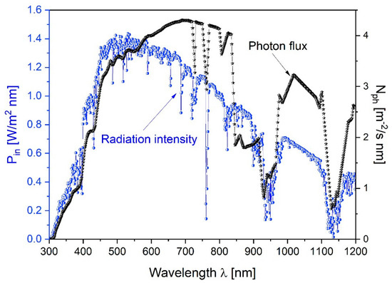
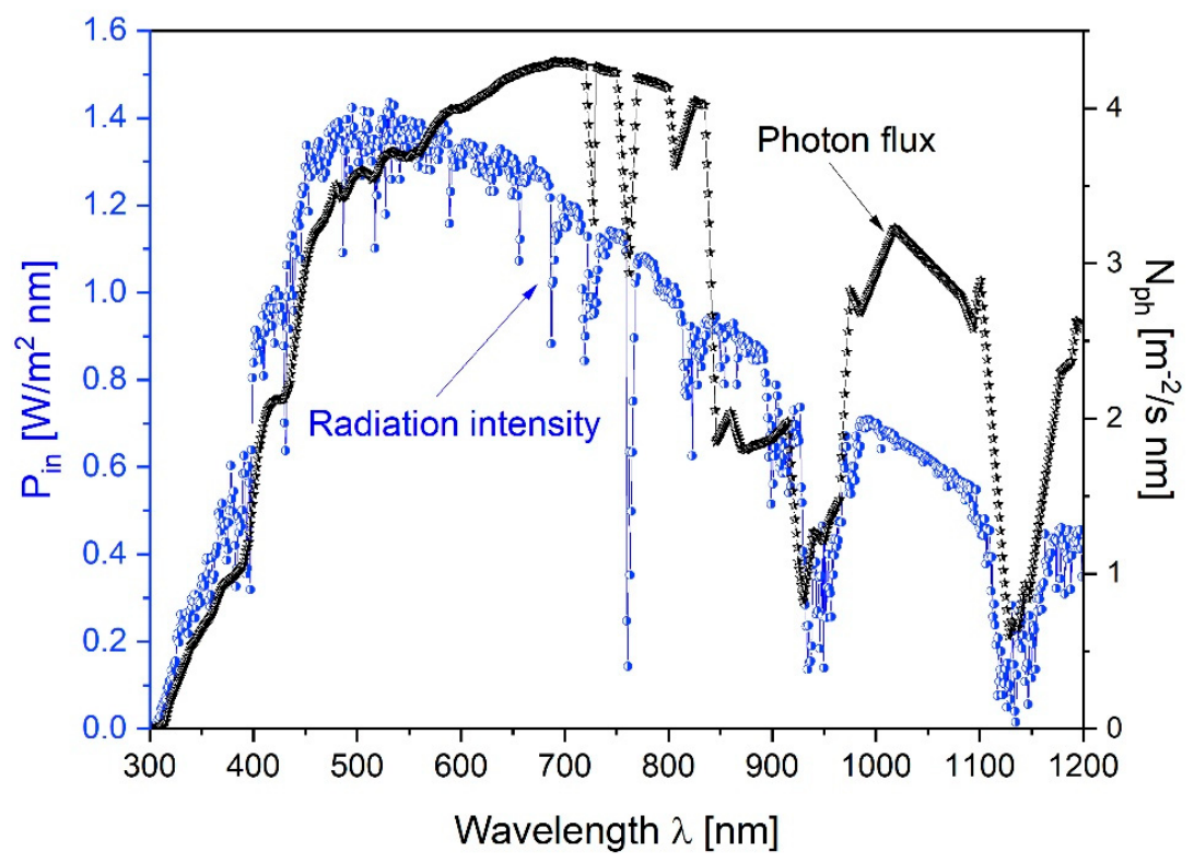
If the current-voltage (I–V) characteristics under AM1.5 illumination (Figure 1) are measured over a wavelength range of, for example, 300–1200 nm, the short-current density Jsc obtained from the I–V curve should correspond to the current density calculated from the integrated EQE spectrum according to Equation (2), which serves as an important consistency check of the measurements.
Figure 1.
AM1.5 radiation spectrum and photon flux for the above spectrum depending on the wavelength of radiation in the range of 300–1200 nm.
The abrupt decrease in photon flux in the 850–950 nm range is a characteristic feature of the standard AM1.5 solar spectrum, primarily caused by atmospheric water vapor absorption and the presence of molecular oxygen (O2) absorption lines (Fraunhofer lines), specifically the ‘y’ line (898.765 nm) and the ‘Z’ line (822.696 nm).
The EQE measurements were performed on a monochromator stand in the IMMS Photovoltaic Laboratory. Monochromator from the Photon Institute (Krakow, Poland) using a Czerny Turner configuration with two coated mirrors [9]. The spectral range and resolution are determined by installed diffraction gratings. The measurement system utilizes a monochromator with dual light source entrances, incorporating both Xenon and Halogen lamps to cover the UV to IR spectral range. Measurements were realized at a temperature of 25 ± 2 °C and humidity of 50 ± 15%. Lock-in signals were measured using an 8-channel, 24-bit, synchronous ADC converter ADS131E08IAG automatically selecting ranges of 100 mA, 10 mA, 1 mA, 10 µA, and 1 µA per 24 bits. This means the measurement accuracy for these ranges is 8.4 mA, 0.84 mA, 0.084 mA, 8.4 µA, and 84 nA, respectively.
The solar cells at IMMS were characterized by the light current–voltage (I–V) measurements at Solar Simulator SS200 AAA class EM Photo Emission Tech. Inc. (Moorpark, CA, USA) with Solar Cells I–V Curve Tracer SS I–V CT-02 PV. To ensure consistency measurement at the 800 nm transition point between the silicon (Hamamatsu Photonics, Shizuoka, Japan) and germanium (Thorlabs, Newton, NJ, USA) photodiodes, a calibration overlap was performed. This phenomenon does not affect the accuracy of the measurement data, as the system is calibrated using a reference silicon photodiode with known quantum efficiency, ensuring high consistency with certified Fraunhofer ISE data. The results from both sensors demonstrated high agreement at this wavelength, confirming the integrity of the combined spectral data. The data were obtained under AM1.5 global spectrum at 100 W/m2 light intensity at temperature of 25 °C. The reference cell No 005-2013 was calibrated at ISE Fraunhofer-Freiburg, Germany.
3. Results
The solar cells investigated during experiments are listed in Table 1. Metal contacts that cover only 3–5% of the cell surface are designated with the metal type PC, ‘partial coverage.’ This coverage was strictly accounted for in the calculation of current density relative to the active area of the cells. For other layers used exclusively for a given type of contact, the above designation is also used. Passivated emitter rear contact (PERC), passivated emitter rear locally diffused (PERL) and back integrated contact (BIC) are examples of silicon solar cell technologies that have made Bifacial solar cell operation a reality. Perovskite technology is promising and gaining research interest since it is less susceptible to self-heating and produces more energy.
Table 1.
The solar cells were investigated experimentally. The short circuit current density Jsc value given in the table was calculated from EQE according to Formula (5). Note: The symbols and abbreviations in the ‘Symbol’ column are used as unique identifiers for each solar cell type in all subsequent figures.
The Fraunhofer n-type Si 5-2013 is ISE Fraunhofer monocrystalline Cz-Si n-type reference solar cell with certificate number ID 005-2013 fully encapsulated with 4 cm2 surface. The data delivered by ISE were obtained under reference spectrum AM 1.5 G IEC60904-3Ed.2 with irradiance 1000 W/m2 at temperature 25 °C. The full encapsulation of the Fraunhofer n-type Si 5-2013 significantly influences its optical coupling, as the protective layers affect both light reflection and transmission, which is directly reflected in the final registered photocurrent value. The I–V characteristic data for 7 PERC Si are enclosed according to data given by Haibing Huang [10].
The photovoltaic performance parameters extracted from the light current–voltage (I–V) characteristic curves under standard test conditions (AM1.5, 1000 W/m2) are summarized in Table 2 [1,7]. The data highlights the technological superiority of the PERC architecture, which achieved the highest conversion efficiency of 20.68% and a short-circuit current density (Jsc) of 39.43 mA/cm2, significantly surpassing the performance of the Classic Cell Si [2].
Table 2.
The results are extracted from light I–V characteristic curves.
Furthermore, to verify the operational current and conversion efficiency under conditions resembling actual device operation, steady-state power output measurements were performed. The results of this analysis confirm the stability of the generated power over time and provide additional validation for the operational current and efficiency summarized in Table 2, ensuring that the reported parameters are representative of the cells’ performance in a steady state.
The data summarized in Table 2 confirm the advantage of SR analysis over general I–V measurements [1,2]. Due to the division of the spectrum into 50 nm intervals, it is possible to precisely compare the contribution of specific wavelength ranges to the total current density for various cell structures, such as PERC and Bifacial [3]. This allows for the identification of specific spectral regions where a given material or structure exhibits its highest efficiency [4,6].
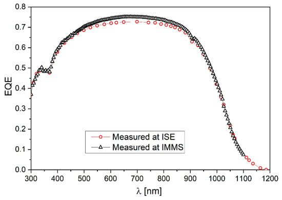
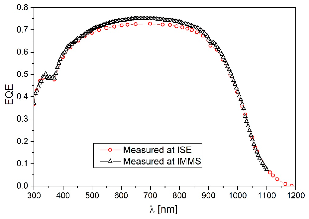
To validate the accuracy of the measurement system, the EQE characteristics for the reference Fraunhofer n-type Si 5-2013 cell were measured and compared with the certified data provided by ISE Fraunhofer. As shown in Figure 2, the experimental results obtained at IMMS demonstrate high consistency with the reference values [7]. After calculating the short-circuit current density (Jsc) according to Formula (5), the difference between the results obtained at IMMS and ISE was determined to be 1.96%, which is within the ±2% error range specified for the Fraunhofer reference cell [1,7].
Figure 2.
Comparison of EQE data for Fraunhofer n-type Si 5-2013 cell measured at ISE Fraunhofer and IMMS Krakow.
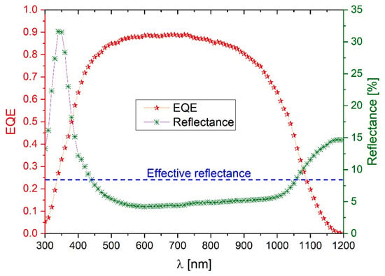
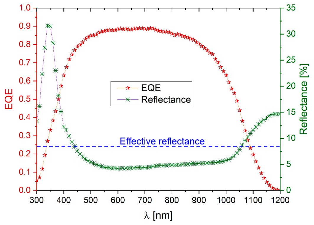
After calculating the current density Jsc from EQE measurements according to Formula (5), the difference between the results obtained in IMMS and ISE is 1.96% which is within the error range of ±2% given in specification of the Fraunhofer n-type Si 5-2013 solar cell. Classic Cell Si was fabricated with TiO2 as an antireflective coating according to the procedure elaborated at Photovoltaics Laboratory in IMMS [6]. The dependence of EQE and reflectance on wavelength for this cell is illustrated in Figure 3 [7].
Figure 3.
The dependence of EQE and reflectance on wavelength for Classic Cell Si. The effective reflectance (Eff) in the range of 300–1200 nm is 8.17%.
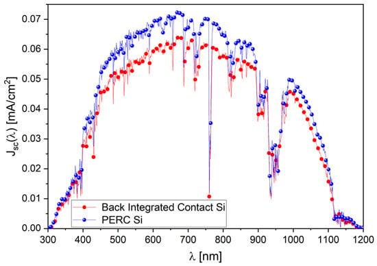
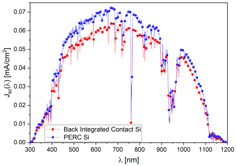
Back Integrated Contact Si solar cells have the front and back contacts located together on the rear surface, reducing to zero contact shading on the front. The industrial PERC solar cell with overall structure Ag (PC)/SiNx-ARC/n+Si/p-Si/p+Si/Al2O3/SiNx/Al (PC) has the front Ag-based contact fired through SiNx-ARC directly to n+ Si emitter and back Al contact is similarly metallized with p+ Si [10]. The spectral distribution of the current density Jsc(λ) for both BIC and PERCs is compared in Figure 4.
Figure 4.
Dependence of the current density distribution on the wavelength for Back Integrated Contact Si and PERC Si.
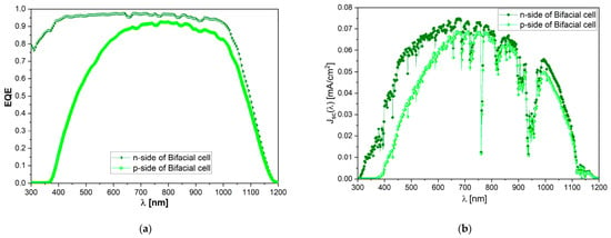
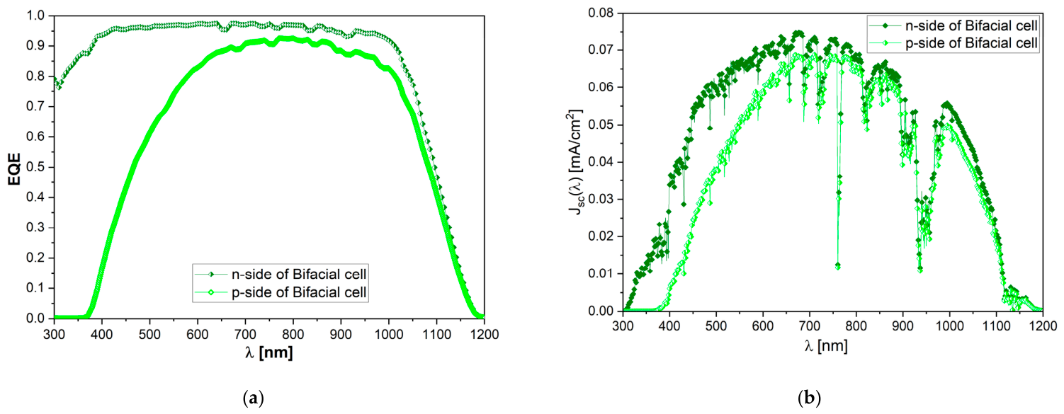
Bifacial solar cells (BSC) can simultaneously collect direct and albedo radiation reaching both the front and back side of a cell. Because the aluminum back metallization is eliminated by reducing infrared absorption, the decrease in cell working temperature leads to additional increases in maximum power output [6]. They are more applicable to an east–west-oriented PV installation or in city environments, where reflection from concrete–glass walls is significant. In the case of Bifacial solar cells, the measurement was performed in two steps, firstly on side n (Bifacial Si n-side) and next on side p (Bifacial Si p-side). The spectral dependence of EQE and the current density distribution Jsc(λ) for both illumination sides are illustrated in Figure 5.
Figure 5.
(a) Spectral dependence of EQE and (b) Jsc on wavelength for Bifacial cell measured on illuminated one side—n (Bifacial Si n-side) or p (Bifacial Si p-side).
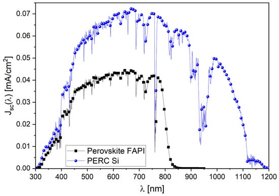
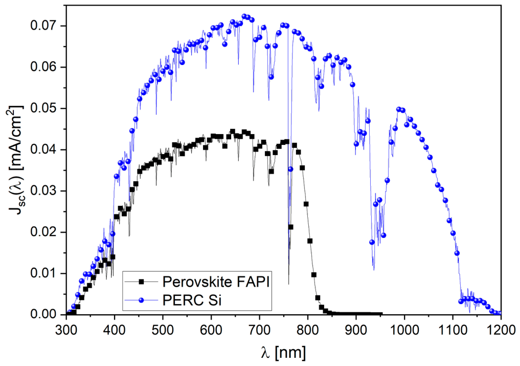
The perovskite FAPI (n-i-p) solar cell No. 5 was prepared on a fluorine-doped tin oxide (FTO) glass. Next, blocking titanium dioxide (TiO2) layer and mesoporous (mp) titanium thin TiO2 layer were spincoated. The FAPI perovskite layer was spin-coated on this FTO/TiO2/mp-TiO2 substrate and heated to ensure the formation of the black-colored FAPI phase. A 2,2′,7,7′-Tetrakis [N,N-di(4-methoxyphenyl) amino]-9,9′-spirobifluorene (Spiro-OMeTAD) film was used as a hole-transporting layer. The whole process was completed by the deposition of a gold electrode [3]. The comparison of the spectral current density distribution Jsc(λ) for the Perovskite FAPI cell (No. 5) and the PERC Si cell is illustrated in Figure 6.
Figure 6.
Dependence of the current density distribution on the wavelength for the Perovskite FAPI cell and PERC Si.
To provide a deeper insight into the spectral performance of the investigated devices, the photocurrent contribution from specific wavelength intervals was analyzed. The data summary of the current density values generated by each cell in 50 nm radiation wavelength ranges, calculated from the EQE results according to Formula (2) for AM1.5 conditions, is presented in Table 3. This detailed distribution confirms that the superior performance of the Bifacial Si (n-side) cell is primarily due to its high collection efficiency in the visible and near-infrared regions, specifically reaching a peak value of 3.578 mA/cm2 in the 551–600 nm range.
Table 3.
The data summary of the current density values generated by the cell in each radiation wavelength range calculated from the EQE measurement results after multiplying by the photon flux Nph(λ) for AM1.5 conditions and elementary charge q value according to Formula (2).
The highest photocurrent density value of 3.578 mA/cm2 in the 50 nm wavelength range can be obtained from the Bifacial Si n-side solar cell, i.e., measured from the n-type emitter side.
The short-circuit current density (Jsc) values presented in Table 1, which were calculated from EQE measurements [1], and the values in Table 2, derived from light I–V characteristics [2], show high consistency, serving as an important validation of the experimental setup [3,4]. A detailed breakdown of the photocurrent contribution from specific wavelength intervals, illustrating how material composition and structure influence carrier collection across the spectrum, is provided in Table 3 [5,6]. This approach integrates the data from the various tables into a logical framework and underscores the rigorous verification of the results against the certified Fraunhofer reference cell, which yielded a high level of consistency within 1.96% [4].
The slight discrepancies in the Jsc values for the PERC Si solar cell reported in Table 1, Table 2 and Table 3 arise from differences in the applied methodologies, namely direct I–V measurements, integration of the continuous EQE spectrum, and summation over discrete spectral intervals (50 nm), respectively. Such variations are methodologically expected and fall within the normal range of measurement uncertainty, thereby confirming the consistency and reliability of the obtained result.
4. Results and Discussion—Surface Recombination Effects on EQE
4.1. Impact of Surface Recombination and Passivation Mechanisms
The analysis of spectral response (SR) provides a more granular understanding of charge carrier dynamics compared to integrated current–voltage (I–V) measurements. Specifically, the ability to derive within discrete spectral intervals is instrumental in identifying how physical phenomena, such as surface recombination, curtail the collection efficiency in various device layers [6,7].
Experimental data and PC1D simulations demonstrate that surface recombination remains a critical bottleneck for external quantum efficiency (EQE), particularly in the short-wavelength regime (300–500 nm) [4]. The high density of recombination centers at the Si lattice boundary (1 × 1013 cm−2) was effectively mitigated through the application of advanced passivation stacks, as evidenced by the significant EQE enhancement in the short-wavelength regime (300–500 nm) for our PERC and Bifacial samples [5,9]. These defects lead to a reduction in charge carrier concentration near the surface and cause the bending of energy band edges—upwards for n-type or downwards for p-type semiconductors—to satisfy condition of constant Fermi energy [6,8,10].
The recombination process occurs through levels in the forbidden energy band: fast states at the semiconductor–oxide boundary (with equilibrium established in ~10−8 s) and slow states within the passivating layer itself [8,14]. For non-passivated Si surfaces, the number of recombination centers (Nit) is approximately 1 × 1013 cm−2 [8,9]. Simulations performed using the PC1D program for the Classic Cell Si confirmed that for high surface recombination velocities (S = 105–107 cm/s), there is a drastic drop in EQE for photons absorbed near the surface [3,4,6,10].
To mitigate these losses, advanced passivation layers such as Al2O3 and SiNx are implemented to saturate incomplete bonds [7,11,12]. While SixNy:H is suitable for n-type Si due to its positive Qf charge, Al2O3 (deposited via ALD) provides excellent passivation for p-type surfaces through a high negative fixed charge (Qf) [9,14,15,16]. These mechanisms explain the superior short-wavelength response observed in the PERC and Bifacial structures compared to the classic configuration [3,4,6,12]. Specifically, as shown in Table 3, the PERC Si cell achieves a photocurrent density of 0.805 mA/cm2 in the 301–350 nm interval compared to 0.496 mA/cm2 for the Classic Cell Si; this 62.3% enhancement in the short-wavelength region directly correlates with the reduced surface recombination velocity afforded by the Al2O3 passivation layer used in our PERC architecture.
For a standard silicon cell with an 80 Ω/□ emitter, the front surface recombination velocity (SRV) primarily determines the carrier collection probability before they reach the p-n junction [1]. At high SRV values (typically 105 to 107 cm/s for non-passivated surfaces), a high density of recombination states (Dit) at the silicon interface leads to a substantial loss of high-energy photons absorbed near the surface [7].
4.2. Comparative Analysis of Device Architectures
The comparative analysis reveals that while device architecture dictates the overall collection probability, material-specific absorption limits—particularly in the infrared region for FAPI perovskites—remain the primary constraint on total quantum performance compared to silicon-based benchmarks [2,14]. The key findings of this study are summarized as follows:
- Superiority of Advanced Silicon Architectures: Both Bifacial (n-side) and PERCs achieved the highest short-circuit current densities, reaching 40.98 mA/cm2 and 39.42 mA/cm2, respectively [2,3]. The Bifacial cell, when illuminated from the n-side, exhibited an EQE profile closest to an ideal rectangular shape, indicating exceptionally efficient charge carrier collection across a broad spectral range [3,6].
- Influence of Contact Geometry: BIC architecture, while eliminating front-side shading, showed lower spectral response compared to PERC, highlighting that optimizing the internal passivation and emitter profile is as critical as minimizing optical shading [2]. While the BIC architecture eliminates front-side shading, the front metallization in PERC, Bifacial, and Classic Cell Si covers approximately 3–5% of the surface area. To account for this partial coverage (PC), all Jsc values were normalized to the actual active area, enabling a consistent comparison of quantum performance.
- Impact of Device Encapsulation on Optical and Current Parameters: The comparative analysis also accounts for the influence of the encapsulation approach on solar cell performance. Full encapsulation, exemplified by the Fraunhofer reference cell (Fraunhofer n-type Si 5-2013), significantly alters the optical coupling of the device by affecting both light reflection and transmission at the protective interfaces. This factor is essential when evaluating the performance of certified, fully protected devices against non-encapsulated experimental laboratory structures, as the encapsulation layer directly influences the absolute density of the generated photocurrent.
- Silicon vs. Perovskite FAPI Performance: Although perovskite FAPI cells represent a promising technology due to their potential energy yield, their current spectral response (reaching a Jsc of 16.16 mA/cm2) remains significantly limited in the infrared region compared to silicon-based devices [2,3,12].
- Methodological Validation: The precision of our monochromator-based measurement system at IMMS is confirmed by a minimal deviation of 1.96% from the certified Fraunhofer reference standards, ensuring that even granular current variations in the nanoampere range are accurately captured [15,16]. The lower EQE values observed in the 300–750 nm range, as reflected in the Jsc data in Table 3, are attributed to the current stage of laboratory development, necessitating ongoing advancements in interface optimization to match optimized literature benchmarks.
5. Conclusions
In conclusion, this study demonstrates that the transition from conventional silicon architectures to advanced configurations, such as PERC and Bifacial cells, is a fundamental prerequisite for maximizing photovoltaic conversion efficiency [1]. Our experimental findings reveal that device architecture and material composition serve as the primary determinants of quantum performance [2]. Specifically, the Bifacial (n-side) and PERC structures demonstrated superior performance, achieving short-circuit current densities (Jsc) of 40.98 mA/cm2 and 39.42 mA/cm2, respectively.
The research underscores the pivotal role of advanced passivation strategies in mitigating surface recombination losses [1,17,18]. The implementation of Al2O3 and SiNx layers was shown to effectively reduce the density of recombination states, thereby broadening the spectral response across a wider wavelength range [4]. Notably, the near-ideal rectangular EQE profile observed in Bifacial cells under n-side illumination serves as a benchmark for optimized light management and exceptionally efficient charge carrier collection [4,5,6,7].
A significant methodological contribution of this work is the validation of spectral response-based analysis as a superior diagnostic tool. We have shown that SR-based current density analysis provides a more granular and accurate evaluation of cell parameters than standard I–V characterization [8,9]. The reliability of this approach is rigorously confirmed by the high level of consistency (within 1.96%) achieved between the measurements conducted at IMMS and the certified Fraunhofer reference cell [10].
Furthermore, while emerging perovskite FAPI technologies exhibit significant potential for high energy yields, their current performance remains limited in the infrared spectrum compared to silicon-based benchmarks [7,12]. This discrepancy, particularly in the visible spectral range, highlights the necessity for ongoing advancements in bandgap engineering and interface optimization to enhance carrier collection efficiency [12]. This study establishes a rigorous diagnostic framework utilizing spectral response analysis to pinpoint efficiency bottlenecks, demonstrating that interface optimization is more critical than optical shading reduction for next-generation silicon and perovskite architectures [1,13].
Author Contributions
Conceptualization, M.M.-S.; methodology, M.M.-S.; validation, M.M.-S. and P.P.; formal analysis, M.M.-S.; investigation, M.M.-S. and B.S.; investigation, P.P. and K.G.-N.; resources, B.S. and C.M.; data curation, M.M.-S.; writing—original draft preparation, M.M.-S.; writing—review and editing, M.M.-S.; visualization, M.M.-S.; supervision, M.M.-S.; project administration, M.M.-S.; funding acquisition, C.M. All authors have read and agreed to the published version of the manuscript.
Funding
This publication is co-funded by the Institute of Metallurgy and Materials Science of the Polish Academy of Sciences within the statutory work Z-13/2026.
Data Availability Statement
The original contributions presented in this study are included in the article. Further inquiries can be directed to the corresponding author.
Acknowledgments
The authors acknowledge the use of generative AI tools. OpenAI’s ChatGPT (OpenAI, San Francisco, CA, USA) was employed solely for language editing, grammar correction, and improvement of text readability. This tool was not used for generating scientific results, data analysis, interpretation of findings, or drawing scientific conclusions. All AI-generated outputs were carefully reviewed, verified, edited, and approved by the authors. The authors take full responsibility for the accuracy, integrity, and scientific validity of all content included in the manuscript. The authors confirm that no copyrighted third-party material was knowingly reproduced through the use of this too.
Conflicts of Interest
The authors declare no conflict of interest.
References
- Sze, S.M. Physics of Semiconductor Devices; John Wiley & Sons: Hoboken, NJ, USA, 1998. [Google Scholar]
- Sahayaraj, S.; Starowicz, Z.; Ziółek, M.; Socha, R.; Major, Ł.; Góral, A.; Gawlińska-Nęcek, K.; Palewicz, M.; Sikora, A.; Piasecki, T.; et al. Synergistic Effect of Precursor and Interface Engineering Enables High Efficiencies in FAPbI3 Perovskite Solar Cells. Materials 2023, 16, 5352. [Google Scholar] [CrossRef] [Scilit] [PubMed]
- Kot, M.; Gawlińska-Nęcek, K.; Pożarowska, E.; Henkel, K.; Schmeißer, D. Photosensitivity and Carrier Densities of Perovskite Solar Absorbers. Adv. Sci. 2025, 12, 2412711. [Google Scholar] [CrossRef] [Scilit] [PubMed]
- Menna, P.; Di Francia, G.; La Ferrara, V. Porous Silicon in Solar Cells: A Review and a Description of Its Application as an AR Coating. Sol. Energy Mater. Sol. Cells 1995, 37, 13–24. [Google Scholar] [CrossRef] [Scilit]
- Sze, S.M.; Li, Y.; Ng, K.K. Physics of Semiconductor Devices, 4th ed.; Wiley: Hoboken, NJ, USA, 2021. [Google Scholar]
- Panek, P.; Drabczyk, K.; Zięba, P. Crystalline silicon solar cells with high resistivity emitter. Opto-Electron. Rev. 2009, 17, 161–165. [Google Scholar] [CrossRef]
- Arora, N.A.; Hauser, J.R. Spectral Response of n+-n-p and n+-p Photodiodes. IEEE Trans. Electron Devices 1984, 31, 430–434. [Google Scholar] [CrossRef] [Scilit]
- Guerrero-Lemus, R.; Vega, R.; Kim, T.; Kimm, A.; Shephard, L.E. Bifacial solar photovoltaics—A technology review. Renew. Sustain. Energy Rev. 2016, 60, 1533–1549. [Google Scholar] [CrossRef] [Scilit]
- Siefer, G.; Gandy, T.; Schachtner, M.; Wekkeli, A.; Bett, A.W. Improved Grating Monochromator Set-Up for EQE Measurements of Multi-Junction Solar Cells. In Proceedings of the 39th IEEE Photovoltaic Specialists Conference (PVSC), Tampa, FL, USA, 16–21 June 2013; pp. 1740–1743. [Google Scholar] [CrossRef] [Scilit]
- Huang, H.; Lv, J.; Bao, Y.; Xuan, R.; Sun, S.; Sneck, S.; Li, S.; Modanese, C.; Savin, H.; Wang, A.; et al. 20.8% industrial PERC solar cell: ALD Al2O3 rear surface passivation, efficiency loss mechanisms analysis and roadmap to 24%. Sol. Energy Mater. Sol. Cells 2017, 161, 14–30. [Google Scholar] [CrossRef] [Scilit]
- Dullweber, T.; Kranz, C.; Peibst, R.; Baumann, U.; Hannebauer, H.; Fülle, A.; Steckemetz, S.; Weber, T.; Kutzer, M.; Müller, M.; et al. PERC+: Industrial PERC solar cells with rear Al grid enabling bifaciality and reduced Al paste consumption. Prog. Photovolt. Res. Appl. 2015, 24, 1487–1498. [Google Scholar] [CrossRef] [Scilit]
- Schmidt, J.; Merkel, A.; Brendel, R.; Hoex, B.; van de Sanden, M.C.M.; Kessels, W.M.M. Surface Passivation of High-efficiency Silicon Solar Cells by Atomic-layer-deposited Al2O3. Prog. Photovolt. Res. Appl. 2008, 16, 461–466. [Google Scholar] [CrossRef] [Scilit]
- Kopecek, R.; Buchholz, F.; Mihailetchi, V.D.; Libal, J.; Lossen, J.; Chen, N.; Chu, H.; Peter, C.; Timofte, T.; Halm, A.; et al. Interdigitated Back Contact Technology as Final Evolution for Industrial Crystalline Single-Junction Silicon Solar Cell. Solar 2023, 3, 1–14. [Google Scholar] [CrossRef] [Scilit]
- Schiele, Y.; Brinkmann, N.; Hahn, G.; Terheiden, B. Comparison of bifacial and monofacial large area n-type Si solar cells from 100 µm thin wire-sawn wafers. In Proceedings of the 31st European Photovoltaic Solar Energy Conference and Exhibition, Hamburg, Germany, 14–18 September 2015; pp. 399–403. [Google Scholar]
- Figielski, T. Zjawiska Nierównowagowe w Półprzewodnikach (Non-Equilibrium Phenomena in Semiconductors); PWN: Warszawa, Poland, 1980. [Google Scholar]
- Vermang, B.; Rothschild, A.; Racz, A.; John, J.; Poortmans, J.; Merens, R.; Poodt, P.; Tiba, V.; Roozeboom, F. Spatially separated atomic layer deposition of Al2O3, a new option for high-throughput Si solar cell passivation. Prog. Photovolt. Res. Appl. 2011, 19, 733–739. [Google Scholar] [CrossRef] [Scilit]
- Bőer, K.W. Survey of Semiconductor Physics; Van Nostrand Reinhold: New York, NY, USA, 1992. [Google Scholar]
- Aberle, A.G. Crystalline Silicon Solar Cells—Advanced Surface Passivation and Analysis; Centre for Photovoltaic Engineering UNSW: Sydney, Australia, 1999. [Google Scholar]

Disclaimer/Publisher’s Note: The statements, opinions and data contained in all publications are solely those of the individual author(s) and contributor(s) and not of MDPI and/or the editor(s). MDPI and/or the editor(s) disclaim responsibility for any injury to people or property resulting from any ideas, methods, instructions or products referred to in the content. |
© 2026 by the authors. Licensee MDPI, Basel, Switzerland. This article is an open access article distributed under the terms and conditions of the Creative Commons Attribution (CC BY) license.