


Abstract
The inductively coupled plasma (ICP) etching of deep trenches in InP was studied systematically with two gas mixtures, Cl2/CH4/H2 and Cl2/Ar. In the first mixture the sidewall profile was controlled through the CH4 and H2 flows. The optimized conditions were radio-frequency (RF) and ICP powers of 120 and 400 W, Cl2/CH4/H2 flow rates of 8/10/5 sccm (standard cubic centimeters per minute), a lower-electrode set temperature of 30 °C and a chamber pressure of 4 mTorr (millitorr). In the second mixture the Cl2/Ar flow ratio was used to balance chemical etching, ion bombardment and surface deposition. The optimized conditions were RF and ICP powers of 80 and 400 W, Cl2/Ar flow rates of 5/15 sccm, a lower-electrode set temperature of 180 °C and a chamber pressure of 1 mTorr. Under the optimized conditions, both processes produced trenches about 6 μm deep with vertical, smooth sidewalls and flat bottoms. In a 128 × 128 InP-based single-photon avalanche diode (SPAD) array with a pixel pitch of 50 μm, isolated by trenches etched with the Cl2/Ar process, the crosstalk probability at the four nearest-neighbor pixels was 12–16% at 0 °C.
1. Introduction
InP-based optoelectronic devices are now widely used in optical communication [1,2], light detection and ranging (LiDAR) [3,4] and infrared imaging [5]. Devices of this type usually require several etching steps. Inductively coupled plasma (ICP) etching uses two radio-frequency (RF) sources to control the plasma density and the ion energy independently, so the chemical and the physical contributions can be balanced against each other, and it is therefore widely used for InP. During etching, material is removed while reaction by-products and, in passivating chemistries, polymer films are deposited on the exposed surfaces. The final profile is determined by the balance between removal and deposition [6,7].
For InP-based single-photon avalanche diode (SPAD) arrays, electrical and optical crosstalk have to be blocked [8,9], which requires deep dry-etched isolation trenches with vertical sidewalls. The aspect ratio, the sidewall verticality and the surface roughness then have to be controlled together [10,11,12,13,14], so the process parameters need to be chosen on the basis of the etching mechanism. Two chlorine-based mixtures are commonly used for InP, Cl2/CH4/H2 and Cl2/Ar. CH4/H2-based and Cl2/CH4/H2 processes have been developed and optimized [15,16,17,18], including processes run at or near room temperature [17,18]. The etching mechanisms of InP in Cl2/H2 plasmas have been examined by optical emission spectroscopy [19], and the effects of adding H2 and Ar to Cl2/CH4 have been reported [20]. For Cl2/Ar, the plasma itself has been characterized by diagnostics and modeling [21], and Cl2/Ar etching has been studied for InP and InGaAs at low bias power [22], for GaAs and GaInP [23], for InP at the atomic scale [24], for GaN [25] and for binary, ternary and quaternary In-based compounds [26]. Low-temperature processes for InP/InGaAsP heterostructures have also been developed with Cl2/Ar/N2 [7,27].
These studies were carried out on different tools, with different masks and target structures. Aksakal and Cakmak [13] and Lee et al. [17] compared CH4/H2-based and Cl2-containing mixtures without Ar, and Bae et al. [22] compared Cl2/N2 with Cl2/Ar. The results for the two routes are therefore difficult to compare directly, and to our knowledge they have not been compared on the same etching system with the same mask. In this work, Cl2/CH4/H2 and Cl2/Ar were optimized separately on the same tool, with the same SiO2 mask and for the same target profile, and their etching rates, sidewall profiles, selectivities and temperature responses were compared. The isolation trenches were then applied to a 128 × 128 SPAD array, and the crosstalk between pixels was measured.
The contribution of this work is a directly comparable data set for one task, deep isolation trenches in an InP SPAD array, and the selection criteria that follow from it. In the Cl2/CH4/H2 flow series the SiO2 etching rate stayed nearly constant, so the selectivity followed the InP etching rate. The Cl2/CH4/H2 route works at 30 °C but is slower and less selective, whereas the Cl2/Ar route is faster and more selective but needs a heated electrode. Energy-dispersive X-ray spectroscopy (EDX) of a sidewall after mask recession is also reported.
2. Analysis and Optimization of the ICP Etching Process
Two mechanisms contribute to material removal during ICP etching.
- (1)
- Physical bombardment. Energetic ions are accelerated by the electric field and strike the sample surface. Surface atoms are ejected by momentum transfer, and the removal is anisotropic and directional. A higher RF power gives a higher ion energy and stronger physical etching. Excessively high RF power can also increase surface roughness and damage the mask.
- (2)
- Chemical reaction. Reactive radicals in the plasma, such as Cl· and CHx·, react with the substrate material. The reaction products leave the surface and are pumped away. InClx, however, has a low volatility at room temperature, and its removal depends on the temperature and on ion assistance, as discussed in Section 2.3. Chemical etching usually has good selectivity, but without directional control it easily becomes isotropic and produces lateral etching. A high etching rate, steep sidewalls, a smooth surface and high selectivity result from the combined action and balance of these two mechanisms.
A nominally 1-μm-thick SiO2 layer was used as the mask, and full 3-inch InP wafers were etched in an Oxford Instruments ICP180 system. Each wafer was mounted on a Si carrier wafer, and the clamp ring and the chamber walls were metallic. InP substrates serve here as a cost-effective proxy for the InGaAs/InP device structure. The temperatures quoted for the present experiments are the set temperatures of the lower electrode on which the wafer was placed. Helium was supplied to the back of the carrier wafer to improve its thermal contact with the lower electrode, and after loading each wafer was kept on the electrode for 10 min before etching, so that the wafer surface could reach the electrode temperature. After etching the samples were cleaved, and the cross-sectional sidewall morphology and the etch depth were examined with Hitachi S-5200 from Japan and Zeiss Gemini 360 scanning electron microscopes (SEM) from Germany. Sidewall roughness was judged qualitatively from these images. The elemental composition of the sidewall was analyzed by EDX at an accelerating voltage of 5 kV, as described in Section 2.5.
Table 1 lists the nineteen etching runs. The process inputs are the RF power, the ICP power, the gas flows in sccm (standard cubic centimeters per minute), the chamber pressure in mTorr (millitorr) and the set temperature of the lower electrode. This temperature is not a measured wafer temperature. The etching rate is the etch depth divided by the etching time. The etching time ranged from about 8 to 21 min, so the rate is an average over the full depth. The sidewall angle was measured from the cross-sectional SEM images. The selectivity is the ratio of the InP etch depth to the SiO2 thickness consumed during etching. The etch depth and the remaining mask thickness were measured on the cross-sectional SEM images, and the relative uncertainty of the selectivity is about 0.5–2%. Experiments 1–14 use the Cl2/CH4/H2 mixture at 4 mTorr, and Experiments 15–19 use the Cl2/Ar mixture at 1 mTorr, with CH4 added in Experiment 18. Most runs form single-parameter series. For the Cl2/CH4/H2 mixture, Experiments 1, 2 and 4 vary the ICP power, Experiments 3, 4 and 5 vary the Cl2 flow, Experiments 4, 6 and 7 vary the H2 flow, Experiments 6, 10 and 11 vary the CH4 flow, and Experiments 6 and 12–14 vary the electrode temperature. For the Cl2/Ar mixture, Experiments 15 and 16 vary the Ar flow, and Experiments 15 and 17 vary the electrode temperature. Experiments 8 and 9 differ in both RF power and gas flows, and Experiment 19 differs from Experiment 15 in both RF power and temperature, so these comparisons are discussed only qualitatively. Experiments 10 and 15 are the optimized conditions. Each condition was run once, and the reproducibility of the two selected processes is discussed in Section 3.
Table 1.
Process parameters used in the inductively coupled plasma (ICP) dry-etching experiments. RF denotes radio-frequency, sccm standard cubic centimeters per minute, and mTorr millitorr.
2.1. Power Parameters (ICP Power and RF Power)
In dry etching the ICP power and the RF power together determine the selectivity with respect to the SiO2 mask, because they set the balance between ion bombardment and radical-driven chemical etching. A high selectivity therefore generally calls for a high ICP power and a moderate RF power to be matched. Under these conditions the reactive ion flux is high and the anisotropy good, while the mask is not consumed too quickly.
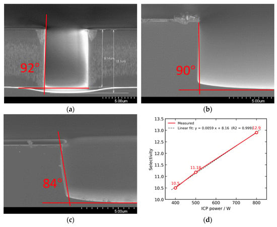
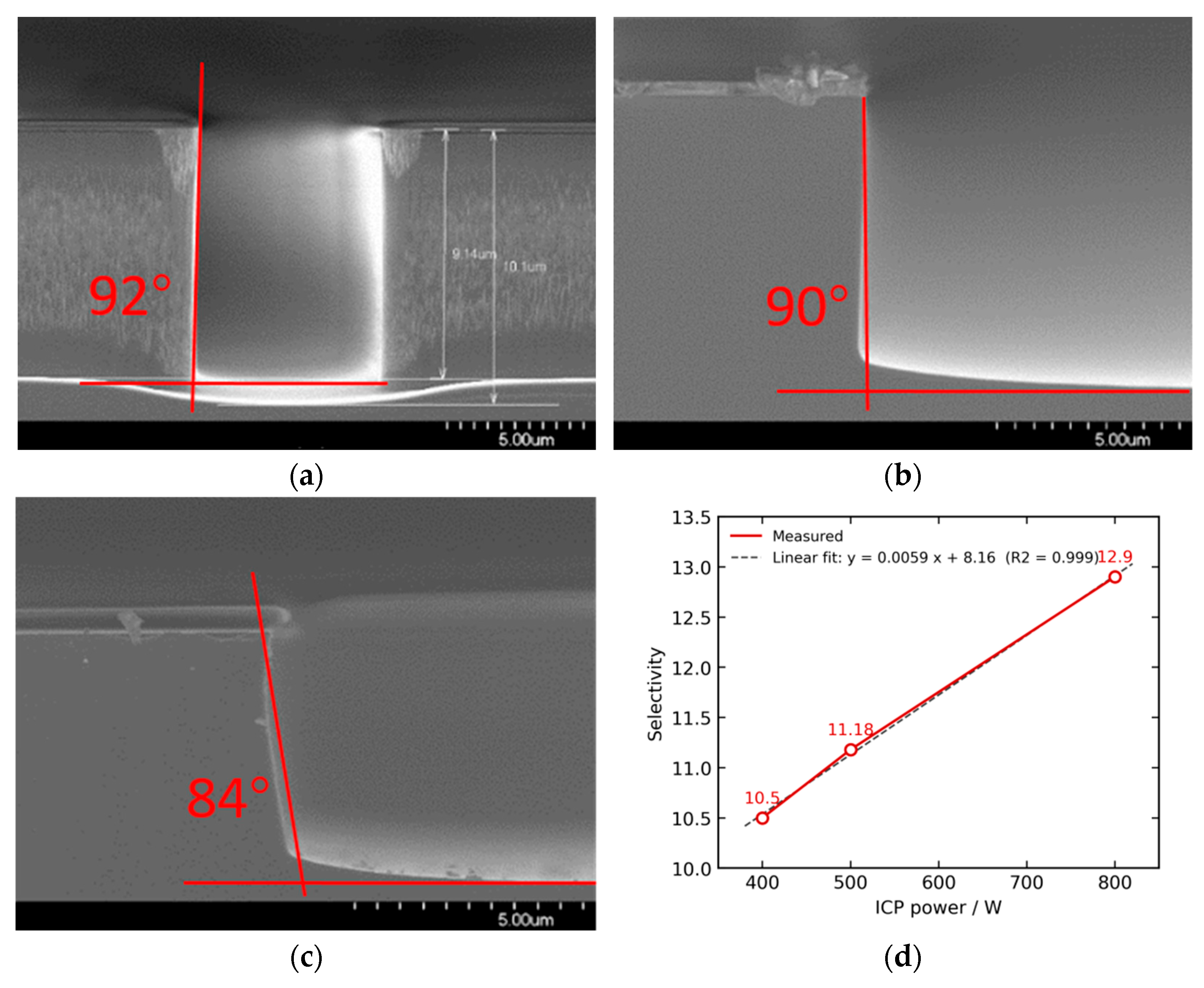
The ICP power mainly controls the plasma density. A higher ICP power increases the concentration of reactive species in the plasma and raises the etching rate. Figure 1 shows Experiments 1, 2 and 4, which were carried out in the Cl2/CH4/H2 mixture. When the ICP power was reduced from 800 to 400 W, the etching rate dropped from 16.8 to 8.3 nm/s. The selectivity fell at the same time, from 12.9 to 11.2 and 10.5, almost linearly with the ICP power. The linear fit in Figure 1d has a slope of 0.0059 per W and an R2 of 0.998. Over the same range the SiO2 etching rate, estimated from the etching rate and the selectivity, fell from about 1.3 to 0.8 nm/s. The InP etching rate fell more steeply, so the selectivity decreased. The sidewall angle, however, first improved from 92° to 90° and then degraded to 84° as the power was reduced further. A possible reason is that less of the deposited C–H polymer is removed at the lower power, so that a passivation layer builds up on the sidewalls and narrows the trench as it deepens, which would taper the profile.
Figure 1.
Cross-sectional scanning electron microscope (SEM) images of the sidewalls of InP etched in Cl2/CH4/H2 = 8/8/10 sccm at an RF power of 120 W and a chamber pressure of 4 mTorr. The ICP power was (a) 800 W, (b) 500 W and (c) 400 W (Experiments 1, 2 and 4). (d) Selectivity as a function of the ICP power, with a linear fit.
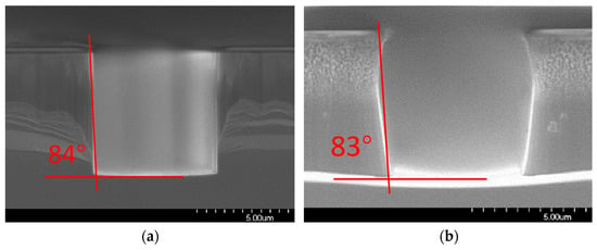
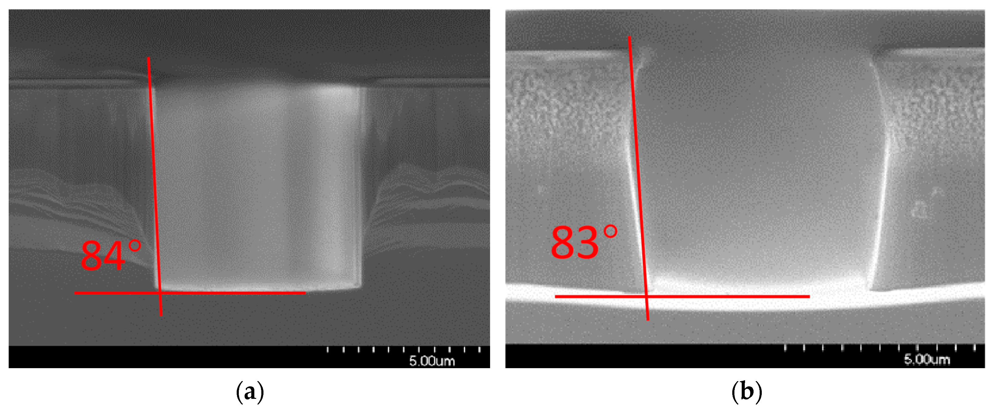
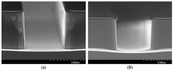
The RF power controls the ion bombardment energy. Experiments 8 and 9, shown in Figure 2, were run at RF powers of 50 and 150 W, but their gas flows also differ, as listed in Table 1. Experiment 9 etched faster than Experiment 8, at 11.1 nm/s compared with 7.8 nm/s. It also showed rough footing at the bottom of the trench, a sidewall angle of 84° and a lower selectivity of 7.6, compared with 8.4 for Experiment 8. This is consistent with stronger bombardment, although the contribution of the RF power cannot be isolated. Experiment 8 showed more lateral etching and a less vertical sidewall, with an angle of 83°. This is consistent with a dominant chemical component at low RF power, although its higher CH4 flow may also have contributed.
Figure 2.
SEM images of the sidewall and the trench bottom of the etched step. The ICP power was 800 W and the chamber pressure 4 mTorr. The RF power was (a) increased to 150 W (Experiment 9) and (b) reduced to 50 W (Experiment 8). The gas flows also differ between the two runs (Table 1).
2.2. Gas Composition and Flow Rate
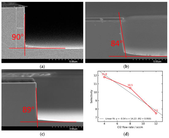
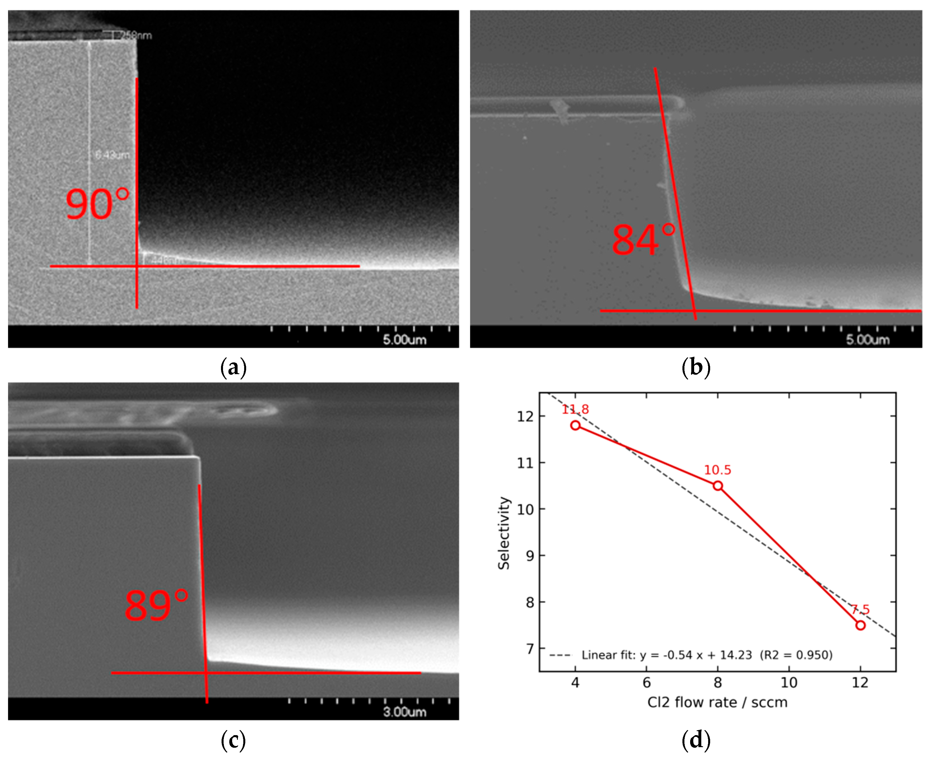
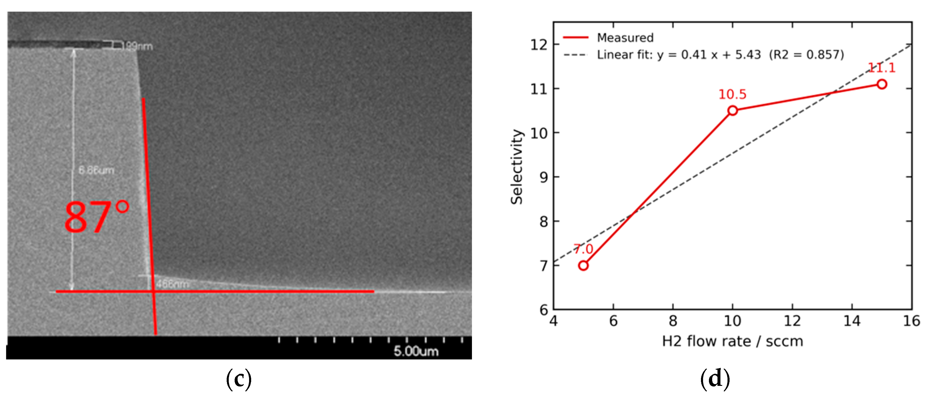
Figure 3, Figure 4, Figure 5 and Figure 6 show how the flow of each gas affects the etched profile and the selectivity. In each series one flow was stepped while the power, the pressure and the temperature were held constant. Figure 3d, Figure 4d and Figure 5d plots the selectivity against that flow with a linear fit, which describes the trend within the tested range only. Figure 6d compares two Ar flows. Cl2 is the main etchant gas and supplies the chlorine radicals (Cl·) for the chemical reaction. Figure 3 shows the Cl2 series, Experiments 3, 4 and 5, in which the Cl2 flow was raised from 4 to 8 and then 12 sccm at CH4/H2 = 8/10 sccm. The etching rate fell from 9.6 to 8.3 and then 6.3 nm/s, and the selectivity fell almost linearly, from 11.8 to 10.5 and 7.5. The linear fit in Figure 3d has a slope of −0.54 per sccm and an R2 of 0.95. The estimated SiO2 etching rate stayed at about 0.8 nm/s. Because the mask is removed mainly by ion sputtering, this suggests that the ion flux changed little and that the lower InP etching rate has a surface-chemical cause. At 30 °C the InClx formed on the surface has a low volatility and is removed mainly with ion assistance, as discussed in Section 2.3. A larger chlorine supply therefore builds up an InClx-rich layer on the surface, which further slows the reaction. A higher Cl2 flow also lowers the fractions of CH4 and H2 in the feed gas, from 36% to 27% for CH4 and from 45% to 33% for H2. These two gases supply the radicals that form volatile products such as In(CH3)x and PH3 [17,20]. This InClx layer was not detected in the EDX analysis described in Section 2.5, because the layer is thin compared with the probing depth of EDX, and because InClx reacts with moisture in air and releases volatile HCl, so little chlorine remains on the sidewall. X-ray photoelectron spectroscopy, which is surface-sensitive, has shown In–Cl bonds as the predominant byproduct on InP etched in a Cl2/Ar plasma [22]. The sidewall angle was 90° at 4 sccm, 84° at 8 sccm and 89° at 12 sccm. As Figure 3a shows, a foot about 450 nm high remained at the base of the sidewall at 4 sccm. At 8 sccm the sidewall tapered and residue was left on the trench bottom, as shown in Figure 3b. The lowest Cl2 flow therefore gave the highest rate and selectivity of this series.
Figure 3.
Cross-sectional SEM images of InP etched with Cl2 flows of (a) 4, (b) 8 and (c) 12 sccm (Experiments 3, 4 and 5; CH4/H2 = 8/10 sccm, RF/ICP = 120/400 W, 4 mTorr, 30 °C). Panel (b) is the same run as Figure 1c. (d) Selectivity as a function of the Cl2 flow, with a linear fit.
Figure 4.
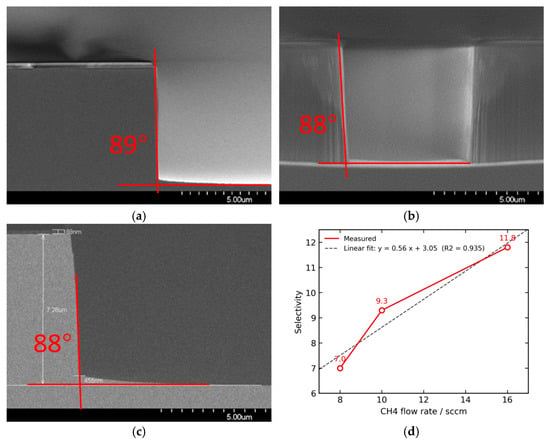
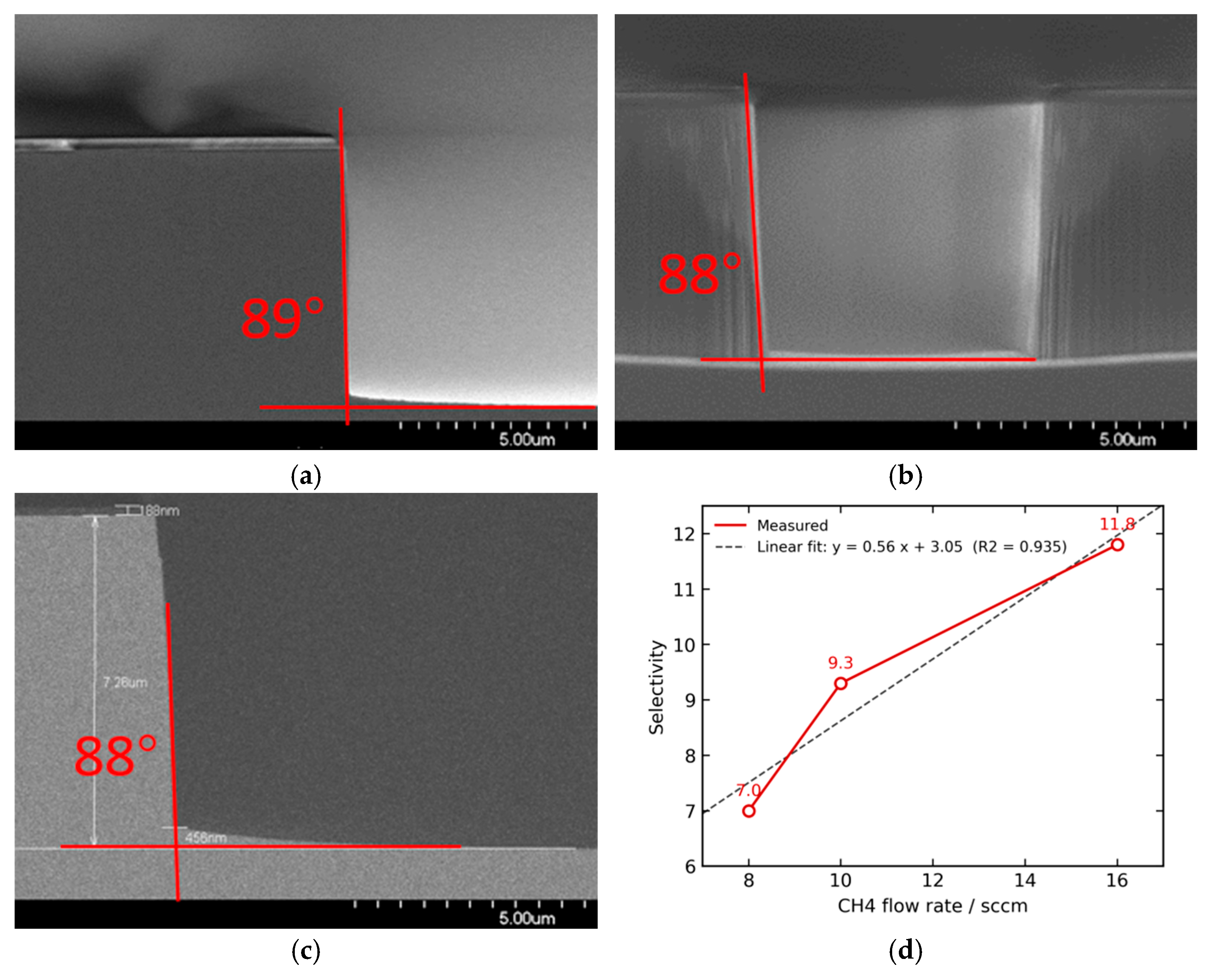
Cross-sectional SEM images of InP etched with CH4 flows of (a) 8, (b) 10 and (c) 16 sccm (Experiments 6, 10 and 11; Cl2/H2 = 8/5 sccm, RF/ICP = 120/400 W, 4 mTorr, 30 °C). (d) Selectivity as a function of the CH4 flow, with a linear fit.
Figure 6.
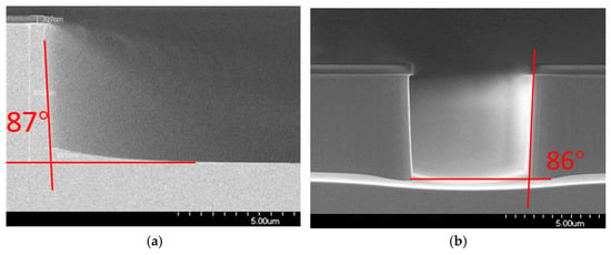
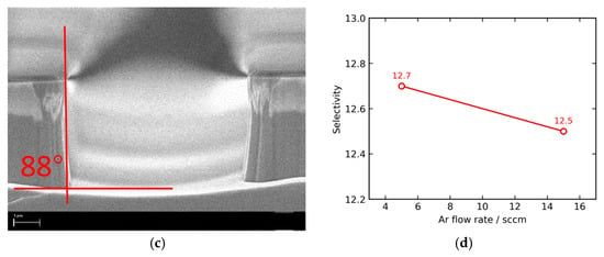
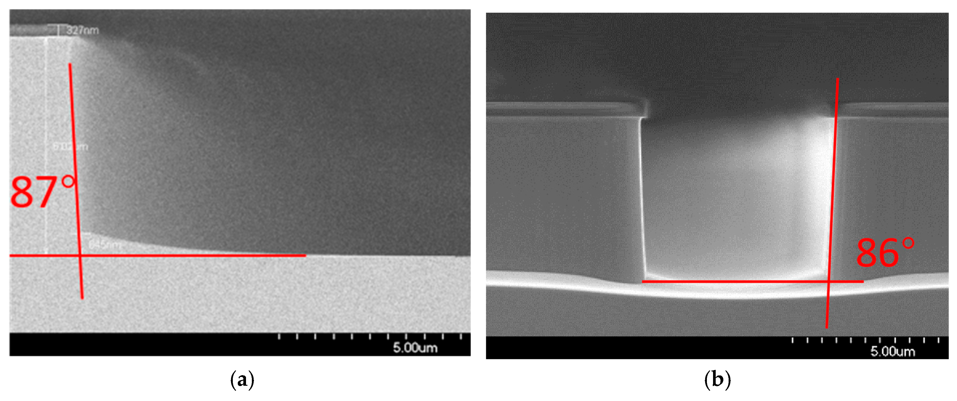
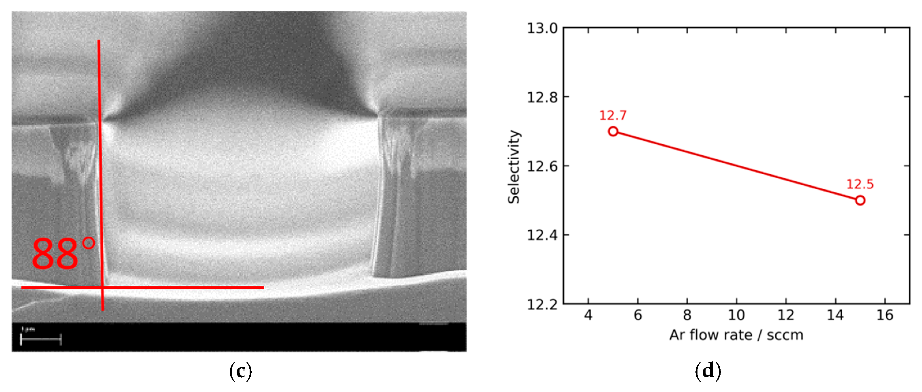
Cross-sectional SEM images of InP etched in the Cl2/Ar mixture (RF/ICP = 80/400 W, lower-electrode temperature setting 180 °C, 1 mTorr). (a) Cl2/Ar = 5/5 sccm (Experiment 16). (b) Cl2/Ar = 5/15 sccm (Experiment 15). (c) Cl2/Ar = 5/15 sccm with 2.5 sccm of CH4 added (Experiment 18). (d) Selectivity at Ar flows of 5 and 15 sccm.
CH4 is usually regarded as the sidewall passivating gas in this mixture. It is partly dissociated in the plasma, and the hydrocarbon species can deposit on the etched surfaces as a protective polymer layer that suppresses lateral etching. Whether such a polymer forms depends on the process conditions. Lee et al. observed no polymer formation in a Cl2/CH4/H2 process at an ICP power of 1200 W, which they attributed to cleaning by chlorine, and noted that more polymer could form at a higher pressure [17]. At the ICP power of 400 W used here, less of the deposit is expected to be removed. Si-containing sidewall passivation associated with the carrier wafer or reactor materials has also been reported for InP etching [19]. In the present experiments the Si carrier wafer and the eroded SiO2 mask could supply Si-containing species. Such deposits would, however, also be expected to act as micro-masks on the trench bottom and roughen it, and no grass-like features were observed on the trench bottoms in any of the experiments in Table 1. Hydrocarbon passivation is therefore regarded as the more likely mechanism here. Figure 4 shows the CH4 series, Experiments 6, 10 and 11, in which the CH4 flow was raised from 8 to 10 and then 16 sccm at Cl2/H2 = 8/5 sccm. Over this range the sidewall stayed close to vertical, at 89°, 88° and 88°. The selectivity rose steadily, from 7.0 to 9.3 and 11.8, and the linear fit in Figure 4d has a slope of 0.56 per sccm and an R2 of 0.94. The etching rate rose from 5.7 to 8.5 and 10.1 nm/s. The estimated SiO2 etching rate stayed between about 0.8 and 0.9 nm/s, so the higher selectivity came mainly from the faster InP etch. The profiles differed mainly at the base of the sidewall. Figure 4b shows that at 10 sccm the trench bottom was flat up to the sidewall, whereas Figure 4c shows a foot about 456 nm high at 16 sccm.
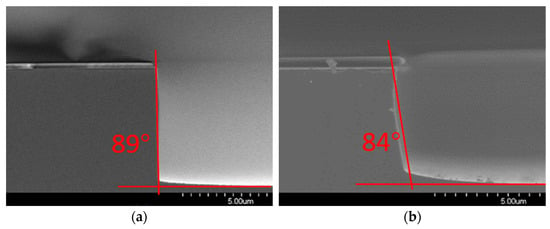
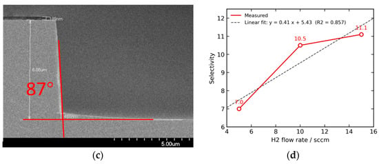
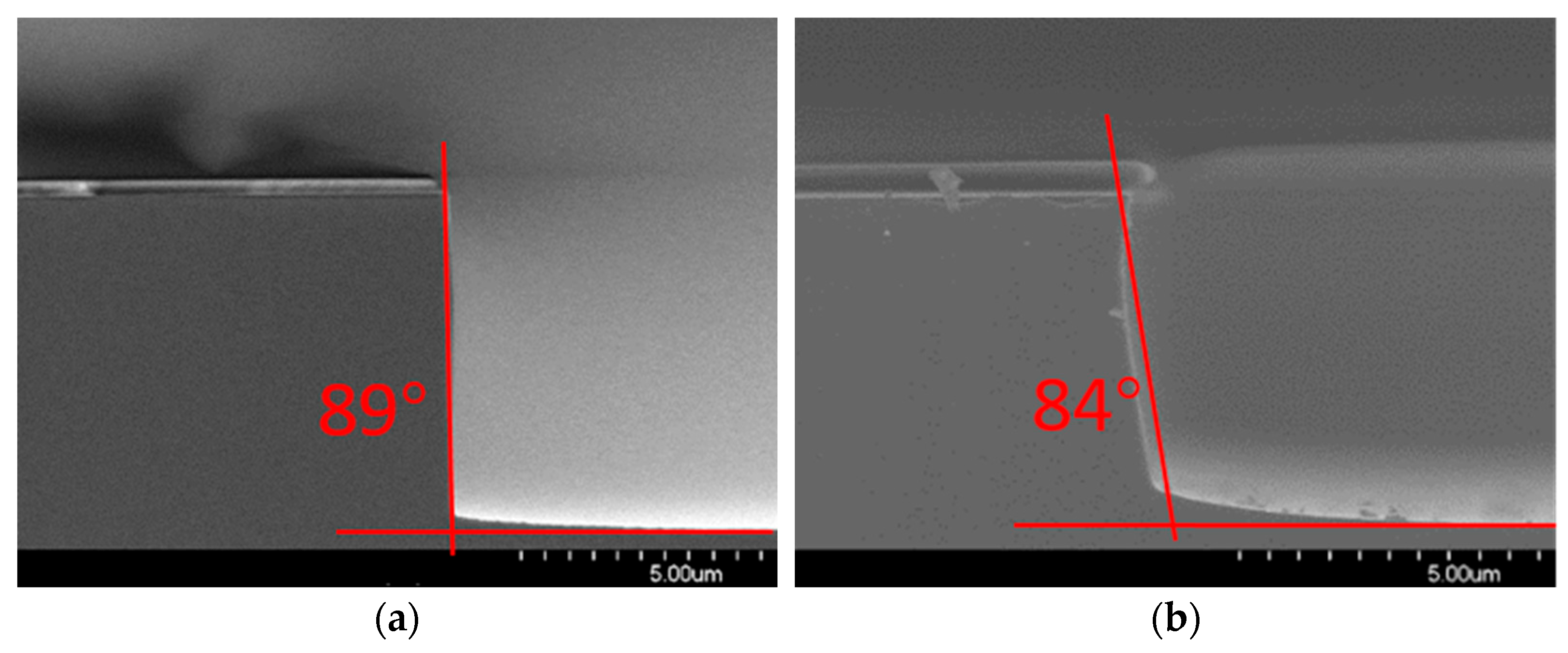
H2 takes part in the chemical reactions and regulates the concentration of hydrogen radicals in the plasma. Together with CH4, it is also thought to promote the formation of the carbon-based polymer and, thus, the passivation. Figure 5 shows the H2 series, Experiments 6, 4 and 7, in which the H2 flow was raised from 5 to 10 and then 15 sccm at Cl2/CH4 = 8/8 sccm. The selectivity rose from 7.0 to 10.5 and 11.1, most strongly between 5 and 10 sccm. The linear fit in Figure 5d has a slope of 0.41 per sccm and an R2 of 0.86. The etching rate rose from 5.7 to 8.3 and 9.3 nm/s. The sidewall angle did not follow the same trend. At 5 sccm the angle was 89°, and Figure 5a shows a vertical sidewall with a flat, clean bottom. At 10 sccm it fell to 84°, and in Figure 5b the sidewall tapered and residue remained on the trench bottom. At 15 sccm it recovered to 87°, and Figure 5c shows a foot about 466 nm high at the base. In all three series the SiO2 etching rate changed little, so the selectivity followed mainly the InP etching rate.
Ar is an inert gas and contributes to the physical etching in the Cl2/Ar mixture, together with chlorine-containing ions. Figure 6 shows the Ar series, in which the Cl2 flow was kept at 5 sccm and the Ar flow was raised from 5 sccm in Experiment 16 to 15 sccm in Experiment 15. The etching rate increased from 8.3 to 11.8 nm/s, the sidewall angle changed only from 87° to 86°, and the foot at the base of the sidewall became smaller, as Figure 6a,b shows. Figure 6d shows that the selectivity hardly changed, from 12.7 to 12.5. This is consistent with stronger ion-assisted removal, which accelerated the etching of InP and the erosion of the mask in about the same proportion. However, at a fixed Cl2 flow and pressure, raising the Ar flow also lowered the Cl2 fraction in the feed gas from 50% to 25%, which can change the dissociation, the ion composition, the ion flux and the self-bias. The higher etching rate therefore cannot be attributed to Ar+ bombardment alone. Only two Ar flows were tested, and the difference in selectivity is smaller than the run-to-run variation in less than 5% observed for the repeated runs in Section 3. The data therefore show only that the selectivity did not change significantly between these two flows. Experiment 15 was taken as the baseline for the Cl2/Ar mixture. Its sidewall angle was 86°, but the sidewall surface was slightly uneven. In Experiment 18, shown in Figure 6c, 2.5 sccm of CH4 was added to improve it. The etching rate dropped sharply to 3.7 nm/s, the selectivity fell to 5.3, and footing and increased lateral etching appeared. Under these conditions, adding CH4 did not improve the profile. Several factors may have contributed, including the lack of an effective carbon-based protective layer, the consumption of reactive chlorine by CH4-derived species, deposits at the trench bottom, a change in the plasma composition and nonuniform protection of the sidewall. The SEM images alone cannot distinguish between these possibilities.
2.3. Temperature
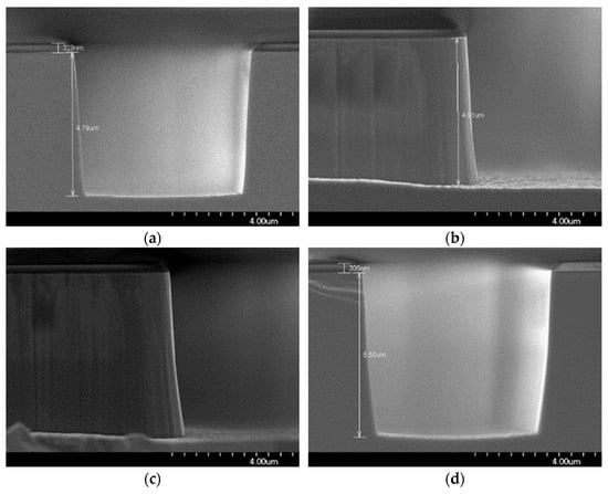
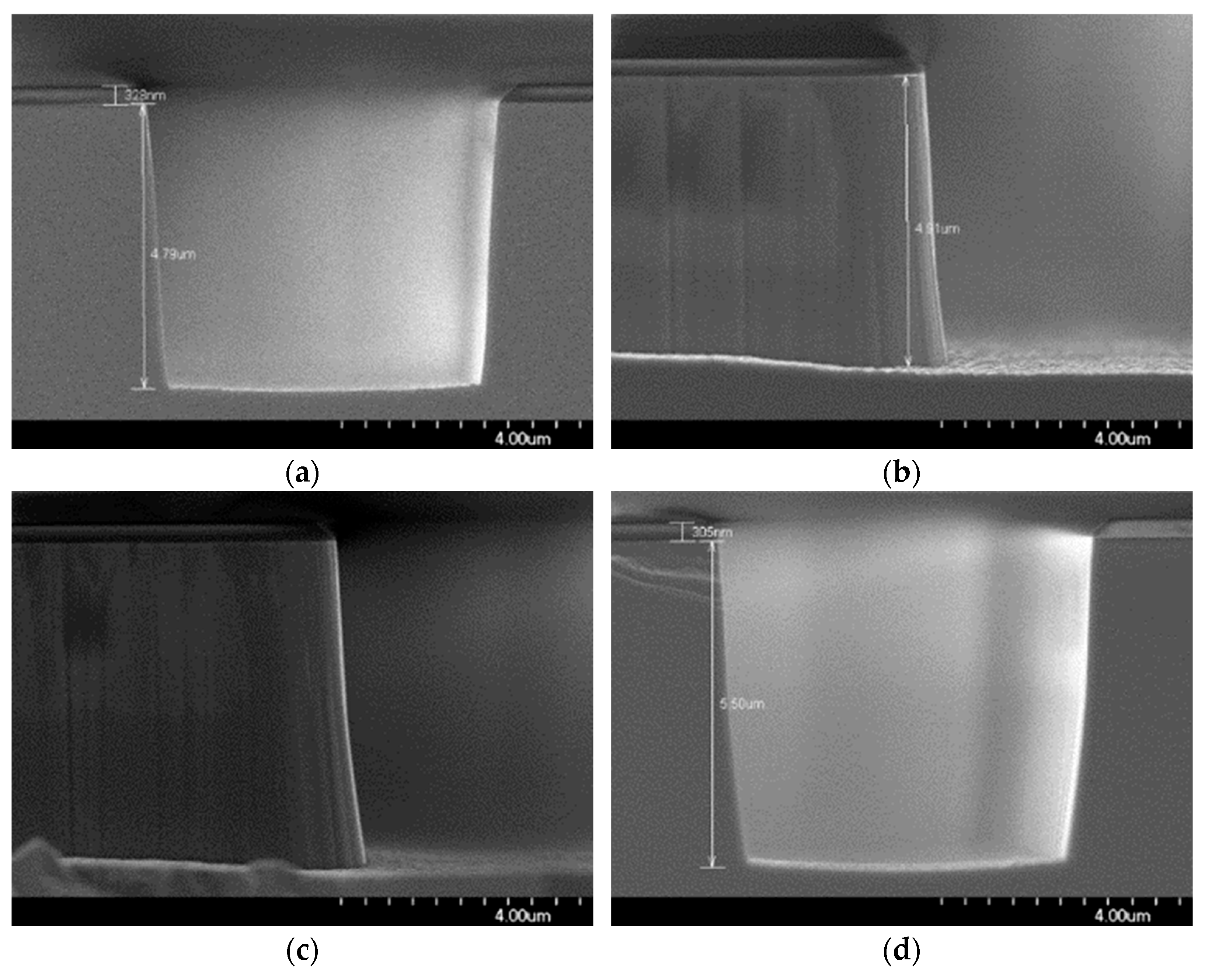
The temperature mainly affects the rate of the surface reactions and the desorption of the volatile by-products. In Cl2-based plasmas the InClx reaction products have a low volatility at room temperature [22]. If they are not desorbed efficiently, they accumulate on the surface. Where they mask the surface locally, the etching becomes nonuniform, an effect known as micro-masking. For this reason the substrate is usually heated to 150–200 °C in such processes [7,27]. Figure 7 shows the temperature series in the Cl2/CH4/H2 mixture, Experiments 6 and 12–14. The etching rate was 5.7 nm/s at both 30 and 180 °C and rose only to 6.2 and 6.5 nm/s at 230 and 270 °C. The selectivity was 7.0 at 30 and 180 °C and 7.8 at 230 and 270 °C, and the sidewall angle stayed at 88–89°. In the SEM images the sidewall surface appeared less rough at 230 °C, but it was still not completely smooth. Heating therefore brings only a modest gain in this mixture. The Cl2/Ar mixture behaved differently, as shown in Figure 8. When the temperature was raised from 180 °C in Experiment 15 to 230 °C in Experiment 17, the sidewall angle stayed at 86°, but the cross-sections differ clearly. At 180 °C the sidewall ran straight from the mask edge to the trench bottom, as shown in Figure 8a. At 230 °C both sidewalls bowed outward, so the trench was wider at mid-depth than at the mask opening, and the bottom corners were rounded, as shown in Figure 8b. The bowing indicates more lateral etching at the higher temperature. Without a passivating gas, the sidewalls are protected mainly because they receive few ions and the InClx formed on them is removed slowly. At 230 °C, faster thermal desorption allows neutral chlorine to etch the sidewalls with little ion assistance. Ions scattered at the mask edge probably strike the sidewall below the mask and enhance this lateral etching at mid-depth. The average etching rate, however, decreased from 11.8 to 7.7 nm/s. Bae et al. observed that the etching rate of InP in a Cl2/N2 plasma saturated near 200 °C, and attributed the saturation or decrease in the etching rate at high temperatures to the desorption of chlorine species before they react [22]. A similar effect may explain the lower rate at 230 °C here, and part of the chlorine may also be consumed by the sidewall etching. These explanations were not verified by surface or plasma diagnostics.
Figure 7.
Cross-sectional SEM images of the sidewalls etched in Cl2/CH4/H2 = 8/8/5 sccm at a chamber pressure of 4 mTorr. The temperatures were (a) 30, (b) 180, (c) 230 and (d) 270 °C (Experiments 6, 12, 13 and 14).
Figure 8.
Cross-sectional SEM images of the sidewalls etched in Cl2/Ar = 5/15 sccm at a chamber pressure of 1 mTorr. The temperature was (a) 180 and (b) 230 °C (Experiments 15 and 17).
In Experiment 19, shown in Figure 9, the RF power was raised to 120 W and the temperature lowered to 150 °C. The etching rate was 7.9 nm/s, but the mask receded. The two layers at the top of the ridges in Figure 9 are not two masks but a step in the InP left by this recession. As the mask edge retreated, the InP below it was exposed and etched back. The upper sidewall, exposed only after the recession, is rougher than the lower part because it was etched under a degraded mask edge. The EDX analysis of this sidewall is given in Section 2.5. The estimated SiO2 etching rate was 1.1 nm/s, compared with 0.9 nm/s in Experiment 15, which is consistent with stronger mask sputtering at the higher RF power. In both mixtures, a good compromise between rate, sidewall angle, morphology and mask protection is therefore best approached by adjusting the power, the gas ratio and the temperature together.
Figure 9.
SEM images of the sidewall etched in Cl2/Ar = 5/15 sccm after the lower-electrode temperature setting was lowered to 150 °C and the RF power raised to 120 W (Experiment 19).
2.4. EDX Analysis of the Sidewall
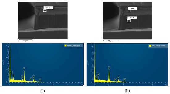
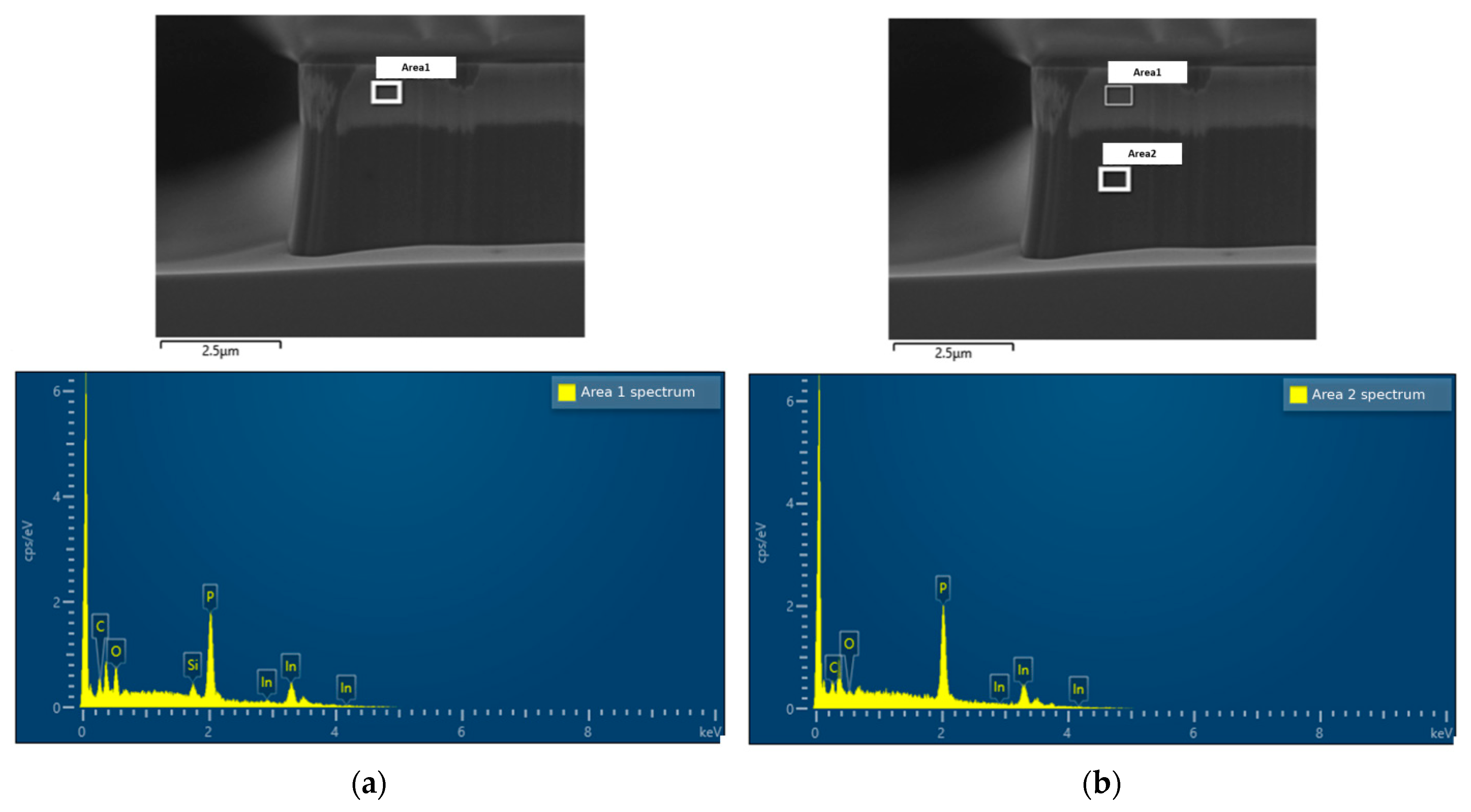
EDX was measured on the sidewall of Experiment 19. Figure 10 shows the two analyzed areas and their spectra, and Table 2 lists the composition. Area 1 lay in the rougher upper band, about 0.6 μm below the top edge, and area 2 on the smoother lower sidewall, about 2.4 μm below the top edge. Area 1 contained 1.57 wt% O and 0.93 wt% Si, which were not detected in area 2. These elements are attributed to the SiO2 mask, and their presence in area 1 only is consistent with the upper band being exposed after the mask receded, as described in Section 2.3. Area 1 also contained slightly more carbon than area 2, 0.76 ± 0.11 wt% compared with 0.49 ± 0.10 wt%. Since no carbon-containing gas was used in Experiment 19, this carbon may come from deposits left on the chamber walls by the Cl2/CH4/H2 runs or from surface contamination, and the difference is close to the measurement uncertainty. In and P are the signal of the InP substrate, and no chlorine was detected, as discussed in Section 2.2. Even at 5 kV, EDX probes a depth of a few hundred nanometers, so it cannot resolve a passivation film that is only nanometers to tens of nanometers thick. Confirming the mechanisms proposed in this section would require X-ray photoelectron spectroscopy and optical emission spectroscopy.
Figure 10.
SEM images and energy-dispersive X-ray (EDX) spectra of a sidewall from Experiment 19. (a) Area 1 in the upper band and its spectrum. (b) Areas 1 and 2, with the spectrum of area 2.
Table 2.
EDX composition (wt%) of the two sidewall areas of Experiment 19 (Figure 10). The uncertainties are the 1σ values given by the analysis software. n.d., not detected.
2.5. Comparison of the Two Routes
The two routes reach the same target profile through different mechanisms, as summarized in Table 3. In the Cl2/CH4/H2 mixture, the sidewall is thought to be protected by a hydrocarbon film deposited from CH4 and H2 while the bottom continues to be cleared, so the process can be run at 30 °C. The Cl2/Ar mixture contains no passivating gas. It combines chlorine-based chemical etching with directional ion bombardment and with heating, which assists the desorption of InClx. The Cl2/CH4/H2 route offers an additional degree of freedom in the CH4:H2 ratio, but at the selected conditions its etching rate and selectivity were lower. Experiment 10 gave an etching rate of 8.5 nm/s and a selectivity of 9.3, whereas Experiment 15 gave 11.8 nm/s and 12.5. Because each process was optimized within its own chemistry, the two also differ in RF power, pressure and temperature, so this is a comparison of two complete processes rather than an isolated test of the gas chemistry.
Table 3.
Comparison of the two chlorine-based routes.
3. Final Process Conditions
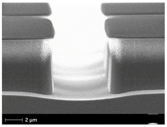
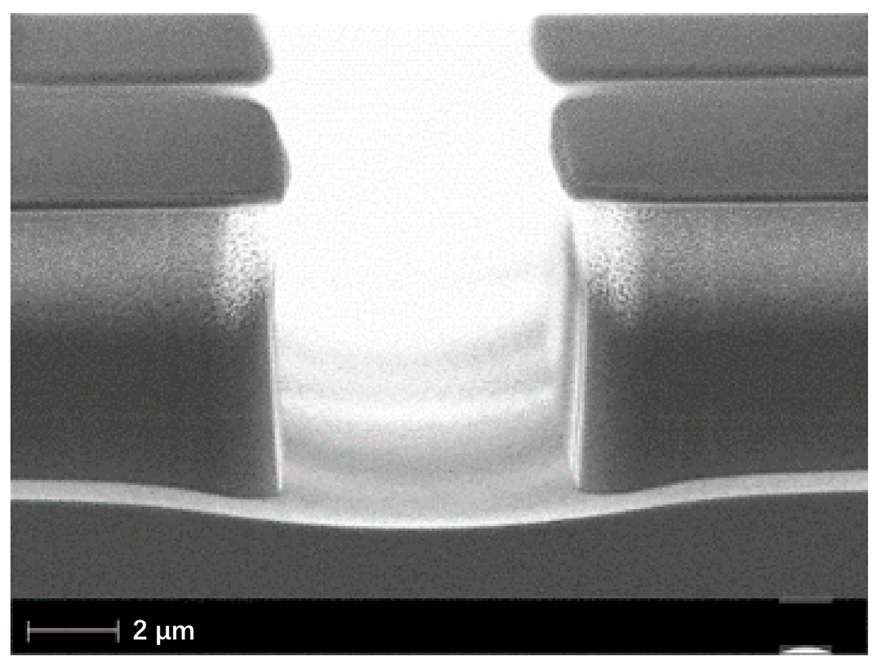
Based on these results, Experiment 10 was chosen for the Cl2/CH4/H2 mixture, with the ICP power kept low at 400 W, the CH4 flow adjusted to 10 sccm and the H2 flow kept at 5 sccm. Its profile is shown in Figure 4b. The etching rate was 8.5 nm/s and the sidewall angle 88°. The trench bottom was smooth and the mask did not recede. Experiments 3 and 11 gave a higher selectivity, but both left a foot about 450 nm high at the base of the sidewall, as seen in Figure 3a and Figure 4c, whereas the trench bottom in Experiment 10 was flat up to the sidewall. Experiment 10 therefore gives the best balance between rate, morphology and selectivity for this mixture.
The Cl2/Ar mixture was etched at an elevated temperature, and the baseline condition of Experiment 15, shown in Figure 6b, was retained. It used an RF power of 80 W, an ICP power of 400 W, Cl2/Ar flow rates of 5/15 sccm and a lower-electrode temperature setting of 180 °C. The sidewall angle was 86° and the selectivity 12.5. The trench bottom was smooth, and the overall profile met the requirements.
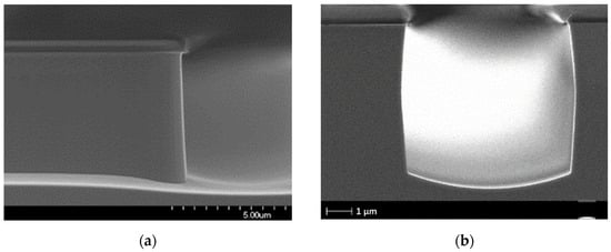
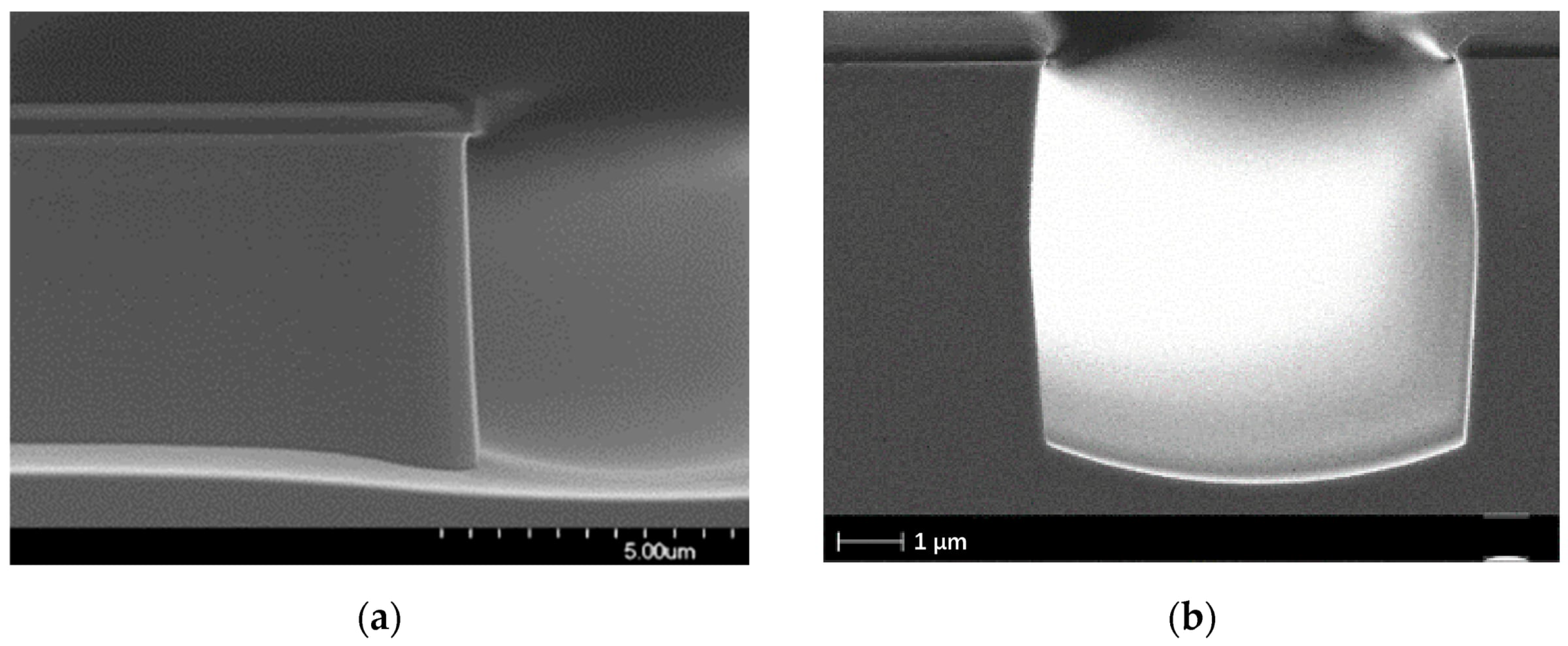
Both selected processes were repeated under the same conditions, and Figure 11 shows the sidewalls from these repeated runs. The repeated profiles agreed with those of the first runs in Figure 4b and Figure 6b, and the etching rate and the selectivity differed by less than 5%.
Figure 11.
Repeated runs of the two selected processes: (a) Cl2/CH4/H2 under the conditions of Experiment 10 and (b) Cl2/Ar under the conditions of Experiment 15.
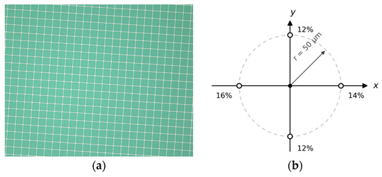
The trenches were applied to a 128 × 128 SPAD array with a pixel pitch of 50 μm, in which they were etched through all epitaxial layers with the Cl2/Ar process of Experiment 15. Figure 12a shows an optical microscope (OM) image of part of the array. The pixels form a regular square grid and are separated by continuous trenches of uniform width. Lateral crosstalk was measured in photon-counting mode, with a single pixel used as the aggressor. At 0 °C and a photon detection efficiency (PDE) of 8%, the crosstalk probability at the four nearest-neighbor pixels was 12–16%, as shown in Figure 12b. The crosstalk probability increases with the PDE, because more carriers take part in crosstalk, and it also increases with temperature. Because of the avalanche gain of SPADs, isolation trenches are essential to suppress the electrical and direct optical crosstalk between adjacent pixels. The ICP parameters mainly determine the shape and roughness of the trenches, and in our current results the trench shape had little effect on the crosstalk, the PDE and the dark count rate. The remaining crosstalk can be reduced further by adding an absorbing metal between the rear micro-lenses.
Figure 12.
(a) Optical microscope (OM) image of part of the 128 × 128 single-photon avalanche diode (SPAD) array (pixel pitch 50 μm). (b) Crosstalk probability at the four nearest-neighbor pixels of a single aggressor pixel (0 °C, photon detection efficiency 8%).
4. Conclusions
Deep-trench structures are needed in InP-based chips, and the ICP etching of such structures was studied experimentally in this work. The effects of key process parameters on the etched morphology and the underlying mechanisms were examined for the Cl2/CH4/H2 and Cl2/Ar gas mixtures, and optimized conditions were obtained for each. Under the optimized conditions both processes etched trenches about 6 μm deep. In cross-sectional SEM images the sidewalls appeared vertical and smooth, and the bottoms flat. In a 128 × 128 SPAD array with a pixel pitch of 50 μm, isolated with the Cl2/Ar process, the crosstalk probability at the four nearest-neighbor pixels was 12–16% at 0 °C and a photon detection efficiency of 8%. These results confirmed the feasibility of both processes for morphology control. Because the two routes rely on different mechanisms, the comparison between them provides a direct basis for choosing between a room-temperature process with polymer-forming gases and a heated process without them.
Author Contributions
Conceptualization, L.Z. (Lichen Zhang); Methodology, L.Z. (Lichen Zhang); Validation, L.L.; Formal analysis, L.Z. (Lichen Zhang), L.L., W.Z., S.T., L.Z. (Li Zhou), J.W. and Y.S.; Data curation, H.Z.; Writing—original draft, L.Z. (Lichen Zhang); Writing—review & editing, H.Z. and Y.S.; Supervision, J.W. and Y.S.; Project administration, J.W. and Y.S.; Funding acquisition, Y.S. All authors have read and agreed to the published version of the manuscript.
Funding
This work was supported by the Major Science and Technology Project of Yunnan Province (Grant No. 202402AC080001), and the National Natural Science Foundation of China (Grant No. 62665016).
Institutional Review Board Statement
Not applicable.
Informed Consent Statement
Not applicable.
Data Availability Statement
The original contributions presented in this study are included in the article. Further inquiries can be directed to the corresponding authors.
Conflicts of Interest
Authors Liujing Li, Wu Zhao, Shaoyang Tan, Li Zhou, Jun Wang were employed by the company Suzhou Everbright Photonics Co., Ltd. The remaining authors declare that the research was conducted in the absence of any commercial or financial relationships that could be construed as a potential conflict of interest.
References
- Chang, F.; Bhoja, S. New paradigm shift to PAM4 signalling at 100/400G for cloud data centers: A performance review. In Proceedings of the 2017 European Conference on Optical Communication (ECOC), Gothenburg, Sweden, 17–21 September 2017; IEEE: Piscataway, NJ, USA, 2017; pp. 1–3. [Google Scholar]
- Coldren, L.A.; Verrinder, P.A.; Klamkin, J. A review of photonic systems-on-chip enabled by widely tunable lasers. IEEE J. Quantum Electron. 2022, 58, 6300110. [Google Scholar] [CrossRef] [Scilit]
- Jiang, X.; Wilton, S.; Kudryashov, I.; Itzler, M.A.; Entwistle, M.; Kotelnikov, J.; Katsnelson, A.; Piccione, B.; Owens, M.; Slomkowski, K.; et al. InGaAsP/InP Geiger-mode APD-based LiDAR. In Proceedings of Optical Sensing, Imaging, and Photon Counting: From X-Rays to THz, San Diego, CA, USA, 22–23 August 2018; SPIE: Bellingham, WA, USA, 2018; Volume 10729, pp. 33–44. [Google Scholar]
- Gao, L.; Zhang, X.; Ma, J.; Yao, Q.; Wang, Q.; Sun, Y.; Liu, Z.; Wang, Y.; Tian, L.; Zheng, Y. Quantum enhanced Doppler LiDAR based on integrated quantum squeezed light source. Infrared Laser Eng. 2021, 50, 20210031. [Google Scholar]
- Khan, M.J.; Skelly, L.; Vasile, A.; Francis, T.; Drover, J.; Rivera, D.; Hatch, R.; Dumanis, D.; McIntosh, K.; Frechette, J.; et al. Remote sensing impact of single-photon sensitive airborne lidar systems based on Geiger-mode avalanche photodiode arrays. In Proceedings of the IGARSS 2024–2024 IEEE International Geoscience and Remote Sensing Symposium; IEEE: Piscataway, NJ, USA, 2024; pp. 2455–2459. [Google Scholar]
- Deng, L. Dry etching of InP-based materials using a high-density ICP plasma system. Semicond. Today Compd. Adv. Silicon 2012, 7, 82–87. [Google Scholar]
- Ishutkin, S.V.; Arykov, V.S.; Yunusov, I.V.; Stepanenko, M.V.; Troyan, P.E.; Zhidik, Y.S. Low temperature ICP etching of InP/InGaAsP heterostructure in Cl2-based plasma. J. Phys. Conf. Ser. 2019, 1393, 012088. [Google Scholar] [CrossRef] [Scilit]
- Kindt, W.J.; van Zeijl, H.W.; Middelhoek, S. Optical cross talk in Geiger mode avalanche photodiode arrays: Modeling, prevention and measurement. In Proceedings of the 28th European Solid-State Device Research Conference (ESSDERC); IEEE: Piscataway, NJ, USA, 1998; pp. 192–195. [Google Scholar]
- Verghese, S.; McIntosh, K.A.; Liau, Z.L.; Sataline, C.; Shelton, J.D.; Donnelly, J.P.; Funk, J.E.; Younger, R.D.; Mahoney, L.J.; Smith, G.M.; et al. Arrays of 128 × 32 InP-based Geiger-mode avalanche photodiodes. Proc. SPIE 2009, 7320, 73200M. [Google Scholar]
- Siwak, N.P.; Fan, X.Z.; Ghodssi, R. Fabrication challenges for indium phosphide microsystems. J. Micromech. Microeng. 2015, 25, 043001. [Google Scholar] [CrossRef] [Scilit]
- Docter, B.; Geluk, E.J.; Sander-Jochem, M.J.H.; Karouta, F.; Smit, M. Deep etched DBR gratings in InP for photonic integrated circuits. In Proceedings of the International Conference on Indium Phosphide and Related Materials (IPRM 2007), Matsue, Japan, 14–18 May 2007; IEEE: Piscataway, NJ, USA, 2007; pp. 226–228. [Google Scholar]
- Jiao, Y.; de Vries, T.; Unger, R.S.; Shen, L.; Ambrosius, H.; Radu, C.; Arens, M.; Smit, M.; van der Tol, J. Vertical and smooth single-step reactive ion etching process for InP membrane waveguides. J. Electrochem. Soc. 2015, 162, E90–E95. [Google Scholar] [CrossRef] [Scilit]
- Liu, C.; Wang, W.; Wang, Y.; Qu, H.; Zhou, M.; Chen, J.; Wu, T.; Lin, J.; Ou, M.; Li, C.; et al. Process Study and Optimization of ICP Etching Chemistries for Continuous Curved-Profile Transfer of InP Microlenses. Mater. Sci. Semicond. Process. 2026, 216, 111094. [Google Scholar] [CrossRef] [Scilit]
- Xie, R.; Shan, Y.; Yao, L.; Wu, D.; Su, X.; Hao, H.; Jiang, D.; Yang, M.; Zhang, Y.; Xie, H.; et al. An InGaAsSb Based 640 × 512 Focal Plane Array with Low Surface Leakage Current for Extended Shortwave Detection. IEEE Photonics J. 2025, 17, 6801206. [Google Scholar] [CrossRef] [Scilit]
- Chen, X.; Wang, X.; Sun, J.; Zhang, Y.; Gao, F.; Wang, Y. Global Model Studies of Species Composition and Chemical Reactions in Inductively Coupled HBr/Cl2/Ar Plasmas. Plasma Sci. Technol. 2025, 27, 125401. [Google Scholar] [CrossRef] [Scilit]
- Aksakal, R.; Cakmak, B. ICP-RIE etching of InP using CH4/H2, CH4/H2/Cl2, H2/Cl2 and Cl2: Process development and optimization. Laser Phys. 2025, 35, 065002. [Google Scholar] [CrossRef] [Scilit]
- Lee, C.W.; Nie, D.; Mei, T.; Chin, M. Study and optimization of room temperature inductively coupled plasma etching of InP using Cl2/CH4/H2 and CH4/H2. J. Cryst. Growth 2006, 288, 213–216. [Google Scholar] [CrossRef] [Scilit]
- Wieczorek, A.; Djara, V.; Peters, F.H.; O’cAllaghan, J.; Thomas, K.; Corbett, B. Inductively coupled plasma deep etching of InP/InGaAsP in Cl2/CH4/H2 based chemistries with the electrode at 20 °C. J. Vac. Sci. Technol. B 2012, 30, 051208. [Google Scholar] [CrossRef] [Scilit]
- Gatilova, L.; Bouchoule, S.; Guilet, S.; Chabert, P. Investigation of InP etching mechanisms in a Cl2/H2 inductively coupled plasma by optical emission spectroscopy. J. Vac. Sci. Technol. A 2009, 27, 262–275. [Google Scholar] [CrossRef] [Scilit]
- Yu, J.S.; Lee, Y.T. Parametric reactive ion etching of InP using Cl2 and CH4 gases: Effects of H2 and Ar addition. Semicond. Sci. Technol. 2002, 17, 230–236. [Google Scholar]
- Efremov, A.M.; Kim, D.P.; Kim, C.I. Inductively coupled Cl2/Ar plasma: Experimental investigation and modeling. J. Vac. Sci. Technol. A 2003, 21, 1568–1573. [Google Scholar] [CrossRef] [Scilit]
- Bae, J.W.; Jeong, C.H.; Lim, J.T.; Lee, H.C.; Yeom, G.Y.; Adesida, I. Anisotropic etching of InP and InGaAs by using an inductively coupled plasma in Cl2/N2 and Cl2/Ar mixtures at low bias power. J. Korean Phys. Soc. 2007, 50, 1130–1135. [Google Scholar] [CrossRef] [Scilit]
- Yoon, S.F.; Ng, T.K.; Zheng, H.Q. Study of GaAs and GaInP etching in Cl2/Ar electron cyclotron resonance plasma. Thin Solid Films 2001, 394, 249–254. [Google Scholar] [CrossRef] [Scilit]
- Rhallabi, A.; Chanson, R.; Landesman, J.P.; Cardinaud, C.; Fernandez, M.-C. Atomic scale study of InP etching by Cl2-Ar ICP plasma discharge. Eur. Phys. J. Appl. Phys. 2011, 53, 33606. [Google Scholar] [CrossRef] [Scilit]
- Rawal, D.S.; Arora, H.; Agarwal, V.R.; Vinayak, S.; Kapoor, A.; Sehgal, B.; Muralidharan, R.; Saha, D.; Malik, H. GaN etch rate and surface roughness evolution in Cl2/Ar based inductively coupled plasma etching. Thin Solid Films 2012, 520, 7212–7218. [Google Scholar] [CrossRef] [Scilit]
- Lee, J.W.; Hong, J.; Abernathy, C.R.; Lambers, E.S.; Pearton, S.J.; Hobson, W.S.; Ren, F. Cl2/Ar plasma etching of binary, ternary, and quaternary In-based compound semiconductors. J. Vac. Sci. Technol. B 1996, 14, 2567–2573. [Google Scholar] [CrossRef] [Scilit]
- Ishutkin, S.; Arykov, V.; Yunusov, I.; Stepanenko, M.; Smirnov, V.; Troyan, P.; Zhidik, Y. The method of low-temperature ICP etching of InP/InGaAsP heterostructures in Cl2-based plasma for integrated optics applications. Micromachines 2021, 12, 1535. [Google Scholar] [CrossRef] [Scilit] [PubMed]

Disclaimer/Publisher’s Note: The statements, opinions and data contained in all publications are solely those of the individual author(s) and contributor(s) and not of MDPI and/or the editor(s). MDPI and/or the editor(s) disclaim responsibility for any injury to people or property resulting from any ideas, methods, instructions or products referred to in the content. |
© 2026 by the authors. Licensee MDPI, Basel, Switzerland. This article is an open access article distributed under the terms and conditions of the Creative Commons Attribution (CC BY) license.