


Abstract
The global transition to renewable energy has made photovoltaics a potential primary energy source, due to the abundance of solar radiation worldwide and the technological maturity of conversion systems. In this context, cadmium telluride (CdTe) remains one of the leading thin-film absorber materials due to its near-optimal bandgap (~1.5 eV) and high absorption coefficient; however, conventional CdTe-based devices face three factors that limit their efficiency: parasitic absorption in the standard cadmium sulfide (CdS) window layer, non-radiative recombination at the interfaces, and the economically costly requirement for thick absorber layers (3 to 5 µm) given the high cost of CdTe. This work proposes a dual-interface passivation strategy that simultaneously addresses loss mechanisms at both the front and back surfaces. At the front interface, the conventional CdS buffer layer is replaced by a Cd(1−x)Zn(x)S alloy, whose tunable bandgap (2.4–3.7 eV) suppresses parasitic absorption in the ultraviolet and blue regions and improves band alignment with CdTe, thereby increasing the short-circuit current and open-circuit voltage. At the rear interface, a CuInTe2 (CIT) rear surface field layer is introduced between the CdTe absorber and the molybdenum (Mo) rear contact to counteract the Schottky barrier responsible for degrading hole collection. These two modifications, when implemented together, yield efficiency gains greater than those previously reported in the literature, while also enabling a substantial reduction in the thickness of the CdTe absorber to 1 µm. Using one-dimensional drift-diffusion simulations (wxAMPS) under standard AM 1.5G illumination, this study systematically evaluates the influence of the zinc content in the Cd(1−x)Zn(x)S buffer layer and the thickness of the CuInTe2 layer on the key photovoltaic performance metrics (Jsc, Voc, FF, and efficiency), with the aim of identifying the optimal device configuration for high-performance and cost-effective CdTe thin-film solar cells.
1. Introduction
In the context of the global energy transition driven by climate change, photovoltaic energy has emerged as one of the most promising solutions [1,2]. This energy source is no longer considered only as a secondary solution for specific applications, such as off-grid sites [3] or charging systems [4], but as a potentially primary energy source capable of contributing to the stabilization of the electrical grid [5]. This choice is justified by the worldwide abundance of solar radiation [6] and the technological maturity of conversion systems [7]. In this context, research efforts have focused on improving efficiency, most notably through power maximization techniques such as Maximum Power Point Tracking [8], or the use of intelligent approaches for fault detection and performance optimization [9]. Among these research directions, optimizing photovoltaic cell performance during manufacturing constitutes a key approach [10].
Optimization of photovoltaic cell performance at the manufacturing stage depends on multiple factors such as the selection and quality of semiconductor materials, the arrangement of the absorber and buffer layers, and the electrical contacts to improve light absorption and lower recombination of lost carriers [11]. Using buffer layers or Back Surface Field (BSF) layers reduces interfacial recombination and more efficient charge harvesting. On top of that, using novel alloys or semiconductors for the same materials leads to bandgap extension, less parasitic absorption, and better thermal and chemical stability. Altogether, these methods raise the output power, decrease the use of expensive materials, make the photovoltaic system perform better, as well as be more cost-effective.
Cadmium telluride (CdTe) is considered among the thin-film technologies as an outstanding option for the production of high-performance solar cells [12]. The physical properties of CdTe are very favorable, such as a bandgap that almost matches the optimum for solar (~1.5 eV), extremely high optical absorption ability, and good electron mobility, which make it possible to achieve complete light absorption even with very thin absorber layers [12]. However, their efficiency is still constrained by several issues, e.g., parasitic absorption in the usual CdS window layer [13,14], non-radiative interfacial recombinations, and thicker absorbent layers which result in higher production costs [13].
In order to address these issues, numerous optimization methods have been investigated. One particularly interesting study examined the use of an MXene (Ti2C3) enriched buffer layer in SnO2 as a front-side passivation, resulting in an improvement in the fill factor from 82.87% to 84.82% and in efficiency from 21.86% to 22.42%. Other researchers have chosen to optimize the cells by incorporating Mg into the ZnO layer to increase the bandgap to 3.75 eV, thereby improving efficiency [15]. Further optimization studies have focused on passivating the back side of the cell by adding an additional layer between the absorber and the rear contact, such as a BSF, to create a field that repels carriers toward the space charge region. Research on the insertion of a ZnTe- and ZnTe:Cu-based BSF [16], as well as the use of perovskite such as CH3NH3SnBr3 [17], has resulted in significant optimization in terms of efficiency. The studies cited, as well as most previous studies, use standard CdTe thicknesses (3–5 µm), which represents a significant economic loss given the high cost of producing CdTe [18].
The approach of substituting Cadmium Sulphide (CdS) with Cadmium Zinc Sulphide Cd(1−x)Zn(x)S alloy allows bandgap expansion and reduces parasitic absorption, which leads to an increase in short-circuit current and Voc (open-circuit voltage). At the same time, the employment of a Back Surface Field (BSF) layer of Copper Indium Ditelluride (CuInTe2) improves the carrier collection from the rear contact and reduces recombination losses. This combined approach improves electrical performance while reducing the thickness of the CdTe layer to just 1 µm, which both reduces material consumption and maintains very high solar cell conversion efficiencies. Indeed, the integrated optimization of both the buffer and BSF layers therefore represents a rigorous and economically viable pathway toward high-performance CdTe solar cells capable of meeting the demands of modern photovoltaic systems.
In this work, we aimed to:
- -
- Perform front-side passivation by introducing Cd(1−x)Zn(x)S: The CdS is known as the conventional window layer, traditionally chosen for its good crystalline compatibility and ease of deposition with CdTe; however, it has a major limitation: its relatively narrow bandgap (~2.4 eV) absorbs a significant portion of blue and ultraviolet photons (λ < 500 nm) [13,14], which directly reduces the short-circuit current density (Jsc) compared to a theoretically transparent window layer [19]. When we replace the CdS with a Cd(1−x)Zn(x)S alloy in which the zinc fraction varies from 0 to 1, this substitution widens the bandgap, suppressing parasitic absorption in the 300–500 nm spectral range. Although the reduction in interfacial recombination is recognized as being beneficial for Voc in wide-bandgap buffer-layer heterojunctions [20], our simulations show that, for the structure studied here, which includes a CIT layer at the back contact, Voc remains limited by a mechanism distinct from that at the front interface such that the improvement resulting from the incorporation of Zn is primarily reflected in an increase in Jsc rather than in an increase in Voc [20].
- -
- Perform back-side passivation by introducing a CuInTe2 layer simultaneously with the front-side passivation: At the rear CdTe/Mo interface, the Schottky barrier arising from the electron affinity of CdTe (~4.3 eV) and the work function of molybdenum (~4.6 eV) impedes hole collection, reducing the fill factor by 5–10% and lowering the open-circuit voltage by 50–100 mV relative to theoretical predictions [21]. To overcome this limitation, a CuInTe2 (CIT) Back Surface Field layer is inserted between the CdTe absorber and the Mo rear contact. As a chalcopyrite semiconductor with a bandgap of ~1.0 eV and a crystal structure compatible with CdTe, CuInTe2 establishes a reverse electric field through the bandgap gradient at the rear interface, thereby reducing electron injection barriers, improving hole collection efficiency, and enhancing both the fill factor and the overall device voltage [22,23].
The combined integration of the Cd(1−x)Zn(x)S buffer layer and the CuInTe2 BSF layer addresses two distinct and complementary loss pathways simultaneously: Cd(1−x)Zn(x)S primarily mitigates photocurrent losses attributable to parasitic absorption at the front interface, while the CuInTe2 BSF layer targets rear-contact recombination, improving voltage and fill factor. The synergy between these two optimizations enables simultaneous enhancement of both photocurrent and voltage, yielding an overall cell efficiency that surpasses what either modification could achieve independently.
In addition to these electrical advantages, the proposed double-passivation approach allows the use of an ultra-thin CdTe absorber layer of just 1 µm, significantly thinner than the standard industrial thickness of 3 to 5 µm [18]. Much research has concluded that a CdTe thickness of around 2 µm is sufficient to absorb all visible light, given CdTe’s high absorption coefficient, ranging from 104 to 105 cm−1, and that this thickness is optimal for both optical and electrical performance [12,24].
This significant reduction in the absorber thickness considerably reduces the consumption of raw materials, which provides a decisive economic advantage over conventional CdTe device architectures, given the high production costs of this material. It also reduces the use of cadmium, which is known in the literature as a toxic element [16,25].
In this article, we have investigated the influence of the zinc content in Cd(1−x)Zn(x)S and the thickness of the CuInTe2 layer on the main photovoltaic parameters, short-circuit current density (Jsc), open-circuit voltage (Voc), fill factor (FF) and energy conversion efficiency (EFF), evaluated under standard illumination conditions (AM 1.5G, 1000 W/m2, 300 K), using comprehensive physical simulations of the devices with the wxAMPS-1D 3.0 software to identify the optimal configuration combining performance and ultra-thin-film technology. The results obtained using this approach are very interesting, showing a conversion efficiency of around 25.73%, which far exceeds those of other optimization approaches (see Table 1). Table 1 provides a comparative overview of previous work focused on the optimization of CdTe solar cells compared the present work.
Table 1.
Comparative performance table with other works.
Following this theoretical part, we will present a section about simulation methods, in which we will briefly describe the software used (wxAMPS-1D 3.0), as well as the structure under study and its physical and optical parameters. The sections on results and discussion will follow in order to highlight the effect of each variation on the cell’s performance.
2. Simulation Method
wxAMPS-1D 3.0 (Widget-Provided Analysis of Microelectronic and Photonic Structures) is a powerful simulation software designed to model thin-film solar cells and photovoltaic devices. It is an enhanced version of the original AMPS-1D 1.0 (Analysis of Microelectronic and Photonic Structures) software developed by Stephen Fonash and his research group at Pennsylvania State University, USA, in 1997. Later, the software was improved when the University of Illinois at Urbana-Champaign, USA and Nankai University in China worked together to create wxAMPS-1D 3.0 [32,33]. The essence of wxAMPS-1D 3.0 is its implementation of the drift-diffusion model, which relates material properties to device response under various operating conditions, including light exposure, electrical bias, and temperature variations. This one-dimensional, steady-state simulation approach enables researchers to solve the three fundamental equations that govern semiconductor device behavior: Poisson’s and the continuity equations for holes and electrons.
where ψ is the electrostatic potential, n and p are the free electron and hole, respectively; nt and pt are the trapped electron and hole, respectively; Nd+ and Na− are the ionized donor and acceptor-like doping concentrations; ξ is the electric field; G is the generation rate; D is the diffusion coefficient, and the electron and hole lifetimes; ε is the dielectric constant; and q is the charge of electron, and the electron and hole mobilities.
The software’s ability to handle complex heterojunction structures makes it invaluable for device analysis such as that proposed here. The drift-diffusion model coupled with tunneling mechanisms provides results that are reliable and comparable to experimental data. A distinguishing feature of wxAMPS-1D 3.0 is its flexibility in defining material parameters. It does not limit the number of layers that can be incorporated into a device structure. Unlike other simulation software, such as SCAPS-1D [14], rather than relying on default values, wxAMPS-1D 3.0 requires users to enter optical parameters, particularly absorption coefficients. This requirement guarantees that simulations are based on data derived from experimental works [34,35,36].
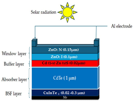
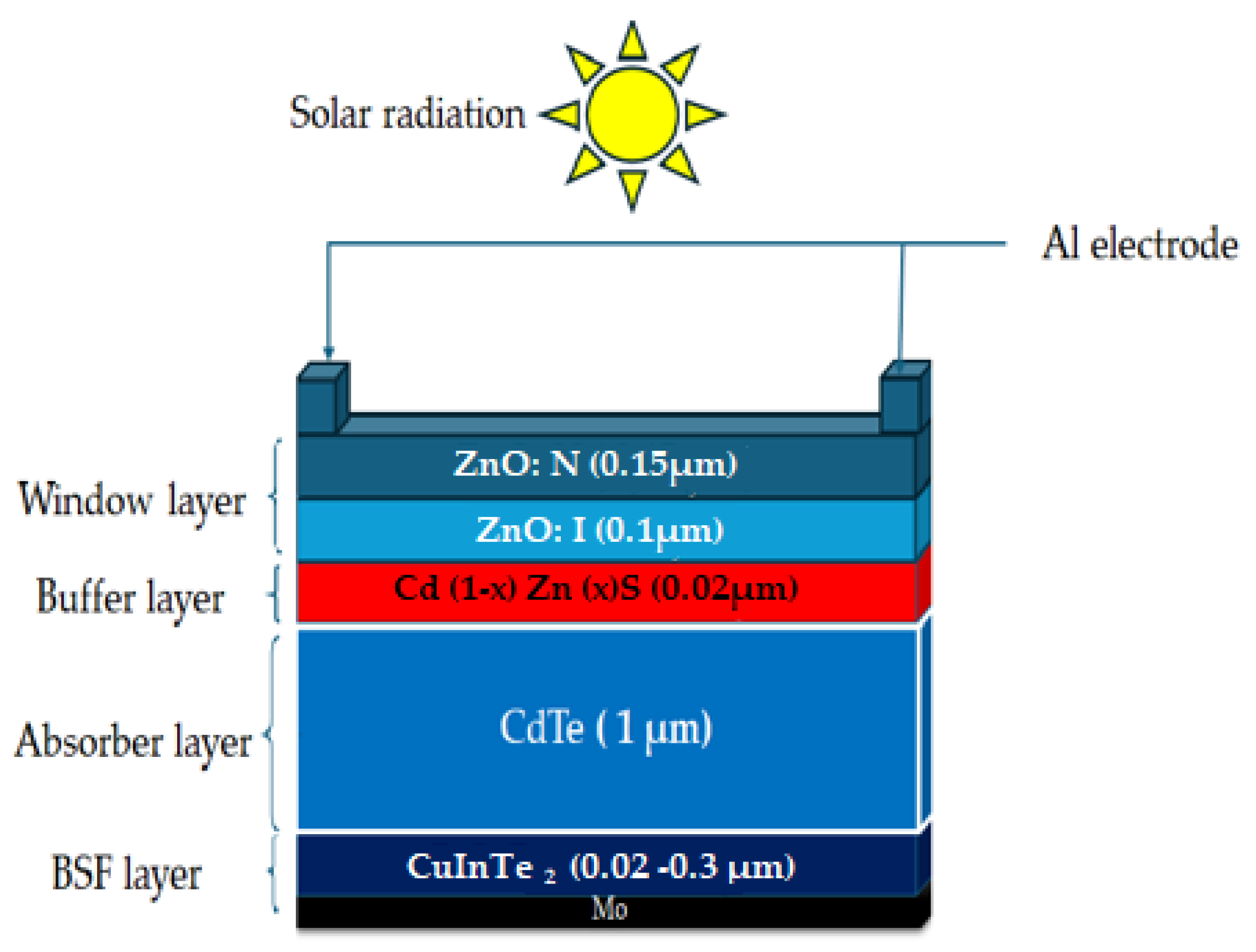
Figure 1 shows the configuration of the simulated structure. The structure consists of a substrate, a back contact, an absorber, a buffer layer, a window layer, and a front contact. First, a layer of molybdenum is sputtered onto glass to form the back contact. Next, a Copper Indium Ditelluride (CIT) P-type booster current layer is added, followed by a CdTe absorber and a Cd(1−x)Zn(x)S buffer layer. The latter has a direct bandgap and n-type conductivity. In this simulation, the bandgap and electron affinities of the buffer alloy Cd(1−x)Zn(x)S, as well as the thickness of the CuInTe2 layer, are considered variable parameters. The doping density in the buffer layer must exceed that of the absorber by a sufficient amount to confine the space charge region at the absorber, where the electric field helps separate charge carriers [37]. Next, a transparent conductive oxide (TCO) is deposited. Its high direct bandgap of 3.3 eV allows a large number of photons to reach the absorber layer. The TCO constitutes the front contact. A thin, highly resistive ZnO layer is typically positioned between the TCO and the buffer layer.
Figure 1.
Schematic view of our CdTe solar cell structure.
Table 2 summarizes the parameters of the different layers used to model the solar cell, taken from literature values and experimental data [38,39,40].
Table 2.
Input parameters used in numerical analysis [38,39,40].
3. Results and Discussion
3.1. Effect of Cd(1−x)Zn(x)S Buffer Layer
One efficient method for enhancing the performance of CdTe-based solar cells is to incorporate zinc into the CdS buffer layer.
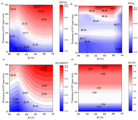
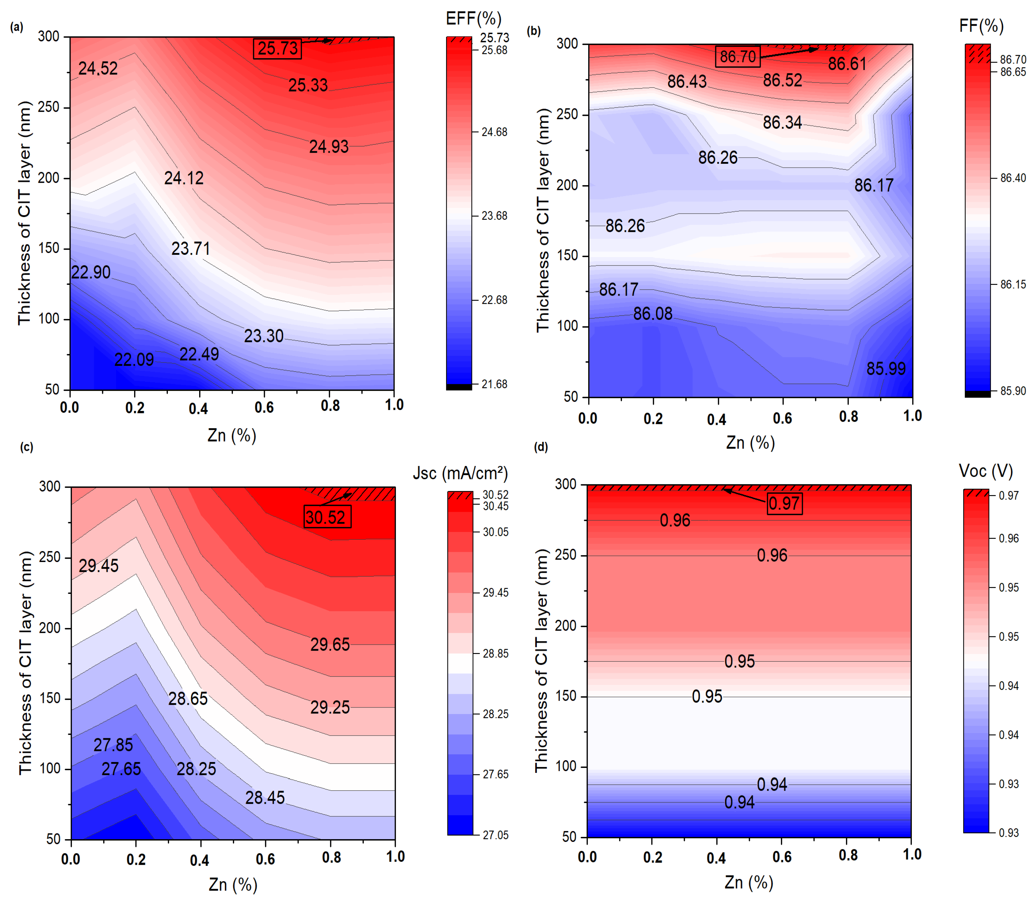
As illustrated in (Figure 2c), the short-circuit current first decreases for Zn concentrations below 0.2, and then significantly increases until Zn = 1. The unfavorable alignment of the conduction and valence bands at the Cd(1−x)Zn(x)S/CdTe interface can be used to explain the initial drop in current for low Zn content from CdS to Cd0.8Zn0.2S. Interface recombination is greatly increased by the energy barriers introduced by this unalignment. In this instance, a higher density of trap states is developed at the Cd(1−x)Zn(x)S/CdTe interface.
Figure 2.
Simulated performance parameters of CdTe solar cell As a function of Zn content and thickness of CIT layer: (a) EFF, (b) FF, (c) Jsc and (d) Voc.
This higher density of trap states causes photogenerated carrier recombination and lowers the collected current. The progressive improvement in the current above 0.2 of zinc is due to the gradual adaptation of the band alignment. As the zinc concentration increases, several advantageous factors become effective. At first, better band alignment between Cd(1−x)Zn(x)S and a more suitable match with CdTe occur, which reduce energy barriers at the interface.
However, it also decreases the density of active trap states at the Cd(1−x)Zn(x)S/CdTe interface. Zinc addition can also improve electronic transport properties in the buffer layer, facilitating carrier collection. (Figure 2d) shows the evolution of the open-circuit voltage (Voc) as a function of the Zn concentration in the Cd(1−x)Zn(x)S layer. It stays practically unchanged, at approximately 0.97 V, for the whole Zn range from 0 to 1. Adding zinc (Zn) to cadmium zinc sulfide Cd(1−x)Zn(x)S mainly changes the properties of the buffer layer. It only has an effect on the cadmium telluride (CdTe) gap, which indicates that the variation in Zn in Cd(1−x)Zn(x)S does not significantly modify the volume recombination in CdTe. That corresponds to passivation of the interfaces and a low density of volume defects, which could otherwise affect Voc.
As shown in Figure 2b, the fill factor (FF) varies only slightly with Zn content at a fixed CIT thickness (e.g., from ~86.5% to ~86.7% at 300 nm), indicating that FF plays only a secondary role in the efficiency enhancement. This near-invariance suggests that junction quality series resistance, shunt resistance, and diode ideality is not substantially altered by moderate Zn incorporation. The slight local dip observed near Zn = 0.2 is consistent with the same trap-state formation and band-offset mismatch discussed above for Jsc, while the subsequent recovery reflects the improved Cd(1−x)Zn(x)S/CdTe band alignment beyond this composition. (Figure 2a) shows the conversion efficiency. Based on the previous interpretation, we can see a close relationship between JSC and EFF.
We can also observe that the efficiency decreases slightly in the Zn < 0.2 region. This is due to the simultaneous decrease in short-circuit current (Jsc) and form factor (FF), caused by increased recombination at the interfaces or band misalignment. Efficiency then improves markedly in the Zn = 0.2 to 0.8% range carrier collection and goes up due to the interface quality being greater, and CdTe absorbs in the ultraviolet and blue regions of the sun’s spectrum. After that, for the range Zn = 0.8 to 1%, efficiency reaches its peak and then remains relatively stable; this means that the cell has reached the best carrier collecting. But for ZnS, this could cause additional defects that make conversion even less efficient.
This confirms that the efficiency trend closely follows Jsc rather than FF, identifying Jsc driven by reduced parasitic absorption and improved band alignment as the dominant contributor to the Zn-related efficiency gain.
3.2. Effect of BSF (CuInTe2) Layer
The CuInTe2 layer goes between the CdTe absorber and the back contact. This is a common setup for a Back Surface Field (BSF), which is used to make the electrical properties of the solar cell’s back interface better. The P-doped CIT layer(CuInTe2) lets holes through but keeps electrons out (which are the minority carriers in P-type CdTe). This forces electrons into the middle of the absorber and prevents their recombination at the back surface.
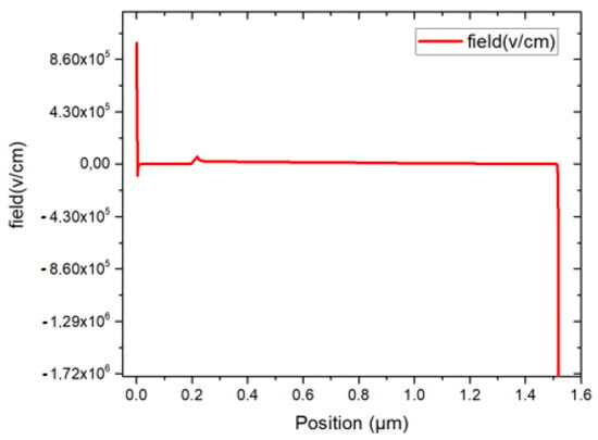
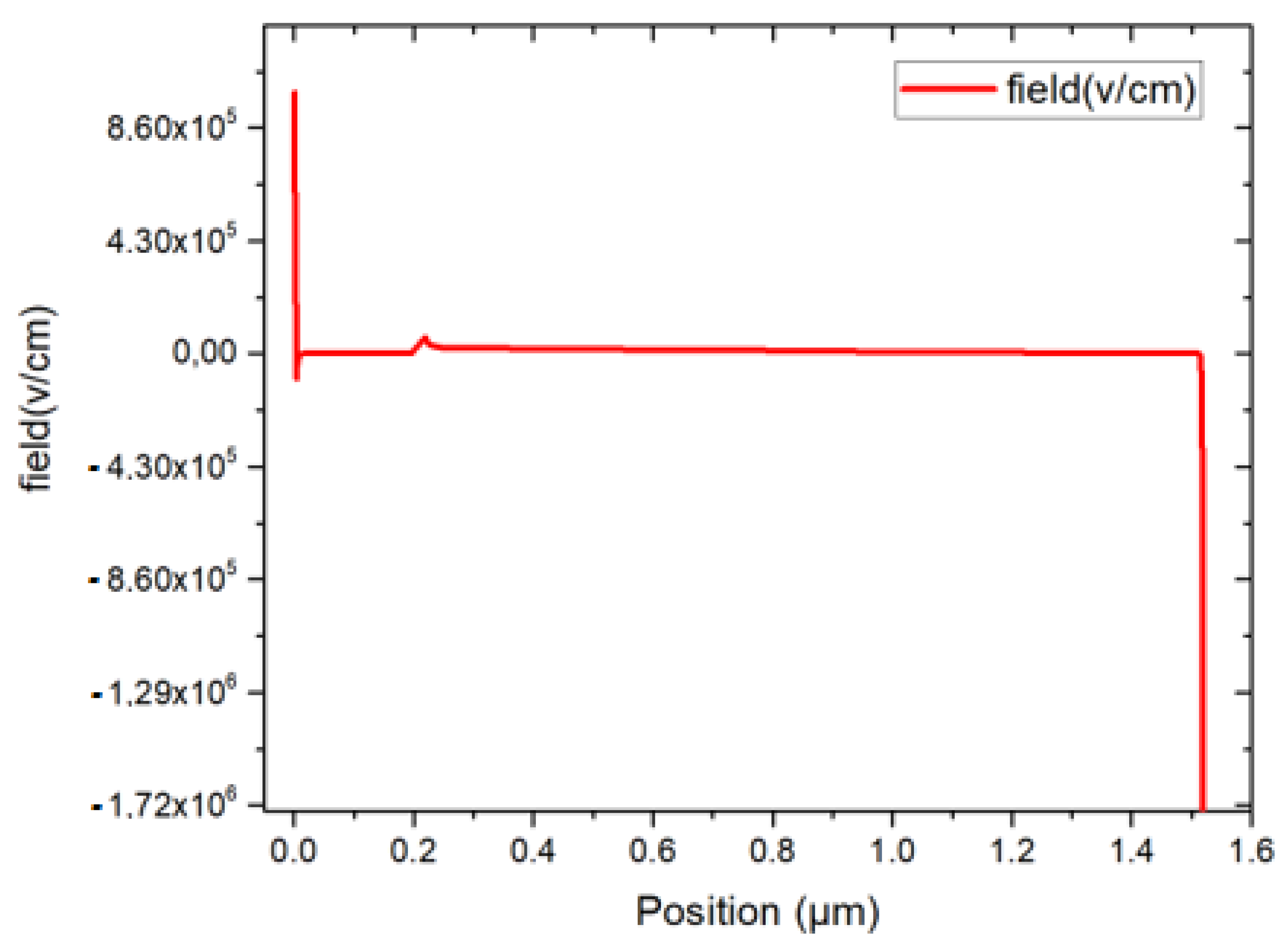
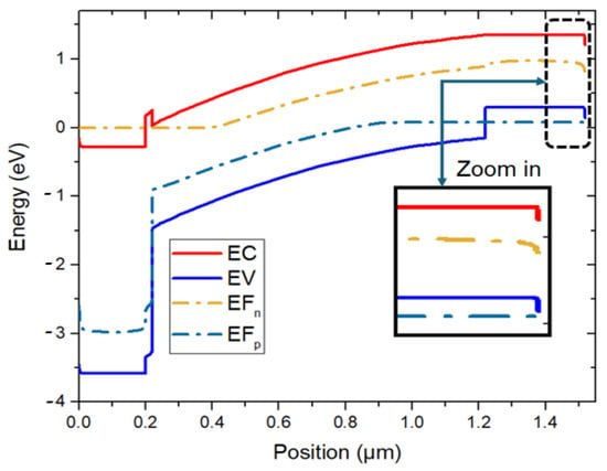
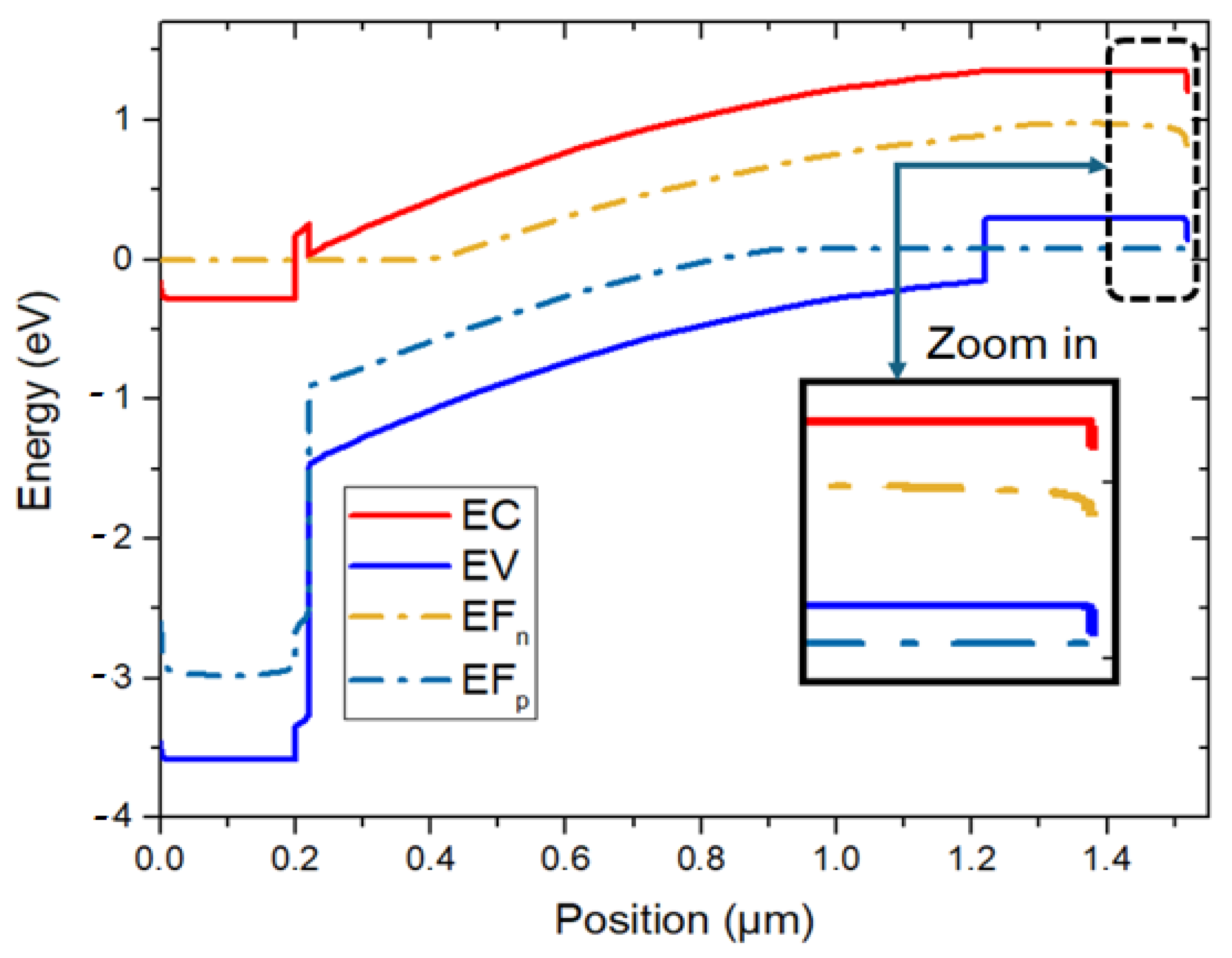
The recombination of minority carriers (electrons) at the back interface is a significant source of loss in CdTe solar cells. The CuInTe2 layer generates a localized electric field through its high doping that repels electrons into the absorber, as seen in Figure 3, thereby reducing the probability of surface recombination. It should be noted that this mechanism does not result from a discontinuity in electronic affinity between CdTe and CIT, since the two layers have virtually identical electronic affinities (4.28 eV, Table 2). However, the CIT layer forms a p+/p junction with the CdTe absorber, due to its significantly higher acceptor doping concentration (NA = 1020 cm−3) compared with 1016 cm−3 in CdTe. This difference in doping produces a narrow and highly localized band bending, confined to the immediate vicinity of the CIT/MO interface (Figure 4), which establishes an internal electrostatic field that repels minority electrons whilst facilitating the transport of majority carriers (holes) towards the back contact, which is consistent with the well-established BSF mechanisms reported for top-bottom junctions in thin-film photovoltaic devices [41,42,43].
Figure 3.
Simulated field of best case XZn = 0.8/thickness CIT = 300 nm.
Figure 4.
Simulated band diagram of the CdTe/CIT/Mo rear-contact region (zoom on the 1.4–1.55 µm interval) showing the localized band bending associated with the highly doped CIT layer.
This effect is enhanced by reducing the interface state density (passivation), which decreases the number of available recombination centers at the rear surface. The CuInTe2 layer increases the lifetime of minority carriers by limiting recombination. This allows more carriers to reach the junction and be collected, thereby improving the photogenerated current and, consequently, the cell efficiency. The introduction of the CIT layer results in a significant increase in open-circuit voltage (Voc), fill factor (FF), and overall cell efficiency Figure 2.
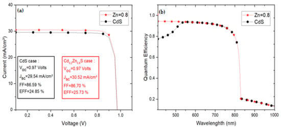
For example, in the case of Zn = 0.8, simulations reveal that efficiency rises from 22.72% (with CIT 50 nm) to 25.73% (with CIT 300 nm), with a Voc of 0.97 V, FF of 86.70%, and short-circuit current density (Jsc) of 30.52 mA/cm2. These gains are related to better carrier collection and lower recombination losses at the back interface. The CuInTe2 layer functions as a passivation layer that reduces defect density at the back interface and improves energy band alignment. The CIT layer creates a potential gradient that favors hole transport to the back contact and electron repulsion in the absorber. This is crucial to avoiding the formation of energy barriers that would limit carrier transport and increase recombination. The simulations indicate that the thickness of the CIT layer is a key parameter, not because the amplitude of the electric field at the back interface increases indefinitely with layer thickness, but because this thickness determines whether the heavily doped BSF region is sufficiently extensive to establish and maintain the electrostatic potential distribution necessary for effective carrier selectivity. In a (p+/p) junction such as that formed at the CdTe/CIT interface, the thickness-dependent behavior observed in our simulations is interpreted as an electrostatic effect related to the thinness of the CIT layer, combined with the ability of the heavily doped BSF layer to maintain the potential distribution at the rear junction, Choe et al. [44] reported that the doping concentration of the BSF layer has a stronger influence on the solar cell’s efficiency than the thickness of this layer.
3.3. The CdTe Solar Cell Optimization
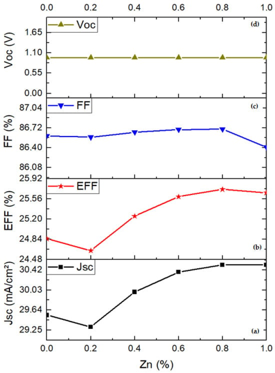
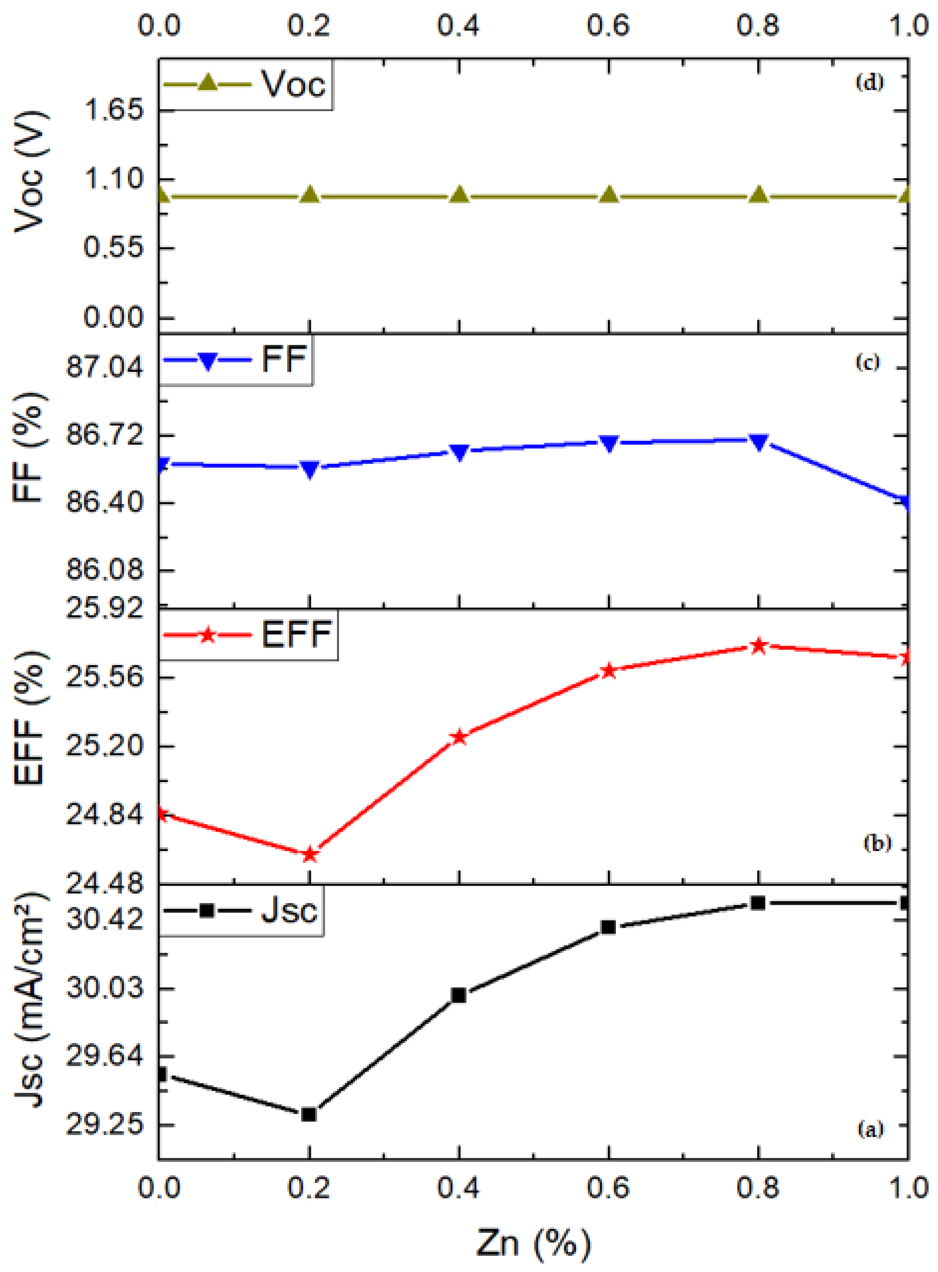
The incorporation of zinc into the CdS buffer layer of CdTe-based solar cells significantly enhances their performance. The bandgap of Cd(1−x)Zn(x)S ranges from 2.4 to 3.7 eV, depending upon the zinc content. The increased gap reduces parasitic absorption in the ultraviolet and blue regions of the spectrum, hence enhancing light transmission to the CdTe absorber layer and resulting in higher photocurrent efficiency (Figure 7b). The band alignment at the CdTe interface has been enhanced. However, with zinc concentrations below 0.2%, the short-circuit current falls, mostly due to band misalignment and higher recombination at the interface. Above this value, band alignment gradually improves, reducing energy barriers and the density of trap states, thus assisting charge carrier collection. Open-circuit voltage stays steady at roughly 0.97 V, minimally impacted by zinc change in the buffer layer. As for the fill factor, it peaks at a zinc concentration of roughly 0.8%, then declines slightly, which may be explained by a degradation in junction quality or higher recombination at the interface. Conversion efficiency consequently leads to a rise in the short-circuit current, as seen in Figure 5.
Figure 5.
Simulated output parameters ((a) Jsc, (b) EFF, (c) FF and (d) Vco) of the studied structure as a function of Zn content for CIT layer of 300 nm.
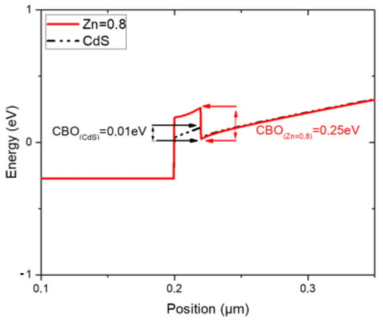
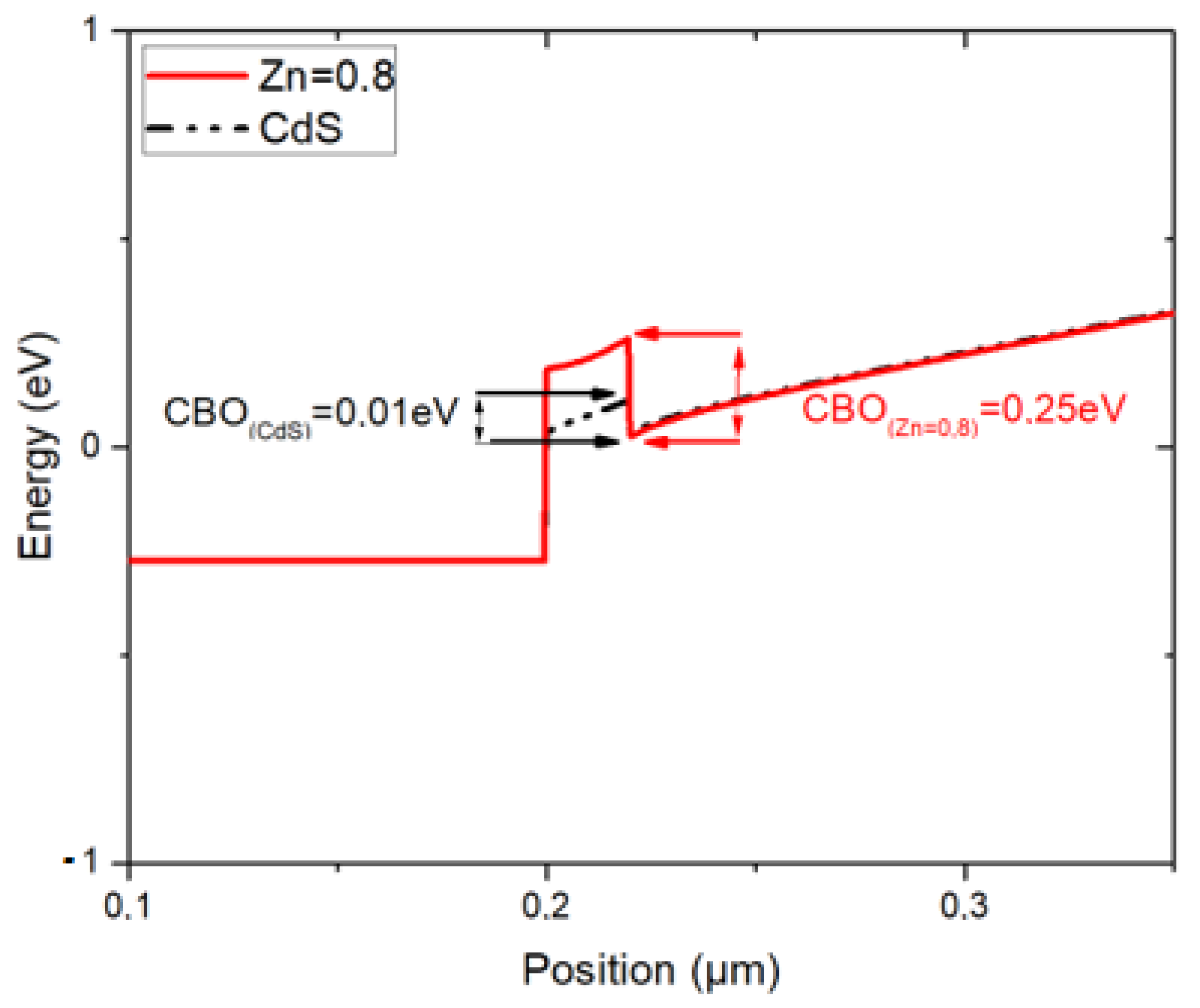
The CBO (conduction band offset) refers to the conduction band minimum of the buffer layer Cd(1−x)Zn(x)S and the minimum energy gap of the absorber (CdTe) at their interface. This parameter is significant because it influences the extent to which photogenerated electrons can move freely from the buffer layer to the absorber, directly affecting the efficiency of the solar cell. There are three possible scenarios. First, if the CBO is too negative (often referred to as a negative spike or cliff), it creates a potential well that favors electron recombination at the interface, leading to a reduction in the open-circuit voltage (Voc) and the overall efficiency of the cell. Second, if the CBO is too positive (a positive spike), it forms a barrier that inhibits electrons from traveling through the interface, which limits the short-circuit current (Jsc) and consequently reduces efficiency.
Finally, the ideal configuration is characterized by a small positive CBO, which is typically measured in the range of 0.1 to 0.3 eV. This condition allows for optimal electron recombination while still facilitating efficient electron transport, resulting in the best performance of the solar cell, according to prior research [13,36].
In this work, we varied the concentration of Zn in Cd(1−x)Zn(x)S. This variation affects the CBO and tunes the lower conduction band of the buffer layer, thereby adjusting the CBO to CdTe. Figure 6 shows the standard case of CdS with a CBO of about 0.01 eV and the optimal case (Zn = 0.8) with 0.25 eV. The latter is considered a value that allows for the best compromise between reduced recombination and efficient carrier transport as we see in J (V) Characteristic curve on (Figure 7a).
Figure 6.
Simulated Band Conduction Offset (CBO) of CdS case and the optimized cell with (XZn = 0.8).
Figure 7.
(a) J (V) Characteristic curve and (b) quantum efficiency for the CdTe solar cell with CdS buffer layer and the optimized cell with (Cd0.2Zn0.8S) buffer layer.
4. Conclusions
Our work has demonstrated that a dual-interface passivation approach, which combines a front buffer layer of Cd(1−x)Zn(x)S with a rear surface field layer of CuInTe2, is an effective method for producing high-efficiency, ultra-thin CdTe solar cells. Simulations using the wxAMPS-1D 3.0 software have shown that increasing the Zn content widens the bandgap of the buffer layer and improves band alignment at the buffer/absorber interface, which increases the short-circuit current (Jsc) and the fill factor (FF), and that the introduction of the CuInTe2 layer at the back contact proved to be crucial: for a fixed Zn content of 0.8, increasing its thickness from 50 to 300 nm increased the efficiency from 22.72% to 25.73% by reducing recombination at the back contact and facilitating hole collection.
The optimal configuration identified (Zn = 0.8, CIT thickness = 300 nm) yields Jsc = 30.52 mA/cm2, Voc = 0.97 V, FF = 86.70%, and a conversion efficiency of 25.73%, with a CdTe absorber only 1 µm thick. This efficiency is significant compared to previous front- or back-passivation approaches reported in the literature. Beyond electrical performance, reducing the CdTe thickness to 1 µm well below the standard industrial range of 3 to 5 µm lowers the consumption of tellurium and cadmium, directly addressing concerns regarding material costs and toxicity that currently limit the large-scale deployment of CdTe photovoltaic systems.
Several perspectives remain open for future work. First, replacing the uniform Cd(1−x)Zn(x)S composition with a graded Zn profile across the entire thickness of the buffer layer (higher near the front contact, lower near the CdTe) could smooth the bandgap transition and further reduce interfacial recombination. Alternatively, investigating other candidates for the BSF role, such as CuGaTe2, CuInSe2, or Cu(In,Ga)Te2 alloys, could be compared to CuInTe2 within the same simulation framework.
Author Contributions
Conceptualization, S.A.E.M.A.; methodology, Y.Z.H. and S.A.E.M.A.; software, Y.Z.H.; validation, Y.Z.H. and S.A.E.M.A.; formal analysis, Y.Z.H. and S.A.E.M.A.; investigation, Y.Z.H. and S.A.E.M.A.; resources, Y.Z.H.; data curation, Y.Z.H.; writing—original draft preparation, Y.Z.H.; writing—review and editing, S.A.E.M.A.; visualization, Y.Z.H. and S.A.E.M.A.; supervision, S.A.E.M.A.; project administration, S.A.E.M.A.; funding acquisition, S.A.E.M.A. All authors have read and agreed to the published version of the manuscript.
Funding
This research received no external funding.
Data Availability Statement
Data will be made available on request.
Conflicts of Interest
The authors declare no conflict of interest.
References
- Zhang, Y. Solar PV in the 21st Century: Aligning Technological Growth with Sustainability. Energy 2026, 10, 100499. [Google Scholar] [CrossRef] [Scilit]
- Hassan, M.; Mohamed, E.; Kamel, S.; Ardjoun, S.A.E.M. Stochastic Optimal Power Flow Integrating with Renewable Energy Resources and V2G Uncertainty Considering Time-Varying Demand: Hybrid GTO-MRFO Algorithm. IEEE Access 2024, 12, 97893–97923. [Google Scholar] [CrossRef] [Scilit]
- Ibrahim, N.F.; Ardjoun, S.A.E.M.; Alharbi, M.; Alkuhayli, A.; Abuagreb, M.; Khaled, U.; Mahmoud, M.M. Multiport Converter Utility Interface with a High-Frequency Link for Interfacing Clean Energy Sources (PV\Wind\Fuel Cell) and Battery to the Power System: Application of the HHA Algorithm. Sustainability 2023, 15, 13716. [Google Scholar] [CrossRef] [Scilit]
- Priyadarshini, M.; Mahmoud, M.M.; Sur, U.; Ardjoun, S.A.E.M.; Hysa, A.; Bessous, N.; Metwally, K.; Anwer, N. Microcontroller-Based Prototype Model of a Solar Wireless Electric Vehicle-to-Vehicle Charging System with Real-Time Battery Voltage Monitoring. Bul. Ilm. Sarj. Tek. Elektro 2025, 7, 527–540. [Google Scholar] [CrossRef]
- Ardjoun, S.A.E.M.; Denaï, M.; Chafouk, H. A Robust Control Approach for Frequency Support Capability of Grid-Tie Photovoltaic Systems. J. Sol. Energy Eng. 2022, 145, 021009. [Google Scholar] [CrossRef] [Scilit]
- Thinn, K.T.; Saeed, W. Consensus and Divergence in Explainable AI (XAI): Evaluating Global Feature-Ranking Consistency with Empirical Evidence from Solar Energy Forecasting. Mathematics 2026, 14, 297. [Google Scholar] [CrossRef] [Scilit]
- Priyadarshini, M.; Ardjoun, S.A.E.M.; Hysa, A.; Mahmoud, M.M.; Sur, U.; Anwer, N. Time-Domain Simulation and Stability Analysis of a Photovoltaic Cell Using the Fourth-Order Runge-Kutta Method and Lyapunov Stability Analysis. Bul. Ilm. Sarj. Tek. Elektro 2025, 7, 214–230. [Google Scholar] [CrossRef]
- Ibrahim, N.F.; Mahmoud, M.M.; Alnami, H.; Wapet, D.E.M.; Ardjoun, S.A.E.M.; Mosaad, M.I.; Hassan, A.M.; Abdelfattah, H. A New Adaptive MPPT Technique Using an Improved INC Algorithm Supported by Fuzzy Self-Tuning Controller for a Grid-Linked Photovoltaic System. PLoS ONE 2023, 18, e0293613. [Google Scholar] [CrossRef] [Scilit] [PubMed]
- Elbahri, M.; Taleb, N.; Fahsi, M.; Taousser, F.; Ardjoun, S.A.E.M. A Lightweight Autoencoder for Photovoltaic Module Defect Segmentation from Electroluminescence Images. Sol. Energy 2026, 307, 114362. [Google Scholar] [CrossRef] [Scilit]
- Oviedo, F.; Ren, Z.; Hansong, X.; Tian, S.I.P.; Zhang, K.; Layurova, M.; Heumueller, T.; Li, N.; Birgersson, E.; Sun, S.; et al. Bridging the Gap between Photovoltaics R&D and Manufacturing with Data-Driven Optimization. arXiv 2020, arXiv:2004.13599. [Google Scholar]
- Slimani, M.A.; Wadhwa, A.; Gerlein, L.F.; Benavides-Guerrero, J.A.; Taherian, M.H.; Izquierdo, R.; Cloutier, S.G. Controlling the Optical and Electrical Properties of Perovskite Films and Enhancing Solar Cell Performance Using the Photonic Curing Process. Nanomaterials 2024, 14, 1975. [Google Scholar] [CrossRef] [Scilit] [PubMed]
- Bosio, A.; Rosa, G.; Romeo, N. Past, Present and Future of the Thin Film CdTe/CdS Solar Cells. Sol. Energy 2018, 175, 31–43. [Google Scholar] [CrossRef] [Scilit]
- Hamri, Y.Z.; Bourezig, Y.; Medles, M.; Ameri, M.; Toumi, K.; Ameri, I.; Al-Douri, Y.; Voon, C.H. Improved Efficiency of Cu(In,Ga)Se2 Thinfilm Solar Cells Using a Buffer Layer Alternative to CdS. Sol. Energy 2019, 178, 150–156. [Google Scholar] [CrossRef] [Scilit]
- Doroody, C.; Rahman, K.S.; Kiong, T.S.; Amin, N. Optoelectrical Impact of Alternative Window Layer Composition in CdTe Thin Film Solar Cells Performance. Sol. Energy 2022, 233, 523–530. [Google Scholar] [CrossRef] [Scilit]
- Manoua, M.; Liba, A. Optimization and Performance Analysis of N-ZnO/p-CdTe Thin Heterojunction Solar Cells via Two-Dimensional Numerical Simulation. Results Opt. 2025, 18, 100761. [Google Scholar] [CrossRef] [Scilit]
- Ahmad, N.I.; Kiong, T.S.; Doroody, C.; Rahman, K.S.; Norizan, M.N.; Ahmad, M.F.; Kar, Y.B.; Harif, M.N.; Amin, N. Copper Doping Effect in the Back Surface Field Layer of CdTe Thin Film Solar Cells. Alex. Eng. J. 2024, 88, 155–163. [Google Scholar] [CrossRef] [Scilit]
- Ranjan, R.; Kumar, A.; Bhardwaj, N.; Atul, A.K.; Tiwari, R.N.; Sharma, A.K.; Srivastava, N. Impact of Tin-Based Perovskite as a Hole Transport Layer on the Device Performance of Stable and 27.10% Efficient CdTe-Based Solar Cell by Numerical Simulation. J. Phys. Chem. Solids 2023, 181, 111546. [Google Scholar] [CrossRef] [Scilit]
- Mukhtar, M.; Artegiani, E.; Torabi, N.; Anefnaf, I.; Nicole Barrantes, J.J.; Meneghini, M.; Romeo, A. Study of Ultra-Thin Cadmium Telluride Solar Cells; Institute of Electrical and Electronics Engineers Inc.: New York, NY, USA, 2024. [Google Scholar]
- Artegiani, E.; Punathil, P.; Kumar, V.; Bertoncello, M.; Meneghini, M.; Gasparotto, A.; Romeo, A. Effects of CdTe Selenization on the Electrical Properties of the Absorber for the Fabrication of CdSexTe1-x/CdTe Based Solar Cells. Sol. Energy 2021, 227, 8–12. [Google Scholar] [CrossRef] [Scilit]
- Kapadnis, R.S.; Bansode, S.B.; Supekar, A.T.; Bhujbal, P.K.; Kale, S.S.; Jadkar, S.R.; Pathan, H.M. Cadmium Telluride/Cadmium Sulfide Thin Films Solar Cells: A Review. ES Energy Environ. 2020, 10, 3–12. [Google Scholar] [CrossRef] [Scilit]
- Demtsu, S.H.; Sites, J.R. Effect of Back-Contact Barrier on Thin-Film CdTe Solar Cells. Thin Solid Films 2006, 510, 320–324. [Google Scholar] [CrossRef] [Scilit]
- Jia, G.; Liu, B.; Wang, K.; Wang, C.; Yang, P.; Liu, J.; Zhang, W.; Li, R.; Zhang, S.; Du, J. CuInTe2 Nanocrystals: Shape and Size Control, Formation Mechanism and Application, and Use as Photovoltaics. Nanomaterials 2019, 9, 409. [Google Scholar] [CrossRef] [Scilit] [PubMed]
- Kuhaimi, S.A.A. Conduction and Valence Band Offsets of CdS/CdTe Solar Cells. Energy 2000, 25, 731–739. [Google Scholar] [CrossRef] [Scilit]
- Zaidi, B.; Houaidji, N.; Khadraoui, A.; Gagui, S.; Shekhar, C.; Ozen, Y.; Kamli, K.; Hadef, Z.; Donmez, M.; Comert, B.; et al. Structural, Optical and Electrical Properties of Zn x Sn 1-x S Thin Films Deposited by Chemical Spray Pyrolysis. J. Nano Res. 2022, 61, 72–77. [Google Scholar]
- Aktar, S.; Paul, D.; Tamang, A.; Chattopadhyay, B. Quantum Size Effect of CdS Quantum Dot as Electron Transport Layer for Enhanced Performance in CdTe Based Solar Cells. J. Phys. Chem. Solids 2026, 208, 113173. [Google Scholar] [CrossRef] [Scilit]
- Shang, J.; Murugesan, M.; Sartor, B.E.; Lott, H.; Duenow, J.N.; Young, M.; McCloy, J.S. Design and Simulation of N-Type Solar Cells Based on an Iodine-Doped CdTe Absorber Using SCAPS-1D. Mater. Sci. Semicond. Process. 2026, 208, 110527. [Google Scholar] [CrossRef] [Scilit]
- Harif, M.N.; Doroody, C.; Nadzri, A.; Nisham Rosly, H.; Ahmad, N.I.; Isah, M.; Amin, N. Effect of Cu2Te Back Surface Interfacial Layer on Cadmium Telluride Thin Film Solar Cell Performance from Numerical Analysis. Crystals 2023, 13, 848. [Google Scholar] [CrossRef] [Scilit]
- Suthar, D.; Sharma, V.; Vaishnav, H. Modeling of High Efficiency CdTe Solar Cells with MgZnO as Window Layer by Using SCAPS-1D Simulation Approach. Russ. J. Gen. Chem. 2026, 96, 207. [Google Scholar] [CrossRef] [Scilit]
- V, V.N.; Rajni, K.S.; Jena, I.; Singh, U.P. Efficiency Enhancement of CdTe Solar Cells Using Cu2MnSnS4 Back Contact Layer: -Experimental and Numerical Analysis. Renew. Energy 2026, 260, 125183. [Google Scholar] [CrossRef] [Scilit]
- Carranza, A.C.; Rosendo, E.; Zepeda, J.C.; Morales, C.; Camacho, E.; Treviño, L.; García, G.; Romano, R.; Coyopol, A.; Galeazzi, R. Theoretical Optimization of Environmentally Friendly Alternative Indium-Doped Zinc Oxide (IZO) in CdTe Solar Cell Technology by SCAPS-1D. Trans. Electr. Electron. Mater. 2026, 27, 510–522. [Google Scholar] [CrossRef] [Scilit]
- Kc, D.; Shah, D.K.; Akhtar, M.S.; Park, M.; Kim, C.Y.; Yang, O.-B.; Pant, B. Numerical Investigation of Graphene as a Back Surface Field Layer on the Performance of Cadmium Telluride Solar Cell. Molecules 2021, 26, 3275. [Google Scholar] [CrossRef] [Scilit] [PubMed]
- Liu, Y.; Sun, Y.; Rockett, A. A New Simulation Software of Solar Cells—WxAMPS. Sol. Energy Mater. Sol. Cells 2012, 98, 124–128. [Google Scholar] [CrossRef] [Scilit]
- Narimani, M.; Abbasian, K.; Kiani, G. Analysis of wxAmps Results for a New Dye Sensitized Solar Cell Using Solid State Electrolyte and Graphene. Int. J. Comput. Sci. Netw. Secur. 2024, 24, 164–168. [Google Scholar] [CrossRef]
- Adaikalam, K.; Valanarasu, S.; Ramesh, S.; Kim, H.S.; Kim, H.-S. Photoelectrochemical Solar Cell Study of Electrochemically Synthesized Cd1-xZnxTe Thin Films. Sol. Energy 2021, 224, 923–929. [Google Scholar] [CrossRef] [Scilit]
- Chander, S.; Dhaka, M.S.; De, A.K.; Kaur, I. Evolution of Treated CdS/CdZnTe Interface Structures for CdZnTe Based Solar Cells. Sol. Energy Mater. Sol. Cells 2026, 296, 114066. [Google Scholar] [CrossRef] [Scilit]
- Wen, J.; Zhang, F.; Yu, Q.; Zhao, Y. The Study of AgInS2 Solar Cell Using Simulation Software wxAMPS. Opt. Mater. 2022, 134, 112867. [Google Scholar] [CrossRef] [Scilit]
- Moutinho, H.R.; Johnston, S.; To, B.; Jiang, C.-S.; Xiao, C.; Hacke, P.; Moseley, J.; Tynan, J.; Dhere, N.G.; Al-Jassim, M.M. Development of Coring Procedures Applied to Si, CdTe, and CIGS Solar Panels. Sol. Energy 2018, 161, 235–241. [Google Scholar] [CrossRef] [Scilit]
- Xu, X.-B.; Wang, X.-Y.; Gu, W.-P.; Quan, S.; Zhang, Z. Study on Influences of CdZnS Buffer Layer on CdTe Solar Cells. Superlattices Microstruct. 2017, 109, 463–469. [Google Scholar] [CrossRef] [Scilit]
- Hossain, S.; Pappu, M.; Mondal, B.K.; Abir, A.; Hossain, J. Highly Efficient CdTe Solar Cell with a Thin CIT Current Booster: Theoretical Insights. arXiv 2023, arXiv:2308.00349. [Google Scholar]
- Hashmi, G.; Hossain, S.; Rashid, M.J. Simulation of CdTe, CIGS and CZTS Solar Cells Using WxAMPS Software. Res. Sq. 2021; preprints.
- Kumar, A.; Thakur, A.D. Role of Contact Work Function, Back Surface Field, and Conduction Band Offset in Cu2ZnSnS4 Solar Cell. Jpn. J. Appl. Phys. 2018, 57, 08RC05. [Google Scholar] [CrossRef] [Scilit]
- Gorai, P.; Krasikov, D.; Grover, S.; Xiong, G.; Metzger, W.K. Stevanović A Search for New Back Contacts for CdTe Solar Cells. Sci. Adv. 2023, 9, eade3761. [Google Scholar] [CrossRef] [Scilit] [PubMed]
- Hossain, M.; Amin, N.; Razykov, T.M. Prospects of Back Contacts with Back Surface Fields in High Efficiency ZnxCd1-xS/CdTe Solar Cells from Numerical Modeling. Chalcogenide Lett. 2011, 8, 187. [Google Scholar]
- Choe, K.S. Parametric Simulation of the Back-Surface Field Effect in the Silicon Solar Cell. Solid State Sci. 2014, 29, 48–51. [Google Scholar] [CrossRef] [Scilit]

Disclaimer/Publisher’s Note: The statements, opinions and data contained in all publications are solely those of the individual author(s) and contributor(s) and not of MDPI and/or the editor(s). MDPI and/or the editor(s) disclaim responsibility for any injury to people or property resulting from any ideas, methods, instructions or products referred to in the content. |
© 2026 by the authors. Licensee MDPI, Basel, Switzerland. This article is an open access article distributed under the terms and conditions of the Creative Commons Attribution (CC BY) license.