


Abstract
In this paper, a sharp band-pass filter (BPF) with enhanced pass-band and stop-band specifications is presented. The filter can be utilized for 5G mid-band applications along with LTE42 (3.4–3.6 GHz) and LTE43 (3.6–3.8 GHz) to comply with the standards of different countries. The initial design of the filter consists of a high impedance transmission line connecting the filter’s two ports, which are terminated by 50 Ω resistors. Although this design results in reasonable pass-band characteristics, its stop-band and transition-band characteristics are relatively weak. Due to this shortcoming, the stop-band and transition-band characteristics of the filter are improved by locating sharp transmission zeros within the stop-band to determine the filter bandwidth and to significantly increase the stop-band attenuation. These modifications are achieved by inserting a pair of shunt short- and open-circuit stubs, a pair of short-circuited U-shaped parasitic elements, and a central short-circuited U-shaped element. The filter is mathematically analyzed and modeled, and the design steps are also demonstrated. The simulation and measured results are compatible, and the measurements show an insertion loss of 0.35 dB, stop-band attenuation larger than 20 dB, sharp transmission zeros, and a transition-band value within 10% of the center frequency.
1. Introduction
The congested spectrum allocation of wireless communications has forced researchers to pay great attention to microwave filter design. Band-pass filters (BPFs) are indispensable components in wireless transmitters and receivers to determine the transmission of communication devices within the frequency band of interest while avoiding interference with other nearby communication systems. Since each frequency band assigned for a certain application is very close to the adjacent bands, the filter passband should cover the intended band with as small an insertion loss as possible. However, the filter transition band should also be negligible, with transmission zeros having very large attenuation. Moreover, the stop-band attenuation should be as large as possible to filter out the adjacent unintended bands. The 5G mid-band applications in different countries have occupied the LTE42 (3.4–3.6 GHz) and the LTE43 (3.6–3.8 GHz) bands, so it is a very wise idea to propose a band-pass filter that efficiently passes these consecutive bands and suppresses the unwanted bands to comply with the requirements of the 5G mid-band applications. Unfortunately, conventional filter designs require a very complicated procedure with large dimensions when the matter of high filter performance is the first intention [1]. Consequently, the researchers have proposed many non-conventional structures to overcome the problem of bulky structures and the complexity of the design steps.
In [2], a compact BPF is designed to operate in 5G mid-band using two squared loops coupled with two T-shaped structures acting as feed lines. It has a compact size but a large transient band and low suppression attenuation. In [3], a BPF is designed to cover 5G mid-band (3.4–3.7 GHz) using three trisection open-loop ring resonators with 50 Ω transmission lines for input/output termination. The authors obtain a compact size and only two transmission zeros in the upper transition band. A low-cost BPF is designed to cover 3.7–4.2 GHz using the Stub Loaded Multiple Mode Resonator (SL-MMR) technique with two parasitic elements [4]. The design has a flat passband with two transmission zeros around the passband. The authors of [5] use a half-mode substrate-integrated rectangular cavity (HMSIRC) to implement a low-loss and broad stop-band BPF response by adding magnetic and electric walls and a transverse slot to the design. Consequently, they present a second-order filter with 0.41 dB insertion loss and a broad stop-band. In [6], a dual-mode high selectivity BPF is designed by a square patch resonator with a periodic metallic via array. The structure produces a four-pole BPF through the cascading of two resonators with a quadrature wavelength microstrip connector in two different ways. The structure represents two BPFs with 5 and 4 transmission zeros, whose resonators produce 2 transmission zeros. A filter that can be used for single-, tri-, or quint-band BPF using a meander-coupled line with a stepped-impedance resonator is presented in [7]. In [8], the authors use a folded-arms square open-loop resonator (FASOLR) to implement a fifth-order Chebyshev BPF with compact size.
In [9], a BPF is designed through a simple three-coupled lines structure loaded by open- and short-circuited stubs to realize low insertion loss with high return loss. The authors in [10] design a compact BPF with a selective suppression band using a circular microstrip dual-coupled dual-tuned structure with two radial stubs that act as a capacitor in the passband and as a series resonator circuit in the stopband. The filter has two transmission zeros, the first at the end of the passband and the second at a certain frequency in the stopband to improve the stopband characteristics. In [11], a compact Chebyshev BPF is presented with low insertion loss and a high suppression band by using asymmetrical cells with a shunt half-wave open-circuit stub in the center of the cell instead of the traditional quadrature wave transformer, also by using folded stepped impedance instead of traditional half-wavelength transmission lines. A cascaded ring resonator and a lumped-element filtering network are used to design a low-insertion-loss, wideband BPF with ultra-stopbands up to 19 times the value of the resonant frequency [12]. In [13], a BPF is designed through a cascaded low-pass filter (LPF) and high-pass filter (HPF) based on the suspended substrate stripline (SSS) technique. Sharp edges are obtained with 1.5 dB insertion loss and high suppression in the stop-band.
In recent years, many papers have used the multi-mode resonator technique to design BPFs, and they include, but are not limited to, the following. In [14], a stub-loaded multiple-mode resonator (SL-MMR) with a half-wavelength resonator folded as a C-shape element is designed by using two pin diodes and a central quadrature wavelength loaded with a short-circuited via. As a result, a switchable BPF is created for 5G, WiMAX, and WLAN applications. In [15], a reconfigurable filtering antenna is created through a cascaded reconfigurable BPF with a UWB cup antenna. An E-shaped multiple-mode resonator (MMR) with a pair of pin diodes and a varactor diode is relied on to create step and continuous tuning. In [16], a multiple-mode resonator (MMR) with stepped impedance short and open circuited stubs is used in [16] to generate a wideband BPF with three transmission zeros. The reconfigurable BPF in [17] is designed through a multi-mode resonator (MMR) with two interdigitally coupled structures and two varactor diodes, producing tuning capability with constant absolute bandwidth.
In [18], the authors design a dual-band BPF by mixing a defected stepped impedance resonator (DSIR) with a microstrip stepped impedance resonator (MSIR), so they obtain a compact size and high selectivity but a high-insertion-loss filter. In [19], a dual-band BPF is designed using loaded open/short-circuited stubs. The design has low insertion loss with a flat passband. However, it still has a wide transition band. A substrate-integrated defected ground structure (SIDGS) is used in [20] to design single- and dual-band BPFs with low loss and a wide stopband with multi-layers and metallic vias from the top layer down to the bottom ground plane. A dual-band BPF is designed in [21] using a cascaded coupled-line section with an open-circuit stub and a stepped-impedance feed line loaded by an open stub to have a wide inter-stop-band between the two pass-bands.
The Substrate Integrated Waveguide (SIW) technique is widely used to design band-pass filters. In [22] SIW is used with an optimized cavity and an H-slot having two poles in order to create a four-pole BPF by two cavities in cascade. Only one varactor diode is used in each cavity to get a tunable BPF with broad stop-band suppression. An SIW with a multi-coupled microstrip resonator loaded with a varactor diode is presented in [23]. The design produces a fully controllable ultra-wideband (UWB) BPF. A circular SIW is used in [24] to design a BPF with three poles and one transmission zero in the upper stopband. In [25], the authors design two fourth-order Chebyshev BPFs using SIW with elliptic stepped impedances acting as impedance inverters.
In [26], a BPF is designed using inductively cross-coupled resonators tuned with varactor diodes, resulting in a triple-tuned microstrip band-pass filter with concurrently tuned transmission zeros on both sides of the passband. The authors in [27] design a high-temperature superconductor wideband BPF using a quintuple mode resonator (QMR), which has transmission zeros surrounding the passband to enhance the selectivity of the filter. In [28], a reflection-less BPF is implemented by mixing two sections of BPF with a stop-band filter (SBF). The structure has an excellent reflection coefficient with low insertion loss, but the bandwidth of the filter is still uncontrollable, with bad transition-band characteristics.
Last year, some papers started using deep learning to design the BPF. In [29], adaptive reconfigurable bandwidth is created based on a deep Q-network (DQN) to provide a two-pole tunable filter. On the other hand, the inverse design method is applied in [30] to obtain a single- and dual-band BPF through deep learning using a compositional pattern producing network (CPPN) with genetic algorithm optimization to optimize the filter structure.
In this paper, a sharp BPF with very low insertion losses in the passband, high attenuation in the stopband, and a narrow transition band is designed and fabricated. The filter consists of a band-pass section to pass the frequency band of interest, whereas the stop-band specifications are improved by shunt stubs and three short-circuited U-shaped parasitic elements. The resulting filter efficiently passes the 5G mid-band applications with high attenuation against the out-of-band frequencies. Although the initial structure starts with the one proposed in [28], the modifications that have been proposed have enhanced the filter performance tremendously. The initial design has a wide transition band with relatively low stop-band attenuation, but the proposed design has a narrow transition band (about 10% of the center frequency) and large stop-band attenuation (larger than 20 dB). Therefore, the filter performance is improved to provide a sharp response while maintaining the pass-band characteristics of the initial design. In addition, the function of each proposed element has been discussed mathematically and graphically in this paper. The measured results are in very good agreement with simulation results, which verify the capability of exploiting the proposed filter for 5G devices. The rest of the paper is organized as follows: Section 2 demonstrates the overall dimensions of the proposed filter and the materials used to fabricate it. Section 3 reveals the design steps that were followed to obtain the final design of the filter. Section 4 delves into the mathematical modeling of the filter. The parameter study is discussed in Section 5 to explain the effect of varying the geometric parameter on the filter response, while the measurement environment and results are presented in Section 6. Finally, Section 7 concludes the main findings of this work.
2. Filter Structure
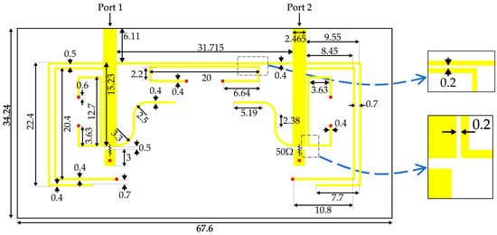
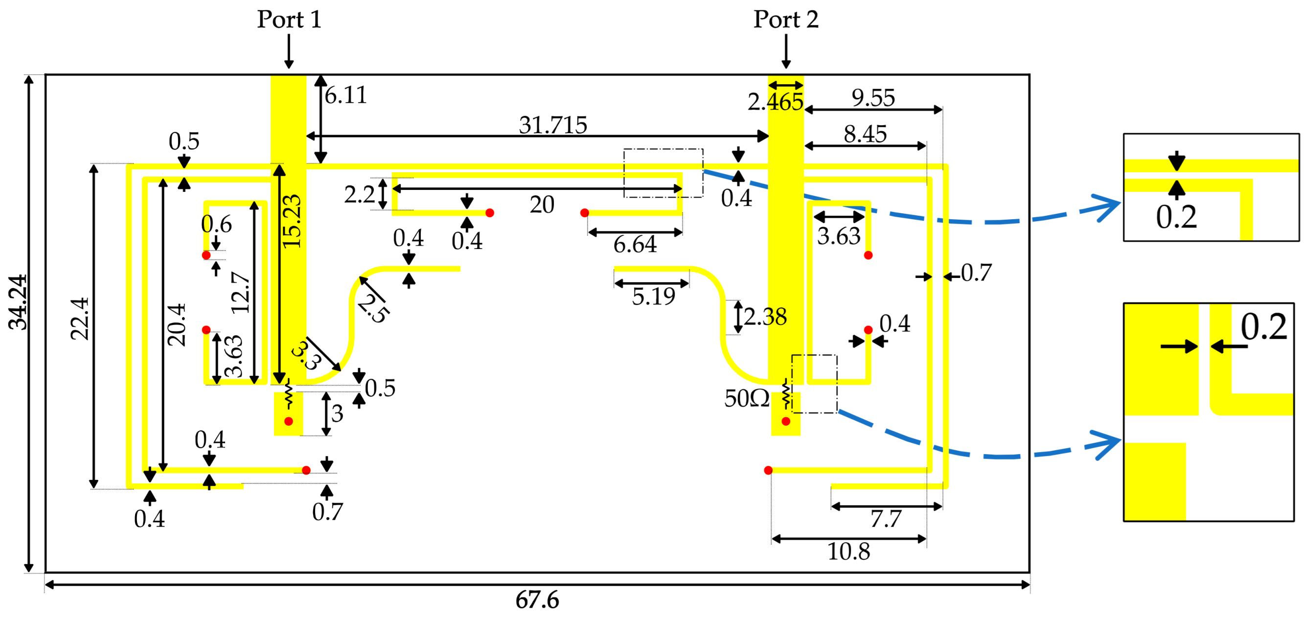
The structure of the proposed filter is illustrated in Figure 1. The top layer of the structure is the copper layer of the filter, while the bottom layer is fully grounded. The two copper layers are isolated by the dielectric substrate. The substrate is a Rogers RT/duroid 5880 with dielectric constant εr = 2.2, loss tangent tan δ = 0.0009, and the substrate height h = 0.8 mm. The red circles in the figure represent the short-circuit via that connects the top copper layer with the ground plane, and its diameter is 0.6 mm.
Figure 1.
Geometry of the proposed filter (all dimensions are in mm).
The main part of the proposed filter is the high-impedance transmission line that connects the two feed lines. This part represents the band-pass section of the entire filter, so it provides an almost flat passband response with the help of the two 50 Ω resistors terminating the feed lines of the filter. The improvement of the stop-band characteristics is achieved with the aid of three U-shaped parasitic elements and two pairs of shunt stubs.
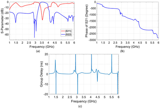
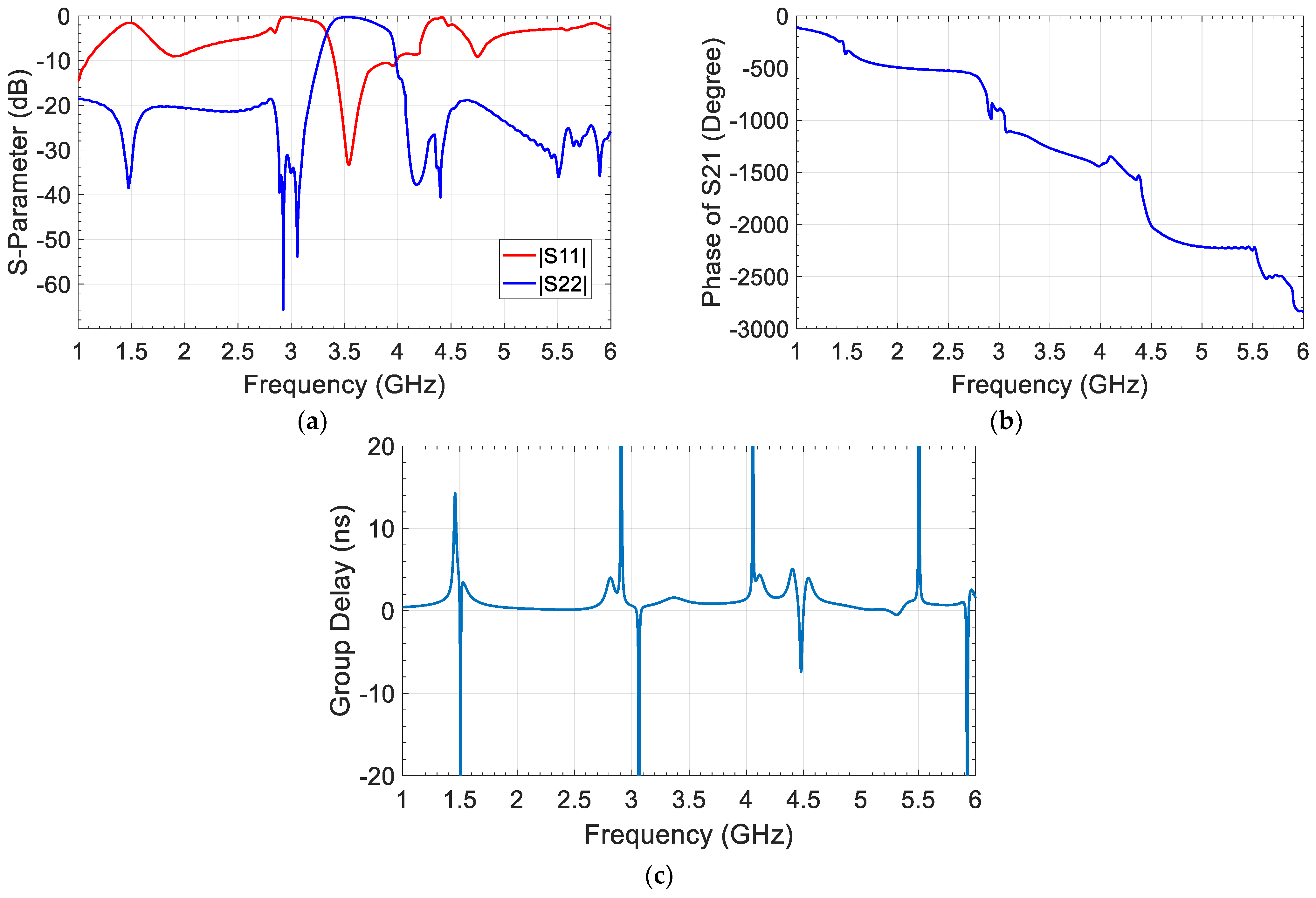
The reflection and transmission coefficients of the designed filter are simulated using CST microwave studio software 2023 and depicted in Figure 2a. The resulting transmission coefficient 3 dB bandwidth of the filter is equal to 0.54 GHz over the range 3.35–3.89 GHz, which represents the passband of the filter. This band perfectly covers the 5G mid-band applications (LTE 42 and LTE 43), which occupy the range 3.4–3.8 GHz. It is worth mentioning that the −10 dB reflection coefficient bandwidth is compatible with the 3 dB transmission coefficient bandwidth, as shown in the figure. The two transmission zeros adjacent to the passband have values equal to −53 dB (at 3.057 GHz) and −38 dB (at 4.171 GHz). Figure 2b illustrates the phase response of S21 of the proposed filter, where the proposed filter has an excellent linear phase within the passband. Figure 2c demonstrates the group delay of the proposed filter, which has a 0.72 ns in-band group delay variation ranging between 0.85 ns and 1.57 ns, which is very acceptable (within the passband) according to [31]. The following section demonstrates the design steps that were followed to obtain the final structure.
Figure 2.
Simulation results of the proposed filter: (a) magnitude of the scattering parameters, (b) phase response of S21, (c) group delay of the proposed filter.
3. Design Steps
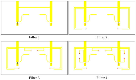
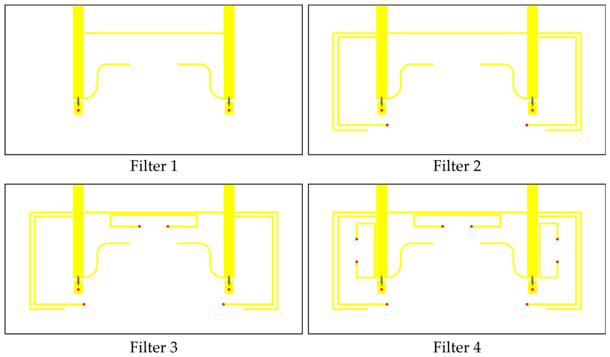
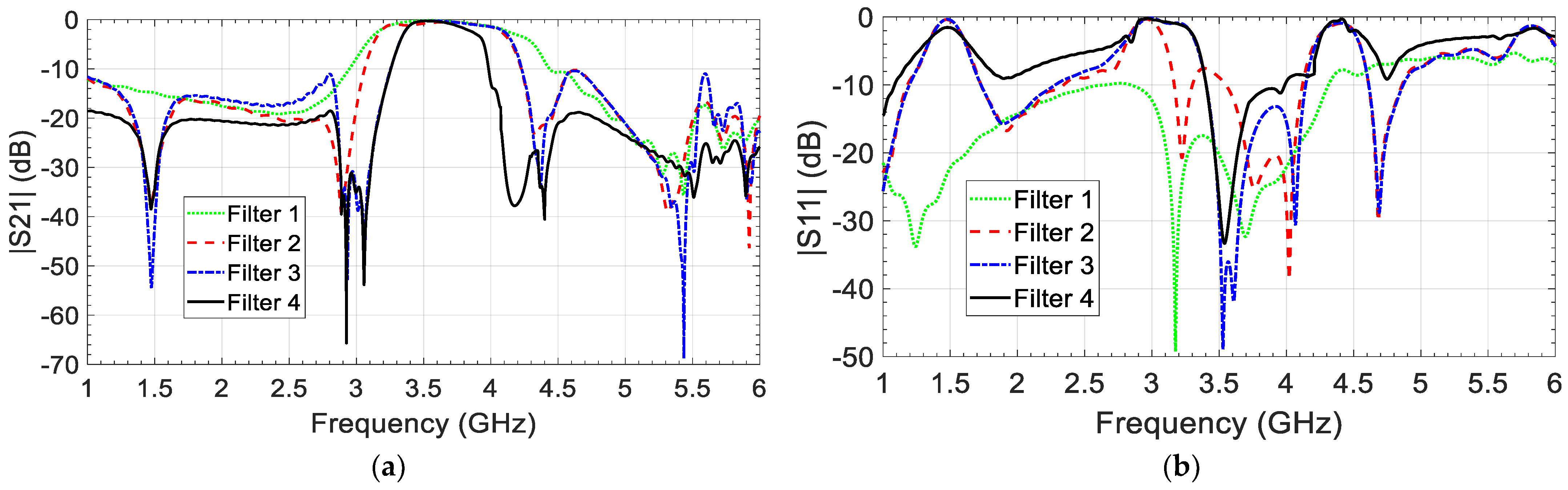
The steps that have been followed to reach the structure with the intended characteristics are illustrated in Figure 3 (Filters 1 to 4), while the magnitude of the reflection coefficient (|S11|) and the magnitude of the transmission coefficient (|S21|) are exhibited in Figure 4 with the aid of the CST Microwave Studio simulation suite. Filter 1 is the same starting point of the design that was proposed in [28]. It consists of a high-impedance BPF with a pair of band-stop filter elements (stubs) and a pair of resistive terminations. The resulting transmission coefficient has reasonable stop-band characteristics, but the 3 dB bandwidth is 1.046 GHz over the range (3.136–4.182) GHz, so it is much larger than the 5G mid-band, which extends over the range from 3.4 to 3.8 GHz. In addition, the transmission coefficient is not sharp enough to filter out the nearby undesired frequencies. Therefore, some modifications should be proposed for restricting the passband of the filter to hold the 5G mid-band with as narrow a transition band as possible while keeping the stop-band level as low as possible. This goal can be achieved by locating transmission zeros at certain frequencies to manipulate the stop-band and pass-band characteristics.
Figure 3.
The design procedure of the proposed filter.
Figure 4.
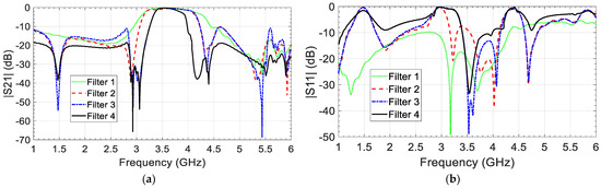
Simulation results of Filter 1–4: (a) transmission coefficient and (b) reflection coefficient.
In Filter 2, open- and short-circuit stubs are added to insert multiple transmission zeros into the transmission coefficient. The most effective zeros are those closer to 2.88 GHz and 4.32 GHz because they confine the passband to a value closer to that of the 5G mid-band with a sharper transition band than that of Filter 1. The 3 dB bandwidth is 0.936 GHz from 3.164 GHz to 4.1 GHz, but the reflection coefficient is still not acceptable within the passband. However, the stop-band characteristics are significantly improved around the passband.
In Filter 3, the first short-circuited U-shaped parasitic element is added as illustrated in Figure 3 to generate a transmission zero at 3.061 GHz. This zero improves the pass-band restriction by reducing the bandwidth to 0.773 GHz over the range (3.35–4.12) GHz. Although a single zero is added to the transmission coefficient, the performance of the filter is improved noticeably on the left-hand side of the passband.
In Filter 4, a pair of short-circuited U-shaped parasitic elements is added to introduce a transmission zero at 4.171 GHz. This makes the proposed filter more sensitive and sharper, as illustrated in Figure 4. The resulting 3 dB bandwidth of the transmission coefficient of the filter is equal to 0.54 GHz, from 3.35 GHz to 3.89 GHz. In addition, the −10 dB bandwidth of the reflection coefficient is compatible with the −3 dB transmission coefficient bandwidth (see Figure 4).
4. Filter Modeling and Mathematical Analysis
This section deals with the mathematical analysis and modeling of the proposed filter. As a result, it discusses each frequency modification mechanism separately in three different subsections.
4.1. Topology of One-Cell Filter
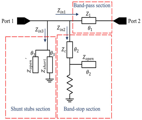
Figure 5 shows the topology of a one-cell BPF without the U-shaped parasitic elements. It consists of a band-pass section, a band-stop section, and two shunted open and short-circuited stubs. The input impedance of these sections can be derived from the well-known equation of the input impedance of the transmission lines [32]:
where Zin is the input impedance, Zo is the characteristic impedance of the transmission line, ZL is the load impedance, θ represents the electrical length of the transmission line , and 𝓁 denotes the length of the transmission line. The band-pass section is responsible for the band-pass characteristics of the filter, so it should satisfy the following conditions:
Figure 5.
Topology of a one-cell filter.
- When θ1 = 180°
- When θ1 = 90° & 270°
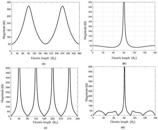
According to Equation (1), where λo is the wavelength of the resonant frequency, and Z1 should be as large as possible considering the fabrication limitations. Therefore, its value is selected to be equal to Z1 = 126.9 Ω. The variation of Zin1 is illustrated in Figure 6a, where it is equal to 50 Ω when θ1 = 180° and increases to a higher value (322 Ω) at θ1 = 90° & 270° to ensure matching in the central frequency and high impedance in the stop-band frequencies.
where
Figure 6.
Variation in the input impedance of: (a) band-pass section Zin1, (b) bandstop section Zin2, (c) shunt stub section Zin3, (d) Zin2 // Zin3.
The band-stop filter is responsible (with shunt stubs) for the band-stop characteristics of the filter, so it should satisfy the following condition by controlling the electrical lengths of the line and the open-circuited stub:
When θ2 = 90°
Thus, the lengths of the lines corresponding to Zc and Zopen are equal to , where Zc = 50 Ω, Zopen = 126.9 Ω [28]. Figure 6b illustrates the variation of Zin2 with θ2, where Zin2 = ∞ at the central frequency to maintain the passband unaffected.
Finally, the shunt stubs section can be analyzed as follows:
where , and .
As can be seen from Figure 6c, the input impedance of shunted stubs gives multiple zeros and multiple infinite impedance values. In this filter design, the length of these shunted stubs is selected to achieve an infinite impedance at the center frequency (fo = 3.6 GHz) and zero impedance around it [33].
where , and εre denotes the effective dielectric constant. Therefore:
∴ tan(2θ3) = ∞
∴𝓁 = 7.9288 or 23.78644 or 39.644083 or 55.5017……(mm)
The stubs’ length can take several values to locate an infinite input impedance at the center frequency of the pass-band, but there is a constraint on choosing the length value. As the length value increases, the zeros around the central frequency will be closer, which noticeably affects the pass-band characteristics of the filter because of the input impedance of the shunt stubs. Therefore, after some tests, the suitable value of the stubs length is selected to be equal to 𝓁 = 39.644 mm. Using the same concept, Zshort value should be large enough, and due to fabrication limitations Zshort = 126.9 Ω. Figure 6d declares the equivalent input impedance of the parallel of Zin2 & Zin3, which determines the general pass-band characteristics of the proposed filter. It contains a multi-zero impedance, which produces the transmission zeros of the filter and one infinity impedance at the central frequency, as mentioned earlier.
4.2. U-Shaped Parasitic Elements
The parasitic element is a piece of transmission line with short-circuit terminals whose characteristic impedance Zp1. The input impedance of this element is given by
where 𝓁 is the total length of the parasitic element. To make the transmission zero at fp1, then , such that tan β𝓁 = 0. This can be achieved when β𝓁 = π. Consequently, when applying the well-known formula:
One can deduce that when 𝓁 = 37.68 mm, the mathematical model gives a resonant frequency value of 3.0302 GHz, while in CST Studio Simulation Suite, the frequency is 3.061 GHz, which is very close to it, with a subtle difference equal to 30.8 MHz.
Similarly, the pair of U-shaped elements can be analyzed. When the total length is equal to 27.22 mm, the mathematical value of its resonant frequency is equal to 4.1938 GHz, while it is equal to 4.171 GHz using the CST studio suite. The difference between the two values is equal to 23 MHz, which is also very trivial compared to the filter frequency band of interest.
4.3. Current Distribution
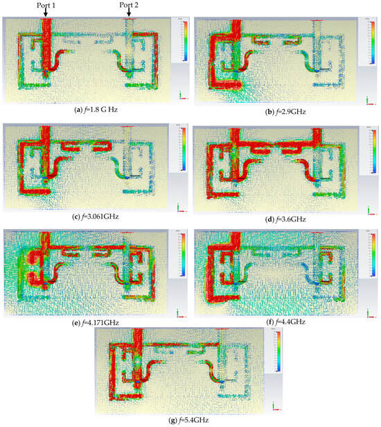
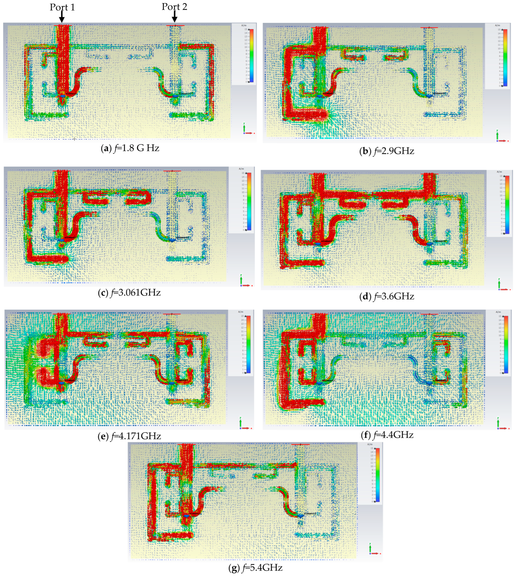
In this section, some frequencies are chosen to highlight the operation mechanism of the proposed filter, and Figure 7 shows the current distribution at different frequencies.
Figure 7.
Current distribution of the proposed filter when the signal is applied to port 1 of the filter at seven different frequencies (Note: the color-bar has minimum value equal to 0 and maximum value equal to 19).
The U-shaped element is a half-wavelength resonator, as explained mathematically previously in this section. In other words, when the current distributes in such a way that it is maximum at the shortest terminals and zero at the middle point of the element, the element stores the energy in the form of a standing wave. For this reason, the energy is confined within the U-shaped slot rather than transferring toward the second port, and the frequency that satisfies this condition is a frequency of a transmission zero. The same discussion can be generalized for the open-circuited stubs, but the current is distributed within the stub with zero values at the terminals and a maximum value at the middle point of the stub. On the other hand, the short-circuited stub is a quarter-wavelength resonator, so the current is maximum at the short-circuited terminal and zero at the other terminal of the stub. The frequency that corresponds to this distribution should be a frequency of a transmission zero.
As can be seen in Figure 7a, the current from port 1 is dissipated in the band-stop section at 1.8 GHz because the input impedance of the band-stop section is small compared to the high input impedance of the band-pass section. In Figure 7b, the current of port1 is concentrated in the shunt stubs section at 2.9 GHz because of the transmission zero that is added by the shunt stubs. At 3.061 GHz, Figure 7c reveals that the excitation current at port 1 is concentrated around the central U-shaped parasitic element that makes a transmission zero at this frequency and also in the parallel band-stop shunted stubs because they generate closely separated transmission zeros. Figure 7d shows the current distribution at the center frequency of the proposed filter (3.6 GHz). The current exciting port1 passes through the band-pass section to port 2 since all the band sections are designed to have open-circuit characteristics at this frequency.
In Figure 7e, the current at port 1 is stored within the pair of the U-shaped parasitic element because of the transmission zero that is added at this frequency. However, there is no current that reaches port2 because of the presented transmission zero. Figure 7f shows the effect of the transmission zero at 4.4 GHz caused by the shunt stub section. In addition, some current is dissipated in the second U-shaped parasitic element because it adds a transmission zero close to that of the shunt stubs. Finally, the excitation current is restricted around the shunted stub section at 5.4 GHz, as shown in Figure 7g. This is because of the high impedance of the band-pass section.
5. Parametric Study
To obtain the best filter response, a parametric study was applied to three parameters. These parameters are the total length of the central U-shaped parasitic element (Lu1), the total length of the pair of U-shaped parasitic elements (Lu2), and the total length of the shunted stubs (Lshunt). They are chosen because of their direct impact on the overall filter response. In addition, they contribute to generating transmission zeros that significantly improve the stop-band suppression and the transition band sharpness.
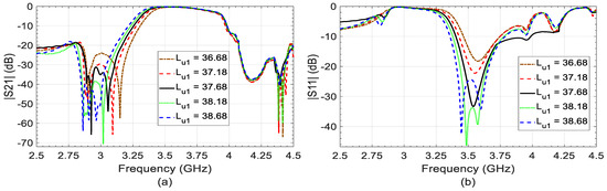
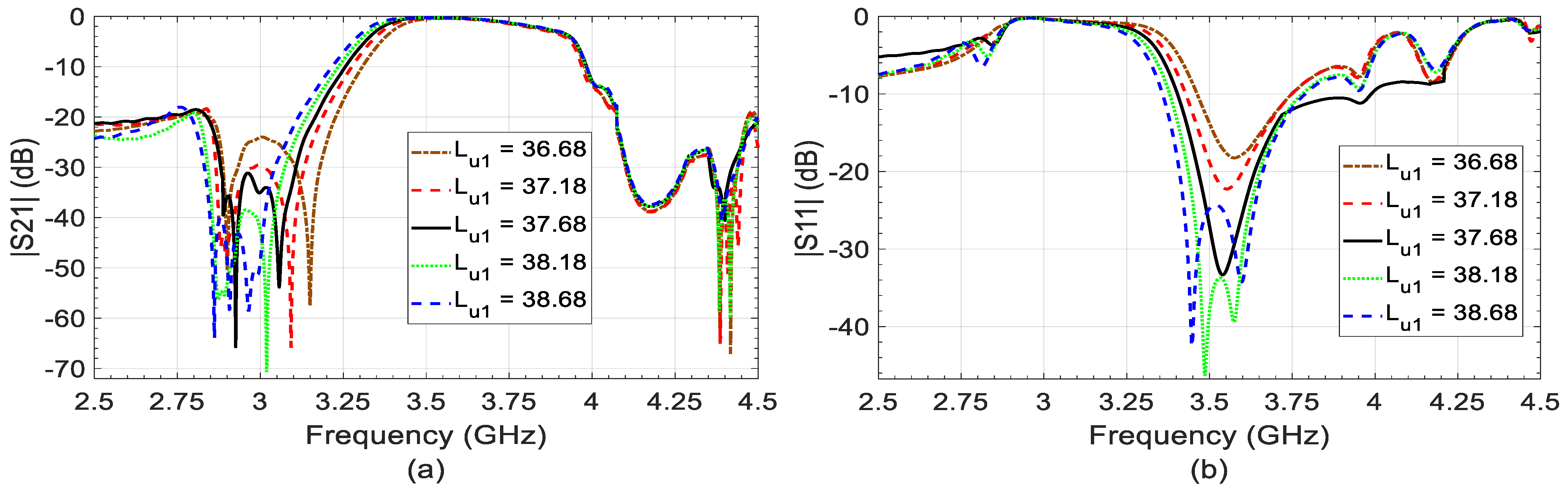
The first parameter is the total length of the central U-shaped parasitic element (Lu1), which is changed from 36.68 mm to 38.68 mm. It modifies the position of the transmission zero to the left side of the passband. This parameter provides precise control over the lower cut-off frequency, as illustrated in Figure 8a,b. It is easy to choose Lu1 that makes the lower cut-off frequency exactly at 3.4 GHz, but this causes a mismatch in the reflection coefficient of the filter. Therefore, the best value of Lu1 is 37.68 mm, which is almost equal to half the wavelength at the frequency of the transmission zero, as discussed in the previous section. Through the variation of Lu1 the passband was perturbed by ±58 MHz, the central frequency was shifted by ±28 MHz, and the insertion loss was varied by ±0.27 dB.
Figure 8.
Scattering parameters of the proposed filter at Lu2 = 27.22 mm, Lshunt = 39.644 mm, and different values of Lu1 (a) transmission coefficient and (b) reflection coefficient.
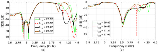
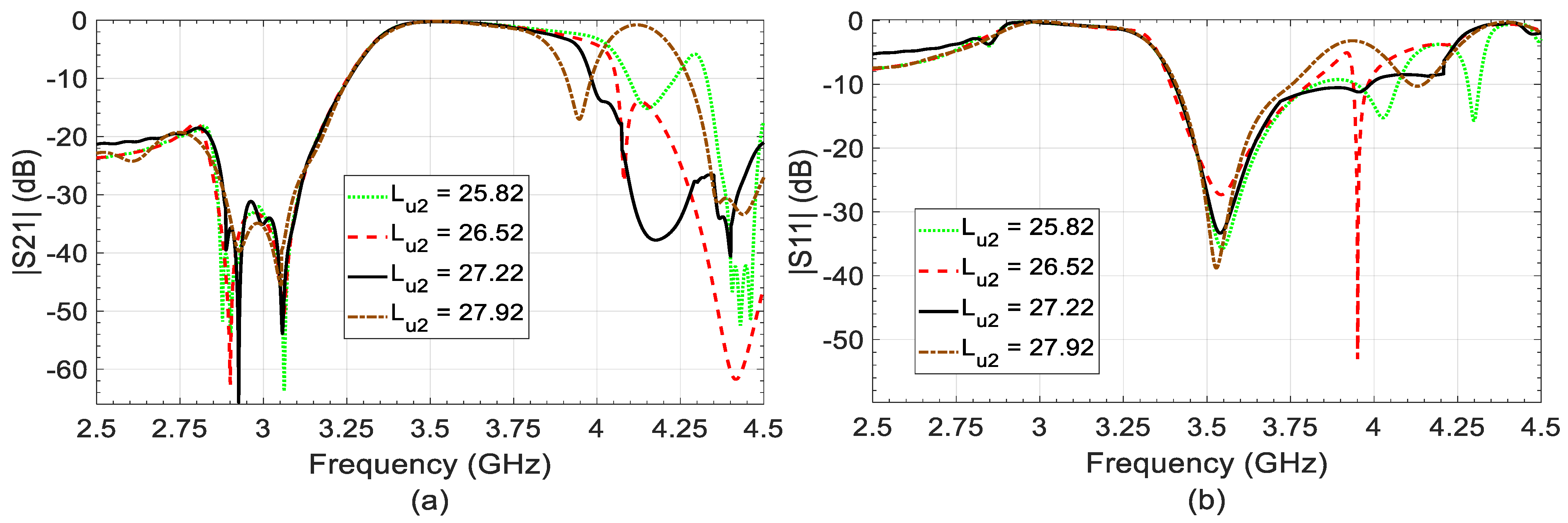
The second parameter is the total length of the pair of the U-shaped parasitic elements (Lu2), which is changed from 25.82 mm to 27.92 mm. It is such a critical parameter that it can add a second undesired pass-band beside the original one, as illustrated in Figure 9a,b. Therefore, to avoid this critical case, Lu2 should be chosen to make the transmission zero to the right of the pass-band close to the transmission zero that is produced by the shunted stubs. Consequently, the best value of Lu2 is 27.22 mm. Through the variation of Lu2, the passband was perturbed by ±100 MHz, the central frequency was shifted by ±61 MHz, and the insertion loss was varied by ±0.28 dB.
Figure 9.
Scattering parameters of the proposed filter at Lu1 = 37.68 mm, Lshunt = 39.644 mm, and different values of Lu1 (a) transmission coefficient and (b) reflection coefficient.
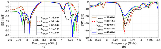
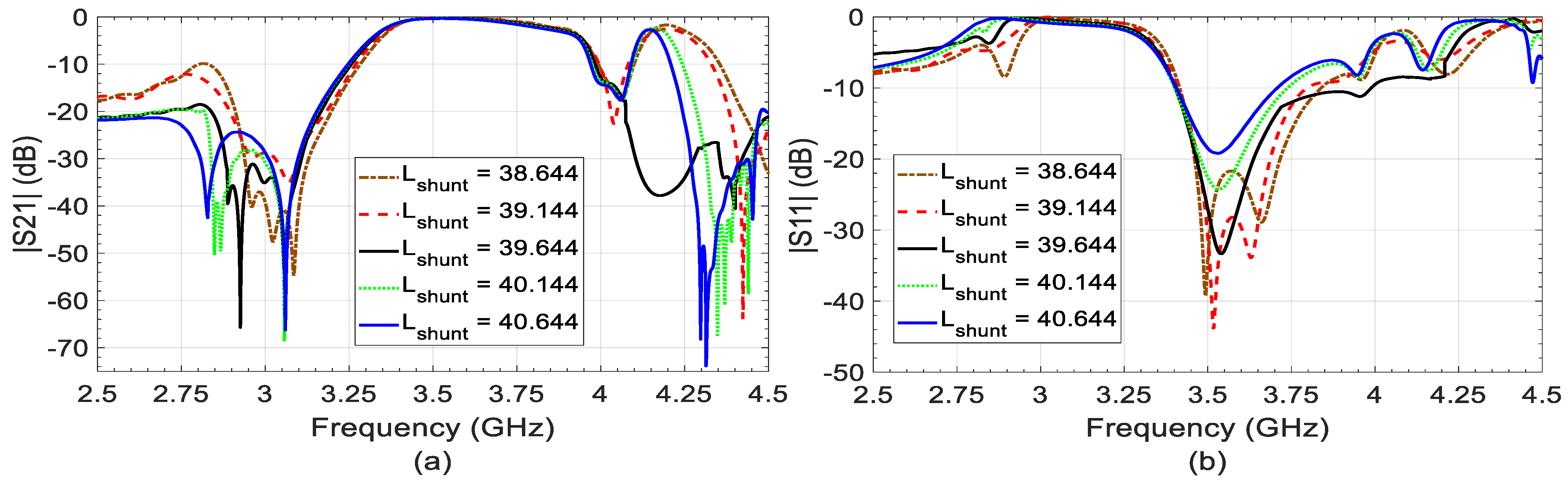
The third parameter is the total length of the shunted stubs Lshunt, which is changed from 38.644 mm to 40.644 mm. As revealed clearly in Figure 10, the position of the transmission zeros that are produced by the shunted stubs was shifted, and it affects both sides of the pass-band. As happened when Lu2 was changed, an undesired pass-band appears when the transmission zero position is changed on the upper side of the pass-band. Consequently, the best value of Lshunt is found to be equal to 39.644 mm. Through the variation in Lshunt, the passband was perturbed by ±65 MHz, the central frequency was shifted by ±60 MHz, and the insertion loss was varied by ±0.202 dB.
Figure 10.
Scattering parameters of the proposed filter at Lu1 = 37.68 mm, Lu2 = 27.22 mm, and different values of Lshunt (a) transmission coefficient and (b) reflection coefficient.
6. Measured Results
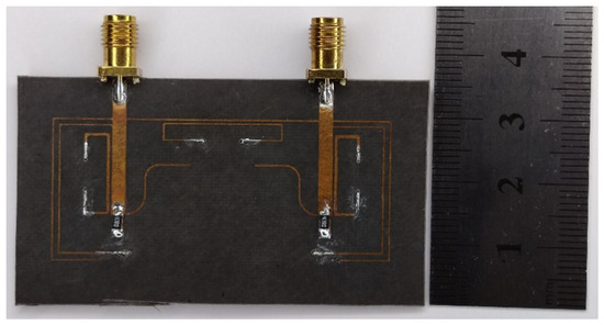
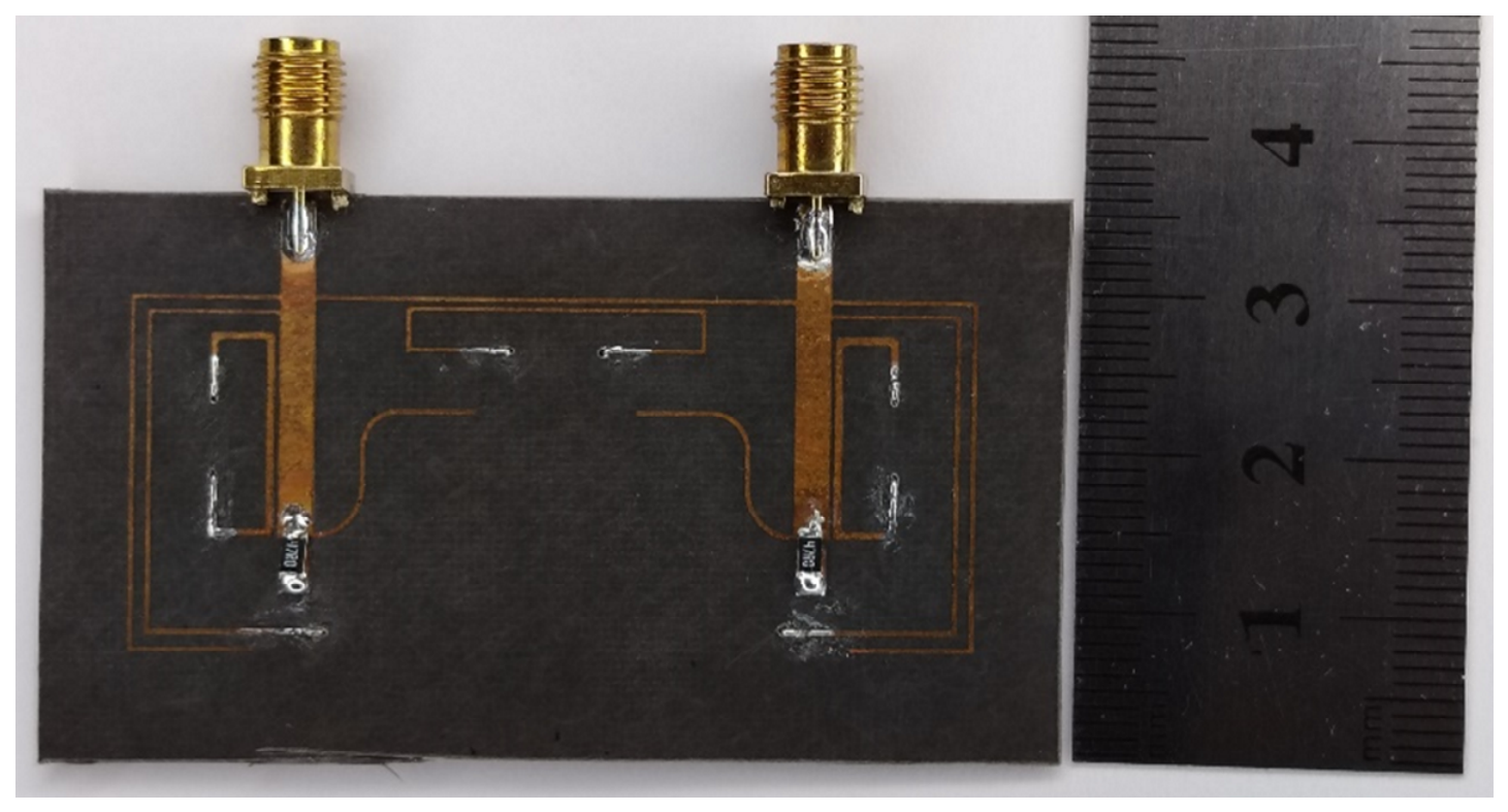
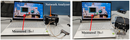
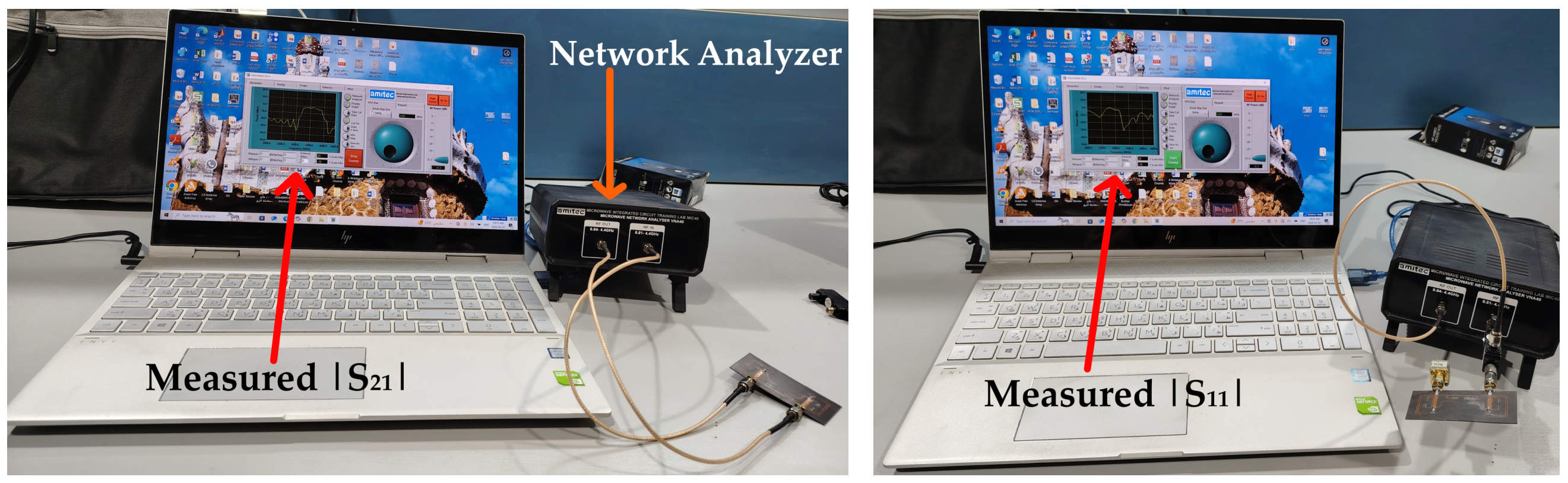
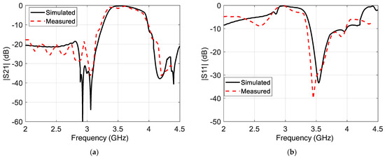
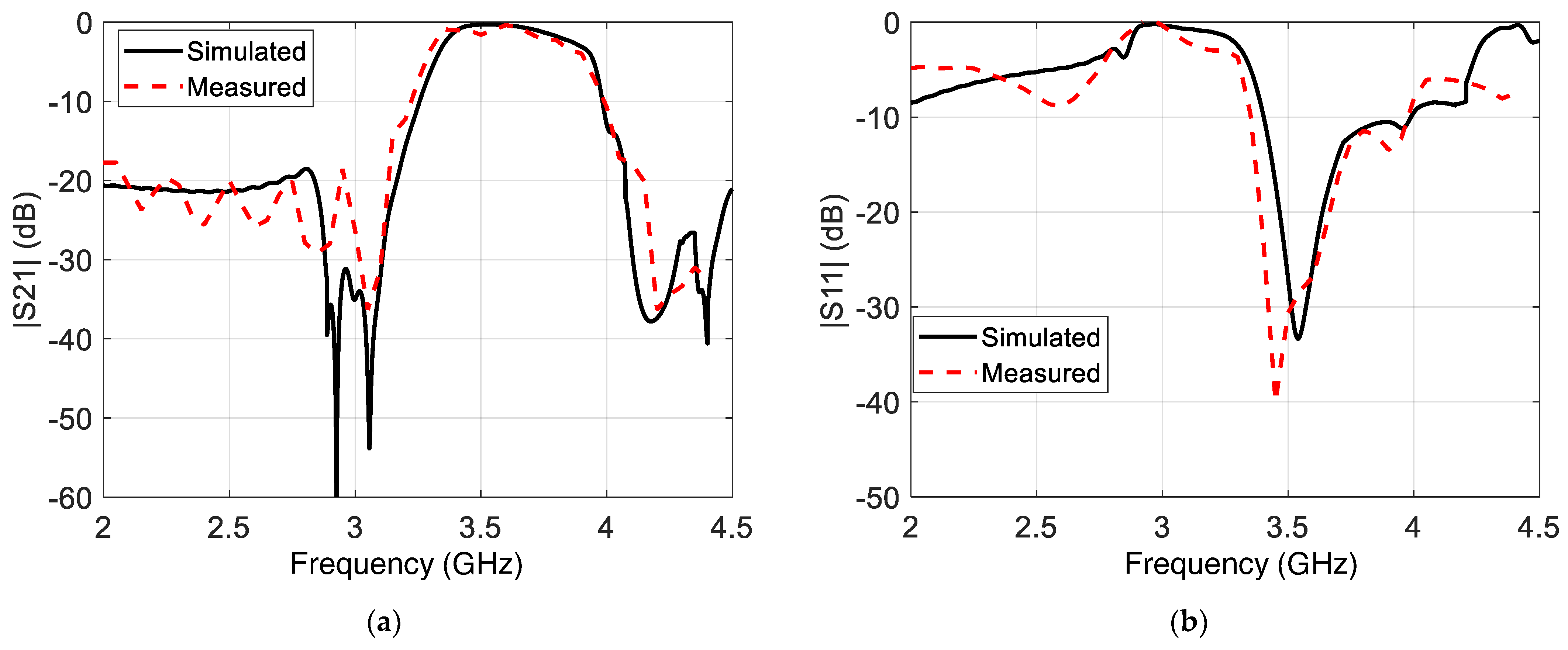
The fabricated version of the proposed filter is exhibited in Figure 11. The measurement outcomes are acquired using the AMITEC network analyzer shown in Figure 12. In Figure 13, the measured results are compared with the simulation results, and it is found that the measured −3 dB bandwidth is 0.52066 GHz from 3.30884 to 3.8295 GHz, whereas the simulation bandwidth is 0.54 GHz from 3.35 to 3.89 GHz. Consequently, there is good agreement between simulation and measured results, and the small deviation is caused by the imperfect manufacturing process and imperfect soldering. The proposed filter gives a very sharp response because of the four transmission zeros surrounding the passband, which makes the filter have an excellent lower and upper transition band equal to 7.1% and 10.2%, respectively, with respect to the central frequency. According to the references [34,35], the filter is said to be sharp when the transition band is within 10% and the stop-band attenuation is larger than 15 dB. Moreover, the measured stopband has a high stopband level attenuation approaching 20 dB. Table 1 presents a comparison with some other important designs to highlight the high performance of the proposed filter. All data in the table are measurements, not simulation values. FBW represents the fractional bandwidth with respect to fo. LTB is the lower transition band with respect to fo. UTB is the upper transition band with respect to fo. IL is the insertion loss. RL is the return loss. NTZ is the number of transmission zeros. TZ level represents the levels of the two transmission zeros adjacent to the passband.
Figure 11.
The prototype of the proposed band-pass filter.
Figure 12.
The measurement environment for the proposed filter.
Figure 13.
The simulation and measured S-parameters of the proposed filter: (a) transmission coefficient and (b) reflection coefficient.
Table 1.
Performance comparison with some other designs.
It is worthwhile mentioning that the discrepancy between the simulation and measured results comes from many factors. The fabrication tolerance is one of the most important factors since it may result in inaccurate dimensions for each filter component. The SMA connector is manually soldered, so this imperfect soldering also leads to undesired dispersion in the input current. Furthermore, the irregular variation in the value of the dielectric constant over the frequency is also an important factor that affects the measurement accuracy. Furthermore, the soldering of the short vias also directly affects the precision of the measured results.
Since the dielectric loss of the Rogers 5880 material is subtle, the power handling of the dielectric material is very high. However, the presence of the 50 Ω resistors has limited the power handling of the entire filter to the rated values of their manufacturing limitation. Therefore, the power handling of this filter is reduced to about 1 W, which is good enough for portable gadgets.
7. Conclusions
A sharp band-pass filter with enhanced passband and stop-band characteristics has been successfully designed and fabricated in this paper. The proposed filter perfectly covers the 5G mid-band with a measured fractional bandwidth of 14.44%. The two ports of the filter are terminated by 50 Ω resistors and connected by a high-impedance transmission line to form the passband section of the filter. This section results in a measured pass-band insertion loss equal to 0.35 dB at the resonant frequency of the filter. The pair of shunt short- and open-circuit stubs, the pair of short-circuited U-shaped parasitic elements, and the central short-circuited U-shaped element successfully improve the stop-band characteristics. The measured stop-band attenuation of the filter is found to be equal to 20 dB, while the transition band is within 10% (with respect to the center frequency) for the upper and the lower edges of the passband.
Author Contributions
Conceptualization, A.H.A. and F.M.A.; methodology, A.H.A.; investigation, A.H.A. and F.M.A.; resources, A.H.A., F.M.A. and Y.I.A.A.-Y.; writing—original draft preparation, A.H.A. and F.M.A.; writing—review and editing, A.H.A., F.M.A. and Y.I.A.A.-Y.; visualization, A.H.A., F.M.A., and Y.I.A.A.-Y. All authors have read and agreed to the published version of the manuscript.
Funding
This research received no external funding.
Data Availability Statement
The original contributions presented in this study are included in the article. Further inquiries can be directed to the corresponding author.
Conflicts of Interest
The authors declare no conflict of interest.
Abbreviations
The following abbreviations are used in this manuscript:
| ASIR | Asymmetrical Stepped Impedance Resonator |
| BPF | Band-pass Filter |
| BSF | Band-stop Filter |
| BW | Bandwidth |
| CPPN | Compositional Pattern Produce Network |
| DQN | Deep Q-Network |
| DSIR | Defected Stepped Impedance Resonator |
| FASOLR | Folded-Arms Square Open-Loop Resonator |
| FBW | Fractional Bandwidth |
| fo | Center Frequency |
| HMSIRC | Half-Mode Substrate Integrated Rectangular Cavity |
| HPF | High-Pass Filter |
| IL | Insertion Loss |
| LPF | Low Pass Filter |
| LTB | Lower Transition Band |
| MMR | Multiple Mode Resonator |
| MSIR | Microstrip Stepped Impedance Resonator |
| NTZ | Number of Transmission Zeros |
| QMR | Quintuple Mode Resonator |
| RL | Return Loss |
| SIDGS | Substrate Integrated Defected Ground Structure |
| SIW | Substrate Integrated Waveguide |
| SL-MMR | Stub Loaded Multiple Mode Resonator |
| SSS | Suspended Substrate Stripline |
| TZ | Transmission Zero |
| UTB | Upper Transition Band |
| UWB | Ultra-Wide Band |
References
- Pozar, D.M. Microwave Engineering, 4th ed.; John Wiley & Sons, Inc.: Hoboken, NJ, USA, 2012. [Google Scholar]
- Revathi, G.; Robinson, S. Design and Implementation of Highly Selective and Compact Low Profile Bandpass Filter for 5G Mid-Band Frequency Applications. Wirel. Pers. Commun. 2023, 130, 363–375. [Google Scholar] [CrossRef] [Scilit]
- Al-Yasir, Y.I.A.; Parchin, N.O.; Alabdallah, A.; Abdulkhaleq, A.M.; Sajedin, M.; Elfergani, I.T.E.; Abd-Alhameed, R.A. Design, Simulation and Implementation of Very Compact Open-Loop Trisection BPF for 5G Communications. In Proceedings of the 2019 IEEE 2nd 5G World Forum (5GWF), Dresden, Germany, 30 September–2 October 2019; IEEE: New York, NY, USA, 2019; pp. 189–193. [Google Scholar]
- Alnahwi, F.M.; Al-Yasir, Y.I.A.; Abdulhameed, A.A.; Abdullah, A.S.; Abd-Alhameed, R.A. A Low-Cost Microwave Filter with Improved Passband and Stopband Characteristics Using Stub Loaded Multiple Mode Resonator for 5G Mid-Band Applications. Electronics 2021, 10, 450. [Google Scholar] [CrossRef] [Scilit]
- Barik, R.K.; Koziel, S.; Pietrenko-Dabrowska, A. Broad Stopband, Low-Loss, and Ultra-Compact Dual-Mode Bandpass Filter Based on HMSIRC. Electronics 2023, 12, 2831. [Google Scholar] [CrossRef] [Scilit]
- Fan, C.; Ma, S.; Gong, K.; Sun, J.; Qian, H.; Liu, Q.; Liu, Y. Highly Selective Microstrip Bandpass Filters Using Dual-Mode Patch Resonator Loaded with Short Via. AEU Int. J. Electron. Commun. 2024, 185, 155457. [Google Scholar] [CrossRef] [Scilit]
- Al-Yasir, Y.I.A.; Tu, Y.; Bakr, M.S.; Parchin, N.O.; Asharaa, A.S.; Mshwat, W.A.; Abd-Alhameed, R.A.; Noras, J.M. Design of Multi-standard Single/Tri/Quint-wideband Asymmetric Stepped-impedance Resonator Filters with Adjustable TZs. IET Microw. Antennas Propag. 2019, 13, 1637–1645. [Google Scholar] [CrossRef] [Scilit]
- Nwajana, A.O.; Obi, E.R. Application of Compact Folded-Arms Square Open-Loop Resonator to Bandpass Filter Design. Micromachines 2023, 14, 320. [Google Scholar] [CrossRef] [Scilit] [PubMed]
- Kahkesh, S.H.; Sheikhi, A. A Microstrip Bandpass Filter Using Coupled Lines Loaded by Open Stubs. Sci. Rep. 2024, 14, 26680. [Google Scholar] [CrossRef] [Scilit] [PubMed]
- Wójcik, D.; Surma, M.; Magnuski, M. Compact Microstrip Fixed-Frequency Double-Coupled Double-Tuned Filter with Selected Band Suppression. Sensors 2025, 25, 6768. [Google Scholar] [CrossRef] [Scilit] [PubMed]
- Cui, L.; Wu, W.; Shen, Z.; Fang, D. A Miniaturized Bandpass Filter with Low Passband Insertion Loss and High Harmonic Suppression in Ultra-Wide Stopband. Chin. J. Electron. 2012, 21, 173–178. [Google Scholar]
- Chen, X.; Li, Z.; Li, H.-L.; Xiong, Y.; Li, C.-P.; Li, D.; Qian, L.-R.; Wang, L.-T. Wideband Bandpass Filters with Ultrawide Stopband Based on Cascade Multiple Square Ring Elements. IEEE Microw. Wirel. Technol. Lett. 2025, 35, 1881–1884. [Google Scholar] [CrossRef] [Scilit]
- Chedurupalli, S.; Saripaka, L.; Thumiki, A.; James Raju, K.C. Highly Selective Compact Cascaded Suspended Stripline Bandpass Filter. IEEE Microw. Wirel. Technol. Lett. 2025, 35, 1276–1279. [Google Scholar] [CrossRef] [Scilit]
- Hasan, Y.M.; Abdullah, A.S.; Alnahwi, F.M. Compact Low-Cost Reconfigurable Microwave Bandpass Filter Using Stub-Loaded Multiple Mode Resonator for WiMAX, 5G and WLAN Applications. Basrah J. Eng. Sci. 2022, 22, 78–85. [Google Scholar] [CrossRef] [Scilit]
- Alnahwi, F.M.; Abdulhameed, A.A.; Ali, N.T.; Al-Yasir, Y.I.A.; Kubík, Z.; Abdullah, A.S.; Abd-Alhameed, R.A. A Compact Filtering Antenna with Step and Continuous Tuning Modes for WiMAX Cognitive Radio Communication. IEEE Access 2023, 11, 135394–135405. [Google Scholar] [CrossRef] [Scilit]
- Rajender, R.; Barik, R.K.; Ciarpi, G.; Koziel, S.; Genovesi, S.; Rossi, D. A Novel Multi-Mode Resonator-Based Ultra-Wideband Bandpass Filter Topology. Electronics 2025, 14, 3992. [Google Scholar] [CrossRef] [Scilit]
- Sazid, M.; Agrawal, N.; Gautam, A.K.; Nagar, M.R. Miniaturized RF Reconfigurable Bandpass Filter with Dynamic Wideband Frequency and Constant Bandwidth Tuning Capability. Sci. Rep. 2026, 16, 7858. [Google Scholar] [CrossRef] [Scilit] [PubMed]
- Wu, B.; Liang, C.-H.; Li, Q.; Qin, P.-Y. Novel Dual-Band Filter Incorporating Defected SIR and Microstrip SIR. IEEE Microw. Wirel. Compon. Lett. 2008, 18, 392–394. [Google Scholar] [CrossRef] [Scilit]
- Liang, G.-Z.; Chen, F.-C. A Compact Dual-Wideband Bandpass Filter Based on Open-/Short-Circuited Stubs. IEEE Access 2020, 8, 20488–20492. [Google Scholar] [CrossRef] [Scilit]
- Tang, D.; Han, C.; Deng, Z.; Qian, H.J.; Luo, X. Substrate-Integrated Defected Ground Structure for Single- and Dual-Band Bandpass Filters with Wide Stopband and Low Radiation Loss. IEEE Trans. Microw. Theory Tech. 2021, 69, 659–670. [Google Scholar] [CrossRef] [Scilit]
- Shankar, E.; Phani Kumar, K.V.; Krishna Velidi, V.; Koziel, S. Miniaturized Dual-Band Bandpass Filter with Wide Inter Stopband for 5G Applications. IEEE Trans. Circuits Syst. II Express Briefs 2024, 71, 4461–4465. [Google Scholar] [CrossRef] [Scilit]
- Iqbal, A.; Ahmad, A.W.; Smida, A.; Mallat, N.K. Tunable SIW Bandpass Filters with Improved Upper Stopband Performance. IEEE Trans. Circuits Syst. II Express Briefs 2020, 67, 1194–1198. [Google Scholar] [CrossRef] [Scilit]
- Li, Q.; Yang, T. Compact UWB Half-Mode SIW Bandpass Filter with Fully Reconfigurable Single and Dual Notched Bands. IEEE Trans. Microw. Theory Tech. 2021, 69, 65–74. [Google Scholar] [CrossRef] [Scilit]
- Pradhan, N.C.; Koziel, S.; Barik, R.K.; Pietrenko-Dabrowska, A. Bandwidth-Controllable Third-Order Band Pass Filter Using Substrate-Integrated Full- and Semi-Circular Cavities. Sensors 2023, 23, 6162. [Google Scholar] [CrossRef] [Scilit] [PubMed]
- Máximo-Gutiérrez, C.; Hinojosa, J.; Alvarez-Melcon, A. A Technique for the Passband and Stopband Control of Wideband Band-Pass Substrate Integrated Waveguide (SIW) Filters Designed with Elliptic Stepped Impedances. AEU Int. J. Electron. Commun. 2024, 177, 155172. [Google Scholar] [CrossRef] [Scilit]
- Magnuski, M.; Noga, A.; Surma, M.; Wójcik, D. Modified Triple-Tuned Bandpass Filter with Two Concurrently Tuned Transmission Zeros. Sensors 2022, 22, 9760. [Google Scholar] [CrossRef] [Scilit] [PubMed]
- Lu, X.; Fang, X.; Kong, Q.; Zhang, R.; Zhou, S.; Zhou, L.; Luo, X.; Yang, Y.; Liu, Q. Miniature Wideband Superconducting Filter Design with Four Transmission Zeros Based on Quintuple-Mode Resonator (QMR). IEEE Microw. Wirel. Technol. Lett. 2025, 35, 1486–1489. [Google Scholar] [CrossRef] [Scilit]
- Luo, C.; Wong, S.-W.; Lin, J.-Y.; Yang, Y.; Li, Y.; Yu, X.-Z.; Feng, L.-P.; Tu, Z.-H.; Zhu, L. Quasi-Reflectionless Microstrip Bandpass Filters Using Bandstop Filter for Out-of-Band Improvement. IEEE Trans. Circuits Syst. II Express Briefs 2020, 67, 1849–1853. [Google Scholar] [CrossRef] [Scilit]
- Cho, Y.-H.; Park, C. Deep Reinforcement Learning-Based Adaptive Bandpass Filter with Reconfigurable Frequency and Bandwidth. IEEE Microw. Wirel. Technol. Lett. 2025, 35, 1700–1703. [Google Scholar] [CrossRef] [Scilit]
- Wang, H.; Nie, C.; Ren, Z.; Li, Y. A Generative Model-Based Method for Inverse Design of Microstrip Filters. Electronics 2025, 14, 1989. [Google Scholar] [CrossRef] [Scilit]
- Yang, K.; Su, M.; Chen, P. Design of Dualband Bandpass High-Temperature Superconducting Filter with Group Delay Equalization. IEEE Access 2021, 9, 149925–149933. [Google Scholar] [CrossRef] [Scilit]
- Liao, S.Y. Microwave Devices and Circuits, 2nd ed.; Prentice-Hall: Englewood Cliffs, NJ, USA, 1985. [Google Scholar]
- Garg, R.; Bahl, I.J. Microstrip Lines and Slotlines, 4th ed.; Artech House: Boston, MA, USA; London, UK, 2025. [Google Scholar]
- Karimi, G.; Lalbakhsh, A.; Siahkamari, H. Design of Sharp Roll-Off Lowpass Filter with Ultra Wide Stopband. IEEE Microw. Wirel. Compon. Lett. 2013, 23, 303–305. [Google Scholar] [CrossRef] [Scilit]
- Ai, J.; Zhang, Y.H.; Xu, K.D.; Shen, M.K.; Joines, W.T. Miniaturized Frequency Controllable Band-Stop Filter Using Coupled-Line Stub-Loaded Shorted SIR for Tri-Band Application. IEEE Microw. Wirel. Compon. Lett. 2017, 27, 627–629. [Google Scholar] [CrossRef] [Scilit]

Disclaimer/Publisher’s Note: The statements, opinions and data contained in all publications are solely those of the individual author(s) and contributor(s) and not of MDPI and/or the editor(s). MDPI and/or the editor(s) disclaim responsibility for any injury to people or property resulting from any ideas, methods, instructions or products referred to in the content. |
© 2026 by the authors. Licensee MDPI, Basel, Switzerland. This article is an open access article distributed under the terms and conditions of the Creative Commons Attribution (CC BY) license.