


Abstract
This paper is dedicated to the determination of the electrical properties of a wire arc additively manufactured (WAAM) aluminum alloy component. Statistical processing of the electrical properties and hollow micro-interlayer zones of the WAAM sample made of ER4043 aluminum alloy is performed. The eddy current electrical conductivity measurement method is employed for WAAM 3D-printed sample surface properties mapping. Measured data on electrical conductivity are estimated depending on the 3D printing axis directions and the lift-off distance from the sample surface. The 3D standard deviation is calculated for property anisotropy correlation. These data can be used for improved additive manufacturing control for enhanced electrical conductivity of aluminum WAAM samples as well as for numerical modeling of the properties of such samples.
1. Introduction
Wire Arc Additive Manufacturing (WAAM) is one of the fastest-developing technologies for metal 3D printing, showing fast deposition of large quantities of melted metal. Metal 3D printing is of general interest in electrical and electronic engineering because it enables the achievement of good electrical properties, such as electrical conductivity and magnetic permeability [1,2,3]. However, the high deposition speed of WAAM demonstrates a huge variation in the achieved properties, exhibiting significant anisotropy along the printing direction and normal to it [3,4,5]. These properties are mainly studied as mechanical properties [1,2] and thermal density deviations [3,4,5,6], but electrical parameters, such as electrical conductivity, are poorly investigated. One of the defining features of WAAM is the very high deposition rate [1,2,3], which distributes large quantities of material. In that process, the material goes through a phase transition as it melts, distributes, and cools. These stages exhibit variations in material density and internal structural anisotropy that are further reflected in macroscopic material properties from mechanical, electrical, and magnetic points of view. However, WAAM also has some drawbacks. The surface finish of the parts is relatively rough, requiring post-processing such as machining to achieve the desired precision. Dimensional accuracy is lower than that in powder-bed fusion processes, since the molten pool and heat input can cause distortion. Residual stresses and warping are common challenges, and porosity or cracking may occur if process parameters are not carefully controlled [6,7]. The method is best suited to medium-to-large, relatively simple geometries rather than highly intricate designs.
Statistical data processing can provide important information about the distribution range of non-primary material properties, such as electrical conductivity. This is not aluminum intrinsic conductivity, but the macroscale sample’s electrical conductivity, influenced by layer density, internal stress, alloy anisotropy, etc.
In this work, results of the statistical processing of the electrical properties of a WAAM ER4043 aluminum alloy component are presented. The eddy current electrical conductivity measurement method is employed for WAAM 3D-printed sample surface properties mapping. Measured electrical conductivity data are estimated depending on the 3D printing axis directions and the lift-off distance from the sample surface. Bi-directional standard deviation is calculated for property anisotropy correlation. These data can be used for improved additive manufacturing control for enhanced electrical conductivity of aluminum WAAM samples.
2. WAAM Sample Preparation
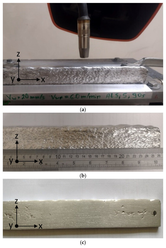
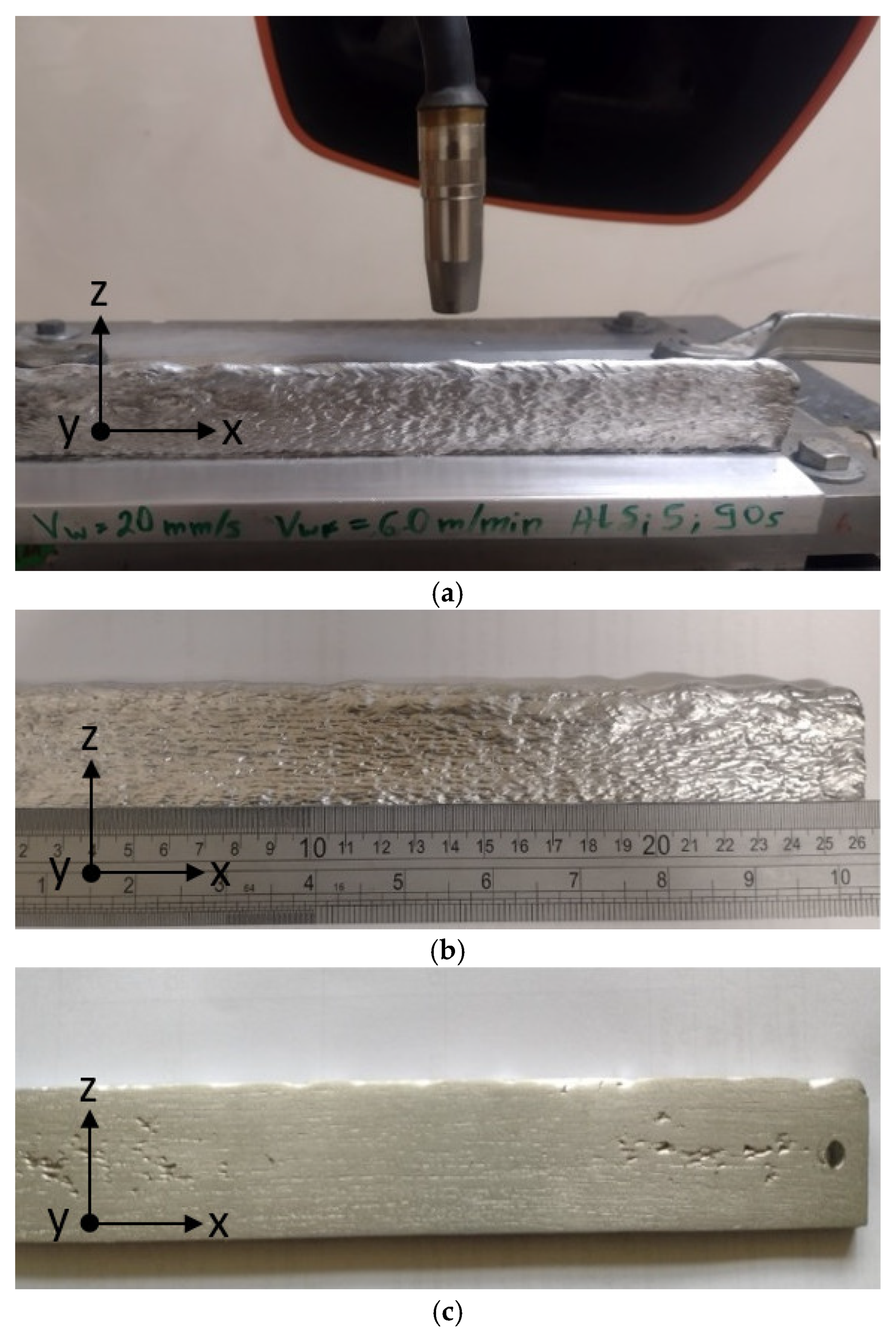
The wall-shaped component, shown in Figure 1a, was 3D-printed using a wire arc additive manufacturing setup comprising a KUKA KR 15/1 robotic arm, an EWM welding torch, an EWM wire feeder, and an EWM Alpha Q 552 puls welding unit. The welding wire had a diameter of 1.2 mm and a chemical composition as follows: 5% Si; 0.6% Fe; 0.3% Cu; 0.15% Mn; 0.2% Mg; 0.1% Zn; 0.0003% Be; 0.15% Ti; 0.15% others; balance Al. This chemical composition corresponds to the aluminum alloy ER4043. The substrate used for the deposition process was an ER6082-T6 aluminum alloy with the following chemical composition: 0.40–1.00% Mn; 0.5% Fe; 0.6–1.2% Mg; 0.7–1.3% Si; 0.10% Cu; 0.20% Zn; 0.10% Ti; 0.25% Cr; 0.20% others, balance Al. The process was carried out using a wire feeding speed of 6.0 m/min, a welding speed of 1.2 m/min, a current of 119 A, and a voltage of 17.4 V. Due to the low affinity of aluminum towards high temperatures, a wait time of 60 s was applied, which was enough not to overheat each consecutive layer. This time was applied after previous experiments showed improved accuracy and quality of deposition of the layers by increasing the wait time gradually to 60 s. During the process, Ar inert gas was used with a purity of 99.999% and a flow rate of 17 L/min. An offset of the welding torch perpendicular to the welding direction after each layer of 1.0 mm/layer was chosen. The specimen was built to a length of 300 mm, a height of 46 mm, and a thickness of 6 mm.
Figure 1.
As-built WAAM specimen (a), specimen cut to size (b), and tested ground specimen (c).
After the deposition process, the specimen was removed from the substrate, as shown in Figure 1b, and ground using a ceramic abrasive wheel. Following this process, the specimens were also ground using abrasive paper with P40 grit, P80 grit, P120 grit, and finally P240 grit. The ground component is shown in Figure 1c. Two openings with a diameter of 6 mm were made on each side of the specimen in order to secure it to the grinding base. The final dimensions of the specimen, after the grinding process, were 260 mm in length, 40 mm in height, and a thickness of 6 mm.
Tested properties were measured over a surface mesh with 50 × 3 × 5 local testing nodes in the corresponding x, y, and z directions on the 3D-printed aluminum sample. In this way, material properties surface mapping was performed. For the x and z directions testing an overlapping sensor locations were used. The resolution was increased to a 5 mm step size, which is smaller than the coil diameter, by overlapping sensor coil locations.
3. Eddy Current Conductivity Testing
Eddy current testing is a non-destructive testing (NDT) method that uses an alternating electromagnetic field to inspect conductive materials for internal inhomogeneities, such as flaws or cracks, to measure coating or material thickness, and to assess electrical and magnetic material properties. It is a volumetric method that gives a signal from the sample interior, but is limited by the penetration depth of eddy currents, which is frequency-dependent.
Eddy current conductivity testing is realized by an electric coil carrying an alternating current that generates a changing magnetic field. When placed near a conductive surface, such as aluminum, this field induces eddy currents in the material, which are detected by the primary coil or a special magnetic field sensor. The method is fast, accurate, local, contactless, and capable of detecting very small defects or material properties deviations.
The NORTEC N600C NDT (Olympus Co., Waltham, MA, USA) device is used in the electrical conductivity testing mode. Testing is performed with a Conductivity Mode Probe at a frequency of 60 kHz; the probe coil diameter is 20 mm, and the scanning step resolution is 5 mm at a 3D Cartesian coordinate system. It shows, for each testing location, the material electrical conductivity value and the lift-off distance, which is related to surface deviations below the testing coil. Measured data are recorded in IACS% units (International Annealed Copper Standard). IACS is a reference standard for electrical conductivity, using annealed copper as the benchmark. Conductivity is measured as a percentage of IACS, where 100% IACS represents the conductivity of annealed copper at 20 °C, which is 58 MS/m. A higher percentage of IACS indicates greater conductivity.
Tested properties are measured over a surface mesh 50 × 3 × 5 local testing nodes in the corresponding x, y, and z directions on the 3D-printed aluminum sample with a length of 300 mm, a thickness of 6 mm, and a height of 46 mm. The tested sample (Figure 1c) has two sides, denoted as the A side and the B side.
In order to estimate the homogeneity of the electrical conductivity of the sample, statistical processing of the measured properties is performed by evaluating the mean and standard deviation of the measured datasets.
where μ is the mean value of the given dataset Ai.
For the given measured dataset Ai, the standard deviation St is expressed as
where μ is the precalculated mean value from (1), and N is the number of samples in the given dataset.
When a 3D data matrix corresponding to measured mesh nodes is available, a composite standard distribution can be expressed as directional linear groups, with data lines along x, y, and z as subgroups.
The normal Gaussian distribution as a 3D density function Df is represented as (3)
where A is the 3D array of measured electrical conductivities or lift-off distances, which correspond to the measuring mesh nodes in the coordinate directions.
For the directional case considered, the density function is represented as 3D with degrees of freedom corresponding to the directions of the sample, where means (4) and standard deviations (5) are determined independently for each direction x, y, and z.
The means are structured in a vector matrix of size 3 × 1, Equation (4), and the covariance matrix size is 3 × 3, Equation (5).
4. Results
To estimate the homogeneity of the sample electrical conductivity distributions, eddy current testing was performed on the WAAM aluminum 3D-printed sample, as described methodologically above.
Tested properties were measured over a surface mesh with 50 × 3 × 5 local testing nodes in the corresponding x, y, and z directions on the 3D-printed aluminum sample. In this way, material properties surface mapping was performed. For the x and z directions, overlapping testing sensor locations were used. Resolution was increased by using a 5 mm step size, which is smaller than the coil diameter, through overlapping sensor coil locations. The tested sample (Figure 1c) has two sides, denoted as the A side and the B side.
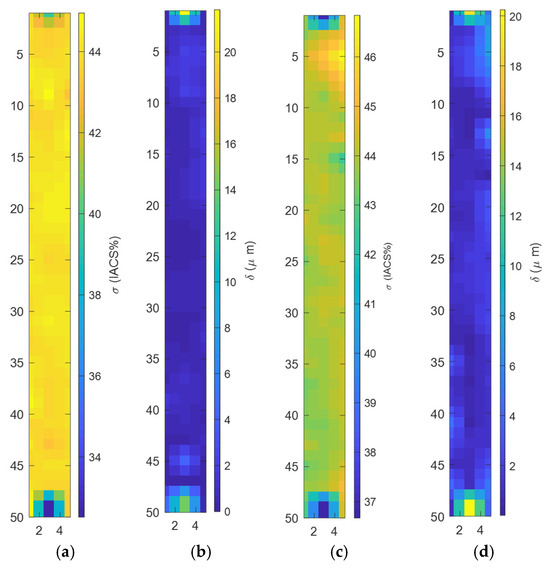
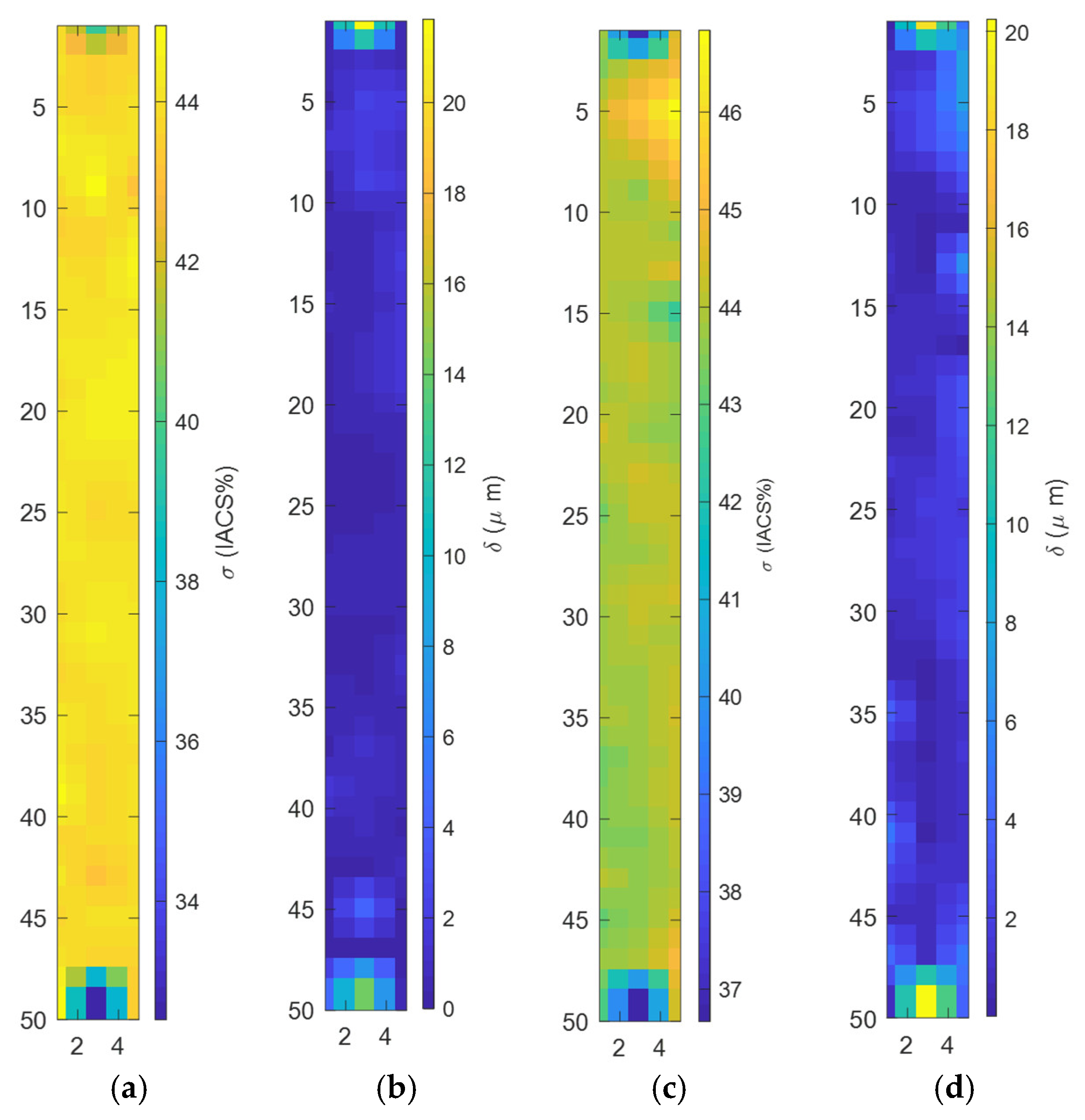
In order to estimate the homogeneity of the electrical conductivity distribution of the sample, statistical processing of the measured properties was performed by evaluating the mean and standard deviation of the measured datasets. The measured datasets are shown in Figure 2. They represent the two sides of the tested sample shown in Figure 1c. The measured electrical conductivity distribution of side A of the sample is presented in Figure 2a; the measured lift-off gap distance for side A is shown in Figure 2b; the measured electrical conductivity distribution of side B of the sample is shown in Figure 2c; and the measured lift-off gap distance for side B is shown in Figure 2d.
Figure 2.
Measured electrical conductivity distributions of the sample—side A (a), measured lift-off gap distance—side A (b), measured electrical conductivity distributions of the sample—side B (c), measured lift-off gap distance—side B (d).
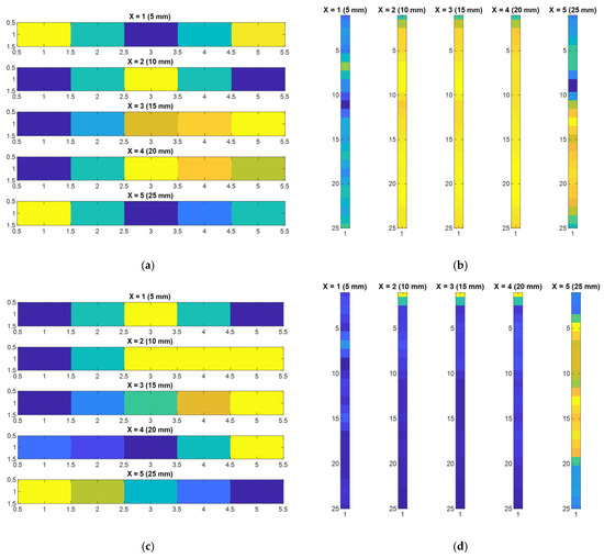
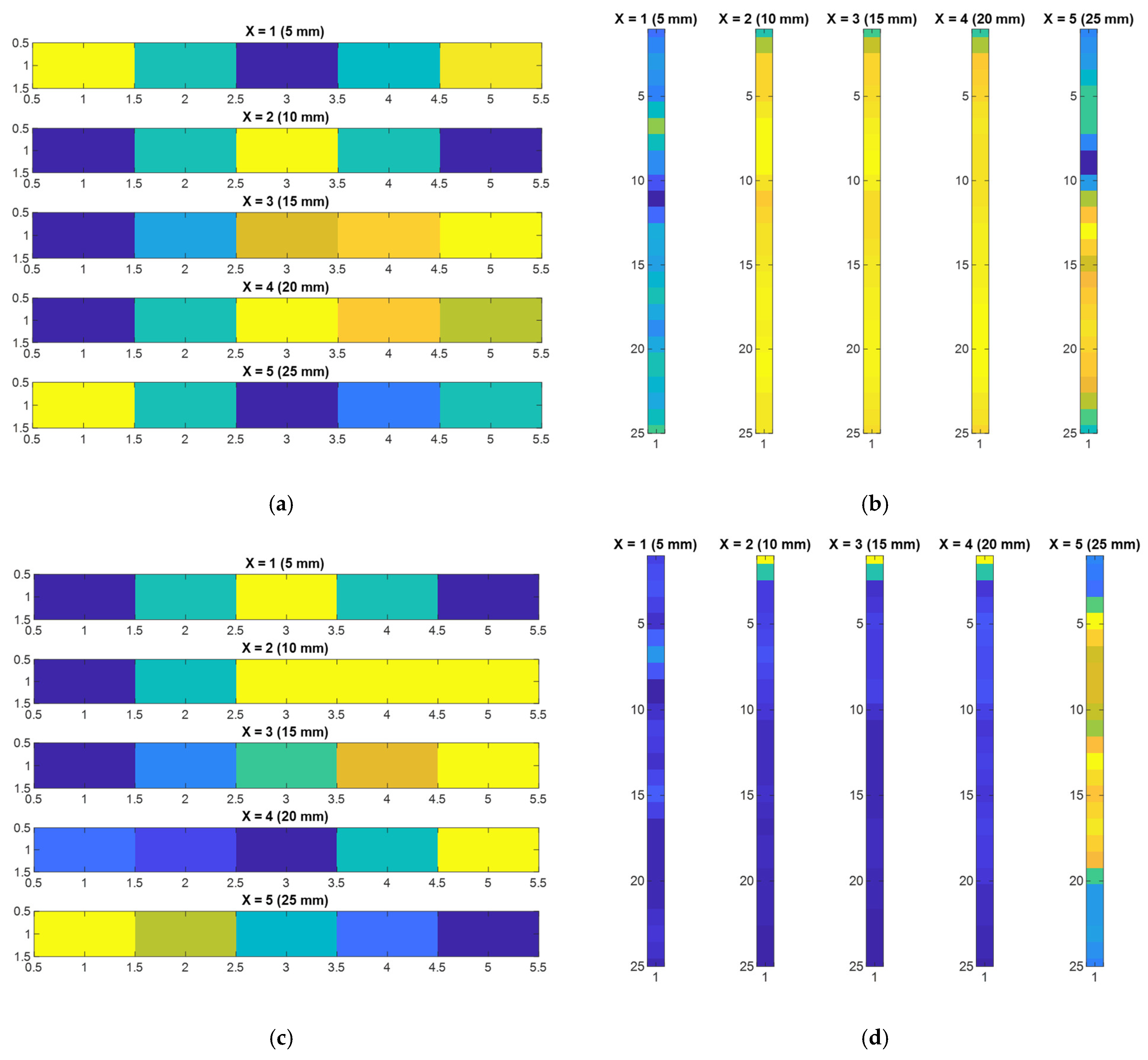
The measured electrical conductivity distribution of the sample by the main coordinate directions is presented as follows: measured electrical conductivity in the z direction for linear groups at side A is presented in Figure 3a, measured electrical conductivity in the x direction for linear groups at side A in Figure 3b, measured lift-off gap distance in the z direction for linear groups at side A is presented in Figure 3c, and measured lift-off gap distance in the x direction for linear groups at side A is presented in Figure 3d.
Figure 3.
Measured electrical conductivity distribution of the sample by main directions—measured electrical conductivity in the z direction for linear groups at side A (a), measured electrical conductivity in the x direction for linear groups at side A (b), measured lift-off gap distance in the z direction for linear groups at side A (c), measured lift-off gap distance in the x direction for linear groups at side A (d).
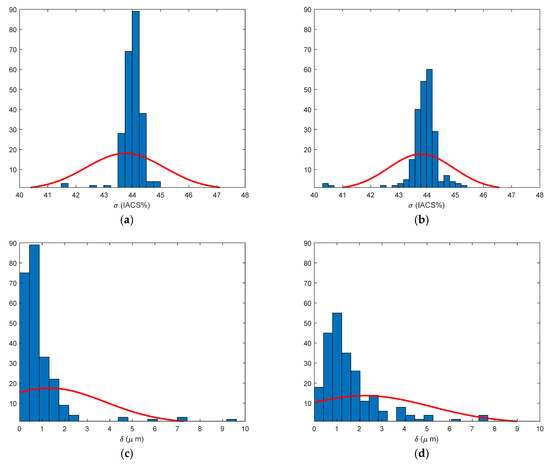
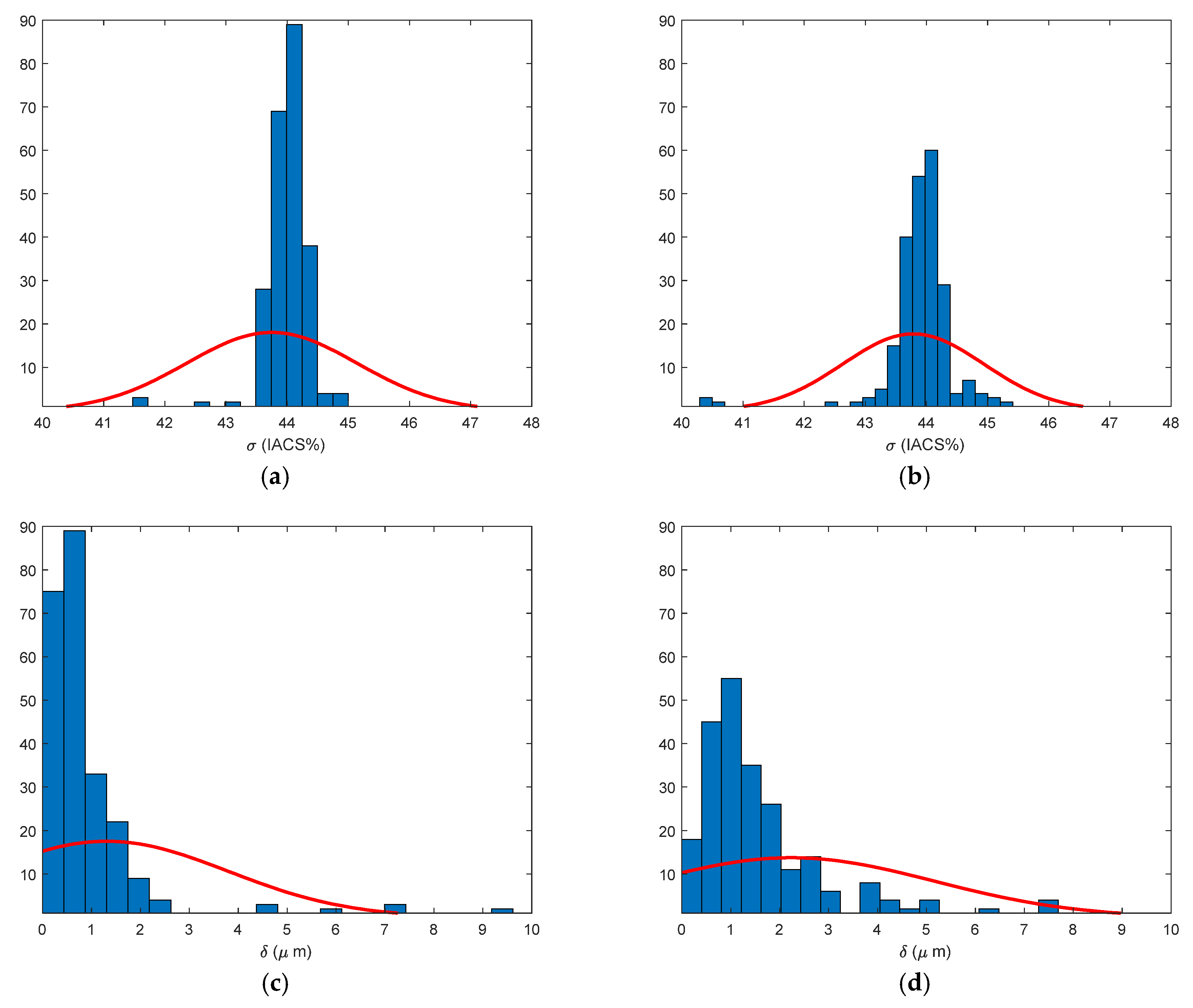
Results of the statistical processing of the datasets for the tested sample are presented in Figure 4. Electrical conductivity distribution of the sample at side A is presented in Figure 4a, electrical conductivity distribution of the sample at side B is presented in Figure 4b, lift-off gap distance of the sample at side A is presented in Figure 4c, and lift-off gap distance of the sample at side B is shown in Figure 4d. These results show excellent grouping around the mean and convex symmetrical distributions. Both sides have very similar mean values and standard distribution widths. Gaussian distribution curves and data histograms are visualized with different data bin groups that reflect differences in the amplitudes.
Figure 4.
Statistical processing of the results for the tested sample. Electric conductivity distribution of the sample at side A (a), electric conductivity distribution of the sample at side B (b), lift-off gap distance of the sample at side A (c), lift-off gap distance of the sample at side B (d).
MATLAB (R2022a) is used for statistical data processing and visualization of the results.
Table 1.
Statistical Results Summary.
Table 1 shows two groups of statistical results. The first group is the total for each sample—the mean μ and standard deviation St. The second group represents the directional means μ and standard deviations Stxx, Styy, and Stzz, according to Equation (4) and Equation (5). They are used for the composition of the 3D directional covariance matrix.
According to the directional results in Table 1, the largest variation is calculated in the z direction, which corresponds to the vertical printing direction, or the height of the sample during the WAAM welding process. This direction (z) shows the most significant inhomogeneity, nearly two to three times greater than that in the other directions (x, y). For the lift-off, which can be related to material density, the same inhomogeneity direction is clearly visible. The WAAM welding process exhibits greater property variation in the vertical-to-printing direction. It is significant compared to the other 3D printing directions, being two to three times greater, but it is small enough to represent a statistical variation of 43.75 ± 1.11, or a maximum variation of ±2.5% in the electrical properties during additive welding, which is an impressive result.
5. Conclusions
The WAAM 3D printing process for ER4043 aluminum alloy produces anisotropic material properties. Electrical conductivity distributions and surface lift-off have been measured during a surface mapping testing procedure. Measured datasets have been statistically estimated and compared. According to the directional results in Table 1, the largest variation is calculated in the z direction, which corresponds to the vertical printing direction or the height of the sample during the WAAM welding process. The WAAM welding process exhibits greater property variation in the vertical-to-printing direction (z). This variation is more significant compared to the other 3D printing directions, but it is small enough to represent a statistical variation in conductivity of less than 2.5%. It can be concluded that WAAM 3D printing produces stable electrical conductivity material properties, which are not fully isotropic but are acceptably close to actual isotropy. Electrical conductivity can be correlated with interlayer density and further with other known material properties such as mechanical strength and elasticity. These data can be used for improved additive manufacturing process control to enhance the electrical conductivity of aluminum WAAM samples. Correlation with surface or interlayer roughness is also of interest for future research work.
Author Contributions
Conceptualization, V.M., G.K., I.M., S.V., M.O. and D.S.; methodology, V.M., G.K., I.M., S.V., M.O. and D.S.; software, V.M., G.K., I.M., S.V., M.O. and D.S.; validation, V.M., G.K., I.M., S.V., M.O. and D.S.; formal analysis, V.M., G.K., I.M., S.V., M.O. and D.S.; investigation, V.M., G.K., I.M., S.V., M.O. and D.S.; Resources, V.M., G.K., I.M., S.V., M.O. and D.S.; data curation, V.M., G.K., I.M., S.V., M.O. and D.S.; writing—original draft, V.M., G.K., I.M., S.V., M.O. and D.S.; writing—review and& editing, V.M., G.K., I.M., S.V., M.O. and D.S.; Visualization, V.M., G.K., I.M., S.V., M.O. and D.S.; supervision, V.M. and I.M.; project administration, V.M. and S.V. All authors have read and agreed to the published version of the manuscript.
Funding
This research was funded by the National Science Fund of Bulgarian Ministry of Education and Science, Project #KP-06-N67/10 (2022).
Institutional Review Board Statement
Not applicable.
Informed Consent Statement
Not applicable.
Data Availability Statement
The results obtained in this study are included in the article. Further inquiries can be directed to the corresponding author.
Conflicts of Interest
The authors declare no conflicts of interest.
References
- Mateev, V.; Sinico, M.; Ghalamestani, S.G.; Van Hooreweder, B. Magnetic properties of as-built and heat treated M789 and M300 maraging steels produced via laser powder bed fusion. Next Mater. 2024, 6, 100287. [Google Scholar] [CrossRef] [Scilit]
- Ralchev, M.; Mateev, V.; Marinova, I. Magnetic Hysteresis Models for 3D Printed Composite Materials. In Proceedings of the IEEE International Magnetic Conference INTERMAG, Rio de Janeiro, Brazil, 5–10 May 2024; pp. 1–2. [Google Scholar]
- Kesarwani, S.; Yuvaraj, N.; Niranjan, M.S. Impact of depositional direction and current on microstructure and mechanical properties of the bimetallic wall of ER5356/ER4043 fabricated by cold metal transfer based wire arc additive manufacturing. CIRP J. Manuf. Sci. Technol. 2024, 53, 17–33. [Google Scholar] [CrossRef] [Scilit]
- Kotlarski, G.; Ormanova, M.; Valkov, S. Formation and Characterization of ER4043 Welding Wire Layers by CA-WAAM on Copper Substrates. Proc. Bulg. Acad. Sci. 2025, 78, 19–26. [Google Scholar] [CrossRef] [Scilit]
- Kazmi, K.H.; Das, A.K.; Sharma, S.K.; Mandal, A.; Shukla, A.K. Wire arc additive manufacturing of ER-4043 aluminum alloy: Evaluation of bead profile, microstructure, and wear behavior. Weld. World 2023, 67, 2187–2200. [Google Scholar] [CrossRef] [Scilit]
- Kazmi, K.H.; Sharma, S.K.; Das, A.K.; Mandal, A.; Kumar Shukla, A.; Mandal, R. Wire arc additive manufacturing of ER-4043 aluminum alloy: Effect of tool speed on microstructure, mechanical properties and parameter optimization. J. Mater. Eng. Perform. 2024, 33, 5120–5133. [Google Scholar] [CrossRef] [Scilit]
- Kesarwani, S.; Yuvaraj, N. Optimization of CMT-WAAM process parameters to minimize the porosity and surface roughness in bimetallic wall of aluminium alloys. Weld. World 2025, 69, 989–1002. [Google Scholar] [CrossRef] [Scilit]

Disclaimer/Publisher’s Note: The statements, opinions and data contained in all publications are solely those of the individual author(s) and contributor(s) and not of MDPI and/or the editor(s). MDPI and/or the editor(s) disclaim responsibility for any injury to people or property resulting from any ideas, methods, instructions or products referred to in the content. |
© 2026 by the authors. Licensee MDPI, Basel, Switzerland. This article is an open access article distributed under the terms and conditions of the Creative Commons Attribution (CC BY) license.