


Abstract
To effectively reduce the input current harmonics of the front-end rectifier for high-power electric vehicle chargers, this paper proposes a low-harmonic 36-pulse front-end rectifier equipped with a dual single-phase auxiliary rectifier pulse-tripling circuit (DSPAR-PTC). The proposed 36-pulse rectifier consists of a 12-pulse rectifier based on a medium-frequency power electronic transformer and the aforementioned DSPAR-PTC. According to the relationship between input and output voltages, the DSPAR-PTC operates in multiple conduction states to modulate and increase the number of output levels of the rectifier bridge. Based on the current characteristics of the AC and DC sides, the 12-pulse rectifier is upgraded to a 36-pulse topology. Thereby, the total harmonic distortion (THD) of the input current is reduced to one-third of the original value, and an approximately sinusoidal input current is achieved. The equivalent capacity of the DSPAR-PTC is only 3.7% of the rated output power, and no active power devices are required. It features a simple circuit structure, easy engineering implementation, and low cost. A 50 kW rectifier model is established on the Starsim HIL hardware-in-the-loop platform of Modeling Tech. The corresponding results verify the correctness of the theoretical analysis and demonstrate the harmonic suppression performance of the proposed topology.
1. Introduction
With the rapid development of the electric vehicle industry, the popularization of high-power charging piles has become a critical infrastructure to support industrial upgrading [1,2,3]. The performance of the rectifier, as its core component, directly determines the charging efficiency, power quality, and equipment miniaturization level [4,5]. In high-power application scenarios, the 12-pulse rectifier has become a preferred solution for the alternating current/direct current (AC/DC) conversion link of charging piles due to its advantages of reliable structure, low cost, and strong anti-interference capability [6,7]. Nevertheless, the conventional 12-pulse rectifier can theoretically cancel the fifth and seventh characteristic harmonics, while significant 11th and 13th harmonics still remain in the input current, resulting in a relatively high total harmonic distortion (THD) of the input current. Moreover, it relies on a low-frequency phase-shifting transformer, whose volume usually accounts for more than 70% of the total converter capacity, which severely restricts its application in charging pile fields sensitive to weight and volume [8,9].
To effectively reduce the volume and weight of phase-shifting transformers, researchers have proposed 12-pulse rectifier topologies adopting autotransformers. The application of autotransformers greatly reduces the volume and weight of the transformer. However, there is little difference between the input and output voltage levels of this scheme, and no electrical isolation exists between the input and output sides, which reduces the safety of the AC/DC converter [10,11]. To simultaneously satisfy the isolation function and volume reduction requirement of transformers, various power electronic transformers have been proposed successively [12,13]. Compared with conventional power electronic transformers, the power electronic phase-shifting transformer features a simpler circuit structure and control strategy owing to the unidirectional power flow [14,15]. Reference [16] proposes a medium-frequency 12-pulse rectifier based on a power electronic phase-shifting transformer, which remarkably reduces the volume and weight of the phase-shifting transformer. Nevertheless, the input line current THD of this scheme remains relatively high and often fails to meet industrial application requirements. Although further increasing the number of output voltage phases of the power electronic phase-shifting transformer can raise the pulse number of the AC/DC converter and reduce the input current THD, it will increase the design complexity of the transformer, make it difficult to guarantee winding symmetry, and lead to an exponential growth in the number of components. This further increases the system complexity, cost, and overall capacity burden [17].
References [18,19] introduce an auxiliary PWM rectifier into the secondary winding of the DC-side interphase reactor of a 12-pulse rectifier to indirectly modulate the output current of the rectifier bridge, thereby realizing harmonic suppression of the rectifier. This method can achieve satisfactory harmonic suppression performance, yet it suffers from relatively complex control of the auxiliary circuit and high cost.
To facilitate engineering implementation and improve system reliability, a 24-pulse rectifier with a double-tapped interphase reactor (DP-IPR) is proposed. By virtue of the alternate conduction of two diodes on the tap winding, additional operating modes are introduced, and the 12-pulse rectifier is extended to 24-pulse operation. This scheme features a simple circuit topology, high reliability, and easy implementation. However, the diodes on the tap are connected in series with the load path, resulting in considerable additional conduction loss. To reduce such additional conduction loss, a 24-pulse rectifier adopting a secondary-side rectification interphase reactor (SR-IPR) is proposed. Since the diodes in the SR-IPR are connected in parallel with the load, the additional conduction loss caused by series connection of diodes in the load path is eliminated, and the current stress of the auxiliary diodes is effectively reduced. Nevertheless, its harmonic suppression capability is limited and cannot meet the requirements of industrial applications.
Analysis of the 24-pulse rectifiers based on DP-IPR and SR-IPR indicates that although both topologies can multiply the pulse number of the rectifier, they differ in the modulation mechanism of rectifier bridge output current and the formation principle of DC-side circulating current. The DP-IPR scheme maintains the voltage characteristics of the interphase reactor unchanged, while the conduction mode of the SR-IPR scheme is solely determined by the relationship between the output voltage of the secondary winding and the load voltage. The operating ranges of the two schemes are both independent and overlapping, which makes the combined operation of DP-IPR and SR-IPR feasible.
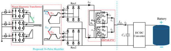
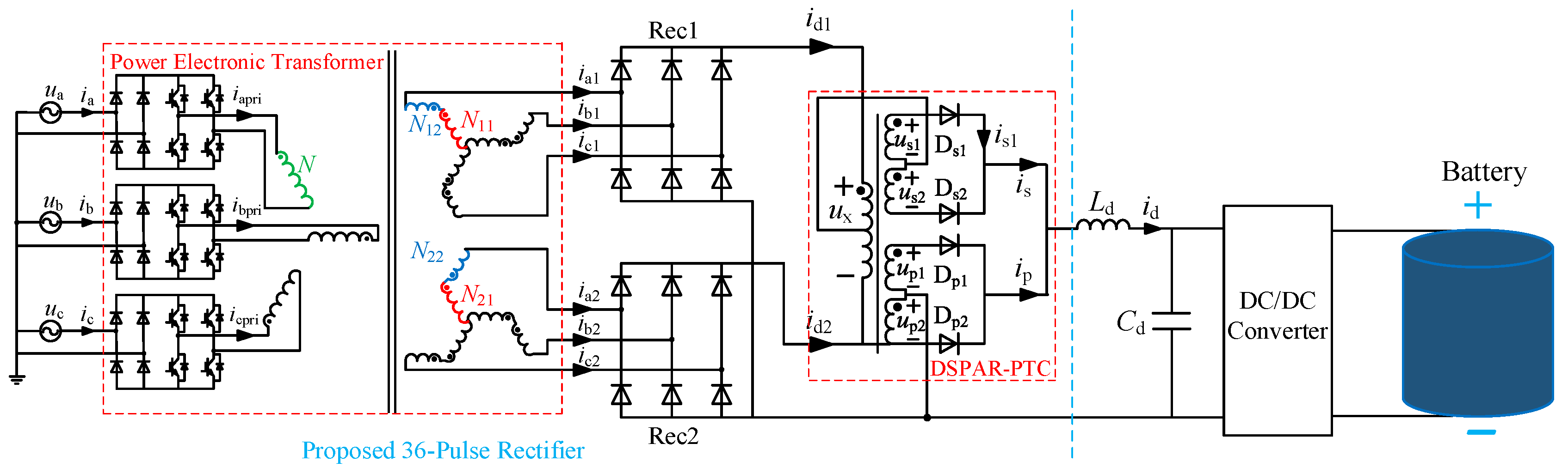
Therefore, to further improve the harmonic suppression capability of the front-end rectifier for high-power electric vehicle chargers, this paper proposes a low-THD 36-pulse front-end rectifier integrated with a dual single-phase auxiliary rectifier pulse-tripling circuit (DSPAR-PTC), as shown in Figure 1. Compared with the proposed 36-pulse rectifier topology, the DP-IPR and SR-IPR schemes feature lower equivalent capacity of the auxiliary circuit, which accounts for only 3.2% and 3.3% of the rated output power, respectively (3.7% for the proposed scheme). They also employ fewer devices with two fewer auxiliary diodes and thus have a slight advantage in hardware cost. Nevertheless, this cost advantage is achieved at the expense of harmonic suppression performance. The proposed DSPAR-PTC scheme can further reduce the total harmonic distortion (THD) of the input current by approximately one-third compared with the DP-IPR and SR-IPR schemes, achieving a remarkable improvement in harmonic suppression. Although the auxiliary circuit capacity increases slightly by 0.4–0.5% and two additional auxiliary diodes are adopted, leading to a limited increment in hardware cost, a substantial improvement in the power quality of the input current is obtained. The proposed DSPAR-PTC topology achieves a superior tradeoff between harmonic suppression performance and engineering implementation cost, exhibiting prominent application potential in high-power rectifier equipment.
Figure 1.
Schematic diagram of a high-power EV charger adopting the proposed 36-pulse rectifier.
2. Proposed Front-End Rectifier of EV Charger and Its Operating Modes
Figure 1 shows the schematic diagram of a high-power EV charger adopting the proposed 36-pulse rectifier, which consists of the proposed 36-pulse rectifier and the post-stage direct current/direct current (DC/DC) converter. The post-stage DC/DC converter is adopted to realize the control of the battery charging strategy, while the proposed 36-pulse rectifier acts as an interface circuit to obtain energy from the power grid. This paper mainly focuses on the research of the front-end 36-pulse rectifier, which is composed of a 12-pulse rectifier based on a medium-frequency power electronic transformer and the DSPAR-PTC.
2.1. Analysis of Working Principle of Medium-Frequency Power Electronic Transformer
Compared with the conventional 12-pulse rectifier adopting a power-frequency transformer, the medium-frequency power electronic transformer operates at a higher frequency. Consequently, the 12-pulse rectifier based on the medium-frequency power electronic transformer achieves a smaller volume. As indicated in reference [16], when the operating frequency of the transformer increases by approximately 10 times, its volume is reduced to about one-half of the original size. Therefore, a 12-pulse rectifier equipped with a medium-frequency power electronic transformer is adopted as the basic main circuit in this paper. To facilitate the subsequent analysis, the structure and basic operating principle of the phase-shift transformer in Figure 1 are introduced firstly.
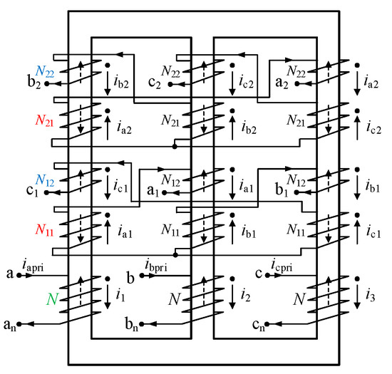
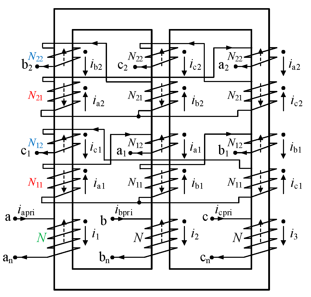
The winding structure of the medium-frequency phase-shift transformer is illustrated in Figure 2.
Figure 2.
Winding structure diagram of the medium-frequency phase-shifting transformer.
To achieve a phase difference of 30° between the two sets of output voltages of the transformer, the turns ratio of the primary and secondary windings of the phase-shifting transformer satisfies the following:
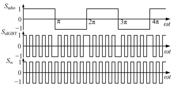
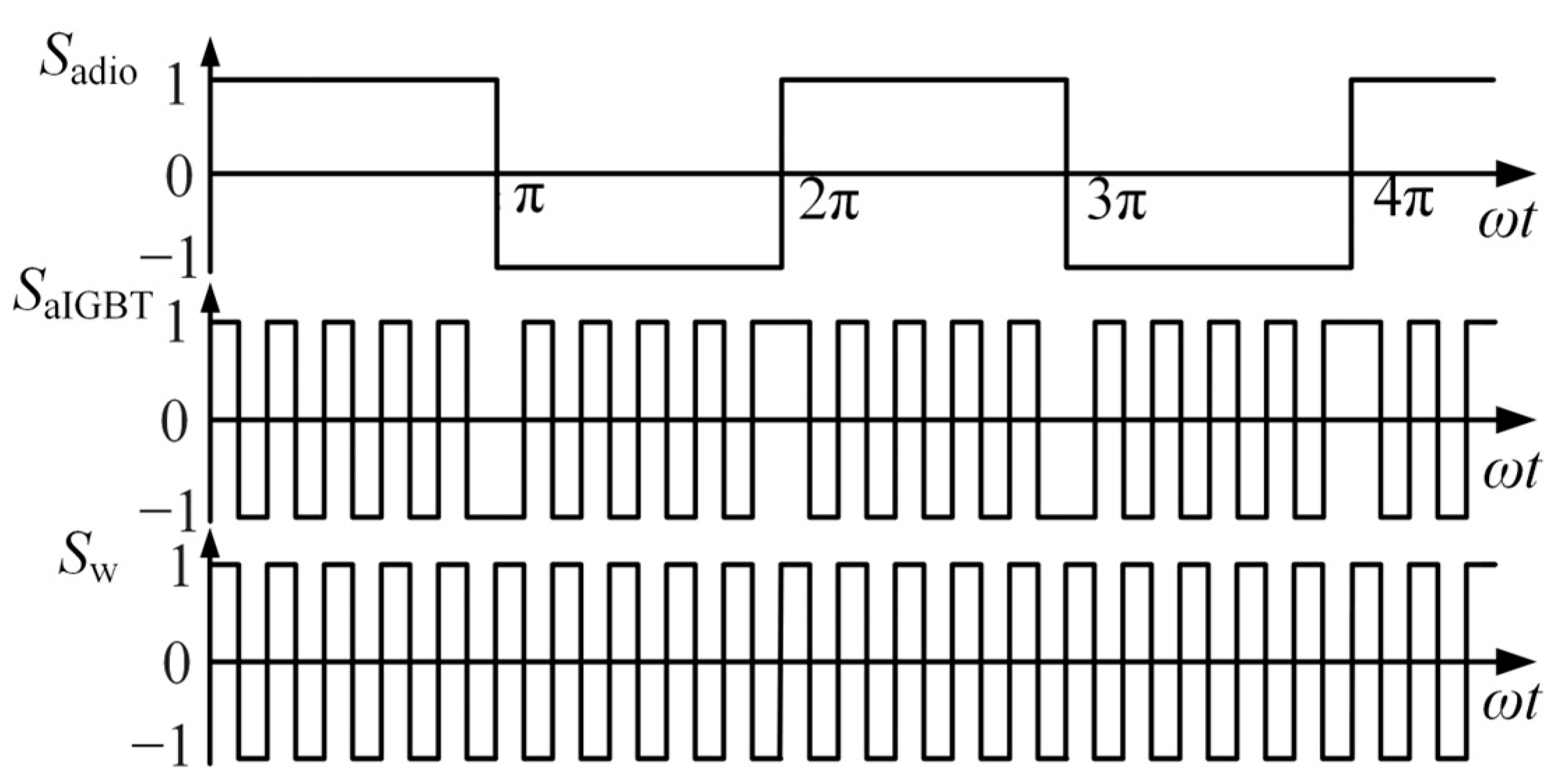
Figure 3 shows the switching function waveforms of the front-end alternating current/alternating current (AC/AC) converter of the medium-frequency power electronic transformer. Among them, Sadio is the switching function of the uncontrolled rectifier bridge in the phase-a bridge, SaIGBT denotes the switching function of the phase-a full-bridge inverter circuit, and Sw represents the overall switching function of the power electronic converter.
Figure 3.
Switching function waveforms of the power electronic converter.
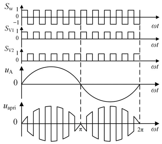
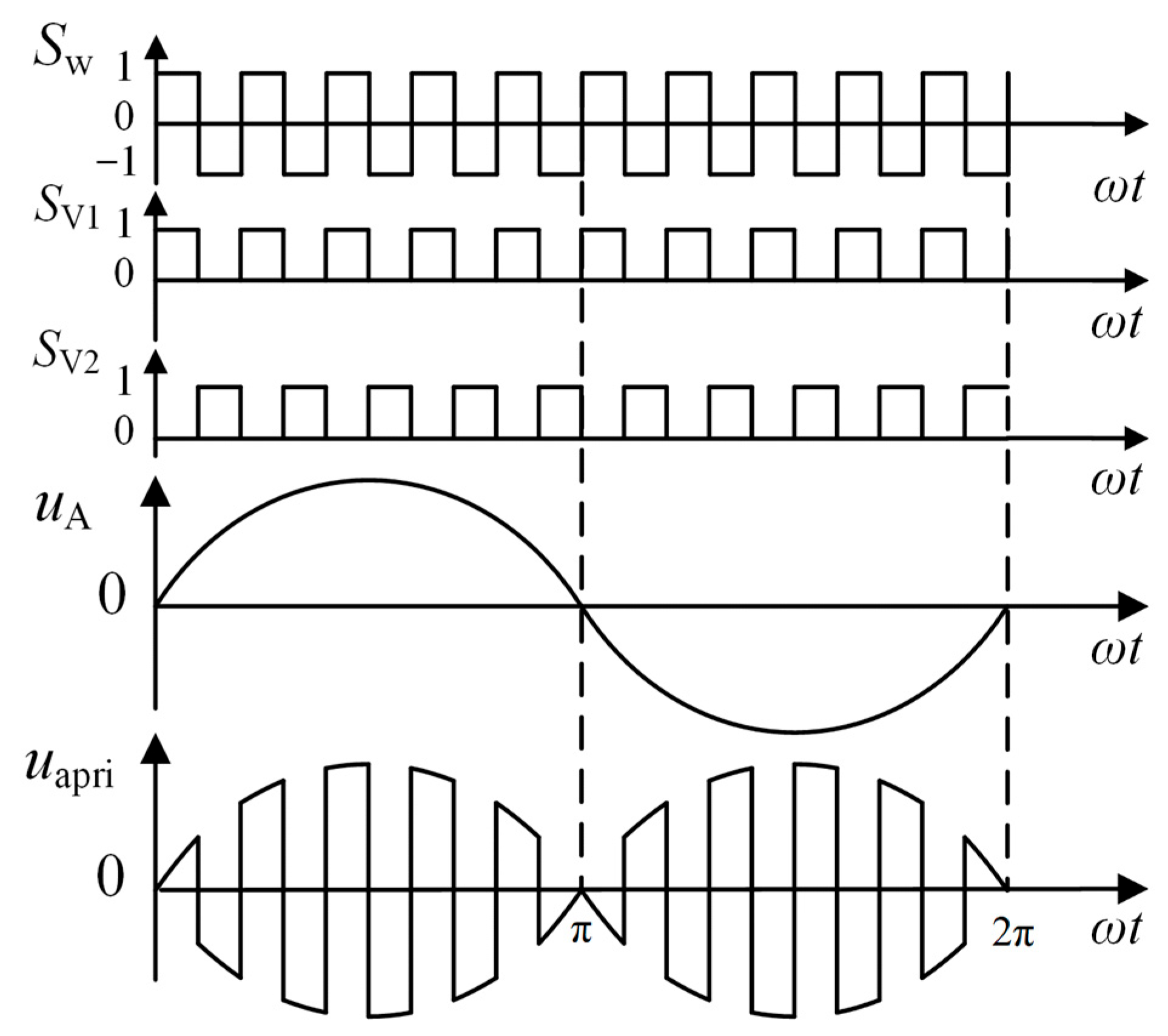
Figure 4 shows the main voltage waveforms of the power electronic converter. SV1 and SV2 are the control signals of the opposite switching devices in the full-bridge inverter circuit, uA is the waveform of the phase-A input voltage, and uapri represents the output voltage of the power electronic transformer.
Figure 4.
Voltage waveforms of the power electronic converter.
It can be seen from Figure 3 and Figure 4 that the power-frequency input voltage is modulated into a medium-frequency voltage with a sinusoidal envelope by the front-end AC/AC converter of the medium-frequency power electronic transformer. Consequently, the phase-shift transformer operates at medium frequency, which reduces the volume of the phase-shift transformer.
2.2. Analysis of Operating Modes of DSPAR-PTC
To facilitate the analysis of the operating modes of the DSPAR-PTC, the turns ratios p and m of the primary and secondary windings of the interphase reactor in the DSPAR-PTC are first defined according to Figure 1.
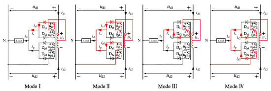
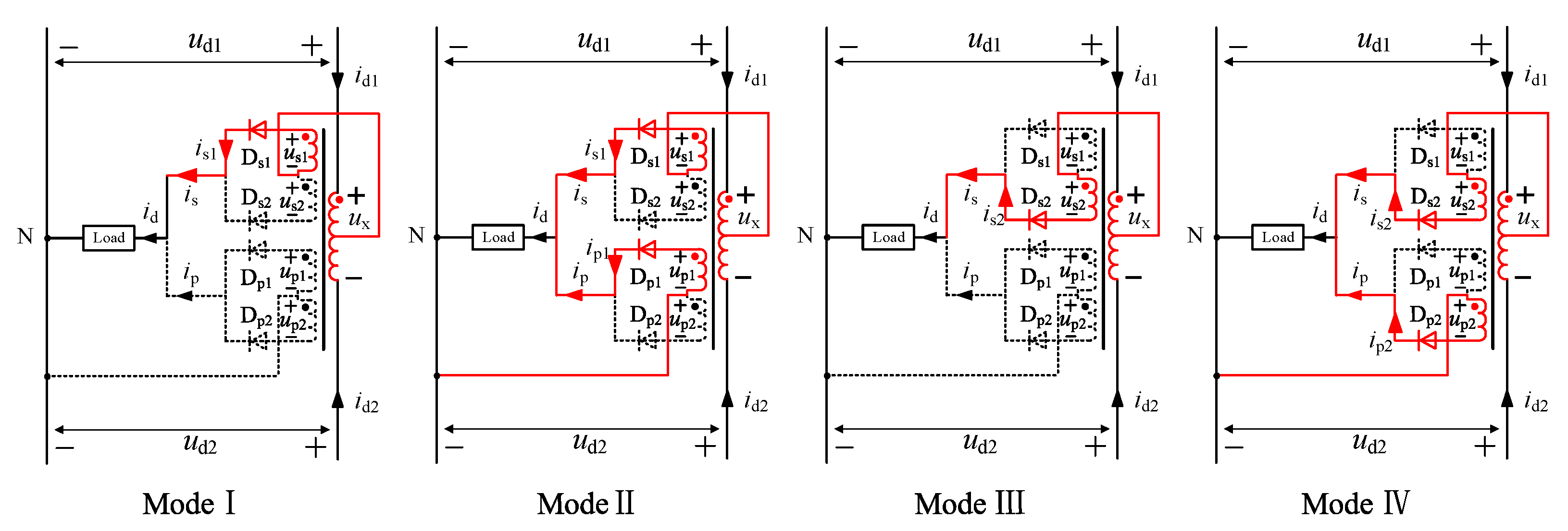
Based on the magnitude relationships among the voltages up1, up2 of the DSPAR-PTC and the output voltage ud of the rectification system, as well as the polarity of ux, the proposed rectifier has four operating modes as illustrated in Figure 5. Assuming that the load inductance in Figure 5 is sufficiently large, the load current id can be regarded as a constant value Id. The circuit operating state of each mode is analyzed, respectively, in the following.
Figure 5.
Operating modes of DSPAR-PTC.
Mode I: When up1 < ud, −up2 < ud, and ux > 0, the DSPAR-PTC operates in Mode I. Diodes Dp1 and Dp2 in the parallel branch are both reverse-biased, with the flowing currents ip1 and ip2 equal to zero, and the total output current ip is zero. Diode Ds1 conducts, carrying a current of is1, and the total output current of the series branch is is. The rectifier supplies power to the load through diode Ds1 connected in series with the load loop. The relationship between the output currents id1 and id2 of the three-phase rectifier bridges REC1 and REC2 and the load current Id are expressed as follows:
The relationships between the output voltages ud1, ud2 of REC1 and REC2 and the load voltage ud are as follows:
Mode II: When up1 > ud and ux > 0, the DSPAR-PTC enters Mode II. The diode Dp1 conducts with a flowing current of ip1, and the total output current is ip. The diode Ds1 conducts with a current of is1, and the total output current is is. The rectifier supplies power to the load jointly through Dp1 in parallel with the load and Ds1 connected in series with the load loop. The output currents the output currents id1, id2 of REC1 and REC2 can be expressed in terms of the load current Id as follows:
The load voltage ud can be represented by the output voltages ud1, ud2 of of REC1 and REC2 as follows:
Mode III: When up1 < ud, −up2 < ud, and ux <0, the DSPAR-PTC works in Mode III. Diodes Dp1 and Dp2 are both reverse-biased, the currents ip1 and ip2 flowing through them are zero, and the total output current ip is zero. Diode Ds2 conducts with a current of is2, and the total output current is is. The rectifier supplies power to the load through diode Ds2 connected in series with the load loop. Applying Kirchhoff’s current law (KCL), the output currents id1, id2 of REC1 and REC2 are related to the load current Id as follows:
Based on Kirchhoff’s voltage law (KVL), the load voltage ud is derived as follows:
Mode IV: When −up2 > ud and ux < 0, the DSPAR-PTC runs in Mode IV. The diode Dp2 conducts with a current of ip2, and the total output current is ip. The diode Ds2 conducts with a current of is2, and the total output current is is. The rectifier supplies power to the load jointly through diode Dp2 in parallel with the load and diode Ds2 connected in series with the load loop. From Kirchhoff’s current law (KCL), the output currents id1, id2 of REC1 and REC2 can be derived in terms of the load current Id as follows:
Based on Kirchhoff’s voltage law (KVL), the relationships between the output voltages ud1, ud2 of REC1 and REC2 and the load voltage ud can be expressed as follows:
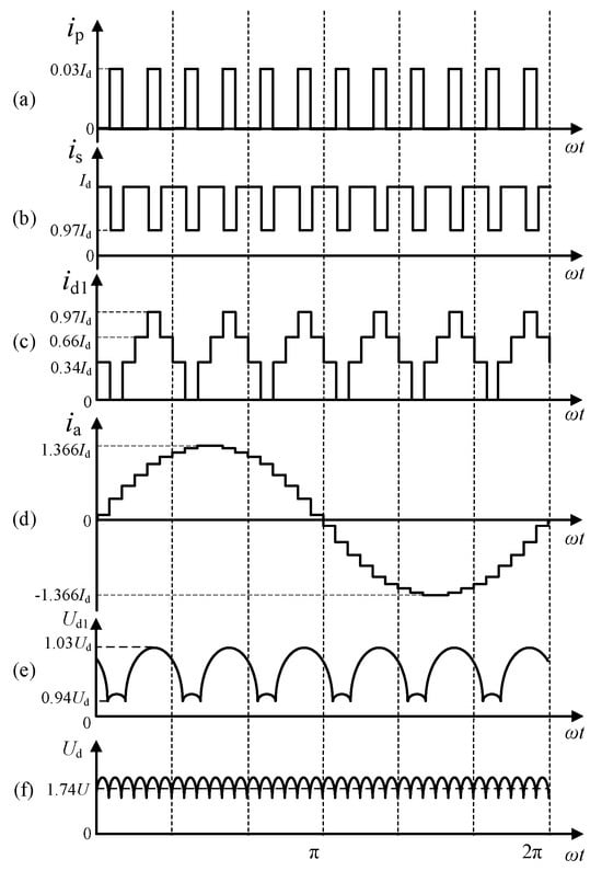
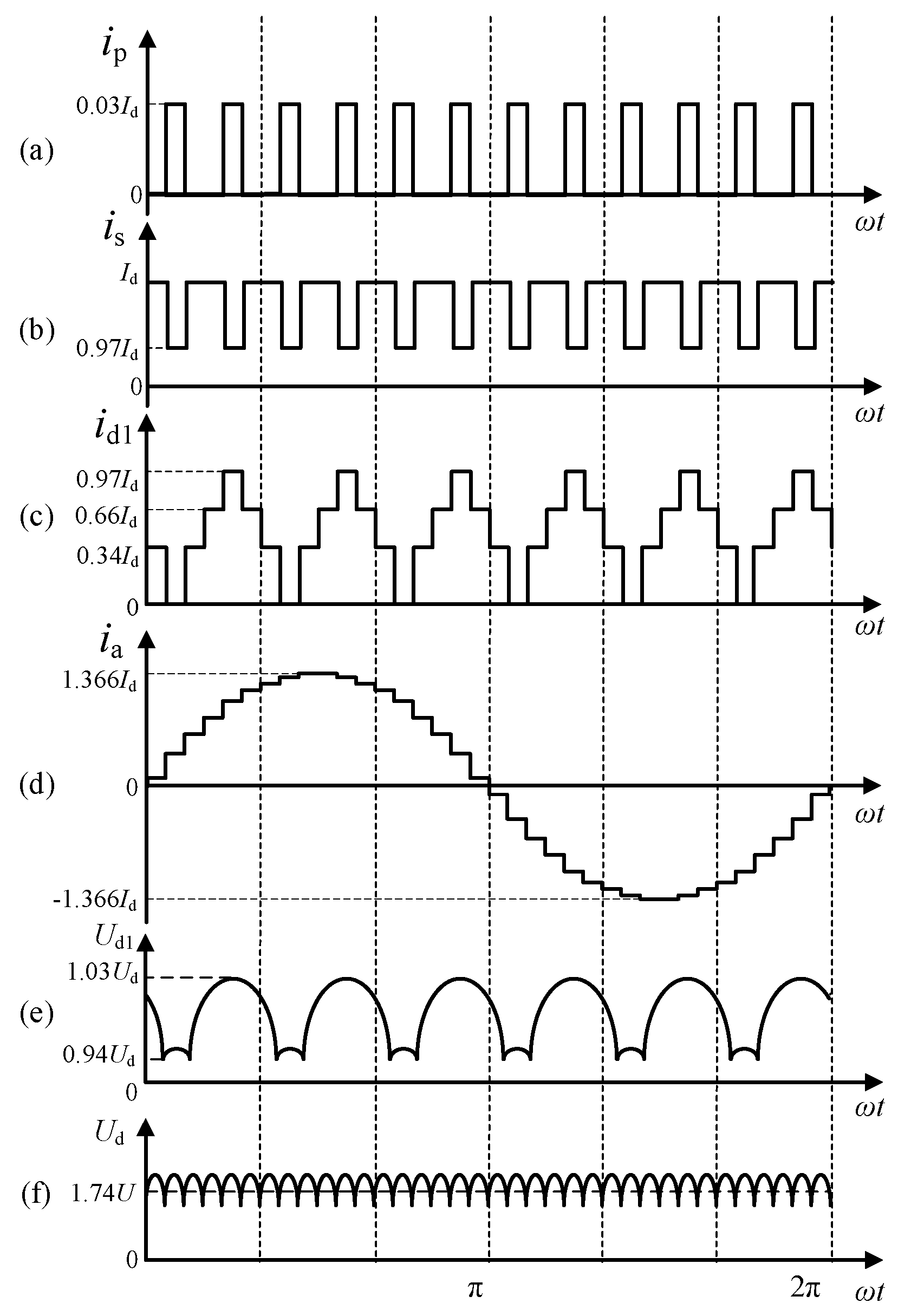
when the DSPAR-PTC operates under the optimal turns ratio condition, the main current and voltage waveforms of the rectifier circuit are shown in Figure 6.
Figure 6.
Main current and voltage waveforms of the rectifier. (a) Output current ip of the auxiliary rectifier connected in series with the load. (b) Output current is of the auxiliary rectifier connected in parallel with the load. (c) Output current id1 of REC1. (d) Input current ia of the proposed rectifier. (e) Output voltage ud1 of REC1 (f) Output voltage ud of the proposed rectifier.
3. Optimal Turns Ratio of DSPAR-PTC
From the analysis of the operating modes of the DSPAR-PTC, it can be seen that the turns ratios p and m determine the output current and voltage of the rectifier bridge. To obtain the optimal turns ratio that minimizes the THD of the rectifier input current and the output voltage ripple, it is necessary to optimize the turns ratios of the DSPAR-PTC.
3.1. Turns Ratio of DSPAR-PTC at Minimum Input Current THD
Based on the winding connection structure of the phase-shifting transformer shown in Figure 2 and the ampere-turn balance principle, the relationship between the primary current of the medium-frequency phase-shifting transformer and the input current of the three-phase rectifier bridge satisfies the following:
The relationships between the input currents of REC1 and REC2 and their output currents id1, id2 are as follows:
where Sw is the switching function of the power electronic converter, and Sa1 is the switching function corresponding to the input current ia1 and output current id1 of REC1.
Sa1 can be expressed as follows [16]:
According to the phase relationship between the input voltages of REC1 and REC2, the switching functions satisfy the following relation [16]:
Combined with the rectifier topology in Figure 1, the corresponding relationship between the grid-side input current and the primary current of the medium-frequency phase-shifting transformer is as follows [16]:
Since the three-phase input current waveforms of the rectifier are phase-shifted by 120° from each other, only the phase-A input current is discussed. Substituting Equations (11) and (12) into Equation (15) yields the following:
The switching function of the power electronic converter is a square wave with a frequency of 500 Hz and an amplitude of 1, and SW2 is constantly equal to 1. The 500 Hz operating frequency is selected for the AC/AC converter by considering the tradeoff between transformer size, power losses, thermal performance, and engineering feasibility. Increasing the operating frequency can reduce transformer size; however, it also increases core and AC copper losses, semiconductor switching losses, EMI, and thermal-management requirements, while imposing more stringent requirements on magnetic materials and manufacturing processes. In contrast, 500 Hz allows the use of mature thin-gauge silicon steel sheets while providing a substantial reduction in transformer volume and weight compared with the conventional 50 Hz operation. Therefore, 500 Hz offers a favorable balance among transformer size, efficiency, material cost, manufacturing complexity, and system reliability, and is selected as the operating frequency of the transformer in this study.
According to the operating modes of the rectifier, the output currents id1 and id2 of REC1 and REC2 can be expressed within one cycle as follows:
where θ denotes the electrical angle at which the operating mode transition of the DSPAR-PTC is first realized within the range [0, π/12], and it satisfies the following:
where the electrical angle θ is related to the turns ratios m and p by the following:
ud(θ) = m|up1(θ)|
Substituting Equations (13), (14), (17), and (18) into Equation (16), the expression of ia over a quarter cycle can be derived as follows:
It can be seen from Equation (21) that the THD of the input current ia is determined by the turns ratios p and m of the DSPAR-PTC.
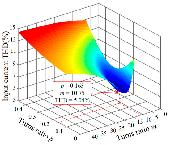
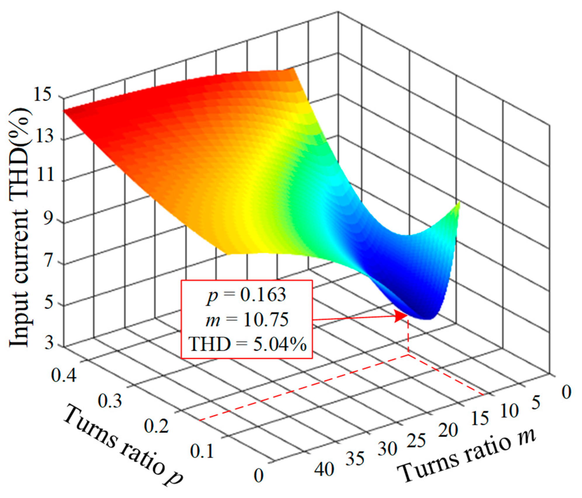
Figure 7 illustrates the relationship between the THD of the input current and the turns ratios p and m of the DSPAR-PTC.
Figure 7.
Relationship between input current THD and turns ratios p and m.
It can be observed from Figure 7 that when the turns ratios of DSPAR-PTC are p = 0.163 and m = 10.75, the THD of the input current ia reaches a minimum value of 5.04%, which agrees well with the theoretical value for a conventional 36-pulse rectifier. At this point, the harmonics of the grid-side current are suppressed to the maximum extent.
3.2. Turns Ratio of DSPAR-PTC at Minimum Output Voltage Ripple
Let the grid-side supply voltage of the rectifier circuit be as follows:
where Um is the amplitude of the input phase voltage.
According to the winding connection structure of the phase-shifting transformer shown in Figure 2, the output voltage of the secondary windings of the phase-shifting transformer satisfies the following:
Based on the above analysis of the operating modes of the DSPAR-PTC, the output voltages of REC1 and REC2 satisfy the following relations in the interval [0, π/3], respectively:
The load voltage ud satisfies the following relation over the interval [0, π/12]:
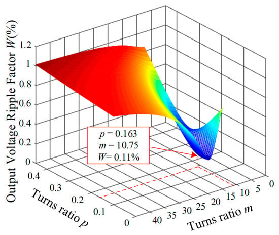
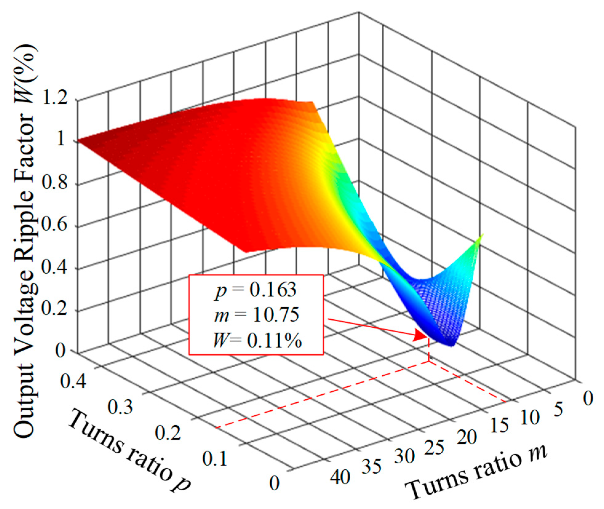
It can be seen from Equation (27) that the ripple factor W of the load-side output voltage is also determined by the turns ratios p and m of the DSPAR-PTC. Figure 8 presents the relationship between the output voltage ripple factor W and the turns ratios p and m of the DSPAR-PTC.
Figure 8.
Relationship between output voltage ripple factor W and turns ratios p and m.
It can be seen from Figure 8 that when the turns ratios of the DSPAR-PTC are p = 0.163 and m = 10.75, the output voltage ripple factor W also reaches its minimum value of 0.11%.
Combining the input current THD and the output voltage ripple, it can be concluded that the rectifier circuit achieves the optimal harmonic suppression performance at p = 0.163 and m = 10.75, and the proposed circuit operates as a standard 36-pulse rectifier circuit.
4. Capacity Analysis of DSPAR-PTC
To clarify the influence of the proposed method on system capacity and provide a reference for the design of DSPAR-PTC, the capacity of DSPAR-PTC is analyzed under the optimal turns ratio condition.
The corresponding value of θ under the optimal turns ratio condition is as follows:
The expression for the primary-side voltage Ux of the DSPAR-PTC within one operating period [0, π/3] is as follows:
According to Equation (29), the effective value of the primary winding voltage Ux of the DSPAR-PTC satisfies the following:
According to the relationship between the primary and secondary windings of the DSPAR-PTC, combined with Equations (2) and (30), the effective values of voltages Us1, Us2, Up1, and Up2 can be derived to satisfy, respectively, the following:
Us1_rms = Us2_rms = pUx_rms = 0.011Ud
Up1_rms = Up2_rms = mUx_rms = 0.742Ud
The currents is1 and is2 satisfy the following:
The parallel branch currents ip1 and ip2 satisfy the following:
Based on Equations (17), (18) and (33)–(36), and the definition of effective value, the effective values of id1, id2, is1, is2, ip1, and ip2 satisfy the following:
Therefore, the capacity of the DSPAR-PTC satisfies the following:
It can be concluded from the above analysis that the capacity of the DSPAR-PTC is quite small, accounting for only 3.7% of the rated power. Therefore, the scheme proposed in this paper is suitable for high-power applications.
5. Loss Analysis
Taking the 50 kW output power considered in the manuscript as an example, and based on [20] and the parameters listed in Table 1, the transformer losses are evaluated as follows.
Table 1.
Parameters for calculating transformer losses.
The core loss and copper loss of the transformers can be expressed as follows:
where mc, kc, Bm, α, fT, and β denote the transformer core mass, material coefficient, maximum flux density, flux-density exponent, operating frequency, and frequency exponent, respectively. In addition, J, ρCu, Lmlti, Ki, Ni, and Ii represent the current density, copper resistivity, mean turn length of the ith winding, AC/DC resistance coefficient, number of turns of the ith winding, and RMS current of the ith winding, respectively.
According to (41) and (42), using the parameters listed in Table 1, the total loss of the 50 kW power electronic transformer, with a maximum flux density of 1.25 T and an operating frequency of 500 Hz, is approximately 611 W. In comparison, the power-frequency isolated phase-shifting transformer used in the conventional 36-pulse rectifier, with a maximum flux density of 1.4 T and an operating frequency of 50 Hz, has a total loss of approximately 700 W. The loss of the DSPAR-PTC is approximately 386 W, while the loss of the 36-pulse rectifier IPR is approximately 477 W.
According to [20], the diode loss can be expressed as follows:
where Vf denotes the forward voltage drop of the diode and represents its equivalent on-state resistance. Based on the parameters of the experimental prototype and (43), the diode loss of the proposed 36-pulse rectifier based on the power electronic transformer is calculated to be approximately 623 W, whereas that of the conventional 36-pulse rectifier is approximately 550 W.
Using the same device-loss calculation method, the IGBT losses can also be evaluated. The total IGBT loss mainly consists of conduction loss and switching loss, which can be expressed as follows:
The calculated total IGBT loss is approximately 703 W. Based on the above analysis, under the operating conditions of the experimental prototype, the total loss of the proposed 36-pulse rectifier based on the power electronic transformer is approximately 2.32 kW, whereas that of the conventional 36-pulse rectifier is approximately 1.73 kW. The increase in total loss is mainly attributed to the additional IGBT losses introduced by the DSPAR-PTC. Although the proposed rectifier incurs a certain increase in power loss, the modulation capability of the IGBTs effectively reduces the size and weight of the phase-shifting transformer, thereby providing a favorable tradeoff between power loss and transformer volume and weight.
6. Hardware-in-the-Loop Platform Verification
To verify the correctness of the above theoretical analysis and the pulse-multiplication effect of the DSPAR-PTC, real-time hardware-in-the-loop (HIL) tests are conducted using the StarSim HIL platform developed by Modeling Tech. The topology adopted for the HIL test is shown in Figure 1, where the proposed 36-pulse rectifier is employed as the front-end stage and an LLC DC/DC converter is used as the downstream stage. The main parameters of the HIL simulation model are listed in Table 2.
Table 2.
Main parameters of the simulation model.
In the HIL test system, the DSP controller is implemented using a TMS320F28335, while the power-stage model, including the input- and output-side electrical characteristics, is executed in real time on the MT6020 platform using StarSim HIL. The DSP controller and the MT6020 exchange control and feedback signals in real time, thereby forming a closed-loop HIL test system.
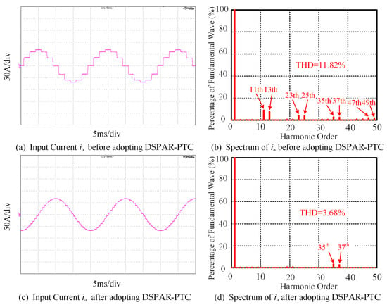
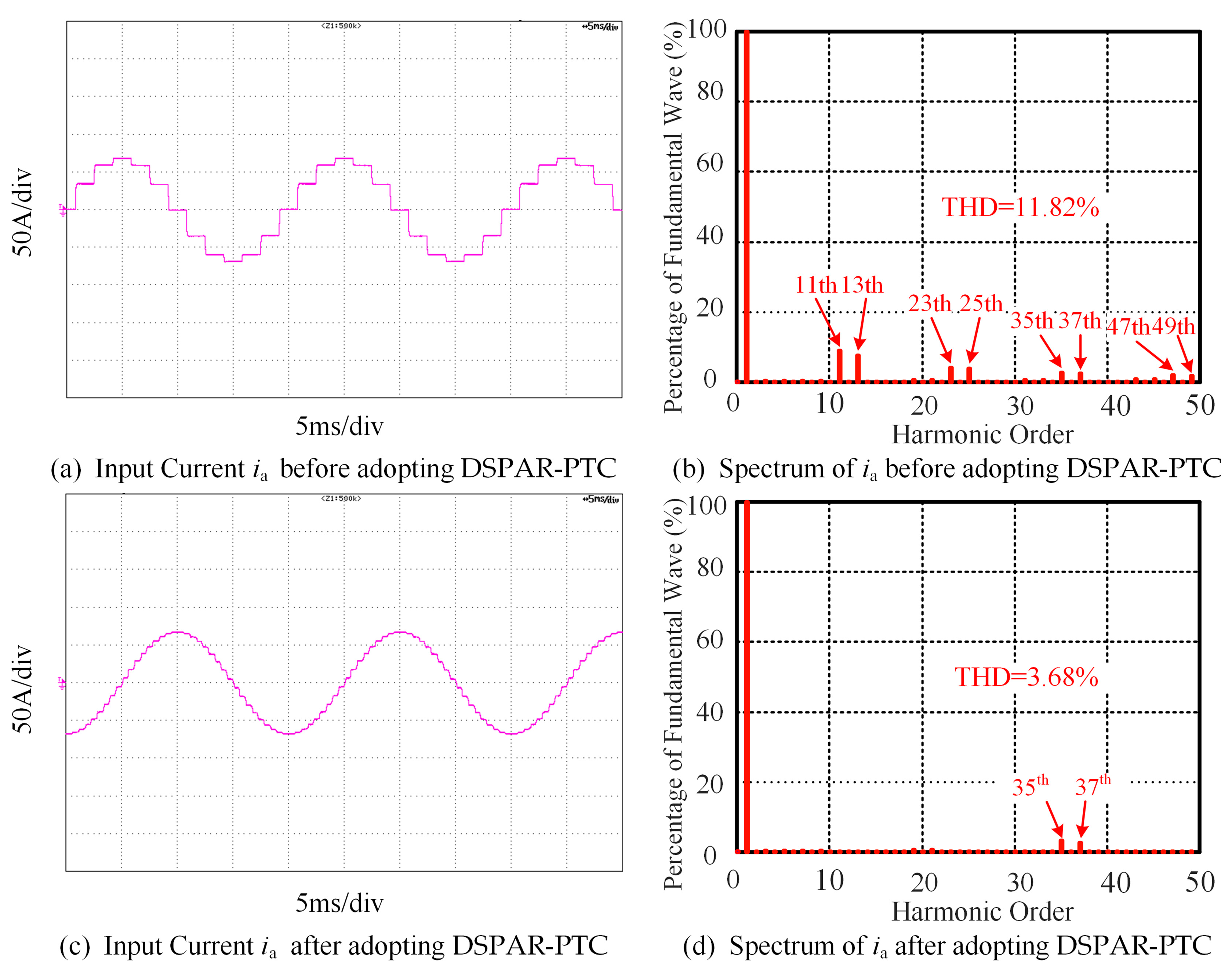
To verify the pulse multiplication effect of the DSPAR-PTC, Figure 9 illustrates the input current and its spectrum of the rectifier before and after the DSPAR-PTC is connected to the DC side.
Figure 9.
Input current and its spectrum of the rectifier.
As shown in Figure 9a, before the adoption of the DSPAR-PTC, the rectifier operates as a conventional 12-pulse rectifier, where the input current is a 12-step waveform and the THD of the input current is 11.82%. As shown in Figure 9b, after adopting the DSPAR-PTC, the number of steps of the rectifier input current increases from 12 to 36, and the THD of the input current is reduced from 11.82% to 3.68%. Due to the filtering effect of the transformer leakage inductance, the THD of the input current (3.68%) is slightly lower than the theoretical value (5.04%).
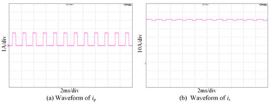
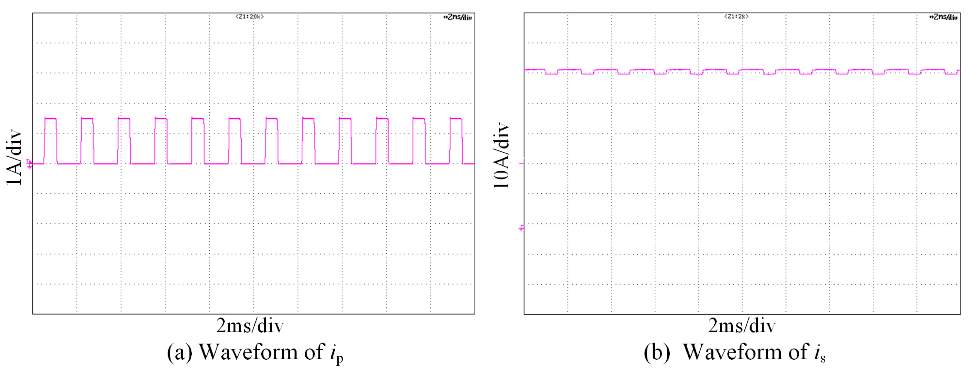
The main current waveforms of the DSPAR-PTC are shown in Figure 10.
Figure 10.
Main current waveforms of DSPAR-PTC.
As illustrated in Figure 10a, the total output current ip of the parallel unit is a square-wave current with a frequency of 600 Hz and an amplitude of 1.5 A, which accounts for only 3% of the load current. This result is consistent with the theoretical analysis in Figure 6a. Figure 10b shows the total output current is. Since the sum of is and ip equals the load current, the ripple amplitude of is is relatively small, which is in good agreement with the theoretical analysis presented in Figure 6b.
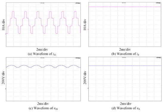
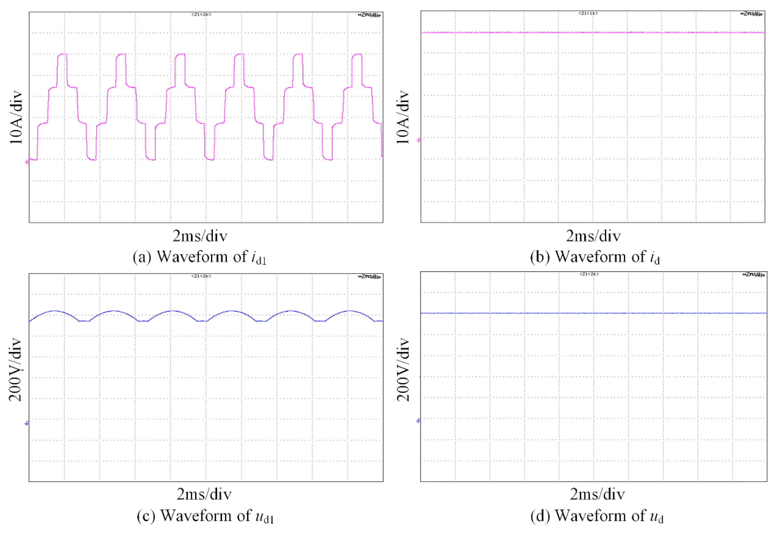
Figure 11 shows the main current and voltage waveforms of the rectifier.
Figure 11.
Main current and voltage waveforms of the rectifier.
Figure 11a presents the output current id1 of rectifier bridge REC1, which is modulated into a four-level DC current with a frequency of 300 Hz, consistent with the theoretical analysis in Figure 6c. Figure 11c illustrates the output voltage ud1 of rectifier bridge REC1, which is modulated into a four-level DC voltage at 300 Hz, and agrees well with the theoretical analysis in Figure 6e. It can be observed from Figure 11b,d that the ripples of the rectifier output current id and output voltage ud are small, and the power quality is greatly improved.
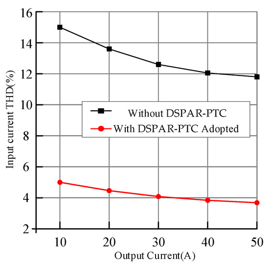
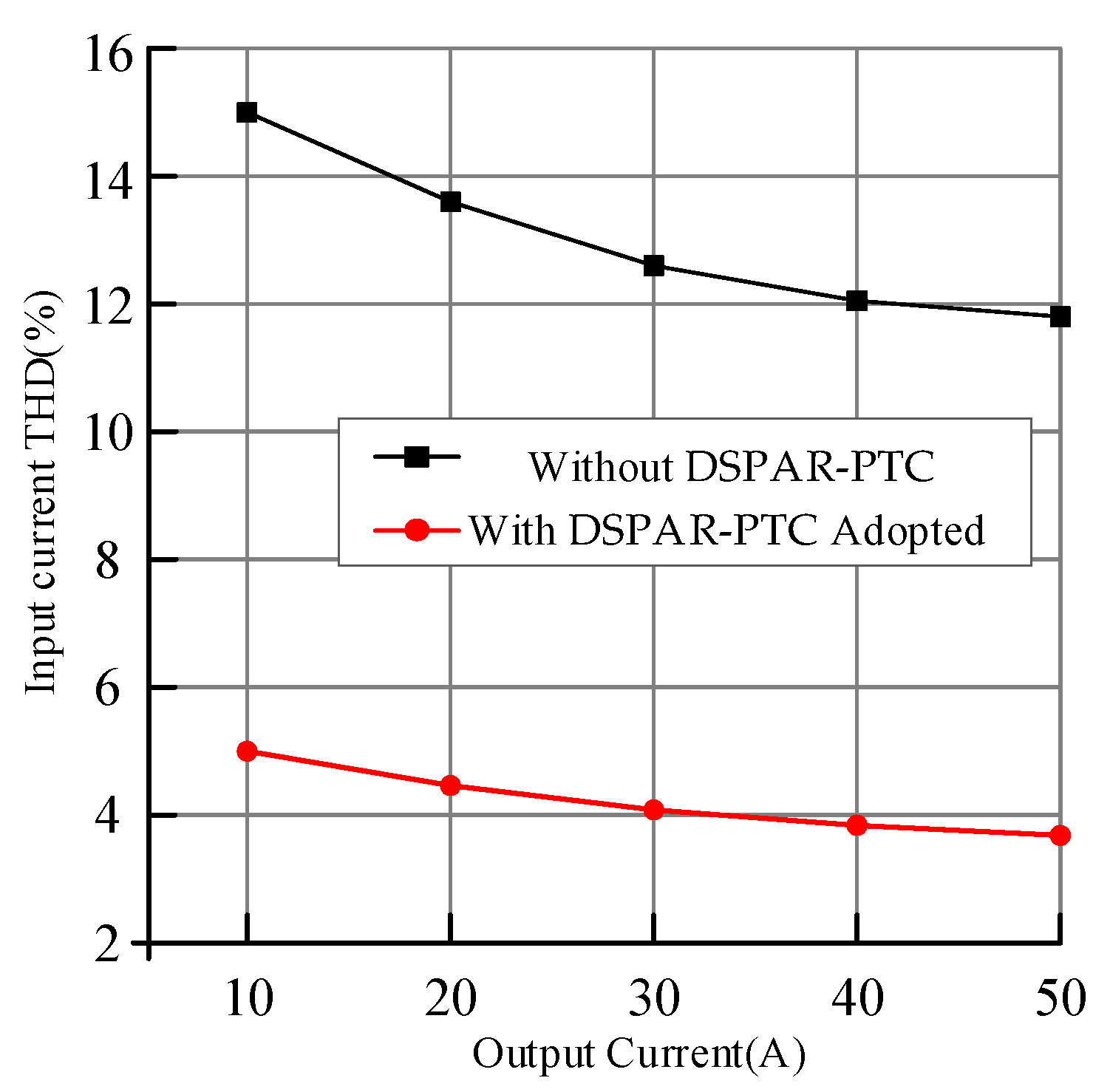
To clarify the harmonic suppression performance of the proposed rectifier under different load conditions, the input current THD is tested at load currents of 10 A, 20 A, 30 A, 40 A, and 50 A, respectively. The curve of the input current THD of the proposed rectifier varying with the load is shown in Figure 12.
Figure 12.
Curve of input current THD versus load.
As shown in Figure 12, the input current THD of the proposed rectifier remains below 5.04% over a wide load variation range, indicating that the rectifier maintains excellent harmonic suppression performance within a broad variation range of load current.
7. Conclusions
To reduce the volume, weight, and input current harmonics of the front-end rectifier for high-power electric vehicle chargers, this paper proposes a novel 36-pulse rectifier integrating a medium-frequency power electronic transformer and a DSPAR-PTC. The operating modes of the proposed DSPAR-PTC and the working principle of the medium-frequency power electronic transformer are analyzed. The optimal turns ratio of the DSPAR-PTC is derived under the minimum THD of the input current and minimum output voltage ripple. The analysis results show that when the optimal turns ratio is adopted for the DSPAR-PTC, the input current THD is reduced to one-third of its original value, decreasing from 11.82% to 3.68%. The input current harmonics can be effectively suppressed, and the equivalent capacity of the DSPAR-PTC is only 3.7% of the output power. The proposed DSPAR-PTC scheme features simple circuit structure, low cost, easy implementation, and high reliability, and possesses a good engineering application prospect.
Author Contributions
Conceptualization, Y.H., J.Y. and S.L.; methodology, J.Y. and S.L.; analysis, H.Z., L.J., Z.Z. and J.Y.; validation, H.Z., L.J. and Z.Z.; data curation, H.Z., L.J., Z.Z. and J.Y.; writing, Y.H., J.Y., S.L., H.Z. and L.J. All authors have read and agreed to the published version of the manuscript.
Funding
This research was funded by the Science and Technology Project of State Grid Shandong Electric Vehicle Service Co., Ltd., grant number V6000001107F.
Data Availability Statement
The data presented in this study are available on request from the corresponding authors due to privacy and commercial confidentiality restrictions.
Conflicts of Interest
Authors Yan Han, Hui Zhou, Liyang Jiang, Zhi Zhu and Sihua Liu were employed by the company STATE GRID SHANDONG ELECTRIC VEHICLE SERVICE Co., Ltd. Author Jiahao Yin was employed by the company Xj Power Co., Ltd. All authors declare that the research was conducted in the absence of any commercial or financial relationships that could be construed as a potential conflict of interest.
Nomenclature
| Symbol | Units | Definition |
| N | turns | Primary winding turns of the phase-shifting transformer |
| Ni | turns | Secondary winding turns of the phase-shifting transformer |
| Sadio | Switching function of the uncontrolled rectifier bridge | |
| SaIGBT | Switching function of the full-bridge inverter circuit | |
| Sw | Overall switching function of the power electronic converter | |
| SVi | Control signals of the opposite switching devices in the full-bridge inverter circuit | |
| Sai, Sbi, Sci | Switching function of the three-phase rectifier bridge | |
| uA | V | Phase-A input voltage |
| uapri | V | Output voltage of the power electronic transformer |
| p, m | turns | Turns ratio of the interphase reactor |
| Usi, Upi, Ux | V | Winding voltage of the interphase reactor |
| isi, ipi, ix | A | Current flowing through the winding of the interphase reactor |
| iai, ibi, ici | A | Input currents of the three-phase rectifier bridges |
| id1, id2 | A | Output current of the three-phase rectifier bridge |
| ud1, ud2 | V | Output voltage of the three-phase rectifier bridge |
| id | A | Output current of the rectifier |
| ud | V | Output voltage of the rectifier |
| ia | A | Input current of the rectifier |
References
- Umesh, B.S.; Khadkikar, V.; Zeineldin, H.; Singh, S.; Otrok, H.; Mizouni, R.; Rathore, A. A combinatory AC and DC charging approach for electric vehicles. IEEE Trans. Intell. Transp. Syst. 2024, 25, 15467–15476. [Google Scholar] [CrossRef] [Scilit]
- Acharige, S.S.G.; Haque, E.; Arif, M.T.; Hosseinzadeh, N.; Hasan, K.N.; Oo, A.M.T. Review of electric vehicle charging technologies, standards, architectures, and converter configurations. IEEE Access 2023, 11, 41218–41255. [Google Scholar] [CrossRef] [Scilit]
- Khan, M.S.U.; Thurlbeck, A.; Watt, E.; Kisacikoglu, M.J.; Ucer, E.; Meintz, A.; Mahmud, R. Development and experimental validation of a high-power DC distribution testbed for advanced charging infrastructure and energy management. IEEE Trans. Ind. Appl. 2025, 61, 7646–7655. [Google Scholar] [CrossRef] [Scilit]
- Singh, B.; Gairola, S.; Singh, B.N.; Chandra, A.; Al-Haddad, K. Multipulse AC-DC converters for improving power quality: A review. IEEE Trans. Power Electron. 2008, 23, 260–281. [Google Scholar] [CrossRef] [Scilit]
- Safayatullah, M.; Elrais, M.T.; Ghosh, S.; Rezaii, R.; Batarseh, I. A comprehensive review of power converter topologies and control methods for electric vehicle fast charging applications. IEEE Access 2022, 10, 40753–40793. [Google Scholar] [CrossRef] [Scilit]
- Bai, S.; Lukic, S.M. Unified active filter and energy storage system for an MW electric vehicle charging station. IEEE Trans. Power Electron. 2013, 28, 5793–5803. [Google Scholar] [CrossRef] [Scilit]
- Suraj, G.O.; Reddy, M.R.; Reddy, B.D. A novel topology and design methodology for improved power quality of high-power charger. IEEE Trans. Ind. Electron. 2025, 72, 80–88. [Google Scholar] [CrossRef] [Scilit]
- Chen, J.; Shen, J.; Chen, J.; Shen, P.; Song, Q.; Gong, C. Investigation on the selection and design of step-up/down 18-pulse ATRUs for more electric aircraft. IEEE Trans. Transp. Electrif. 2019, 5, 795–811. [Google Scholar] [CrossRef] [Scilit]
- Tsai, M.-T.; Chu, C.-L.; Chen, Y.-J.; Chen, B.-X. Design a high-frequency isolated AC-DC converter for high current applications. In Proceedings of the 2015 IEEE International Telecommunications Energy Conference (INTELEC), Osaka, Japan, 18–22 October 2015; pp. 1–6. [Google Scholar]
- Singh, B.; Bhuvaneswari, G.; Garg, V. An improved power-quality 30-pulse AC-DC for varying loads. IEEE Trans. Power Deliv. 2007, 22, 1179–1187. [Google Scholar] [CrossRef] [Scilit]
- Kamath, G.R.; Runyan, B.; Wood, R. A compact autotransformer based 12-pulse rectifier circuit. In Proceedings of the IECON’01 27th Annual Conference of the IEEE Industrial Electronics Society, Denver, CO, USA, 29 November–2 December 2001; pp. 1344–1349. [Google Scholar]
- Agarwal, R.; Bhattacharya, T. Hexverter based medium voltage fast-charger with medium frequency isolation. In Proceedings of the 2024 IEEE International Conference on Power Electronics, Drives and Energy Systems (PEDES), Mangalore, India, 18–21 December 2024; pp. 1–6. [Google Scholar]
- Yang, K.; Deng, D.; Yang, Y.; Peng, Q.; Li, Y.; Li, X. Overview of control and application of power electronic transformers. In Proceedings of the 2025 6th International Symposium on New Energy and Electrical Technology (ISNEET), Hangzhou, China, 12–14 December 2025; pp. 573–577. [Google Scholar]
- She, X.; Huang, A.Q.; Burgos, R. Review of solid-state transformer technologies and their application in power distribution systems. IEEE J. Emerg. Sel. Top. Power Electron. 2013, 1, 186–198. [Google Scholar] [CrossRef] [Scilit]
- Chen, H.; Divan, D. Design of a 10-kV·A soft-switching solid-state transformer (S4T). IEEE Trans. Power Electron. 2017, 33, 5724–5738. [Google Scholar] [CrossRef] [Scilit]
- Pool-Mazun, E.I.; Sandoval, J.J.; Enjeti, P.N.; Pitel, I.J. An integrated solid-state transformer with high-frequency isolation for EV fast-charging applications. IEEE J. Emerg. Sel. Top. Ind. Electron. 2020, 1, 46–56. [Google Scholar] [CrossRef] [Scilit]
- Wang, J.; Wang, J.; Yao, X.; Li, L.; Xiong, P.; Chen, Q. A simple 24-pulse rectifier combining power electronic phase-shifting transformer and SCIC. IEEE J. Emerg. Sel. Top. Power Electron. 2024, 12, 5090–5099. [Google Scholar] [CrossRef] [Scilit]
- Yang, S.; Meng, F.; Yang, W. Optimum design of interphase reactor with double-tap changer applied to multipulse diode rectifier. IEEE Trans. Ind. Electron. 2009, 57, 3022–3029. [Google Scholar] [CrossRef] [Scilit]
- Lian, Y.; Yang, S.; Xu, K.; Li, Y.; Yang, W. Harmonic reduction mechanism at DC link of two different 24-pulse rectifiers. In Proceedings of the 2017 IEEE Transportation Electrification Conference and Expo, Asia-Pacific (ITEC Asia-Pacific), Harbin, China, 7–10 August 2017; pp. 1–6. [Google Scholar]
- Abdollahi, R.; Gharehpetian, G.B.; Davari, M. A novel more electric aircraft power system rectifier based on a low-rating autotransformer. IEEE Trans. Transp. Electrif. 2022, 8, 649–659. [Google Scholar] [CrossRef] [Scilit]

Disclaimer/Publisher’s Note: The statements, opinions and data contained in all publications are solely those of the individual author(s) and contributor(s) and not of MDPI and/or the editor(s). MDPI and/or the editor(s) disclaim responsibility for any injury to people or property resulting from any ideas, methods, instructions or products referred to in the content. |
© 2026 by the authors. Licensee MDPI, Basel, Switzerland. This article is an open access article distributed under the terms and conditions of the Creative Commons Attribution (CC BY) license.