


Abstract
Optical synaptic transistors employing polymer dielectrics have emerged as promising building blocks for neuromorphic computing due to their low power consumption and rich photo-induced memory behaviors. While extensive experimental studies have demonstrated various synaptic functions, a unified physical understanding of the coupled charge trapping and ionic polarization processes governing device dynamics remains incomplete. In this work, we develop a unified physical model to investigate optical synaptic behaviors in polymer-based transistors with oxide interlayers. The model explicitly describes the time-dependent evolution of photo-induced charge trapping at the semiconductor–dielectric interface and ionic polarization within the polymer dielectric, which jointly modulate the effective threshold voltage of the transistor channel. Based on this framework, key synaptic functions including excitatory postsynaptic current (EPSC), paired-pulse facilitation (PPF), and pulse-dependent potentiation are quantitatively reproduced. The model further reveals how dielectric structure and trapping strength govern the transition between short-term and long-term plasticity. This study provides a physically intuitive and experimentally relevant modeling framework for understanding optical synaptic transistors, offering guidance for the rational design and optimization of polymer-based neuromorphic devices. Although simplified, the proposed model captures the essential physics governing optical synaptic behaviors and provides a general framework applicable to a wide class of ion–electronic neuromorphic devices. Experimental measurements are used as physically motivated proxies to validate the multi-timescale structure of the model rather than direct numerical fitting.
1. Introduction
Neuromorphic computing systems aim to overcome the limitations of conventional von Neumann architectures by emulating the information processing principles of the human brain, where memory and computation are inherently integrated [1,2,3,4]. Artificial synaptic devices that can reproduce biological synaptic functions, such as excitatory postsynaptic current (EPSC), short-term plasticity (STP), and long-term potentiation (LTP), are therefore of fundamental importance for the development of hardware-based neuromorphic systems [5,6,7,8]. Among various device platforms, organic synaptic transistors have attracted increasing attention due to their low-cost processing, mechanical flexibility, and rich charge–ionic interaction phenomena [1].
Recently, optical synaptic transistors based on organic semiconductors and polymer dielectrics have emerged as a promising strategy for realizing multifunctional neuromorphic devices [6,7]. Optical stimuli provide an additional degree of freedom beyond electrical gating, enabling non-contact operation, wavelength selectivity, and spatiotemporal programmability. A variety of experimental studies have demonstrated light-induced synaptic behaviors in organic transistor structures, including optical EPSC responses, paired-pulse facilitation, and pulse-dependent memory effects. These behaviors are commonly attributed to photo-induced charge trapping at semiconductor–dielectric interfaces and ionic polarization effects in polymer dielectrics [2,3,4,5,6,7,8,9,10,11,12,13,14,15,16,17,18,19,20]. Despite these advances, the physical origin of the coupled photo-carrier and ionic dynamics, as well as their roles in governing synaptic plasticity, remains incompletely understood [1].
Most existing studies primarily focus on experimental demonstrations of synaptic functions, while theoretical interpretations are often qualitative or phenomenological [1,6,7]. In particular, the coexistence of fast and slow synaptic responses observed experimentally suggests the involvement of multiple physical processes with distinct time scales, such as shallow and deep charge trapping and slow ionic polarization [2,19,20]. However, these processes are frequently discussed independently, without a unified framework that directly links microscopic carrier dynamics to macroscopic transistor characteristics [1]. As a result, it remains challenging to disentangle the respective contributions of charge trapping and ionic effects, or to predict how device structure and material parameters influence synaptic behavior.
However, it remains unclear which microscopic process fundamentally governs the transition from short-term to long-term plasticity [1]. As optical synaptic transistors are increasingly explored for neuromorphic systems with tunable memory characteristics, the lack of a unified physical description hampers the rational design of device structures for targeted synaptic functions, such as short-term versus long-term memory [1,6,7]. In practice, device optimization still relies heavily on empirical trial-and-error.
In this work, we develop a unified physical model to investigate optical synaptic behaviors in polymer-based organic transistors with oxide interlayers. The model explicitly describes photo-induced electron trapping in shallow and deep trap states, hole transport in the organic channel, and ionic polarization in the polymer dielectric, all of which dynamically modulate the effective threshold voltage of the transistor. By solving the coupled time-dependent equations under optical and electrical stimuli, key synaptic functions such as EPSC, paired-pulse facilitation, and the transition from short-term to long-term plasticity are systematically reproduced. Importantly, the model provides a clear physical interpretation of how multiple time scales emerge from the interplay between electron trapping and ionic polarization, offering predictive insight into the design and optimization of optical synaptic transistors.
2. Device Structure and Physical Picture
2.1. Device Architecture and Operating Principle
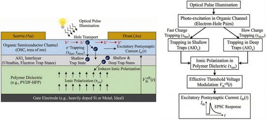
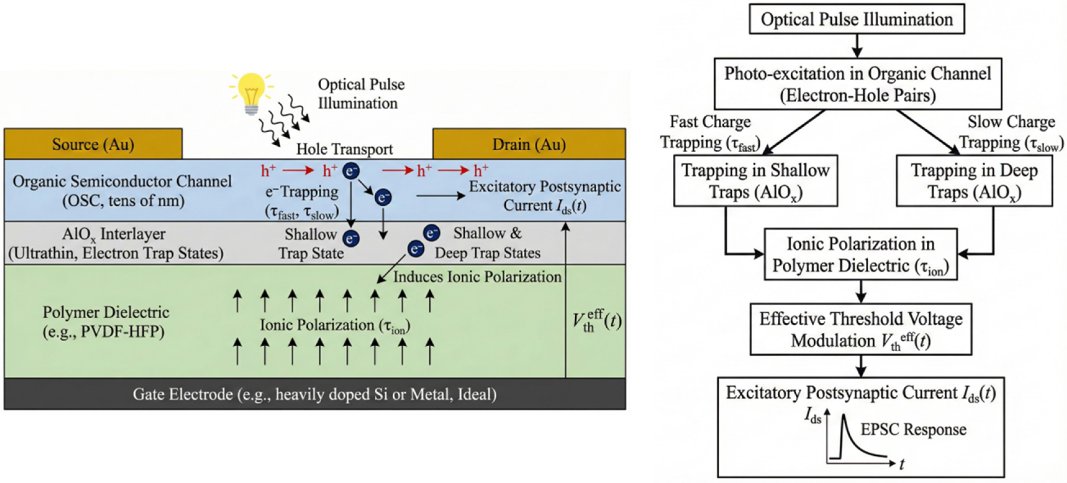
Figure 1 schematically illustrates the device structure and the physical mechanism underlying the optical synaptic behavior of the polymer-based transistor. The device adopts a bottom-gate, top-contact architecture, in which gold source and drain electrodes (Sigma-Aldrich, St. Louis, MO, USA) are deposited on an organic semiconductor (DPP-based polymer, Merck, Darmstadt, Germany) channel with a thickness of several tens of nanometers. Beneath the organic channel lies an ultrathin AlOx interlayer (ALD process, Kurt J. Lesker Company, Jefferson Hills, PA, USA) that serves as an electron trapping layer with abundant shallow and deep trap states, followed by a thick polymer dielectric layer exhibiting pronounced ionic polarization. The bottom gate electrode is treated as an ideal conductor in the model.
Figure 1.
Device structure and unified physical mechanism of the optical synaptic transistor based on coupled trap and ionic dynamics.
Upon optical pulse illumination, photo-excitation in the organic semiconductor generates electron–hole pairs. Owing to the energy landscape and interfacial properties, photogenerated holes remain mobile within the organic channel and contribute directly to lateral charge transport between the source and drain electrodes, forming the channel current. In contrast, photogenerated electrons are preferentially driven toward the AlOx interlayer and become trapped in shallow and deep interfacial states, characterized by fast and slow trapping time constants, respectively. The accumulation of trapped electrons produces an internal electric field that induces ionic polarization within the polymer dielectric on a slower time scale, denoted by .
The coupled dynamics of electron trapping and ionic polarization result in a time-dependent modulation of the effective threshold voltage , which in turn governs the evolution of the drain current. This dynamic threshold-voltage modulation gives rise to excitatory postsynaptic current responses under optical stimulation, as schematically summarized by the physical mechanism flow shown in Figure 1. Together, the device schematic and the mechanism flow illustrate how microscopic carrier and ionic dynamics are translated into macroscopic synaptic functions in the optical synaptic transistor.
2.2. Modeling of Trap–Ion Coupling in Optical Synaptic Transistors
Based on the physical picture illustrated in Figure 1, we model the optical synaptic behavior of the device by focusing on two dominant processes: photo-induced electron trapping at the semiconductor–dielectric interface and ionic polarization within the polymer dielectric [2,12,20]. These two processes operate on distinct time scales but jointly modulate the effective threshold voltage of the transistor channel. Secondary effects, such as contact resistance variation and drain-induced barrier lowering, are neglected to highlight the essential physics governing the synaptic response.
Under optical pulse illumination, electron–hole pairs are generated in the organic semiconductor channel [6,7,12]. Owing to the p-type transport nature and interfacial energy alignment, photogenerated holes remain mobile and contribute directly to the channel current, whereas photogenerated electrons are preferentially transferred to the AlOx interlayer and captured by interfacial trap states. To capture the experimentally observed fast and slow synaptic responses, the traps are divided into shallow and deep states, characterized by distinct trapping–detrapping time constants. The optical intensity is treated as an effective source term that accounts for photocarrier generation and transport without explicitly resolving spatial carrier dynamics [1].
In parallel with electron trapping, the accumulated interfacial charge produces an internal electric field that drives slow ionic redistribution in the polymer dielectric [17,18,19]. Owing to the low ionic mobility in polymer matrices, this ionic polarization is described as a slow relaxation process with a characteristic time constant τ_ion, typically longer than the electronic trapping time scales.
Rather than modifying the channel transport model for each microscopic process separately, their combined influence is incorporated through a time-dependent effective threshold voltage, . Both trapped charge and ionic polarization shift the threshold voltage via capacitive coupling to the channel, thereby directly controlling the drain current under a constant gate bias. As a result, excitatory postsynaptic current responses emerge naturally from the temporal evolution of , without introducing additional phenomenological synaptic elements. This unified modeling strategy establishes a direct and physically intuitive connection between microscopic carrier and ionic dynamics and macroscopic synaptic behavior [12,20,21,22].
2.3. Device Fabrication and Structure of Optical Synaptic Transistors
Optical synaptic transistors were fabricated in a bottom-gate, top-contact configuration on heavily doped Si substrates with a thermally grown SiO2 layer (≈300 nm) serving as the gate dielectric [11,20]. The substrates were sequentially cleaned by ultrasonication in acetone, isopropyl alcohol, and deionized water, followed by nitrogen drying and oxygen plasma treatment. A polymer dielectric layer was prepared by solution processing and spin-coated onto the substrates, followed by thermal annealing to remove residual solvent [6,7,20].
Subsequently, a diketopyrrolopyrrole (DPP)-based polymer semiconductor was deposited by spin coating from solution to form the active channel layer, and the resulting film was thermally annealed to optimize molecular packing and charge transport properties. A thin aluminum oxide (AlOx) interfacial layer was then introduced by low-temperature deposition to modulate the interfacial trap landscape and ion-related dynamics. Gold source and drain electrodes (≈40 nm) were thermally evaporated through a shadow mask, defining a channel length L and width W.
Electrical and optical synaptic measurements were carried out under ambient conditions using a semiconductor parameter analyzer (Keithley 4200-SCS, Tektronix, Inc., Beaverton, OR, USA). Optical stimuli were provided by a light-emitting diode China driven by a programmable function generator. The excitatory postsynaptic current (EPSC) was defined as the transient increase in drain current induced by an optical pulse under constant bias conditions. Paired-pulse facilitation (PPF) was measured by applying two consecutive light pulses separated by a variable inter-pulse interval Δt, while long-term synaptic behavior was evaluated by applying a train of identical optical pulses and monitoring the evolution of EPSC peak values. Experimentally extracted EPSC peaks were further normalized and analyzed as effective synaptic weight variables for comparison with the proposed physical model.
3. Unified Trap–Ion Dynamic Model
3.1. Photo-Induced Charge Trapping Dynamics
Spatial carrier transport is not explicitly resolved, as the focus of the present model is on temporal dynamics rather than spatial inhomogeneity. Under optical pulse illumination, electron–hole pairs are generated in the organic semiconductor channel [6,7,12]. Owing to the p-type transport nature and the interfacial energy alignment, photogenerated holes remain mobile and contribute directly to channel conduction, whereas photogenerated electrons are preferentially transferred toward the semiconductor–dielectric interface and captured by trap states in the ultrathin AlOx interlayer.
To describe the coexistence of fast and slow synaptic responses, the interfacial trap states are divided into shallow and deep traps [12,13]. The time evolution of the trapped electron densities is governed by:
where and denote the surface densities of electrons trapped in shallow and deep states, respectively; represents the normalized optical excitation intensity; and are the corresponding trapping coefficients; and and are the characteristic trapping–detrapping time constants [2,12].
3.2. Ionic Polarization Dynamics in Polymer Dielectric
The accumulation of trapped electrons at the AlOx_interface generates an internal electric field that penetrates into the polymer dielectric layer and drives the redistribution of mobile ions [17,20]. Owing to the intrinsically low ionic mobility in polymer matrices, the ionic response occurs on a much longer time scale than electronic trapping and is therefore treated as a slow relaxation process [18,19,20].
The temporal evolution of the ionic polarization charge density is described by
where is the coupling coefficient between the gate electric field and ionic displacement, is the applied gate voltage, and is the ionic relaxation time constant [2,17,20]. Here, the gate voltage is introduced as an effective driving term for ionic polarization rather than a spatially resolved electric field. This formulation represents a coarse-grained, mean-field description in which the net electrostatic force acting on mobile ions arises from both the externally applied gate bias and the internal electric field induced by trapped interfacial charges. Spatial variations of the electric field across the dielectric and their dependence on are not explicitly resolved, but are effectively absorbed into the ionic coupling coefficient kion, which accounts for dielectric thickness, permittivity, ionic mobility, and local field redistribution.
3.3. Time-Dependent Effective Threshold Voltage
Rather than modifying the channel transport equation for each microscopic process separately, the combined effects of charge trapping and ionic polarization are incorporated through a time-dependent effective threshold voltage [11,12,21,22]. Within the framework of field-effect transistors, these effects naturally manifest as a shift in the threshold voltage. The effective threshold voltage is expressed as
where is the intrinsic threshold voltage in the absence of optical stimulation and is the areal capacitance of the gate dielectric stack [11,12]. Equation (4) represents a first-order approximation valid in the non-saturated operating regime, where the accumulated trapped charge remains below the level at which strong electrostatic screening or capacitance nonlinearity becomes dominant. In this regime, the threshold-voltage shift scales approximately linearly with the total effective charge, and the gate dielectric stack can be described by an effective capacitance. At very high trapped charge densities or under prolonged strong stimulation, nonlinear electrostatic effects may lead to deviations from linear superposition, which are beyond the scope of the present unified model.
3.4. Drain Current and EPSC Response
For a p-type organic transistor operating in the saturation regime under a constant drain bias [11,12], the drain current can be written as
where and are the channel width and length, respectively, and is the effective hole mobility. Under optical pulse stimulation, the temporal evolution of directly modulates the channel conductance, giving rise to the observed excitatory postsynaptic current responses [1,6,8].
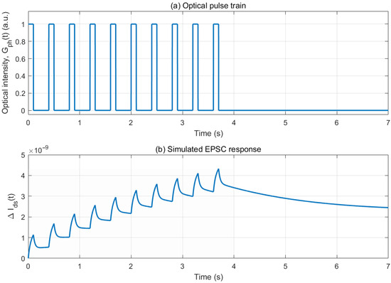
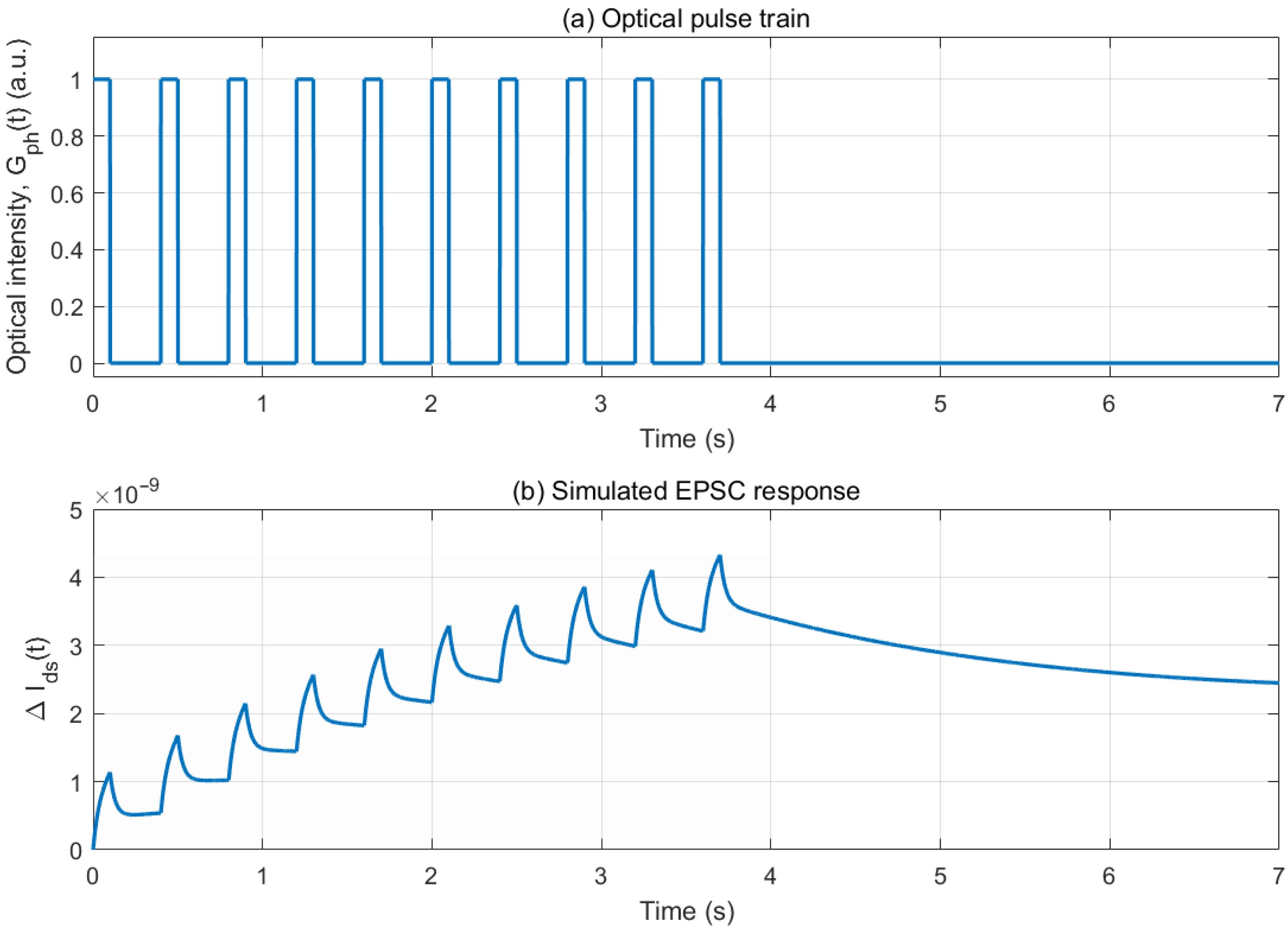
As shown in Figure 2, the simulated EPSC exhibits an initial rapid increase followed by a gradual saturation under repeated optical stimulation, capturing the essential features of synaptic potentiation. Notably, the non-uniform growth rate suggests the coexistence of multiple characteristic time scales, which will be analyzed in detail in the following section [1,6,8,11,12].
Figure 2.
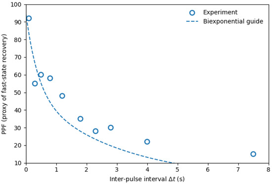
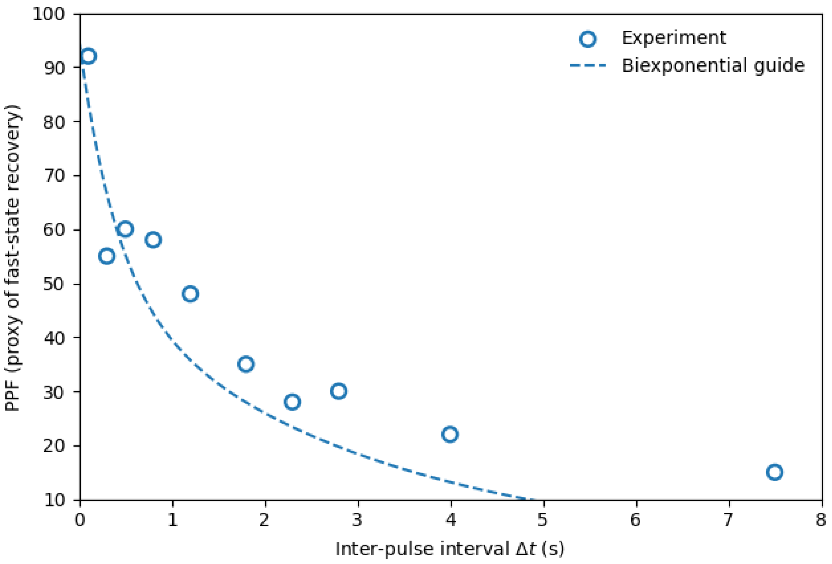
Paired-pulse facilitation (PPF) as a function of inter-pulse interval Δt. PPF is used here as an experimental proxy of fast-state recovery between successive stimuli. The dashed line represents a biexponential relaxation behavior and is shown as a guide to illustrate the presence of multiple fast recovery time scales.
3.5. Physical Origin of Multi-Timescale Synaptic Plasticity
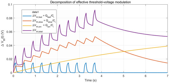
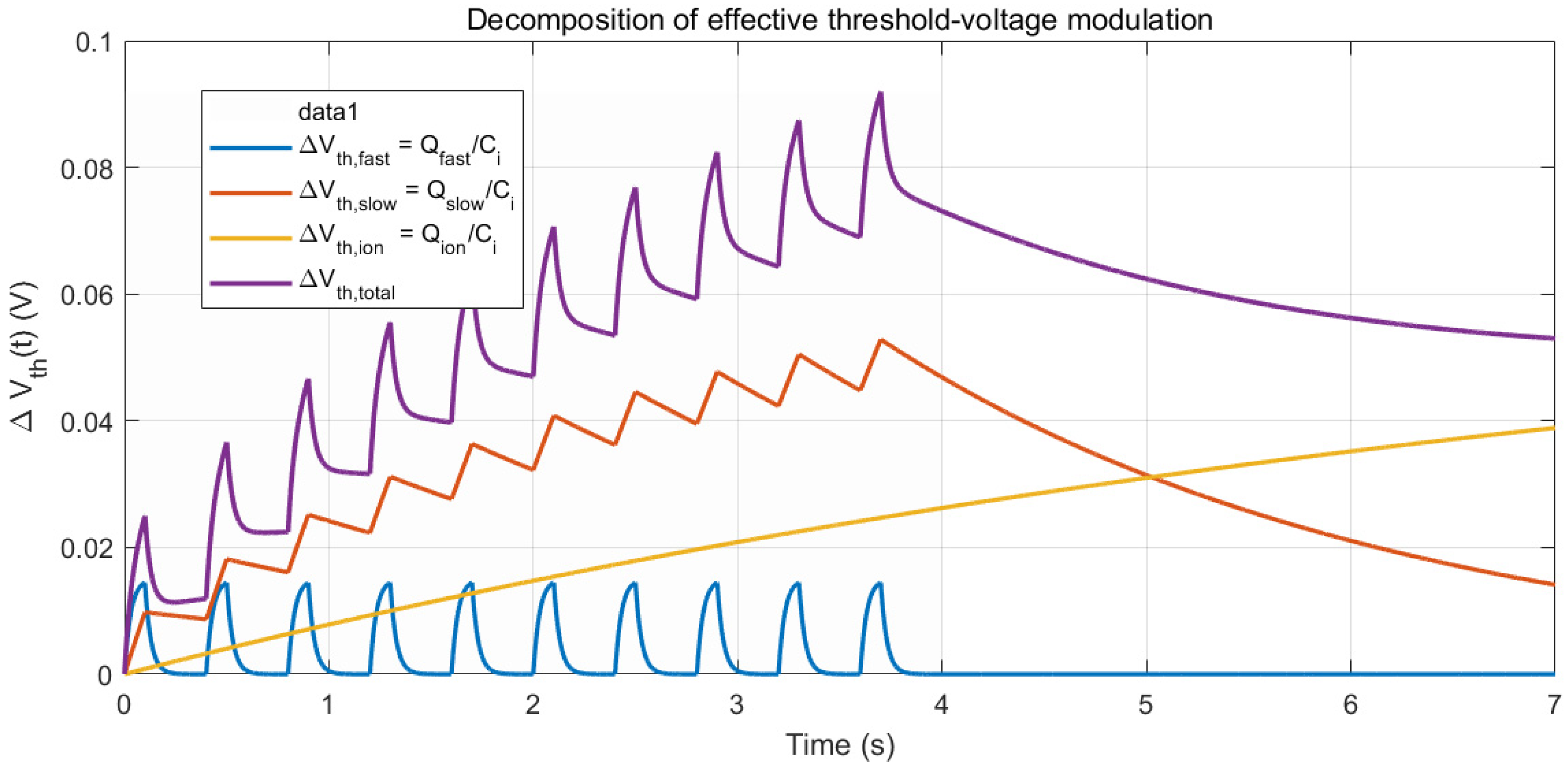
Within the unified trap–ion dynamic framework, the emergence of multi-timescale synaptic plasticity can be directly understood from the distinct temporal evolutions of the fast trapping, slow trapping, and ionic polarization processes, as explicitly illustrated in Figure 3. As shown in Figure 3, the shallow-trap-related contribution exhibits a rapid rise and decay synchronized with each optical pulse, reflecting the fast trapping–detrapping dynamics characterized by the time constant τ_fast. This component dominates the instantaneous enhancement of the drain current during illumination and is responsible for the transient EPSC peaks observed during optical stimulation [8,12]. Owing to its short relaxation time, the fast-trap contribution does not accumulate significantly over successive pulses and therefore primarily governs short-term plasticity [8].
Figure 3.
Simulated EPSC behavior under repetitive optical stimulation. (a) Schematic optical pulse sequence used as the excitation input in the model. (b) Time evolution of the incremental drain current ΔIds(t) calculated from the coupled trap–ion dynamic equations. The stepwise enhancement of the current during optical stimulation and its gradual relaxation afterward originate from the interplay between fast charge trapping, slow deep trapping, and ionic polarization, demonstrating the emergence of multi-timescale synaptic plasticity.
In contrast, the deep-trap-related contribution evolves on a much longer time scale defined by τ_slow. During repetitive optical stimulation, deep traps gradually accumulate charge, leading to a progressive shift of the effective threshold voltage and a stepwise elevation of the EPSC baseline. After termination of the optical pulses, this component relaxes slowly, giving rise to intermediate-term memory effects [12,19].
The ionic polarization component displays the slowest temporal response, with a characteristic relaxation time τ_ion that exceeds both electronic trapping time scales. As a result, the ionic contribution increases almost monotonically during stimulation and remains substantial long after the optical pulses are switched off. This slow ionic relaxation dominates the long retention behavior and provides the physical origin of long-term potentiation in the device [2,20].
Importantly, Figure 3 reveals that the observed EPSC evolution is not governed by a single effective time constant, but rather arises from a sequential dominance of different physical processes at different stages of stimulation and relaxation [1,8]. During each optical pulse, fast electronic trapping controls the instantaneous EPSC response; over repeated pulses, deep trapping progressively modulates the baseline conductance; and after pulse termination, ionic polarization dictates the long-term decay dynamics [8,12,20]. The transition from short-term to long-term plasticity is therefore determined by the competition between the optical pulse interval and the intrinsic relaxation time constants τ_fast, τ_slow, and τ_ion [1].
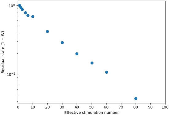
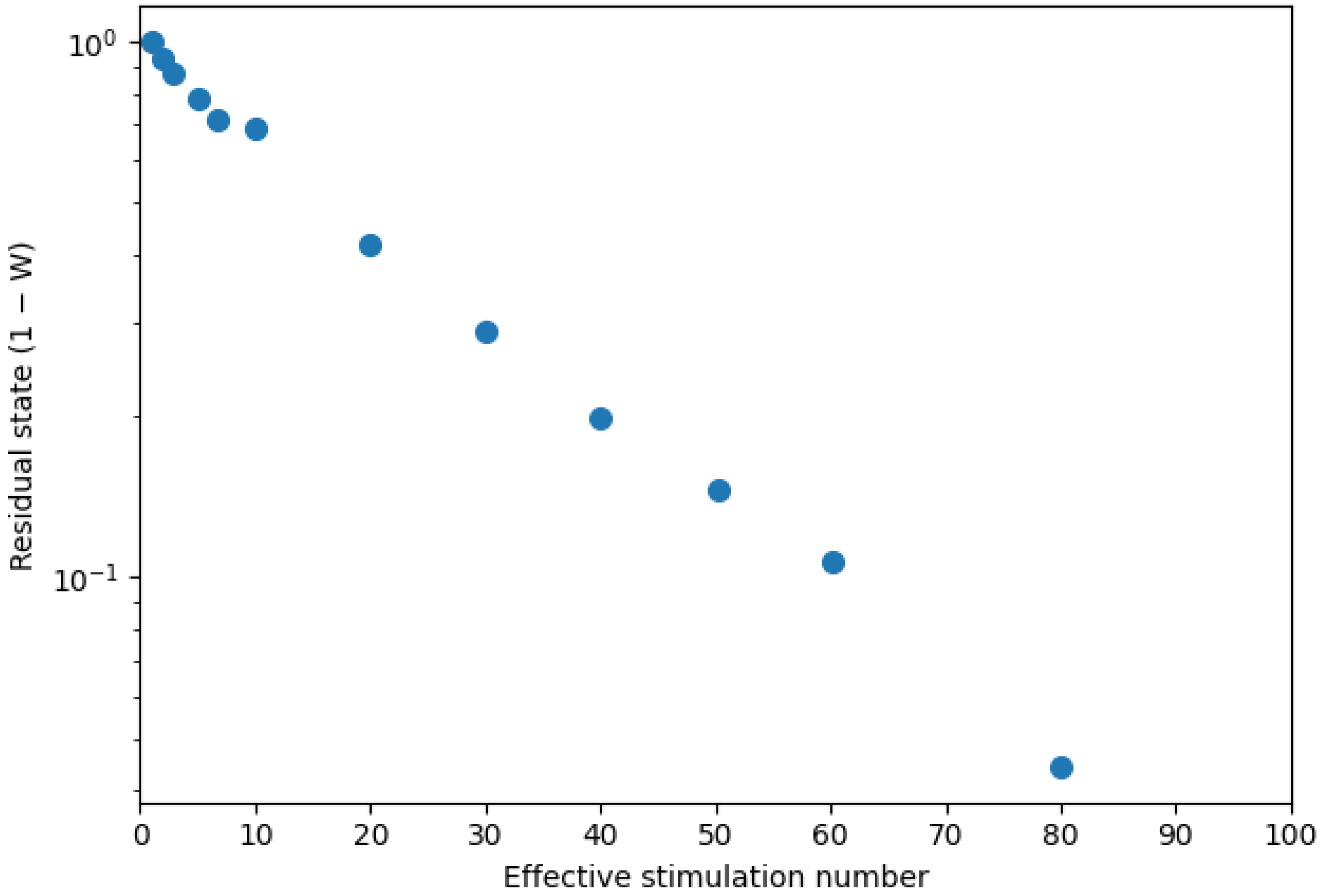
This decomposition provides a physically transparent interpretation of the EPSC behavior shown in Figure 3 and highlights how multi-timescale synaptic plasticity naturally emerges from the coupled trap–ion dynamics, as further clarified by the component-resolved analysis in Figure 4, without invoking phenomenological synaptic rules [1,21,22]. It should be emphasized that the simulated EPSC responses in Figure 3 are not intended to reproduce specific experimental current magnitudes. Instead, they are used to demonstrate that the proposed physical model captures the essential synaptic behaviors observed in optical synaptic transistors, including short-term plasticity, long-term potentiation, and their evolution under repetitive optical stimulation [6,7]. This explicit decomposition clarifies the respective roles of electronic and ionic processes, which are often difficult to disentangle experimentally [1]. In addition to the time-domain EPSC evolution, the relaxation behavior of the residual synaptic state provides further insight into the underlying slow internal dynamics. As shown in Figure 5, the residual synaptic state, defined as 1 − W, exhibits an approximately linear decay on a semi-logarithmic scale as a function of effective stimulation number. This behavior is characteristic of a first-order relaxation process, indicating a gradual depletion of available slow internal states, such as deep traps or slowly relaxing ionic polarization, under repeated optical stimulation. The observed trend is therefore consistent with the model assumption that long-term synaptic retention is governed by slow, cumulative processes rather than fast transient trapping.
Figure 4.
Decomposition of trap and ionic contributions in the unified model. Time evolution of the (shallow) fast-trap charge , (deep) slow-trap charge , and ionic polarization charge (or equivalently their contributions to ). The fast component governs the rapid EPSC transients within each pulse, whereas the slow trap and ionic polarization components accumulate over repeated stimulation and dominate the long retention behavior after pulse termination. The pulse interval shown here exceeds the shallow-trap detrapping time τ_fast and is chosen as a representative condition to highlight the intrinsic separation of time scales. For shorter pulse intervals comparable to or below τ_fast, the fast-trap contribution becomes partially accumulative, which is naturally captured by the same model through its characteristic time constants.
Figure 5.
Semi-logarithmic plot of the residual synaptic state as a function of effective stimulation number. The residual state is defined as , where is the normalized synaptic weight extracted from the EPSC peak. The approximately linear decay indicates a first-order relaxation process associated with the gradual depletion of available slow internal states under repeated stimulation.
4. Model Parameters and Simulation Conditions
4.1. Device Geometry and Material Parameters
The key device and model parameters used in the simulations are summarized in Table 1. The numerical simulations are based on a device structure representative of polymer-based optical synaptic transistors widely reported in the literature [1,6,7]. The transistor adopts a bottom-gate, top-contact configuration, consisting of an organic semiconductor (OSC) channel contacted by Au source and drain electrodes, an ultrathin AlOx_interlayer acting as an electron trapping layer, and a thick polymer dielectric layer exhibiting pronounced ionic polarization [11,12,20]. The gate electrode is assumed to be heavily doped Si or patterned metal with a thickness of 100–150 nm and is treated as an ideal conductor in the model, as the gate material does not affect the time-dependent synaptic dynamics considered here [11].
Table 1.
Model parameters used in simulations.
The polymer dielectric layer (e.g., PVDF-HFP) has a thickness of 300–600 nm and a relative dielectric constant ≈ 7–10 [17,18,20]. The ionic mobility in the polymer matrix is taken to be in the range of 10−12–10−10, resulting in a gate areal capacitance ≈ 4 × 10⁻⁵–8 × 10⁻⁵ F m−2 [18,20]. An ultrathin AlOx, interlayer with a thickness of 2–5 nm is inserted between the OSC and the polymer dielectric, providing a high density of interfacial electron trap states (1012–1013 cm−2) [12,14,15]. Both shallow and deep traps are considered to account for the experimentally observed coexistence of fast and slow synaptic responses, with characteristic trapping time constants of ≈ 10–100 ms ≈ 0.5–5 s, respectively [12,13].
The organic semiconductor channel has a thickness of 30–80 nm and an effective hole mobility in the range of 0.1–1 cm2V−1s−1, corresponding to 1 × 10⁻⁵–1 × 10⁻⁴ m2V−1s−1 in SI units [9,10,11,12]. The channel length and width are chosen to be L = 50–300 μm and W = 1–5 mm, respectively. A large W/L ratio is employed to enhance the drain current and facilitate the observation of synaptic responses [11].
4.2. Optical Stimulation Conditions and Simulation Setup
Optical stimulation is applied in the form of a train of identical light pulses with pulse widths of 50–200 ms and pulse intervals of 200–500 ms [6,7,8]. The illumination wavelength is selected within the range of 365–520 nm, depending on the absorption characteristics of the OSC, while the optical power density is treated as a normalized quantity (0–1 a.u.) in the simulations [6,7]. All device and model parameters, including trapping coefficients, ionic relaxation times, and threshold-voltage shifts, are chosen within physically reasonable and experimentally relevant ranges. This ensures that the simulated current levels and time constants are consistent with reported polymer-based optical synaptic transistors [1,6,7]. Importantly, instead of introducing an abstract synaptic weight or phenomenological conductance kernel, the model adopts a threshold-voltage-based description that naturally links microscopic interfacial charge and ionic processes to macroscopic channel transport [1,11,12].
While additional microscopic effects may contribute in specific material systems, the present model focuses on the dominant processes governing the hierarchy of synaptic time scales, thereby providing a minimal yet physically transparent framework for understanding optical synaptic dynamics [1,20].
5. Conclusions
In this work, we have developed a unified physical model to describe the optical synaptic behaviors of polymer-based organic transistors by explicitly coupling photo-induced charge trapping and ionic polarization dynamics. By incorporating fast and slow electron trapping at the semiconductor–dielectric interface together with the slow ionic response in the polymer dielectric, the model provides a self-consistent description of the time-dependent threshold-voltage modulation that governs the channel conductance under optical stimulation.
The proposed framework successfully reproduces key synaptic functions observed in optical synaptic transistors, including excitatory postsynaptic current (EPSC), short-term plasticity, long-term potentiation, and their evolution under repetitive optical pulse excitation. Importantly, the model reveals that multi-timescale synaptic plasticity does not originate from a single effective relaxation process, but instead arises from the sequential dominance of fast trapping, deep trapping, and ionic polarization, each characterized by distinct intrinsic time constants [21,22].
By explicitly decomposing the contributions of electronic trapping and ionic polarization to the effective threshold voltage, the model offers clear physical insight into the respective roles of fast and slow processes that are often difficult to disentangle experimentally. This decomposition establishes a transparent link between microscopic interfacial charge dynamics and macroscopic synaptic responses, enabling a unified interpretation of transient and long-retention memory behaviors within a single device framework.
Beyond reproducing reported synaptic phenomena, the proposed framework offers practical guidance for tuning synaptic time scales through material and structural design, enabling the rational optimization of polymer-based neuromorphic devices toward targeted short-term or long-term memory functions. The modeling approach is general and can be readily extended to other hybrid ion–electronic synaptic systems, such as electrolyte-gated transistors and floating-gate phototransistors [23,24,25].
Overall, this work establishes a physically intuitive and experimentally relevant modeling platform for understanding and designing optical synaptic transistors, and is expected to facilitate the systematic development of polymer-based neuromorphic computing hardware [24,25,26,27,28].
Author Contributions
Conceptualization, Y.W.; methodology, Y.W.; software, J.H.; validation, Y.W. and J.H.; formal analysis, Y.W.; investigation, J.H.; resources, Y.W.; data curation, J.H.; writing—original draft preparation, J.H.; writing—review and editing, Y.W.; visualization, J.H.; supervision, Y.W.; project administration, Y.W.; funding acquisition, Y.W. All authors have read and agreed to the published version of the manuscript.
Funding
This research was funded by the National Natural Science Foundation of China (Grant No. 52507281) and the Young Doctor Program of Xinqiao Hospital (Grant No. 048).
Institutional Review Board Statement
Not applicable.
Informed Consent Statement
Not applicable.
Data Availability Statement
The original contributions presented in this study are included in the article. Further inquiries can be directed to the corresponding author.
Conflicts of Interest
The authors declare no conflict of interest.
References
- van De Burgt, Y.; Melianas, A.; Keene, S.T.; Malliaras, G.; Salleo, A. Organic electronics for neuromorphic computing. Nat. Electron. 2018, 1, 386–397. [Google Scholar] [CrossRef] [Scilit]
- Gkoupidenis, P.; Schaefer, N.; Garlan, B.; Malliaras, G.G. Neuromorphic functions in PEDOT: PSS organic electrochemical transistors. Adv. Mater. 2015, 27, 7176–7180. [Google Scholar] [CrossRef] [Scilit] [PubMed]
- Indiveri, G.; Liu, S.C. Memory and information processing in neuromorphic systems. Proc. IEEE 2015, 103, 1379–1397. [Google Scholar] [CrossRef] [Scilit]
- Mead, C. Neuromorphic electronic systems. Proc. IEEE 2002, 78, 1629–1636. [Google Scholar] [CrossRef] [Scilit]
- Yang, J.J.; Strukov, D.B.; Stewart, D.R. Memristive devices for computing. Nat. Nanotechnol. 2013, 8, 13–24. [Google Scholar] [CrossRef] [Scilit]
- Li, Q.; Wang, T.; Hu, X.; Wu, X.; Zhu, H.; Ji, L.; Sun, Q.; Zhang, D.W.; Chen, L. Organic optoelectronic synaptic devices for energy-efficient neuromorphic computing. IEEE Electron. Device Lett. 2022, 43, 1089–1092. [Google Scholar] [CrossRef] [Scilit]
- Zhao, P.; Peng, X.; Cui, M.; Li, Y.; Jiang, C.; Luo, C.; Tian, B.; Lin, H.; Peng, H.; Duan, C.-G. Multifunctional two-terminal optoelectronic synapse based on an organic semiconductor film. ACS Appl. Polym. Mater. 2023, 5, 8764–8773. [Google Scholar] [CrossRef] [Scilit]
- Ohno, T.; Hasegawa, T.; Tsuruoka, T.; Terabe, K.; Gimzewski, J.K.; Aono, M. Short-term plasticity and long-term potentiation mimicked in single inorganic synapses. Nat. Mater. 2011, 10, 591–595. [Google Scholar] [CrossRef] [Scilit]
- Bronstein, H.; Nielsen, C.B.; Schroeder, B.C.; McCulloch, I. The role of chemical design in the performance of organic semiconductors. Nat. Rev. Chem. 2020, 4, 66–77. [Google Scholar] [CrossRef] [Scilit]
- Liang, Y.; Yu, L. A new class of semiconducting polymers for bulk heterojunction solar cells with exceptionally high performance. Acc. Chem. Res. 2010, 43, 1227–1236. [Google Scholar] [CrossRef] [Scilit] [PubMed]
- Sirringhaus, H. 25th anniversary article: Organic field-effect transistors: The path beyond amorphous silicon. Adv. Mater. 2014, 26, 1319–1335. [Google Scholar] [CrossRef] [Scilit] [PubMed]
- Salleo, A. Charge transport in polymeric transistors. Mater. Today 2007, 10, 38–45. [Google Scholar] [CrossRef] [Scilit]
- Kim, S.; Yoo, H.; Choi, J. Effects of charge traps on hysteresis in organic field-effect transistors and their charge trap cause analysis through causal inference techniques. Sensors 2023, 23, 2265. [Google Scholar] [CrossRef] [Scilit]
- Jeong, Y.; Bae, C.; Kim, D.; Song, K.; Woo, K.; Shin, H.; Cao, G.; Moon, J. Bias-stress-stable solution-processed oxide thin film transistors. ACS Appl. Mater. Interfaces 2010, 2, 611–615. [Google Scholar] [CrossRef] [Scilit]
- Kim, M.G.; Kanatzidis, M.G.; Facchetti, A.; Marks, T.J. Low-temperature fabrication of high-performance metal oxide thin-film electronics via combustion processing. Nat. Mater. 2011, 10, 382–388. [Google Scholar] [CrossRef] [Scilit]
- Bhadra, R.; Kumar, R.; Kumar, A. Device Engineering of Dual Metal Gate-Based Artificial Synapse for Enhanced Plasticity Utilizing Al2O3-Based Ion Conducting Electrolyte. IEEE Trans. Electron. Devices 2024, 71, 2749–2754. [Google Scholar] [CrossRef] [Scilit]
- Tsutsumi, N.; Bai, X.; Sakai, W. Towards nonvolatile memory devices based on ferroelectric polymers. AIP Adv. 2012, 2, 012154. [Google Scholar] [CrossRef] [Scilit]
- Hanna, A.N.; Bhansali, U.S.; Khan, M.A.; Alshareef, H. Characterization of current transport in ferroelectric polymer devices. Org. Electron. 2014, 15, 22–28. [Google Scholar] [CrossRef] [Scilit]
- Kim, J.H.; Halaksa, R.; Jo, I.Y.; Ahn, H.; Gilhooly-Finn, P.A.; Lee, I.; Park, S.; Nielsen, C.B.; Yoon, M.-H. Peculiar transient behaviors of organic electrochemical transistors governed by ion injection directionality. Nat. Commun. 2023, 14, 7577. [Google Scholar] [CrossRef] [Scilit]
- Rivnay, J.; Inal, S.; Salleo, A.; Owens, R.M.; Berggren, M.; Malliaras, G.G. Organic electrochemical transistors. Nat. Rev. Mater. 2018, 3, 17086. [Google Scholar] [CrossRef] [Scilit]
- Chua, L. Memristor-the missing circuit element. IEEE Trans. Circuit Theory 2003, 18, 507–519. [Google Scholar] [CrossRef] [Scilit]
- Strukov, D.B.; Snider, G.S.; Stewart, D.R.; Williams, R.S. The missing memristor found. Nature 2008, 453, 80–83. [Google Scholar] [CrossRef] [Scilit] [PubMed]
- Zahoor, F.; Bature, U.I.; Nisar, A.; Alzahrani, A.; Abbas, H.; Bashir, F. A Comprehensive Review on Physical Unclonable Functions Based on Resistive Random Access Memory. ACS Appl. Electron. Mater. 2025, 7, 6215–6242. [Google Scholar] [CrossRef] [Scilit]
- Sahu, M.C.; Jena, A.K.; Mallik, S.K.; Roy, S.; Sahoo, S.; Ajimsha, R.S.; Misra, P.; Sahoo, S. Reconfigurable low-power TiO2 memristor for integration of artificial synapse and nociceptor. ACS Appl. Mater. Interfaces 2023, 15, 25713–25725. [Google Scholar] [CrossRef] [Scilit]
- Hwang, S.I.; Cho, H.Y.; Yoon, J.H. Multi-timescale temporal processing for ion-motion memristor-based physical reservoir computing. Device 2025, 3, 100907. [Google Scholar] [CrossRef] [Scilit]
- Yang, C.S.; Shang, D.S.; Liu, N.; Fuller, E.J.; Agrawal, S.; Talin, A.A.; Li, Y.Q.; Shen, B.G.; Sun, Y. All-solid-state synaptic transistor with ultralow conductance for neuromorphic computing. Adv. Funct. Mater. 2018, 28, 1804170. [Google Scholar] [CrossRef] [Scilit]
- Kim, K.N.; Sung, M.J.; Park, H.L.; Lee, T. Organic synaptic transistors for bio-hybrid neuromorphic electronics. Adv. Electron. Mater. 2022, 8, 2100935. [Google Scholar] [CrossRef] [Scilit]
- Berggren, M.; Crispin, X.; Fabiano, S.; Jonsson, M.P.; Simon, D.T.; Stavrinidou, E.; Tybrandt, K.; Zozoulenko, I. Ion electron–coupled functionality in materials and devices based on conjugated polymers. Adv. Mater. 2019, 31, 1805813. [Google Scholar] [CrossRef] [Scilit]

Disclaimer/Publisher’s Note: The statements, opinions and data contained in all publications are solely those of the individual author(s) and contributor(s) and not of MDPI and/or the editor(s). MDPI and/or the editor(s) disclaim responsibility for any injury to people or property resulting from any ideas, methods, instructions or products referred to in the content. |
© 2026 by the authors. Licensee MDPI, Basel, Switzerland. This article is an open access article distributed under the terms and conditions of the Creative Commons Attribution (CC BY) license.