


Abstract
Background: The optical losses in the form of reflections, parasitic absorption, and scattering limit photovoltaic efficiency. This review examines plasma-assisted surface engineering as an effective tool for improving light management in solar cells. Plasma-based methods, including etching, oxidation, deposition, and texturing, enable precise control of surface morphology and chemistry, lowering reflectance, enhancing light trapping, and passivating defects. Methods: In contrast to wet-chemical or high-temperature processes, plasma processes are dry, low-temperature, scalable, and can be used with silicon, perovskite, thin-film, and organic solar cells, as well as tandem structures. The fundamentals of optical losses are described, along with the principles of radio-frequency (RF), inductively coupled plasma (ICP), microwave, and atmospheric plasma systems and their distinctive advantages for controlling ion and reactive-species generation. Key applications reviewed include black-silicon texturing by ICP reactive-ion etching (ICP-RIE), anti-reflective/passivation coatings by plasma-enhanced chemical vapor deposition (PECVD), and interface activation by atmospheric plasma. Results: Among performance improvements are a reflectance of less than 2%, a photocurrent increase of 10–20%, and longer carrier lifetime. Conclusions: The advantages of plasma compared to lithography and sol–gel processes are in the precision and affordability of the method. The difficulties include damage caused by the processing, uniformity over extensive areas, and environmental stress resistance. Future directions rely on low-temperature plasmas for flexible PV, machine-learning-guided process optimization, and hybrid plasma–laser systems. This synthesis of otherwise fragmented studies is intended to support the implementation of plasma-based methods in next-generation, high-efficiency, and sustainable solar production.
1. Introduction
The current fast-paced shift to sustainable energy systems at the global scale has fueled interest in photovoltaic (PV) technologies that can address the long-term energy requirements of the global population [1]. Beyond electricity generation, solar-driven technologies are also being extended to applications such as photothermal water purification, underscoring the breadth of solar energy’s role in addressing global sustainability challenges [2]. With the rapid use of solar energy in the industrial, commercial, and utility-scale sectors, there is a strategic move to enhance the efficiency of the devices used and also minimize the manufacturing cost [3]. Nevertheless, despite the achievement of significant advancements in materials, interfaces, and device architectures, solar cells still experience the classical efficiency constraints due to optical losses, which include reflection at the front surface, insufficient light trapping, parasitic absorption, and incomplete photon utilization [4]. All these losses add up to limit the quantity of incident sunlight that can be reasonably converted to electrical energy.
In order to address these bottlenecks, progressive methods of light management have grown as performance enhancers in recent photovoltaic research [5]. These strategies have the potential to maximize optical path length, reduce reflection, and enhance intense absorption of photons by a solar cell by optimizing the light-surface or interface interaction. Surface engineering has a key role in this process since the morphology, chemical composition, and texture of the surface of the solar cell have a significant impact on the optical behavior and electrical characteristics [6,7].
Plasma-assisted processes are some of the different surface modification methods, which have gained increasing popularity with regard to their accuracy, control, and the ability to apply the technique across diverse photovoltaic materials [8,9]. Plasma etching, plasma oxidation, plasma-enhanced deposition, and plasma-induced texturing enable micro-/nanoscale surface modifications with a high level of control, reducing reflectance, enhancing light trapping, tuning refractive indices, and passivating defects [10]. Unlike conventional wet-chemical or high-temperature treatments, plasma treatments are dry, low-temperature, and environmentally friendly, and are compatible with silicon, perovskite, thin-film, organic, and tandem solar cell architectures [11]. These attributes make plasma-assisted engineering very promising for use in the next generation of PV applications.
Although there is growing interest, the current literature is still divided into studies on individual processes in plasma, individual materials, or individual performance outcomes. This discontinuity produces a distinct research gap: the lack of a unified, methodical knowledge of the role of plasma-assisted surface engineering in increased light regulation in a wide range of photovoltaic designs. It is necessary to have an overall review that encompasses mechanisms and applications, performance measures, and comparison insights to drive future research and industry adoption.
This review distinguishes itself from existing review articles in several respects. Prior reviews have generally focused on individual plasma processes, such as etching or deposition alone [12,13], on a single photovoltaic material system, such as crystalline silicon passivation [14,15], or on a single device architecture; none provide a systematic, cross-architecture synthesis that spans silicon, perovskite, thin-film, organic, and tandem technologies within a single comparative framework. Rather than only describing reported plasma parameters and efficiencies, this review critically benchmarks plasma-based light management against a broad range of conventional and emerging alternatives, provides the first consolidated quantitative breakdown of optical losses across crystalline-silicon, perovskite, and tandem architectures [16,17], and explicitly discusses plasma-induced degradation mechanisms, ion-bombardment damage, defect formation, and surface roughening that are frequently omitted from process-focused reviews. It further extends the discussion to industrial scalability metrics (manufacturing cost, throughput, and large-area uniformity) and to emerging machine-learning-guided process optimization [18,19], both of which have received limited attention in the existing literature.
To meet this requirement, the current paper undergoes a critical review of the plasma-assisted surface engineering strategies to enhance light management in solar cells. It is hoped that recent advances will be synthesized, the effect they have on optical and electronic performance will be evaluated, and the methods of handling light using plasmas will be compared with other more advanced light-management techniques. The review provides evidence about the basic mechanisms, applications, and perspectives of plasma-assisted photovoltaic enhancement. In this review, several secondary sources such as Scopus, Web of Science, Springer, ScienceDirect, IEEE Xplore, DOAJ, and EBSCO have been searched to obtain the relevant data.
This review follows this structure: Section 2: The fundamentals of light management and the sources of optical loss that are critical in solar cells. Section 3 introduces the principles of the processes, mechanisms, and the nature of operation of the plasma-assisted processes. In Section 4, significant plasma-based surface modification methods and their functional implications in light trapping and interface engineering are reviewed. Section 5 examines how the concept of plasma-assisted engineering can be applied to various solar cell designs. Section 6 measures performance improvement and compares the plasma techniques to other light-management strategies. Section 7 will describe the emerging trends, existing limitations, and research gaps, whilst Section 8 will mention any prospects. Section 9 concludes the paper, summarizing key lessons and determining the future outlook of the subject of plasma-based surface engineering for photovoltaic technologies.
2. Fundamentals of Light Management in Solar Cells
2.1. Types of Optical Losses in Solar Cells
One of the most important aspects that restricts the efficiency of photovoltaic devices is optical losses [20]. Overall, the losses can be categorized into three primary categories, namely, reflection, parasitic absorption, and scattering losses [21]. The refractive index between the air and the semiconductor absorber does not match, which causes front-surface reflection. For materials with a high refractive index, such as crystalline silicon (n ≈ 3.5), reflection losses can exceed 30% even without anti-reflective measures [22]. Parasitic absorption is absorption in layers that do not play a role in electron-hole generation, e.g., transparent conductive oxides, metal contacts, buffer layers, or encapsulants [23]. This kind of absorption diminishes the number of photons at the active layer. Scattering and escape loss are caused by photons that get inside the device getting scattered out of the absorber, mostly in thin-film solar cells, where the absorber thickness is less than the optical penetration depth [24]. The loss of angular momentum and the buildup of light in non-absorbing areas also contribute to low photocurrent.
To contextualize the severity of these losses, quantitative breakdowns for mainstream photovoltaic technologies are instructive. In crystalline silicon solar cells without anti-reflection measures, front-surface reflection alone accounts for approximately 30–35% of incident AM1.5G sunlight in the 300–1100 nm spectral range, while parasitic absorption in metal contacts and transparent conductive oxide (TCO) layers contributes approximately 5–10% additional losses, and scattering/escape losses are typically 3–5% for optimized surface textures [16,22]. With state-of-the-art light trapping that combines textured (e.g., black silicon) surfaces with anti-reflective coatings, total optical losses in high-efficiency c-Si cells can be reduced to roughly 5–10%, comprising reflection below 3%, parasitic absorption of approximately 4%, and scattering of approximately 2% [16]. In perovskite solar cells, the optical loss budget is distributed differently owing to the thinner absorber layers: reflection losses account for approximately 10–15% depending on the top-contact design, parasitic absorption in the hole-transport layer (e.g., spiro-OMeTAD) contributes approximately 8–12%, and scattering losses in polycrystalline perovskite films can reach 5–10% due to grain-boundary scattering [16]. In perovskite/silicon tandem configurations, interlayer parasitic absorption of approximately 3–5% per interface is typically observed; nevertheless, optimized cell-to-module integration has been reported to yield active-area module efficiencies of up to 25.5% for one-cell and 24.6% for four-cell tandem mini-modules, illustrating how effective light management can suppress these cumulative losses [17]. These quantitative differences underscore the need for architecture-specific light-management strategies, which the remainder of this review addresses in detail.
Figure 1 depicts different plasmonic waveguide structures on a silver Bragg reflector (Ag BR) [25]. Panel (a) depicts the incident light (hν) on a silicon (Si) film, which supports guided modes with surface plasmon polariton (SPP) modes and ohmic loss at the Ag BR interface. In panel (b), an air gap has been drawn above the Si film, and incident light is scattered there, which favors guided and SPP modes with ohmic losses. In panel (c), a 3D model is used to showcase an array of silicon nanowires (Si NW) on an array of Ag nano-holes on the Ag BR. In panel (d), there is a unit cell having a circular feature of diameter a. A cross-section of a layer of Si (height L, pitch p) on Ag BR (thickness a) is shown in panel (e). In panel (f), a 3D schematic of a perfectly matched layer (PML) and perfectly matched conductor (PMC) boundary conditions, probe lines (AB), and areas (C) to analyze the field are shown, showing wavevector k and electric field E.
Figure 1.
Plasmonic waveguide structures on an Ag BR. (a) guided/SPP modes and ohmic losses in a flat Si film. (b) Enhanced scattering and losses due to an air gap above the Si film. (c) 3D model of a Si NW array on an Ag nanohole grating. (d,e) Top and cross-sectional views showing unit cell dimensions. (f) 3D schematic showing boundary conditions, field vectors, and field analysis probes.
This figure illustrates the critical trade-off between plasmonic enhancement and parasitic loss that underpins the need for combined plasma texturing and passivation strategies in photovoltaics. These loss mechanisms are important to understand so that strategies can be designed to optimize the use of photons, particularly in new technologies based on thin-film and perovskites where optical losses can be disproportionately greater because the absorber layers are thinner.
2.2. Light Trapping Mechanisms
The basic strategy of minimizing the reflection and maximizing the uptake of photons by photovoltaic cells is light trapping [26]. Light trapping enhances the likelihood of absorption in thinner absorbers by increasing the optical path length of photons inside the active layer, increasing the chances of absorption [27]. The geometrical methods of surface texturing, random or periodic nanostructures, and diffraction gratings redirect incident light into oblique angles and encourage multiple fundamental reflections. The photons could even be further confined within the absorber using waveguide modes and resonant structures, which in turn promote light-matter interaction [28]. More complicated designs of light trapping can combine two or more mechanisms. As an illustration, surface roughness can be used to complement plasmonic nanostructures to promote both scattering and near-field enhancement, as indicated in Figure 1 [25].
The mechanisms are especially relevant to indirect-bandgap materials or devices that have thin absorbers, including thin-film, perovskite, or organic solar cells. Effective light trapping can substantially increase the proportion of the incident solar spectrum used in photocurrent generation, thereby increasing the power conversion efficiency.
2.3. Surface Morphology and Refractive Index Considerations
The optical characteristics and morphology of a solar cell’s surface are key determinants of light management. Flat surfaces have a major tendency to reflect a large percentage of the incident light because of Fresnel reflection, whereas textured surfaces with micro- or nanoscale features scatter the incident photons to various other angles, increasing the absorption and allowing the light to travel further through the absorber [29]. Such morphologies include pyramids, nanocones, nanorods, and hierarchical micro-/nano textures.
Beyond morphological control, reflection can also be reduced by tuning the refractive index near the surface or at an interface to enhance light coupling [30]. Fresnel losses can be reduced using gradient-index layers, in which the refractive index changes gradually, for example, from air to absorber [31]. Likewise, thin layers of oxide, nitride, or dielectric with tailored refractive indices can be deposited on plasma-modified surfaces, further increasing light absorption. Optimizing both morphology and refractive index is therefore important to the design of high-performance solar cells.
Figure 2 illustrates light-matter interactions with a nanostructured blue surface across three regimes based on wavelength (λ) [24]. Left: when λ >> Λ (wavelength much larger than surface periodicity), incident light (top, rainbow arrow) penetrates uniformly downward, with minimal reflection or scattering, and transmitted light exits straight (bottom arrow). Middle: when λ ≈ Λ, light partially diffracts sideways (horizontal arrows) while some transmits downward, indicating moderate scattering and diffraction due to matched scales. Right: when λ << Λ, light strongly scatters and reflects in all directions (radial arrows), with intense diffuse reflection and negligible transmission, demonstrating high scattering efficiency at sub-wavelength scales.
Figure 2.
Schematic illustration of the optical effects induced for a specified wavelength by periodically textured surfaces of changing unique frequency. λ is the wavelength and Λ is the structure period.
The three scattering regimes shown demonstrate why plasma-etched sub-wavelength structures (Λ ≈ λ) are essential for achieving broadband light trapping and reflectance below 3% [32,33].
2.4. Traditional Light Management Approaches
Conventional approaches to enhance light management in photovoltaic devices include mechanical texturing of surfaces, anti-reflective (AR) device coating, nanostructured dielectric, plasmonic interfaces, and photonic crystal architectures [34]. These methods maximize photon absorption by decreasing surface reflectance, lengthening the optical path length, or controlling light-matter interactions at the micro- or nanoscale. In crystalline silicon solar cells, for example, alkaline wet-chemical texturing has been widely used as an industrial process, forming random pyramid-shaped microstructures that scatter incident light effectively and substantially reduce front-surface reflectance [35]. Likewise, AR coatings, including silicon nitride (SiNx: H), titanium dioxide (TiO2), and magnesium fluoride (MgF2), are designed to produce destructive interference of the reflected wave, reducing optical losses over a wide spectral and angular range [36]. In addition to these conventional methods, photonic crystals, Mie-resonant dielectric nanostructures, and plasmonic nanoparticles have been introduced with new features of sub-wavelength light control with improved scattering, near-field concentration, and spectral selectivity [37]. These sophisticated optical architectures are also effective with thin-film device architectures, in which the maximum absorption of a limited absorber thickness is required [38].
Nonetheless, in the new photovoltaic technologies, such light-management methods have a number of limitations even though they have been proven useful. Mechanical texturing is effective for silicon but is generally unsuitable for thin, brittle, or solution-processed absorbers such as perovskites, organics, and chalcogenides, where chemical texturing can easily damage the active material or cause device nonuniformity [39]. Despite their optical effectiveness, multilayer AR coatings can be unstable under prolonged UV exposure, thermal cycling, or humid conditions, resulting in refractive-index changes, delamination, or degradation [40]. Meanwhile, the high-resolution lithography, vacuum deposition, or multi-step etching often needed to fabricate advanced nanostructures such as plasmonic arrays or photonic crystals tends to increase manufacturing complexity and cost, limiting their scalability to industrial module production [41]. Ensuring uniformity over large areas while maintaining compatibility with flexible or roll-to-roll substrates presents an additional practical challenge.
These limitations highlight the necessity of more flexible, controllable, and scalable surface modification technologies that can be used on a diverse range of photovoltaic materials and architectures. The promising solution to the limitations of existing light-management strategies is plasma-based surface engineering, which allows morphology and chemistry to be tailored at various length scales and offers the additional advantage of low-temperature, large-scale processing [42].
2.5. Advantages of Plasma-Assisted Engineering over Traditional Methods
Plasma-assisted surface engineering overcomes most of the shortcomings of conventional light-management methods. Plasma processes can create finely controlled micro-/nanoscale surface patterns without physically stressing the material, allowing their use on brittle, flexible, or temperature-sensitive absorbers [43]. It is possible to prepare black silicon or nanostructured surfaces using plasma etching, high-quality passivation and dielectric layers using plasma oxidation/nitridation, and uniform AR coating using plasma-enhanced chemical vapor deposition. The main benefits of plasma-assisted methods include tightly tunable etching and deposition characteristics, low-temperature operation compatible with a broad range of photovoltaic materials, high reproducibility, minimal chemical waste, and scalability to industrial production [44]. Furthermore, such processes can simultaneously enhance optical absorption and electronic interface quality, a combination that is difficult to achieve using traditional methods.
3. Plasma-Assisted Surface Engineering: Principles and Mechanisms
3.1. Fundamentals of Plasma Physics
Plasma, the fourth state of matter, is a quasi-neutral mixture of ions, electrons, and reactive neutral species generated by coupling electromagnetic energy into a process gas [45,46]. Its key advantage for photovoltaics is that electron temperatures can reach several electron volts while the bulk gas remains near room temperature [47], enabling energetic surface chemistry without the thermal loads that would damage perovskite, organic, or amorphous thin-film absorbers. A thin sheath layer between the plasma and the substrate accelerates ions toward the surface, producing the directional bombardment needed for anisotropic etching and nanostructuring [48]. This combination of non-thermal bulk conditions and directional, sheath-driven ion delivery is what makes plasma processing uniquely suited to fabricating light-trapping nanostructures without bulk heating.
Figure 3 shows a representative inductively coupled plasma (ICP) chamber generating plasma via a microstrip-based planar resonator [49]. RF power (13.56 MHz) is coupled through a matching network to a parallel ICP electrode array above the substrate, with a Y2O3 liner protecting the chamber from chemical degradation, while a secondary 18 MHz RF source assists impedance tuning. An optical fiber coupled to a high-resolution spectrometer (HRS-500MS-NI) enables in situ optical emission spectroscopy (OES) for real-time monitoring of the plasma state during processing; together, this reactive, tunable, and non-destructive environment makes plasma a powerful tool for engineering photovoltaic interfaces.
Figure 3.
Schematic of the inductively coupled plasma main chamber and electrode holding the coupon piece. The dashed lines represent the approximate cone of acceptance of the optical fiber probe assembly.
The ICP-OES setup enables real-time plasma monitoring, essential for reproducible fabrication of light-trapping nanostructures in industrial PV manufacturing.
3.2. Types of Plasma Systems
There exists a wide range of plasma technologies that have been used in solar cell surface engineering, each offering a different degree of control over ion energy, plasma density, reactive species generation, and processing environment. These properties dictate the extent to which plasma can modify surface chemistry, morphology, and electronic properties, which are important for enhancing photovoltaic device performance, stability, and fabricability. The most significant plasma systems employed in PV research and industrial processing are described below.
- Radio-Frequency (RF) Plasma:
RF plasma, typically operated at 13.56 MHz, is one of the most established plasma systems used in semiconductor and photovoltaic manufacturing [50]. It provides stable operation, intermediate ion energy, and high process repeatability, and can be applied across a broad range of controlled treatments. RF plasmas in solar cell engineering are also employed in the gentle cleaning of surfaces, organic contaminants, and optimization of surface functionalities by oxidizing, nitriding, or hydrogenating the surface [51]. RF plasmas are also widely used in thin-film and crystalline silicon technologies, where they enable deposition of stoichiometric thin films such as SiNx or a-Si: H, as well as oxide passivation films [52]. Because RF systems can be operated in either capacitive or inductive mode, they offer the flexibility to perform both low-damage processing and more aggressive etching, making them useful for surface texturing and interface passivation across a range of device architectures.
- Inductively Coupled Plasma (ICP):
Using an inductive coil, ICP systems produce high-density plasma with better process control than traditional RF systems [53]. One of the benefits of ICP technology is that the density of active species and the energy of the ion bombardment can be decoupled: the induction power determines the density of active species, and an independently applied RF bias determines the energy of ions reaching the substrate [54]. This autonomy of tuning enables nanofabrication with high precision and reproducibility. In photovoltaics, ICP is widely used to develop black silicon via deep reactive ion etching, forming ultra-low-reflectance textures that substantially increase light absorption [32]. The ability of ICP systems to produce uniform, dense plasma also supports rapid dielectric film modification, fine interface etching, and nanostructure formation without substantially reducing carrier lifetime, a critical requirement for high-efficiency devices.
- Microwave Plasma:
Microwave plasmas typically operate at 2.45 GHz, yielding very high electron densities combined with relatively low ion energies [55]. This combination minimizes physical damage to the substrate, making microwave systems well suited to fragile or temperature-sensitive materials. Microwave plasmas are also commonly applied to hydrogenation processes in solar cell fabrication, passivating dangling bonds on silicon and improving interface defect removal [56]. Their reduced thermal effect makes possible the crystallization of thin films of such materials as microcrystalline silicon or new oxide semiconductors at much lower temperatures. Further, microwave plasma-enhanced chemical vapor deposition (MW-PECVD) is used to deposit high-quality passivation layers with excellent uniformity, an essential requirement for large-area modules and heterojunction solar cell manufacturing [57].
- Atmospheric Plasma:
Atmospheric-pressure plasma systems do not require vacuum chambers, substantially lowering equipment costs, and can support high-throughput, inline, and roll-to-roll production [58]. Their open-air functionality is particularly appealing to the next-generation PV manufacturing paradigm of flexible substrates, printed electronics, and large-area coating methods [58]. Atmospheric plasmas are useful for surface activation, adhesion promotion, hydrophilicity control, and removal of organic residues on polymeric or textile-based PV substrates [59]. They can also deposit ultra-thin functional layers, such as barrier coatings or seed layers for subsequent film growth. Atmospheric plasmas can also enable the use of flexible materials and temperature-sensitive materials, so they are being considered in new PV platforms, such as perovskite, organic, and hybrid printed photovoltaics, where scalability and low thermal budgets are paramount [60].
Table 1 is a summary of the main past studies that used the identified plasma systems to carry out the surface engineering of solar cells. It underlines the focus of the study, benefits (e.g., high efficiency, low damage), as well as limitations (e.g., danger of ion bombardment, difficult to scale) that are based on the works cited. It also comprises other types of plasma usually employed in PV applications, like Magnetron Sputtering Plasma, Dielectric Barrier Discharge (DBD) Plasma, and Capacitively Coupled Plasma (CCP) [61]. Table 1 has also been expanded to report plasma gas composition, operating conditions, substrate, and processing temperature for each study; where the source did not explicitly report a given parameter, this is indicated, and representative literature-typical values for that plasma class are given for context rather than presented as reported data.
Table 1.
Previous Studies on Plasma Systems for Solar Cell Surface Engineering.
Recent work has substantially expanded the evidence base for magnetron sputtering and DBD plasma, the two categories in Table 1 that previously relied on limited case studies. High Power Impulse Magnetron Sputtering (HIPIMS) has been developed at Sheffield Hallam University for low-temperature deposition of CIGS absorber layers, offering high material utilization and compatibility with large-area industrial coaters, while retaining open questions regarding process–structure–performance relationships at scale [66]. Complementary work on oxygen-plasma-assisted magnetron-sputtered CdS buffer layers has further shown how substrate temperature and plasma treatment jointly control film stoichiometry and crystallinity relevant to solar cell performance [67]. For DBD/atmospheric plasma, surface activation of flexible polymer substrates for dye-sensitized solar cells has been shown to improve power conversion efficiency by approximately 60% through reduced charge-transfer resistance, reinforcing the technique’s suitability for low-cost, vacuum-free, roll-to-roll processing, albeit with persistent uniformity and ozone-management challenges at industrial scale [68]. These additional studies, now reflected in Table 1, provide a stronger comparative basis for evaluating magnetron sputtering and DBD plasma alongside the more extensively studied RF, ICP, microwave, and atmospheric plasma systems.
3.3. Plasma–Surface Interaction Mechanisms
Plasma alters the surfaces by physical, chemical, and electronic interactions. The prevailing mechanisms are dependent on the type of plasma and the operating conditions.
- Ion Bombardment:
High-energy ions traveling through the sheath region strike the surface physically, causing sputtering, defect restructuring, or precise removal of surface atoms [70]. This process plays a major role in generating nanoscale topography and removing damaged or contaminated layers.
Figure 4 depicts the potential distribution and plasma regions around an RF-biased, electrostatically shielded wafer chuck under ion-enhanced plasma processing [71]. A DC bias voltage, Vbias, applied to the chuck, generates a sharp potential drop across the thin sheath region at the wafer surface, accelerating ions (such as Ar+) perpendicularly toward the wafer (ion bombardment). The sheath is succeeded by a Debye region, a quasi-neutral transition region, and lastly the bulk plasma at floating potential Vf. The potential Vp inside the plasma is still somewhat positive compared to the ground, and the potential leak across the chamber wall is also small, being of the order kTe/2e. The RF matching unit provides efficient power coupling, while the shield provides minimal capacitive coupling. This design allows precise control of ion energy independent of plasma density.
Figure 4.
Schematic diagram of ion behavior in the plasma sheath region.
Sheath-driven ion bombardment enables the anisotropic etching required for high-aspect-ratio nanostructures, distinguishing plasma methods from isotropic wet-chemical texturing.
In addition, reactions between neutral radicals, such as O*, H*, F*, or N*, and the surface produce volatile compounds [72], enabling isotropic/selective etching, chemical cleaning, and the creation of functional groups that control surface wettability and chemical reactivity.
- Surface Activation and Passivation:
Exposure to plasma can break surface bonds, creating dangling bonds or new reactive sites that subsequently react with ambient species to form thin passivating layers (e.g., oxides, nitrides, hydrogenated layers) [73]. These passivation layers minimize recombination, improve electronic quality, and enhance interface stability. Under controlled plasma conditions, the synergistic combination of physical and chemical processes can also form self-assembled nanostructures such as nanopillars, cones, or hierarchical structures [74].
Together, these plasma–surface interactions enable precise control over optical, chemical, and electrical properties, a requirement for high-performance solar photovoltaics.
3.4. Key Plasma Parameters Influencing Outcomes
The final surface characteristics produced by plasma depend strongly on several key process parameters:
- Power:
Plasma power controls the energy delivered to electrons and ions, influencing radical generation and ion bombardment intensity [75]. High power favors aggressive etching and nanostructure formation; low power yields gentle cleaning, smoothening, or soft oxidation.
- Pressure:
Chamber pressure governs particle mean free path and collision frequency: low pressure favors directional, anisotropic effects, while higher pressure favors chemical reactions and diffusion-driven isotropic modification.
- Gas Composition:
Reactive gas choice determines the chemistry occurring at the surface. Oxygen promotes oxidation and organic removal; fluorinated gases enable deep or selective etching; hydrogen supports defect passivation; nitrogen forms stable nitride layers. Gas mixtures introduce additional tunability through synergistic reactions.
- Duration (Processing Time):
Exposure time controls the depth and extent of modification: short exposures enable subtle changes such as surface activation or cleaning, while longer treatments produce nanostructures, refractive-index tuning, or deposition of plasma-enhanced layers. Optimizing these parameters allows precise engineering of optical scattering, refractive index, passivation quality, and interface chemistry, all of which directly influence solar cell light absorption and electronic performance [76].
Figure 5 schematically depicts a plasma–liquid interface system for generating reactive species to treat cell surfaces [77]. Plasma is produced inside a nozzle using electric current and power supplied by the plasma equipment. At the plasma–solution interface, the plasma generates high electron density and an elevated gas temperature (≈rotational temperature), producing ions, electrons, radicals, and light. An electromagnetic field (E) drives the generation of reactive species, oxygen atoms in the gas phase and OH radicals in the liquid phase, through reaction and diffusion into the medium.
Figure 5.
Diagram summarizing the interaction between the plasma and the target. Characteristics of the plasma apparatus and of the plasma itself were assessed in the region between the gas and liquid phases.
This plasma–liquid interface diagram illustrates the reactive species generation critical for low-temperature surface functionalization of temperature-sensitive perovskite and organic absorbers.
4. Plasma-Assisted Modification Techniques for Light Management
4.1. Plasma Etching
Plasma etching is one of the most powerful plasma-based approaches for enhancing light management in solar cells, particularly through the creation of engineered micro-/nanoscale surface textures [12]. By exposing the substrate to reactive ions and radicals, plasma etching enables controlled material removal that generates precisely defined roughness, nanopits, nanocones, or hierarchical structures [13]. These features scatter incident photons into oblique angles, significantly increasing the optical path length and reducing front-surface reflectance [78].
Figure 6 contrasts two plasma etching mechanisms on a polymer chain/matrix surface [73]. Left: Inert gas plasma (physical etching, nonselective, anisotropic) uses energetic ions (orange dots) to sputter material uniformly. Right: Reactive gas plasma (chemical etching, selective, isotropic) is powered by RF/DC/microwave energy, generating a reactive plasma containing electrons, ions, radicals, and UV. These species chemically interact with the polymer, enabling precise, isotropic etching of the surface.
Figure 6.
Illustration of Plasma Etching process.
The dual mechanisms of physical and chemical etching illustrate how plasma processes can be tuned to achieve both directionality and selectivity, a key advantage over conventional methods [70,72].
One of the most prominent outcomes of plasma etching is black silicon, a surface engineered with densely packed nanostructures that produce ultra-low reflectance across a broad wavelength range [13]. Unlike wet-chemical methods, plasma-etched black silicon can achieve sub-wavelength structures with excellent uniformity, reducing reflectance below 3% and, in some cases, to near-zero values [12]. This enhancement is particularly valuable for thin-film and high-efficiency silicon solar cells, where maximizing photon absorption is essential. Beyond silicon, plasma etching is also compatible with perovskites, organic films, and flexible photovoltaics, where controlled nanostructuring improves both light trapping and surface energetics without requiring high-temperature processing. Plasma etching thus offers a versatile route for engineering optical interfaces tailored to different solar cell architectures.
4.2. Plasma Oxidation/Plasma Nitridation
Plasma oxidation and plasma nitridation have become common methods for altering the surface chemistry and electronic quality of solar cell interfaces [79]. These processes generate conformal, ultra-thin oxide or nitride layers through the reaction of surface atoms with oxygen or nitrogen species generated in the plasma [80]. Because the reactions occur at relatively low temperatures, they can be applied to substrates that are not resistant to thermal oxidation, such as amorphous silicon, perovskites, and organic photovoltaic materials [81].
Figure 7 illustrates an atmospheric-pressure (AP) plasma etching device used to treat a silicon (Si) wafer [81]. The Si wafer lies on a susceptor between two electrodes, on thin stainless steel (SS) and a layer of Al2O3. The gap between the electrodes generates the AP plasma (indicated in purple); the bidirectional arrows within it represent the oscillation of the applied electric field. Gas flowing downward through the inter-electrode space reacts uniformly with the wafer surface. The Al2O3 dielectric coating is used to prevent arcing and to maintain a stable glow discharge at atmospheric pressure. This parallel-plate, dielectric-barrier-discharge (DBD)-like design enables dry etching or surface modification of silicon in a high-throughput, roll-to-roll-compatible configuration that does not require a vacuum.
Figure 7.
Plasma Oxidation/Plasma Nitridation.
Atmospheric-pressure plasma oxidation enables conformal, ultra-thin passivation layers (SRV < 10 cm/s) without vacuum requirements, supporting roll-to-roll flexible PV fabrication [81].
Passivation is one of the principal advantages of plasma-induced oxides or nitrides: these layers suppress recombination velocity and counteract interface defects, both of which are important for enhancing solar cell efficiency [25]. Plasma-grown SiOx, AlOx, and TiOx layers can substantially lower surface recombination on crystalline and multicrystalline silicon [82].
These plasma processes are also used to tune the refractive index in graded-index interfaces, reducing reflection and enhancing broadband transmission [25]. Custom oxide or nitride anti-reflective and buffer layers further increase total optical coupling. Plasma oxidation/nitridation can achieve sub-nanometer interface thickness resolution without degrading material stability, enhancing optical and electronic characteristics beyond what more traditional deposition methods typically allow [82].
4.3. Plasma-Enhanced Chemical Vapor Deposition (PECVD)
PECVD is one of the most widely used processes in industrial solar cell manufacturing, combining chemical and plasma-based deposition mechanisms [83]. Energetic plasma electrons dissociate precursor gases, enabling thin-film deposition at much lower temperatures than conventional chemical vapor deposition. PECVD is therefore well suited to temperature-sensitive materials such as perovskites, amorphous silicon, and flexible substrates [84].
Figure 8 is a diagram of an inductively coupled plasma (ICP) reactor in which a spiral coil of copper is placed on a quartz tube, which, as the source of RF power (usually 13.56 MHz), creates plasma [85]. A gas mixture of Ar (orange, the carrier gas) and H2S (green, the sulfur precursor) is fed in from the left. The RF field energizes the electrons (e−, purple) and ionizes Ar into Ar+ (red) and dissociates H2S to generate reactive sulfur species.
Figure 8.
Illustration of Plasma−Enhanced Chemical Vapor Deposition (PECVD) process.
In the center of the discharge beneath the coil, the plasma region (blue glow) is created, where high-density electrons, ions, and radicals sustain the discharge. Below, a Mo/Si substrate is placed on a heating platform (orange platform), where controlled plasma-assisted deposition of MoS2 or sulfurization takes place. The right-hand gas outlet removes exhaust. This flow-through tubular ICP architecture facilitates homogeneous, damage-free synthesis of two-dimensional (2D) transition-metal dichalcogenides (TMDs), such as MoS2, through direct sulfidation of metal films.
PECVD’s low-temperature operation (150–250 °C) allows deposition of high-quality AR and passivation layers on temperature-sensitive substrates, combining optical and electronic benefits [84].
A common application of PECVD in photovoltaics is the deposition of anti-reflective (AR) coatings, sometimes as multilayer stacks, using materials such as silicon nitride (SiNx), silicon oxide (SiOx), or a combination of both [85]. These coatings minimize Fresnel reflection losses and improve light transmission to the absorber. PECVD-deposited SiNx, for example, is widely used in silicon PV due to its favorable refractive index, environmental stability, and effective hydrogen passivation [84].
4.4. Plasma Texturing
Plasma texturing is a versatile process for producing surface textures tailored to the absorber material and device layout [86]. Compared with mechanical or wet-chemical texturing, plasma provides excellent control over feature size, density, and depth, and can produce micro-/nanostructures with a high degree of uniformity. Hierarchical surfaces, such as multi-scale micro-/nanostructures, can also be obtained through plasma texturing; these surfaces are known to optimize broadband absorption by scattering light across a wide range of angles and length scales [86].
Figure 9 compares two sizes of spark plasma processing systems in a die-mould assembly. (a) SPS (Spark Plasma Sintering) [86]. The mould is loaded with loose powder, and high uniaxial PSPS (red arrow) is exerted on the top punch with the conductive die and powder through pulsed DC, which is able to heat and densify the material into a fully consolidated compact in a short time. (b) SPT (Spark Plasma Texturing): A dense pellet of pre-sintered material is centrally loaded into the mould with minimal or asymmetric contact; at lower pressure, PSPT (blue arrow) enables localized current crowding and micro-lateral arcing at the pellet surface and results in controlled melting, evaporation, and re-solidification to produce textured or nanostructured surface features without bulk deformation. The only difference between the two lies in the use of the same conductive graphite tooling with different states of matter and varying pressure to affect densification and surface modification.
Figure 9.
Illustration of plasma texturing process using: (a) SPS and (b) SPT configurations.
Plasma texturing provides controlled surface modification for materials incompatible with wet-chemical methods, demonstrating plasma’s versatility across diverse PV architectures. Plasma texturing has one important benefit in that it has been compatible with various solar technologies [86]. As an example, wet-chemical texturing is effective on monocrystalline silicon but ineffective on polycrystalline silicon or perovskites. By contrast, plasma texturing has been optimized to work with such materials, enabling light-trapping surfaces without impairing electronic quality or requiring harsh chemicals [87].
Compared with traditional wet texturing, plasma techniques offer additional advantages: greater control, reduced environmental impact, enhanced uniformity on intricate geometries, and compatibility with thin, flexible, and brittle materials [87].
5. Plasma-Assisted Engineering in Different Solar Cell Architectures
The benefits of plasma-based processing are architecture-specific, since every solar cell technology has distinct material properties, thermal limitations, and interface requirements. Although plasma etching, passivation, oxidation, and PECVD are general-purpose techniques, their implementation must be tailored to the optical, structural, and electronic properties of the specific photovoltaic (PV) device. This sub-section examines the application of plasma-assisted methods on large-scale commercial and new solar cell types with emphasis on their application in light management, interface optimization, and reduction in parasitic losses.
5.1. Crystalline Silicon Solar Cells
Crystalline silicon (c-Si) is the most widely deployed photovoltaic technology [14], and plasma techniques have contributed substantially to its optical and electronic optimization [80]. Dense micro-/nanoscale textures produced by plasma-based black silicon formation (via SF6/O2, Cl2, or HBr plasma etching) significantly reduce surface reflectance, in some cases to below 5% across the visible spectrum [14]. These textures outperform traditional alkaline texturing, particularly on multicrystalline silicon, where anisotropic wet etching is limited. Plasma-aided surface structuring also improves angular absorption strength, enhancing device performance under diffuse illumination [82].
PECVD is also vital to c-Si solar cells due to its deposition of high-quality passivation layers like SiNx, a-Si:H, and Al2O3 [88]. These layers not only passivate dangling bonds but also provide index-matched anti-reflective (AR) properties, reducing surface recombination while improving optical performance. Plasma-deposited SiNx additionally provides favorable hydrogenation effects that increase minority-carrier lifetimes [87].
5.2. Perovskite Solar Cells
Perovskite devices are highly sensitive to thermal and chemical treatment, making low-temperature plasma treatment especially beneficial [15]. Oxygen, nitrogen, or argon plasma surface modification can gently remove organic residues, tune surface wettability, and improve interface cleanliness before perovskite deposition [89], resulting in more uniform crystallization, improved grain connectivity, and reduced interfacial traps. Plasma treatments are also effective in suppressing defects in perovskite layers and non-radiative recombination pathways. At hole-transport-layer (HTL) and electron-transport-layer (ETL) interfaces, plasma functionalization can improve work-function alignment, thereby enhancing charge extraction [90].
5.3. Thin-Film Solar Cells (CIGS, CdTe, a-Si:H)
Plasma techniques have various applications in thin-film photovoltaics. In CIGS and CdTe-based devices, front-surface AR coatings (typically SiO2, SiNx, or MgF2 deposited by PECVD or sputtering) minimize front-surface optical loss and maximize photon transmission into the absorber [91]. Plasma smoothing of transparent conductive oxides (TCOs) such as ITO and AZO improves interface quality and reduces scattering losses, which is especially beneficial for ultra-thin absorbers.
PECVD is also essential for amorphous silicon (a-Si:H) cells, where it deposits intrinsic and doped silicon layers [92]. Plasma conditions strongly influence hydrogen incorporation, defect density, and optical absorption properties. TCO/perovskite interfaces in tandem thin-film devices can likewise be tailored via plasma treatment to improve optical transmission and reduce parasitic absorption [93].
5.4. Organic/Polymer Solar Cells
The performance of organic photovoltaic (OPV) devices depends heavily on surface energy alignment, electrode transparency, and interlayer quality [24]. Plasma treatment, particularly with oxygen or argon, is widely used to adjust the surface energy of substrates such as ITO, improving the spreading and adhesion of solution-processed active layers [37]. This not only improves film uniformity but also minimizes pinholes and facilitates efficient exciton dissociation at donor–acceptor interfaces.
Plasma modification of electrodes (e.g., ITO, metal oxides) can also optimize the work function for hole or electron injection/extraction [94]. Mild plasma exposure can remove organic contaminants without damaging delicate polymer layers. Overall, plasma-assisted surface conditioning can improve charge selectivity and optical transmission of electrodes; ITO plasma treatment has similarly been used to enable stable inverted OPV architectures that avoid reactive low-work-function cathodes [94].
5.5. Tandem Solar Cells
Multi-junction and tandem devices, including perovskite-silicon and perovskite-CIGS architectures, require close matching of interlayer transparency and refractive index [12]. Plasma-assisted processes make it possible to produce ultra-smooth, optically optimized interlayers that reduce reflection over a broad wavelength range. Dielectric layers, deposited by plasma (SiO2, SiNx, Al2O3), are used as refractive-index coupling layers, which support efficient transport of photons between subcells [83].
Light scattering and absorption can likewise be enhanced by plasma-texturing the silicon bottom cell without affecting the top perovskite layer [86]. PECVD-grown interlayers can also help preserve electrical isolation and maintain the optical coherence required for high tandem efficiencies. Plasma engineering therefore plays an important role in enabling low-loss photon control and enhanced optical coupling between stacked absorber layers [29].
6. Performance Enhancement Metrics and Comparative Evaluation
Evaluating plasma-assisted surface engineering requires a multi-dimensional approach spanning optical, electronic, and operational considerations, since plasma treatments simultaneously affect reflectance, absorption, surface passivation, charge transport, and device stability. This section synthesizes the quantitative improvements typically reported in the literature and compares plasma-based strategies with other advanced light-management approaches.
6.1. Reflectance Reduction
One of the main consequences of plasma texturing and plasma-induced nanostructuring is a drastic reduction in surface reflectance. Micro-/nano-hierarchical textures generated by plasma produce graded transitions in refractive index, reducing Fresnel losses [64]. Untextured flat silicon typically exhibits reflectance of 30–35%, whereas plasma texturing approaching ideal Lambertian scattering can reduce this below 5% [32,33]. Such reductions substantially increase the number of photons entering the absorber, particularly under wide-angle illumination [32]. Thin plasma-treated polymer films also exhibit increased anti-reflective properties because the interface smoothness is improved and the surface scattering is decreased [29].
6.2. Light Absorption Improvement
Lower reflectance directly translates into greater absorption in the active layer. Black silicon structures formed by plasma in crystalline silicon allow absorption to be enhanced at near-infrared wavelengths, where silicon otherwise absorbs weakly [22]. In thin-film devices, plasma smoothing minimizes parasitic optical losses at electrodes, while PECVD-deposited low-refractive-index interlayers help maximize optical field distribution [41]. Controlled top-surface morphology also benefits perovskite and organic devices by allowing more uniform light penetration and reducing scattering losses at charge-transport interfaces [59].
6.3. Carrier Lifetime Improvements
In addition to their optical advantages, plasma processes strongly affect electronic quality through surface passivation. Plasma-assisted oxidation or nitridation lowers the surface recombination velocity by forming high-quality passivating layers. PECVD-grown SiNx or Al2O3 deposits hydrogen into silicon cells, which diffuses into the absorber and neutralizes dangling bonds [76]. In perovskite devices, low-power plasma gently removes defect-prone surface contaminants and reduces interfacial trap density [31]. These effects generally increase minority-carrier lifetime and reduce non-radiative recombination.
6.4. Power Conversion Efficiency (PCE) Changes
The combined improvements in light absorption, reflection, and passivation translate into measurable gains in PCE [75]. The absolute efficiency gain from plasma-textured black silicon structures is typically 1–3%, depending on doping level and resulting passivation quality [40]. Plasma interface engineering in perovskite solar cells helps increase fill factor and open-circuit voltage, while organic and thin-film cells benefit from improved charge extraction and electrode interfaces, leading to increased photocurrent, stability, and overall efficiency.
6.5. Stability Improvements
Plasma treatments can improve device stability by increasing interlayer adhesion, improving surface chemistry, and reducing defect-driven degradation [43]. In perovskites, controlled plasma exposure enhances interface bonding and reduces moisture intrusion, while in silicon devices, plasma-grown dielectric layers help protect against environmental degradation [95]. For organic materials, plasma surface treatment strengthens the active layer and stabilizes electrode interfaces. Overall, plasma-assisted engineering supports the long-term operational stability that is essential for commercial PV installations [85].
6.6. Scalability and Material Compatibility
Plasma processing has been readily adopted for mass production owing to its controllability, minimal chemical consumption, and adaptability to roll-to-roll or large-area deposition [93]. PECVD, ICP, and atmospheric plasma equipment are already used industrially for deposition, cleaning, and etching. Because plasma processing is largely material-agnostic, substrates such as glass, silicon, polymers, and flexible films can be processed without excessive thermal exposure [12], offering a pathway toward economical production of next-generation high-efficiency devices.
6.7. Comparative Analysis with Other Advanced Strategies
Comparative analysis of light management strategies using different techniques is summarized in Table 2.
Table 2.
Comparative analysis of Light Management strategies.
6.8. Quantitative Performance Metrics Summary
While Section 6.1, Section 6.2, Section 6.3 and Section 6.4 discuss reflectance, absorption, carrier-lifetime, and PCE trends qualitatively, Table 3 consolidates representative quantitative outcomes reported for individual plasma-assisted techniques across material systems to give a direct, side-by-side sense of the magnitude of reflectance reduction, carrier-lifetime improvement, photocurrent enhancement, and absolute PCE gain that each approach has achieved in the cited studies.
Table 3.
Quantitative Performance Metrics of Plasma-Assisted Light Management Techniques.
Ranges reflect values reported in the cited studies for the specific material system and process conditions used; absolute gains vary with baseline device quality and are not directly transferable across laboratories without accounting for differences in starting reflectance, wafer quality, and measurement protocol.
7. Limitations and Challenges
Despite its advantages, plasma-assisted engineering has drawbacks. Excessive plasma exposure can cause over-etching, aggressive ion impacts, or surface roughness incompatible with thin layers, and maintaining plasma uniformity over very large areas can be difficult, impairing reproducibility. Perovskites and organic semiconductors are particularly sensitive materials that require fine control of plasma conditions to avoid degradation [82]. A deeper, atomic-level understanding of plasma-material interactions is also needed to streamline processes across the diverse range of solar cell architectures.
7.1. Research Gaps in Durability, Large-Area Uniformity, and Process Control
Although lab-scale results have been promising, several technical gaps remain in translating this technology to industrial practice:
- Plasma texturing can increase surface area, and devices may degrade or experience faster moisture ingress unless properly passivated and encapsulated. The long-term stability of most plasma-treated architectures under damp heat, thermal cycling, and UV exposure has not yet been studied extensively, particularly for perovskite and organic structures.
- Maintaining uniform nanostructure geometry and optical functionality across wafers or roll widths remains difficult. Wider process windows and real-time sensor/feedback loops for uniformity control (e.g., real-time plasma diagnostics, optical endpointing) are needed.
- Under aggressive plasma conditions, subsurface defects and recombination rates can increase unless passivation is carefully controlled. Atomic-level insights, through in situ spectroscopy, TEM, and modeling, are still needed to inform low-damage process recipes that preserve both optical gains and carrier lifetime.
7.2. Plasma-Induced Damage, Defect Formation, and Long-Term Reliability
Beyond the process-control gaps noted above, plasma processing carries several more fundamental limitations that must be actively managed rather than merely optimized around. Energetic ion bombardment can physically damage the substrate: bombardment energies exceeding roughly 50–100 eV can create a damaged surface layer approximately 2–10 nm thick, containing dislocation loops, stacking faults, and localized amorphization, thereby increasing recombination activity and degrading minority-carrier lifetime [32,33]. This damage is disproportionately costly for thin-film absorbers below approximately 500 nm, where the damaged layer represents a substantial fraction of the total absorber volume.
Reactive plasma species can also introduce chemical defects rather than purely physical ones: halogen incorporation (F*, Cl*) in perovskite films, oxygen-vacancy formation in oxide layers, and hydrogen-related defects in a-Si:H have all been reported as by-products of plasma exposure, each capable of acting as a recombination center [89,90]. Surface roughening presents a related trade-off: controlled texturing is optically beneficial, but uncontrolled or excessive roughening can increase surface area by roughly 2–5× relative to a planar reference and raise the surface recombination velocity above 1000 cm/s when passivation is inadequate, so the optical gain must be weighed against this electronic penalty at every process step [32].
Process optimization is further complicated by the sheer dimensionality of the plasma parameter space: power, pressure, gas composition, substrate temperature, and exposure time all interact, so a locally optimal parameter set for one metric (e.g., reflectance) need not be globally optimal once carrier lifetime and throughput are also considered [75,76]. Finally, long-term device reliability can be compromised by mechanisms that only manifest after fabrication: hydrogen desorption from SiNx passivation layers, oxidation of freshly etched surfaces upon ambient exposure, delamination of plasma-deposited films under thermal cycling, and enhanced moisture ingress through nanostructured surfaces have all been identified as degradation pathways relevant to plasma-treated photovoltaic interfaces [40,43].
7.3. Industrial Scalability: Manufacturing Cost, Throughput, and Large-Area Uniformity
Translating laboratory-scale plasma recipes into industrial production introduces a distinct set of constraints around cost, speed, and uniformity. Capital expenditure for industrial plasma systems is substantial relative to wet-chemical alternatives, and running costs are dominated by high-purity process gases and electrical power per wafer or per unit area processed, in addition to routine maintenance such as chamber cleaning and electrode replacement [9,66]. These costs must be weighed against the efficiency and stability gains plasma processing delivers, since a marginal efficiency improvement may not offset a large capital outlay unless throughput and yield are also competitive.
Throughput is a second key constraint: vacuum-based plasma etching and deposition tools generally process wafers more slowly than mature wet-chemical texturing lines, whereas atmospheric plasma systems can approach or exceed wet-chemical throughput but typically at the cost of reduced process uniformity, since they lack the confined, well-controlled reactor environment of vacuum systems [58]. Maintaining uniform etch depth or film thickness across large-area substrates is itself a persistent challenge, driven by non-uniform gas-flow distribution, electromagnetic standing-wave effects (particularly pronounced for microwave plasmas), sheath-thickness variation across the substrate, and thermal gradients across large electrodes; industrial specifications typically demand only a few percent variation across the full substrate area, which is difficult to guarantee as substrate size increases [69].
Scaling to full photovoltaic module dimensions (on the order of 1–2 m2) compounds these challenges further, requiring linear plasma sources or large-area inductively coupled plasma coils in place of small research-scale electrodes, multi-zone gas injection to maintain compositional uniformity, temperature-controlled substrate stages, and impedance-matching networks capable of stable operation over much larger electrode areas [14,60]. Progress on atmospheric-pressure, roll-to-roll-compatible plasma sources is therefore a particularly promising route toward reconciling plasma processing’s performance advantages with the cost and throughput requirements of industrial photovoltaic manufacturing.
8. Future Prospects
The future of plasma-aided surface engineering in photovoltaics is likely to be shaped by the continued development of scalable fabrication, precision process control, and convergence with digital and hybrid manufacturing technologies [96]. Another major trend is the development of scalable, cost-effective plasma nanofabrication methods that enable controlled micro-/nanotexturing over large areas without costly lithography or vacuum processing steps [97]. Systems such as atmospheric plasma jets and roll-to-roll plasma reactors are likely to bring plasma-based light management into industrial-scale solar module manufacturing. Their ability to reduce reliance on hazardous wet-chemical texturing, combined with excellent reproducibility, further strengthens their commercial potential.
Another important direction is ultra-low-temperature plasma treatment, which is especially promising for perovskite and organic photovoltaics [97]. Because these materials are thermally sensitive, their structural integrity is often compromised by traditional processing methods. In low-temperature plasma systems (such as cold atmospheric plasmas and remote plasma sources), gentle surface cleaning, defect healing, passivation, and interfacial modification can be achieved without damaging the underlying absorber [98]. Such treatments are expected to improve stability, uniformity, and interface quality substantially.
A related trend is the growing use of machine learning (ML) and data-driven optimization in plasma process development [99]. ML-based process tuning can accelerate optimization by predicting favorable parameter sets, improving reproducibility, and enabling closed-loop control systems that adjust etching or deposition in real time. These methods have the potential to transform how plasma reactors are calibrated for specific solar cell architectures.
Among the plasma parameters most commonly targeted by ML-guided optimization in PV research are RF/ICP power (typically 50–500 W), which is tuned to balance etch or deposition rate against surface damage; chamber pressure (typically 1–100 mTorr), which governs ion directionality and mean free path; reactive gas composition and flow ratios (e.g., SF6/O2, Ar/CHF3), which determine etch selectivity and surface chemistry; and processing/exposure time, which controls nanostructure depth and uniformity [12,97]. A representative demonstration is the Bayesian-optimization framework applied by Liu et al. to open-air rapid spray plasma processing (RSPP) of perovskite films, in which six process variables, substrate temperature, spray linear speed, precursor flow rate, plasma-nozzle gas flow rate, nozzle height, and plasma duty cycle, were optimized, achieving a 53% success rate for devices exceeding 15% power conversion efficiency (PCE) and a champion device efficiency of 18.5%, compared with markedly lower success rates for conventional Latin hypercube sampling [18]. In a related effort, Yang and Jia developed a one-shot automated machine learning (AutoML) framework combining support vector regression and multi-objective immune algorithms that expanded the perovskite solar cell design space roughly 100-fold, reduced simulation time by about two orders of magnitude, and raised simulated PCE from 21.83% to 31.29% [19]. Despite these advances, several obstacles continue to restrict industrial adoption of ML-guided plasma processing: the scarcity and proprietary nature of high-quality labelled process data; the substantial time and resource cost of the iterative fabricate-test cycles that Bayesian optimization and similar sequential-learning approaches require; the limited transferability of models trained on one reactor geometry to different reactor scales or designs; the computational overhead of embedding complex ML models within real-time, high-throughput process control; the limited physical interpretability of most ML models, which complicates diagnosis of process deviations; and the shortage of robust, low-cost, real-time plasma diagnostic sensors suited to industrial environments. Incorporating researchers’ domain knowledge as probabilistic constraints within Bayesian optimization frameworks, as demonstrated for RSPP processing, is emerging as one promising route to concentrate experimental effort on the most promising regions of the process space and thereby reduce the practical cost of ML-guided scale-up [18].
Interest in coupled plasma–laser and plasma–chemical hybrid methods is likely to grow over the next decade, combining the precision of laser texturing with the chemical reactivity of plasma processing. Hierarchical structures formed by such hybrid processes can provide simultaneous broadband light trapping, surface passivation, and enhanced carrier transport, leveraging the complementary strengths of plasma nanoscale modification and laser microscale patterning.
9. Conclusions
Plasma-assisted surface engineering is a powerful approach to light management in solar cells, capable of reducing optical losses through a tailored range of nanostructures, coatings, and interfaces. The precision and versatility of plasma processing have substantially improved efficiency, stability, and manufacturability across silicon, perovskite, thin-film, organic, and tandem device architectures. Key methods, including reactive-ion etching, oxidation, deposition, and texturing, have demonstrated reflectance reductions, light-trapping enhancements, and defect passivation, and in many cases outperform conventional technologies in environmental impact and scalability.
Although damage control, large-area uniformity, and compatibility with flexible substrates remain challenging, continued advances in low-temperature processes, machine-learning-guided optimization, and hybrid systems are helping to overcome these obstacles. As the PV industry pursues greater efficiency and lower costs, plasma technologies are poised for broad adoption in next-generation sustainable solar energy solutions. Realizing this potential fully will require future research focused on standardized testing, multi-scale modeling, and joint industrial experimentation.
- Major Findings:
- Performance enhancement. Plasma-assisted texturing consistently drives surface reflectance below 2–5% across multiple PV architectures, with crystalline silicon showing the most dramatic gains: reflectance reductions from 30–35% to below 3% translate into photocurrent increases on the order of 15–20% [32,33].
- Carrier lifetime and efficiency. Combining optical texturing with dedicated passivation layers (e.g., Al2O3, SiNx) is critical to realizing device-level gains; carrier-lifetime improvements of several-fold and absolute PCE gains on the order of 0.5–3% are achievable, with the magnitude strongly technology- and process-dependent, ranging from roughly 0.5% for passivation-focused treatments (e.g., plasma oxidation, MW-PECVD) up to 3% for texturing-based approaches on black silicon [33,83,84].
- Comparative advantages and limits. Plasma methods offer distinctive advantages over conventional wet-chemical and lithographic approaches in material compatibility, precision, and environmental footprint, particularly for temperature-sensitive perovskite and organic absorbers, but they carry a corresponding cost, complexity, and damage-control burden that conventional methods do not [15,89,90].
- Architecture-specific requirements. Silicon benefits most from black-silicon texturing combined with PECVD passivation; perovskites require low-temperature, low-damage treatments; thin-film and organic devices benefit from gentle surface conditioning; and tandem architectures require optically matched, low-parasitic-absorption interlayers, underscoring that no single plasma recipe transfers directly across architectures.
- Emerging opportunities. Machine-learning-guided process optimization has already demonstrated a 53% success rate for perovskite devices exceeding 15% PCE under Bayesian optimization of rapid spray plasma processing, and automated design-space exploration has raised simulated PCE from 21.83% to 31.29% in a separate framework, pointing to ML-plasma integration as a high-leverage direction [18,19].
- Specific Recommendations for Future Research:
- Standardized testing and reporting. The field would benefit from widely adopted protocols for reporting plasma-treated surface performance (reflectance spectra, surface recombination velocity, carrier lifetime, and stability under defined stress tests), enabling direct cross-study comparison, which is currently hampered by inconsistent reporting practices.
- Multi-scale process modeling. Investment in computational models linking plasma parameters (power, pressure, gas chemistry) to resulting surface morphology, optical properties, and device performance would reduce reliance on costly trial-and-error optimization and support predictive process design [75,76].
- Industrial-scale demonstration. Pilot-scale demonstration of atmospheric plasma texturing and roll-to-roll PECVD for flexible photovoltaics should be prioritized, building on the throughput and material-utilization advantages already shown for HIPIMS-based CIGS deposition [58,66].
- Hybrid and ML-integrated processing. Synergistic combinations of plasma with laser texturing, together with ML-guided optimization loops that incorporate researchers’ domain knowledge as probabilistic constraints, offer a promising route to overcome the individual limitations of either technique alone [18].
- Long-term stability studies. Systematic long-term stability testing under standardized (e.g., ISOS-type) protocols is needed for plasma-treated perovskite and organic devices specifically, given the damage, defect-formation, and roughening mechanisms discussed in Section 7.2, so that passivation strategies can be optimized against realistic degradation pathways rather than initial performance alone [40,43].
Author Contributions
Conceptualization, S.A., A.M.B., L.S.E.-S. and S.H.; Methodology, S.A., A.M.B., L.S.E.-S. and S.H.; Validation, S.A., A.M.B., L.S.E.-S. and S.H.; Formal analysis, S.A., A.M.B., L.S.E.-S. and S.H.; Investigation, S.A., A.M.B., L.S.E.-S. and S.H.; Writing—original draft, S.A., A.M.B., L.S.E.-S. and S.H.; Writing—review and editing, S.A., A.M.B., L.S.E.-S. and S.H. All authors have read and agreed to the published version of the manuscript.
Funding
This research was funded by Prince Sattam bin Abdulaziz University, grant number PSAU/2024/01/29469.
Data Availability Statement
The original contributions presented in this study are included in the article. Further inquiries can be directed to the corresponding authors.
Conflicts of Interest
The authors declare no conflicts of interest.
References
- Bisht, S.; Kamboj, S.; Agarwal, S.; Pahwa, M.; Rawal, T. Energy Transitions: Balancing Growth, Sustainability, and Technology. In Open Access as a Knowledge Platform for Implementing the United Nations Sustainable Development Goals; World Sustainability Series; Springer: Cham, Switzerland, 2025; pp. 165–201. [Google Scholar] [CrossRef] [Scilit]
- Amarnath, M.; Saha, S.; Singh, S.; Basu, H. Prospective of Graphene Oxide Based Photothermal Frameworks as Interfacial Water Evaporator for Clean Water Production. Compr. Anal. Chem. 2024, 106, 721–767. [Google Scholar] [CrossRef] [Scilit]
- Padmanathan, K.; Govindarajan, U.; Ramachandaramurthy, V.K.; Selvi T, S.O.; Jeevarathinam, B. Integrating Solar Photovoltaic Energy Conversion Systems into Industrial and Commercial Electrical Energy Utilization, a Survey. J. Ind. Inf. Integr. 2018, 10, 39–54. [Google Scholar] [CrossRef] [Scilit]
- Hassan, M.; Shifa, T.A.; Vomiero, A.; Moretti, E.; Ibrahim, K.B. Emerging Trends in Liquid Luminescent Solar Concentrators: Progress and Prospects. Small 2025, 21, e09030. [Google Scholar] [CrossRef] [Scilit] [PubMed]
- Khan, S.Y.; Rauf, S.; Liu, S.; Chen, W.; Shen, Y.; Kumar, M. Revolutionizing the Solar Photovoltaic Efficiency: A Comprehensive Review on the Cutting-Edge Thermal Management Methods for Advanced and Conventional Solar Photovoltaics. Energy Environ. Sci. 2025, 18, 1130–1175. [Google Scholar] [CrossRef] [Scilit]
- Kim, M.S.; Lee, J.H.; Kwak, M.K. Review: Surface Texturing Methods for Solar Cell Efficiency Enhancement. Int. J. Precis. Eng. Manuf. 2020, 21, 1389–1398. [Google Scholar] [CrossRef] [Scilit]
- Xu, J.; Chen, Z.; Zapien, J.A.; Lee, C.; Zhang, W. Surface Engineering of ZnO Nanostructures for Semiconductor-Sensitized Solar Cells. Adv. Mater. 2014, 26, 5337–5367. [Google Scholar] [CrossRef] [Scilit] [PubMed]
- Dou, S.; Tao, L.; Wang, R.; El Hankari, S.; Chen, R.; Wang, S. Plasma-Assisted Synthesis and Surface Modification of Electrode Materials for Renewable Energy. Adv. Mater. 2018, 30, e1705850. [Google Scholar] [CrossRef] [Scilit] [PubMed]
- Roslan, M.S.; Jameel, M.H.; Mohamad, A.; Faiz, A.; Haider, S.Z.; Nayan, N. Plasma Technology for Solar Cells. In Energy from Plasma; Elsevier: Amsterdam, The Netherlands, 2025; pp. 389–409. [Google Scholar] [CrossRef] [Scilit]
- Phan, L.; Yoon, S.; Moon, M.-W. Plasma-Based Nanostructuring of Polymers: A Review. Polymers 2017, 9, 417. [Google Scholar] [CrossRef] [Scilit] [PubMed]
- Palumbo, F.; Porto, C.L.; Favia, P. Plasma Nano-Texturing of Polymers for Wettability Control: Why, What and How. Coatings 2019, 9, 640. [Google Scholar] [CrossRef] [Scilit]
- Li, C.; Yang, Y.; Qu, R.; Cao, X.; Liu, G.; Jin, X.; Liu, Y.; Liu, S.; Jiang, W.; Zhang, X. Recent Advances in Plasma Etching for Micro and Nano Fabrication of Silicon-Based Materials: A Review. J. Mater. Chem. C 2024, 12, 18211–18237. [Google Scholar] [CrossRef] [Scilit]
- Chiappim, W.; Neto, B.B.; Shiotani, M.; Karnopp, J.; Gonçalves, L.; Chaves, J.P.; da Silva Sobrinho, A.; Leitão, J.P.; Fraga, M.; Pessoa, R. Plasma-Assisted Nanofabrication: The Potential and Challenges in Atomic Layer Deposition and Etching. Nanomaterials 2022, 12, 3497. [Google Scholar] [CrossRef] [Scilit] [PubMed]
- Ballif, C.; Haug, F.-J.; Boccard, M.; Verlinden, P.J.; Hahn, G. Status and Perspectives of Crystalline Silicon Photovoltaics in Research and Industry. Nat. Rev. Mater. 2022, 7, 597–616. [Google Scholar] [CrossRef] [Scilit]
- Rahman, M.Z. Advances in Surface Passivation and Emitter Optimization Techniques of C-Si Solar Cells. Renew. Sustain. Energy Rev. 2014, 30, 734–742. [Google Scholar] [CrossRef] [Scilit]
- Manzoor, S. Light Management for Silicon and Perovskite Tandem Solar Cells. Ph.D. Dissertation, Arizona State University, Tempe, AZ, USA, 2019. [Google Scholar]
- Brockmann, T.L.; Blankemeyer, S.; Kirner, S.; Peibst, R.; Wietler, T.; Schulte-Huxel, H. Cell-to-Module Factors of Perovskite/Silicon Tandem and Silicon Single-Junction Mini-Modules for Different Module Rear Sides. Sol. Energy Mater. Sol. Cells 2025, 291, 114027. [Google Scholar] [CrossRef] [Scilit]
- Liu, Z.; Rolston, N.; Flick, A.C.; Colburn, T.W.; Ren, Z.; Dauskardt, R.H.; Buonassisi, T. Machine Learning with Knowledge Constraints for Process Optimization of Open-Air Perovskite Solar Cell Manufacturing. Joule 2022, 6, 834–849. [Google Scholar] [CrossRef] [Scilit]
- Yang, Y.; Jia, G. Accelerating the Design and Manufacturing of Perovskite Solar Cells Using a One-Shot Automated Machine Learning Framework. J. Clean. Prod. 2025, 486, 144560. [Google Scholar] [CrossRef] [Scilit]
- Polman, A.; Knight, M.; Garnett, E.C.; Ehrler, B.; Sinke, W.C. Photovoltaic Materials: Present Efficiencies and Future Challenges. Science 2016, 352, aad4424. [Google Scholar] [CrossRef] [Scilit] [PubMed]
- Leu, S.; Sontag, D. Solar Cells: Optical and Recombination Losses. In Solar Cells and Modules; Springer series in materials science; Springer: Cham, Switzerland, 2020; pp. 73–96. [Google Scholar] [CrossRef] [Scilit]
- Shanmugam, N.; Pugazhendhi, R.; Elavarasan, R.M.; Kasiviswanathan, P.; Das, N. Anti-Reflective Coating Materials: A Holistic Review from PV Perspective. Energies 2020, 13, 2631. [Google Scholar] [CrossRef] [Scilit]
- Deng, S.; Cai, Y.; Roemer, U.; Ma, F.-J.; Rougieux, F.; Huang, J.; Cheng, Y.; Green, M.A.; Song, N. Mitigating Parasitic Absorption in Poly-Si Contacts for TOPCon Solar Cells: A Comprehensive Review. Sol. Energy Mater. Sol. Cells 2024, 267, 112704. [Google Scholar] [CrossRef] [Scilit]
- Amalathas, A.P.; Alkaisi, M. Nanostructures for Light Trapping in Thin Film Solar Cells. Micromachines 2019, 10, 619. [Google Scholar] [CrossRef] [Scilit] [PubMed]
- Zhuo, Z.; Sannomiya, Y.; Kanetani, Y.; Yamada, T.; Ohmi, H.; Kakiuchi, H.; Yasutake, K. Interface Properties of SiOxNy Layer on Si Prepared by Atmospheric-Pressure Plasma Oxidation-Nitridation. Nanoscale Res. Lett. 2013, 8, 201. [Google Scholar] [CrossRef] [Scilit] [PubMed]
- Saive, R. Light Trapping in Thin Silicon Solar Cells: A Review on Fundamentals and Technologies. Prog. Photovolt. Res. Appl. 2021, 29, 1125–1137. [Google Scholar] [CrossRef] [Scilit]
- Kats, M.A.; Capasso, F. Optical Absorbers Based on Strong Interference in Ultra-Thin Films. Laser Photonics Rev. 2016, 10, 735–749. [Google Scholar] [CrossRef] [Scilit]
- Ghobadi, A.; Hajian, H.; Butun, B.; Ozbay, E. Strong Light–Matter Interaction in Lithography-Free Planar Metamaterial Perfect Absorbers. ACS Photonics 2018, 5, 4203–4221. [Google Scholar] [CrossRef] [Scilit]
- Holman, Z.C.; Filipič, M.; Descoeudres, A.; Wolf, S.D.; Smole, F.; Topič, M.; Ballif, C. Infrared Light Management in High-Efficiency Silicon Heterojunction and Rear-Passivated Solar Cells. J. Appl. Phys. 2013, 113, 013107. [Google Scholar] [CrossRef] [Scilit]
- Wang, W.; Qi, L. Light Management with Patterned Micro- and Nanostructure Arrays for Photocatalysis, Photovoltaics, and Optoelectronic and Optical Devices. Adv. Funct. Mater. 2019, 29, 1807275. [Google Scholar] [CrossRef] [Scilit]
- Wang, C.; Wang, J.; Wang, J.; Du, H.; Wang, J. Optimal Design and Analysis of Refractive Index and Thickness Gradient Optical Films. Results Opt. 2021, 5, 100161. [Google Scholar] [CrossRef] [Scilit]
- Fan, Z.; Cui, D.; Zhang, Z.; Zhao, Z.; Chen, H.; Fan, Y.; Li, P.; Zhang, Z.; Xue, C.; Yan, S. Recent Progress of Black Silicon: From Fabrications to Applications. Nanomaterials 2020, 11, 41. [Google Scholar] [CrossRef] [Scilit] [PubMed]
- Iandolo, B.; Sánchez Nery, A.P.; Davidsen, R.S.; Hansen, O. Black Silicon with Ultra-Low Surface Recombination Velocity Fabricated by Inductively Coupled Power Plasma. Phys. Status Solidi (RRL) Rapid Res. Lett. 2019, 13, 1800477. [Google Scholar] [CrossRef] [Scilit]
- Tatsi, E.; Griffini, G. Polymeric Materials for Photon Management in Photovoltaics. Sol. Energy Mater. Sol. Cells 2019, 196, 43–56. [Google Scholar] [CrossRef] [Scilit]
- Liu, H.; Du, Y.; Yin, X.; Bai, M.; Liu, W. Micro/Nanostructures for Light Trapping in Monocrystalline Silicon Solar Cells. J. Nanomater. 2022, 2022, 8139174. [Google Scholar] [CrossRef] [Scilit]
- Manikandan, S.; Baskar, R. An Exhaustive Examination, Evaluation, and Comparative Assessment of Diverse Anti-Reflection Coating Methods for the Optimization of Solar Cell Efficiency: A Comprehensive Review and Analysis. In Advances in Additive Manufacturing Technologies; CRC Press: Boca Raton, FL, USA, 2024; pp. 529–534. [Google Scholar] [CrossRef] [Scilit]
- Koshelev, K.; Kivshar, Y. Dielectric Resonant Metaphotonics. ACS Photonics 2020, 8, 102–112. [Google Scholar] [CrossRef] [Scilit]
- Xu, J.; Wu, Y.; Zhang, P.; Wu, Y.; Vallée, R.A.L.; Wu, S.; Liu, X. Resonant Scattering Manipulation of Dielectric Nanoparticles. Adv. Opt. Mater. 2021, 9, 2100112. [Google Scholar] [CrossRef] [Scilit]
- Namdari, N.; Mohammadian, B.; Jafari, P.; Mohammadi, R.; Sojoudi, H.; Ghasemi, H.; Rizvi, R. Advanced Functional Surfaces through Controlled Damage and Instabilities. Mater. Horiz. 2020, 7, 366–396. [Google Scholar] [CrossRef] [Scilit]
- Law, A.M.; Jones, L.O.; Walls, J.M. The Performance and Durability of Anti-Reflection Coatings for Solar Module Cover Glass—A Review. Sol. Energy 2023, 261, 85–95. [Google Scholar] [CrossRef] [Scilit]
- Li, B. Nanolithographic Techniques for Scaled-up Manufacturing of Nanostructures. In Industrial Scale Production of Nanoparticles; Smart Nanomaterials Technology; Springer: Singapore, 2025; pp. 293–313. [Google Scholar] [CrossRef] [Scilit]
- Khonina, S.N.; Kazanskiy, N.L.; Butt, M.A. Grayscale Lithography and a Brief Introduction to Other Widely Used Lithographic Methods: A State-of-The-Art Review. Micromachines 2024, 15, 1321. [Google Scholar] [CrossRef] [Scilit] [PubMed]
- Walia, S.; Shah, C.M.; Gutruf, P.; Nili, H.; Chowdhury, D.R.; Withayachumnankul, W.; Bhaskaran, M.; Sriram, S. Flexible Metasurfaces and Metamaterials: A Review of Materials and Fabrication Processes at Micro- and Nano-Scales. Appl. Phys. Rev. 2015, 2, 011303. [Google Scholar] [CrossRef] [Scilit]
- Xiao, S.Q.; Xu, S.; Ostrikov, K. Low-Temperature Plasma Processing for Si Photovoltaics. Mater. Sci. Eng. R Rep. 2014, 78, 1–29. [Google Scholar] [CrossRef] [Scilit]
- Frank-Kamenetskii, D.A. Plasma: The Fourth State of Matter; Springer: Boston, MA, USA, 1972. [Google Scholar] [CrossRef] [Scilit]
- Oost, G.V. Basic Features of Plasmas. In Plasma Gasification and Pyrolysis; CRC Press: Boca Raton, FL, USA, 2022; pp. 1–14. [Google Scholar] [CrossRef] [Scilit]
- Conti, S.; Porshnev, P.I.; Fridman, A.; Kennedy, L.A.; Grace, J.M.; Sieber, K.D.; Freeman, D.R.; Robinson, K.S. Experimental and Numerical Investigation of a Capacitively Coupled Low-Radio Frequency Nitrogen Plasma. Exp. Therm. Fluid Sci. 2001, 24, 79–91. [Google Scholar] [CrossRef] [Scilit]
- Dufour, T. From Basics to Frontiers: A Comprehensive Review of Plasma-Modified and Plasma-Synthesized Polymer Films. Polymers 2023, 15, 3607. [Google Scholar] [CrossRef] [Scilit] [PubMed]
- Arora, P.; Cho, J.; Cervantes, R.; Donnelly, V.M. Glow Discharge-Optical Emission Spectroscopy for in Situ Analysis of Surfaces in Plasmas. J. Vac. Sci. Technol. A Vac. Surf. Films 2020, 38, 063004. [Google Scholar] [CrossRef] [Scilit]
- Baba, S.; Gajewski, W.; Jasinski, M.; Zelechowski, M.; Kazmierkowski, M.P. High Performance Power Supplies for Plasma Materials Processing. IEEE Access 2021, 9, 19327–19344. [Google Scholar] [CrossRef] [Scilit]
- Jiang, S.; Yin, Y.; Zhang, Y.; Li, Z.; Guo, S.; Lu, Y.; Zhang, Z.; Zhu, T.; Sun, Y.; Li, X. Plasma-Assisted Surface Modification of Heterogeneous Catalysts: Principles, Characterization, and Applications. Catal. Sci. Technol. 2025, 15, 5635–5668. [Google Scholar] [CrossRef] [Scilit]
- Kaloyeros, A.E.; Jové, F.A.; Goff, J.; Arkles, B. Review, Silicon Nitride and Silicon Nitride-Rich Thin Film Technologies: Trends in Deposition Techniques and Related Applications. ECS J. Solid State Sci. Technol. 2017, 6, P691–P714. [Google Scholar] [CrossRef] [Scilit]
- Bandyopadhyay, M.; Sudhir, D.; Chakraborty, A. Plasma Density Estimation of a Fusion Grade ICP Source through Electrical Parameters of the RF Generator Circuit. Nucl. Fusion 2015, 55, 033017. [Google Scholar] [CrossRef] [Scilit]
- Hwang, J.J.; Ryu, C.-M.; Sim, H.J.; Lee, H.-J.; Moon, S.J. Characteristics of Inductively Coupled Plasma Radio-Frequency Ion Source of Ion Implanters for High Number Density Dopant Generation. Curr. Appl. Phys. 2024, 65, 53–59. [Google Scholar] [CrossRef] [Scilit]
- Tarvainen, O.; Peng, S.X. Radiofrequency and 2.45 GHz Electron Cyclotron Resonance H−Volume Production Ion Sources. New J. Phys. 2016, 18, 105008. [Google Scholar] [CrossRef] [Scilit]
- Truong, T.; Liang, W.; Basnet, R.; Nemeth, W.; Stradins, P.; Young, D.L.; Macdonald, D.; Fong, K.C. Microwave Annealing for Fast and Effective Hydrogen Activation in Polycrystalline Silicon Passivating Contacts. Adv. Energy Sustain. Res. 2025, 6, 2500004. [Google Scholar] [CrossRef] [Scilit]
- Yi, K.; Liu, D.; Chen, X.; Yang, J.; Wei, D.; Liu, Y.; Wei, D. Plasma-Enhanced Chemical Vapor Deposition of Two-Dimensional Materials for Applications. Acc. Chem. Res. 2021, 54, 1011–1022. [Google Scholar] [CrossRef] [Scilit] [PubMed]
- Massines, F.; Sarra-Bournet, C.; Fanelli, F.; Naudé, N.; Gherardi, N. Atmospheric Pressure Low Temperature Direct Plasma Technology: Status and Challenges for Thin Film Deposition. Plasma Processes Polym. 2012, 9, 1041–1073. [Google Scholar] [CrossRef] [Scilit]
- Domonkos, M.; Tichá, P. Low-Temperature Atmospheric Pressure Plasma Treatment in the Polymer and Textile Industry. IEEE Trans. Plasma Sci. 2023, 51, 1671–1681. [Google Scholar] [CrossRef] [Scilit]
- Subudhi, P.; Punetha, D. Progress, Challenges, and Perspectives on Polymer Substrates for Emerging Flexible Solar Cells: A Holistic Panoramic Review. Prog. Photovolt. Res. Appl. 2023, 31, 753–789. [Google Scholar] [CrossRef] [Scilit]
- Subedi, D.P.; Joshi, U.M.; Wong, C.S. Dielectric Barrier Discharge (DBD) Plasmas and Their Applications. In Plasma Science and Technology for Emerging Economies; Springer: Singapore, 2017; pp. 693–737. [Google Scholar] [CrossRef] [Scilit]
- Poonthong, W.; Mungkung, N.; Tanitteerapan, T.; Maneepen, T.; Songruk, A.; Tunlasakun, K.; Siricharoenpanich, A.; Arunrungrusmi, S.; Kasayapanand, N. Efficiency Improvement on Indium Tin Oxide Films for Dye-Sensitized Solar Cell Using Oxygen Plasma by Bias-Magnetron RF Sputtering Process. Energies 2024, 17, 5585. [Google Scholar] [CrossRef] [Scilit]
- Petermann, N.; Schneider, T.; Stötzel, J.; Stein, N.; Weise, C.; Wlokas, I.; Schierning, G.; Wiggers, H. Microwave Plasma Synthesis of Si/Ge and Si/WSi2Nanoparticles for Thermoelectric Applications. J. Phys. D Appl. Phys. 2015, 48, 314010. [Google Scholar] [CrossRef] [Scilit]
- Navaneetha Pandiyaraj, K.; Karuppusamy, M.; Jayamurugan, P.; Misra, V.C.; Ghorui, S.; Saravanan, P.; Nadagouda, M.N.; Unnikrishnan, B.S.; Gopinath, P.; Pichumani, M.; et al. Iron Oxide Nanoparticles (IONPs) Synthesized via a Novel Non-Thermal Atmospheric Pressure Plasma-Assisted Electrolysis: Physicochemical Characterization and Cytocompatibility Evaluation. Adv. Powder Technol. 2024, 35, 104441. [Google Scholar] [CrossRef] [Scilit]
- Han, J.G. Recent Progress in Thin Film Processing by Magnetron Sputtering with Plasma Diagnostics. J. Phys. D Appl. Phys. 2009, 42, 043001. [Google Scholar] [CrossRef] [Scilit]
- Ehiasarian, A.P. High Efficiency CuInSe2 Photovoltaic Modules Deposited at Low Temperature by High Power Impulse Magnetron Sputtering (HIPIMS); UK Research and Innovation, Gateway to Research, Project Reference EP/J017361/1; Sheffield Hallam University: Sheffield, UK, 2012–2016. [Google Scholar]
- Zang, R.; Wang, H.; Peng, X.; Li, K.; Gu, Y.; Dong, Y.; Yan, Z.; Cai, Z.; Gao, H.; Sheng, S.; et al. Effect of Substrate Temperature and Oxygen Plasma Treatment on the Properties of Magnetron-Sputtered CdS for Solar Cell Applications. JUSTC 2024, 54, 0604. [Google Scholar] [CrossRef] [Scilit]
- Wante, H.P.; Aidan, J.; Ezike, S.C. Efficient Dye-Sensitized Solar Cells (DSSCs) through Atmospheric Pressure Plasma Treatment of Photoanode Surface. Curr. Res. Green Sustain. Chem. 2021, 4, 100218. [Google Scholar] [CrossRef] [Scilit]
- Makabe, T. Current Status and New Insights about the Capacitively Coupled Electronegative Plasma Source: Injection of Energetic Beam-like Electrons to Electrode. J. Phys. D Appl. Phys. 2022, 56, 045203. [Google Scholar] [CrossRef] [Scilit]
- Rauschenbach, B. Ion Beam Deposition and Cleaning. In Low-Energy Ion Irradiation of Materials; Springer series in materials science; Springer: Cham, Switzerland, 2022; pp. 407–480. [Google Scholar] [CrossRef] [Scilit]
- Cho, S.I.; Park, H.K.; An, S.; Hong, S.J. Plasma Ion Bombardment Induced Heat Flux on the Wafer Surface in Inductively Coupled Plasma Reactive Ion Etch. Appl. Sci. 2023, 13, 9533. [Google Scholar] [CrossRef] [Scilit]
- Rao, Z.; Lu, G.; Chen, L.; Mahmood, A.; Shi, G.; Tang, Z.; Xie, X.; Sun, J. Photocatalytic Oxidation Mechanism of Gas-Phase VOCs: Unveiling the Role of Holes, •OH and •O2−. Chem. Eng. J. 2021, 430, 132766. [Google Scholar] [CrossRef] [Scilit]
- Pal, D.; Neogi, S. Enhancement of Adhesion of Polymers by Plasma Treatment. In Progress in Adhesion and Adhesives; John Wiley & Sons: Hoboken, NJ, USA, 2025; pp. 65–108. [Google Scholar] [CrossRef] [Scilit]
- Gupta, D.; Varghese, B.S.; Suresh, M.; Panwar, C.; Gupta, T.K. Nanoarchitectonics: Functional Nanomaterials and Nanostructures, a Review. J. Nanoparticle Res. 2022, 24, 196. [Google Scholar] [CrossRef] [Scilit]
- Hori, M. Radical-Controlled Plasma Processes. Rev. Mod. Plasma Phys. 2022, 6, 36. [Google Scholar] [CrossRef] [Scilit]
- Phimu, L.K.; Dhar, R.S.; Singh, K.J. Design Optimization of Thickness and Material of Antireflective Layer for Solar Cell Structure. Silicon 2022, 14, 8119–8128. [Google Scholar] [CrossRef] [Scilit]
- Takeda, K.; Yamada, H.; Ishikawa, K.; Sakakita, H.; Kim, J.; Ueda, M.; Ikeda, J.; Akimoto, Y.; Kataoka, Y.; Yokoyama, N.; et al. Systematic Diagnostics of the Electrical, Optical, and Physicochemical Characteristics of Low-Temperature Atmospheric-Pressure Helium Plasma Sources. J. Phys. D Appl. Phys. 2019, 52, 165202. [Google Scholar] [CrossRef] [Scilit]
- Ostrikov, K.; Xu, S.; Huang, S.Y.; Levchenko, I. Nanoscale Surface and Interface Engineering: Why Plasma-Aided? Surf. Coat. Technol. 2008, 202, 5314–5318. [Google Scholar] [CrossRef] [Scilit]
- Cho, Y.J.; Cha, H.; Chang, H.S. Plasma Nitridation of Atomic Layer Deposition (ALD) Al2O3 by NH3 in Plasma-Enhanced Chemical Vapor Deposition (PECVD) for Silicon Solar Cell. Surf. Coat. Technol. 2016, 307, 1096–1099. [Google Scholar] [CrossRef] [Scilit]
- Matsumoto, T.; Hirose, R.; Shibata, F.; Ishibashi, D.; Ogawara, S.; Kobayashi, H. Nitric Acid Oxidation of Si Method for Improvement of Crystalline Si Solar Cell Characteristics by Surface Passivation Effect. Sol. Energy Mater. Sol. Cells 2014, 134, 298–304. [Google Scholar] [CrossRef] [Scilit]
- Ghosh, H.; Mitra, S.; Saha, H.; Datta, S.K.; Banerjee, C. Argon Plasma Treatment of Silicon Nitride (SiN) for Improved Antireflection Coating on C-Si Solar Cells. Mater. Sci. Eng. B 2017, 215, 29–36. [Google Scholar] [CrossRef] [Scilit]
- Aydin, E.; De Bastiani, M.; De Wolf, S. Defect and Contact Passivation for Perovskite Solar Cells. Adv. Mater. 2019, 31, 1900428. [Google Scholar] [CrossRef] [Scilit] [PubMed]
- Bonilla, R.S.; Hoex, B.; Hamer, P.; Wilshaw, P.R. Dielectric Surface Passivation for Silicon Solar Cells: A Review. Phys. Status Solidi A 2017, 214, 1700293. [Google Scholar] [CrossRef] [Scilit]
- Liu, Z.; Yang, L.; Sang, L.; Wang, Z.; Zhang, H.; Cheng, J.; Shi, J.; Chen, Q. The Role of Plasma Technology in Barrier Coating Deposition. Rev. Mod. Plasma Phys. 2022, 6, 27. [Google Scholar] [CrossRef] [Scilit]
- Hasan, A.; Al-Masoodi, A.H.H.; Goh, B.T.; Haliza, W. Plasma-Assisted Growth of Nanomaterials. In Energy from Plasma; Elsevier: Amsterdam, The Netherlands, 2025; pp. 243–269. [Google Scholar] [CrossRef] [Scilit]
- Zhu, Q.; Wang, C. Synthesis of Full Spectrum Responsive Photocatalysts. In Full-Spectrum Responsive Photocatalytic Materials; Woodhead Publishing: Cambridge, UK, 2024; pp. 89–119. [Google Scholar] [CrossRef] [Scilit]
- del Campo, A.; Arzt, E. Fabrication Approaches for Generating Complex Micro- and Nanopatterns on Polymeric Surfaces. Chem. Rev. 2008, 108, 911–945. [Google Scholar] [CrossRef] [Scilit] [PubMed]
- Noudem, J.G.; Xing, Y. Overview of Spark Plasma Texturing of Functional Ceramics. Ceramics 2021, 4, 97–107. [Google Scholar] [CrossRef] [Scilit]
- Subbiah, A.S.; Mathews, N.; Mhaisalkar, S.; Sarkar, S.K. Novel Plasma-Assisted Low-Temperature-Processed SnO2 Thin Films for Efficient Flexible Perovskite Photovoltaics. ACS Energy Lett. 2018, 3, 1482–1491. [Google Scholar] [CrossRef] [Scilit]
- Mahiny, M.; Lotfi, H.; Beigmohammadi, M.; Pooriraj, M.; Heydari, M.; Shirzad, A.; Mahfouzi, H.; Nazeeruddin, M.K.; Yusoff, A.R.B.M.; Movla, H. Pioneering Non-Thermal Plasma as a Defect Passivator: A New Frontier in Ambient Metal Halide Perovskite Synthesis. Mater. Horiz. 2025, 12, 1826–1844. [Google Scholar] [CrossRef] [Scilit] [PubMed]
- Nam, J.; Kim, J.H.; Kim, C.S.; Kwon, J.-D.; Jo, S. Surface Engineering of Low-Temperature Processed Mesoporous TiO2 via Oxygen Plasma for Flexible Perovskite Solar Cells. ACS Appl. Mater. Interfaces 2020, 12, 12648–12655. [Google Scholar] [CrossRef] [Scilit] [PubMed]
- Moon, M.M.A.; Rahman, M.F.; Hossain, J.; Ismail, A.B.M. Comparative Study of the Second Generation A-Si:H, CdTe, and CIGS Thin-Film Solar Cells. Adv. Mater. Res. 2019, 1154, 102–111. [Google Scholar] [CrossRef] [Scilit]
- Ramanujam, J.; Bishop, D.M.; Todorov, T.K.; Gunawan, O.; Rath, J.; Nekovei, R.; Artegiani, E.; Romeo, A. Flexible CIGS, CdTe and A-Si:H Based Thin Film Solar Cells: A Review. Prog. Mater. Sci. 2020, 110, 100619. [Google Scholar] [CrossRef] [Scilit]
- Zhang, C.; Qi, L.; Chen, Q.; Lv, L.; Ning, Y.; Hu, Y.; Hou, Y.; Teng, F. Plasma Treatment of ITO Cathode to Fabricate Free Electron Selective Layer in Inverted Polymer Solar Cells. J. Mater. Chem. C 2014, 2, 8715–8722. [Google Scholar] [CrossRef] [Scilit]
- Zhou, K.; Guo, Z.; Li, X.; Jung, J.-Y.; Jee, S.-W.; Park, K.-T.; Um, H.-D.; Wang, N.; Lee, J.-H. The Tradeoff between Plasmonic Enhancement and Optical Loss in Silicon Nanowire Solar Cells Integrated in a Metal Back Reflector. Opt. Express 2012, 20, A777. [Google Scholar] [CrossRef] [Scilit] [PubMed]
- Wijewardane, S.; Kazmerski, L.L. Inventions, Innovations, and New Technologies: Flexible and Lightweight Thin-Film Solar PV Based on CIGS, CdTe, and A-Si:H. Sol. Compass 2023, 7, 100053. [Google Scholar] [CrossRef] [Scilit]
- Hong, J.; Murphy, A.B.; Ashford, B.; Cullen, P.J.; Belmonte, T.; Ostrikov, K. Plasma-Digital Nexus: Plasma Nanotechnology for the Digital Manufacturing Age. Rev. Mod. Plasma Phys. 2020, 4, 1. [Google Scholar] [CrossRef] [Scilit]
- Pillai, R.R.; Thomas, V. Plasma Surface Engineering of Natural and Sustainable Polymeric Derivatives and Their Potential Applications. Polymers 2023, 15, 400. [Google Scholar] [CrossRef] [Scilit] [PubMed]
- Bazaka, K.; Jacob, M.V.; Ostrikov, K. Sustainable Life Cycles of Natural-Precursor-Derived Nanocarbons. Chem. Rev. 2015, 116, 163–214. [Google Scholar] [CrossRef] [Scilit] [PubMed]
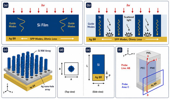
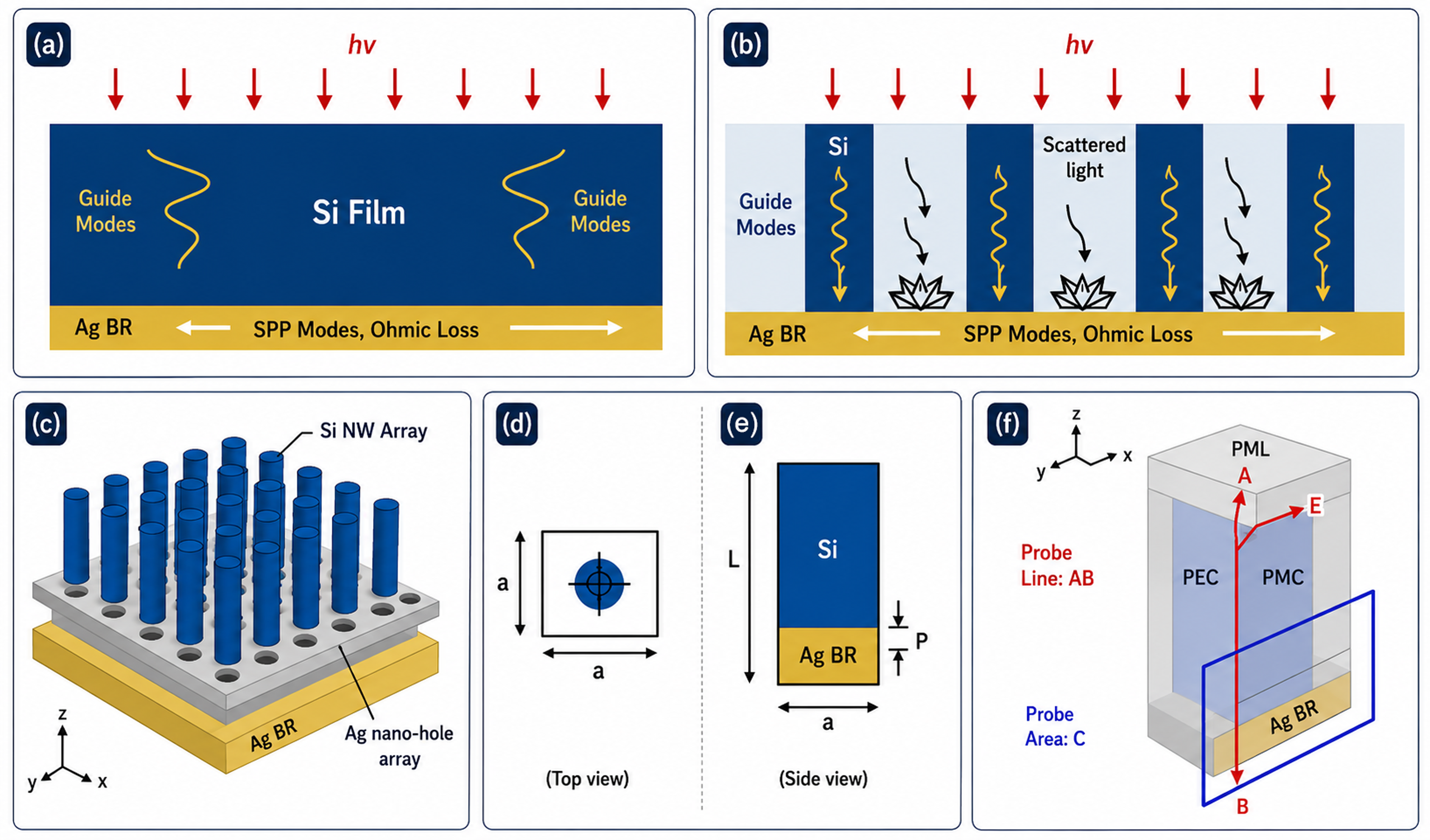
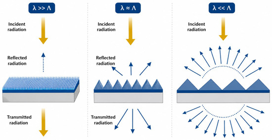
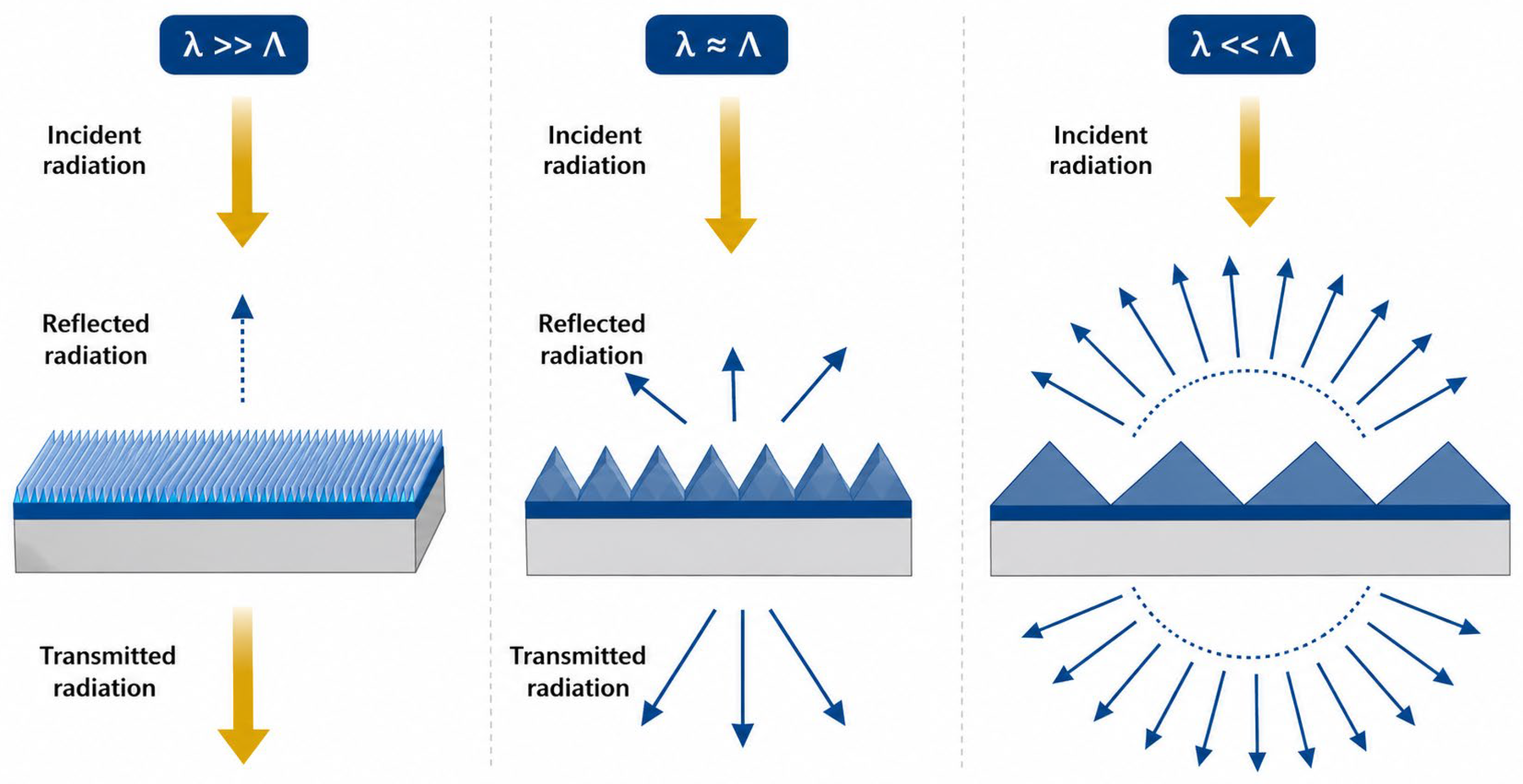
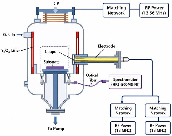
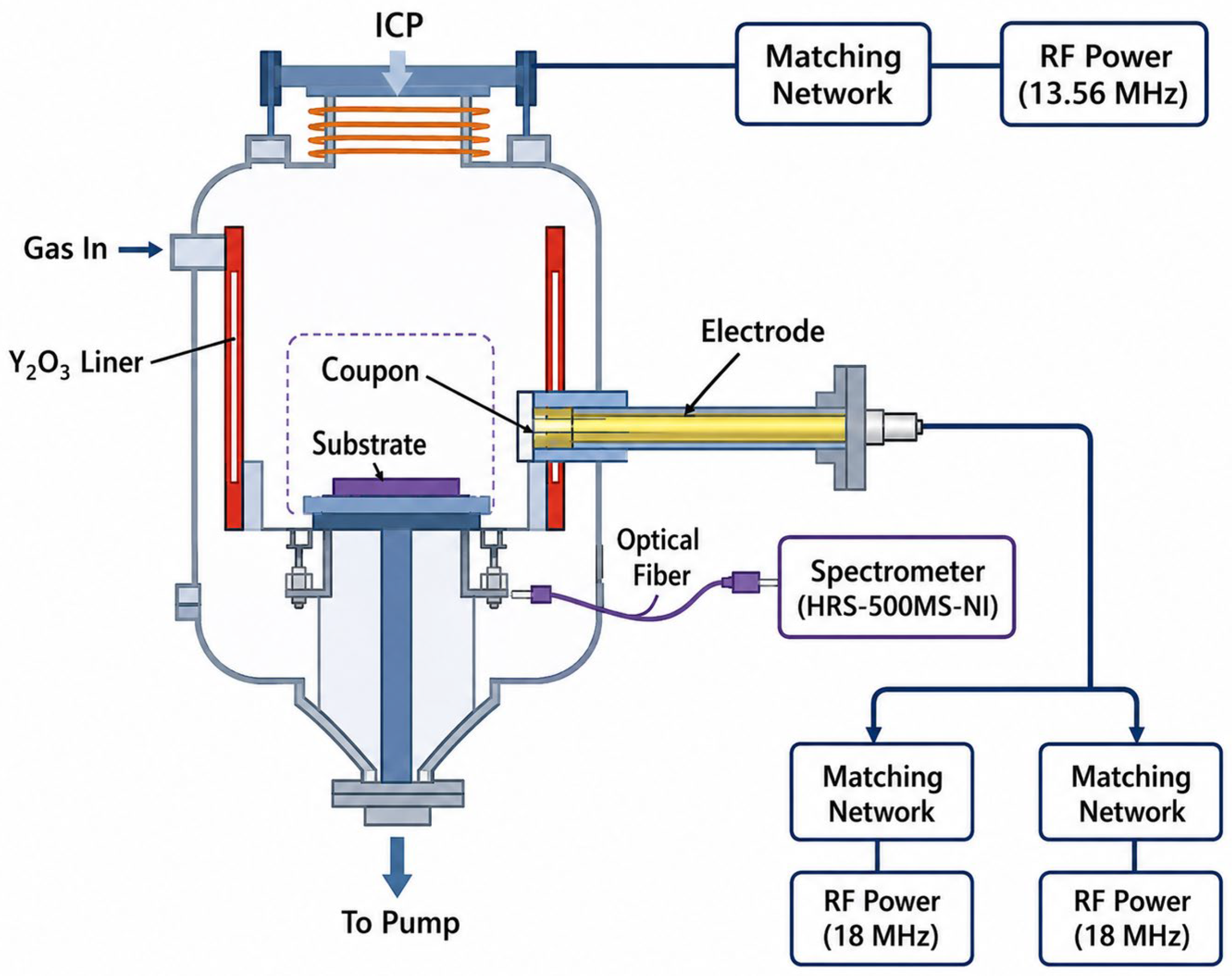
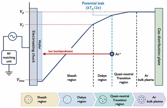
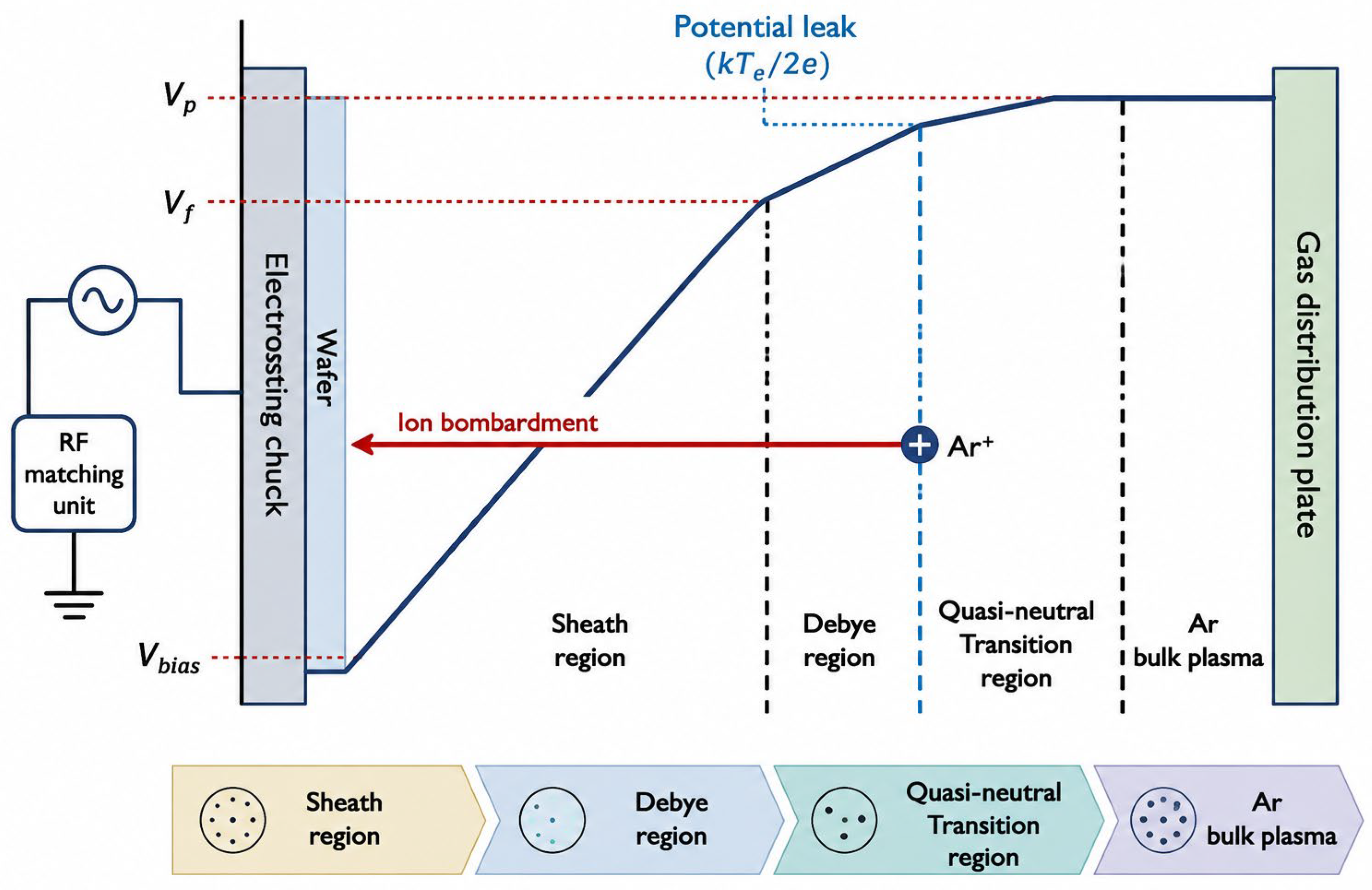
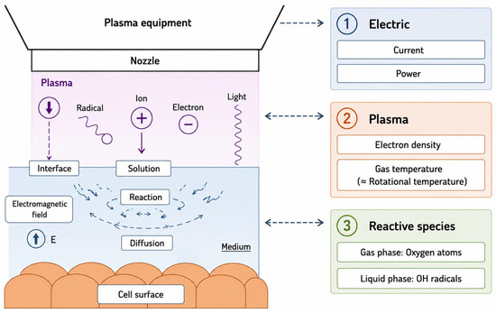
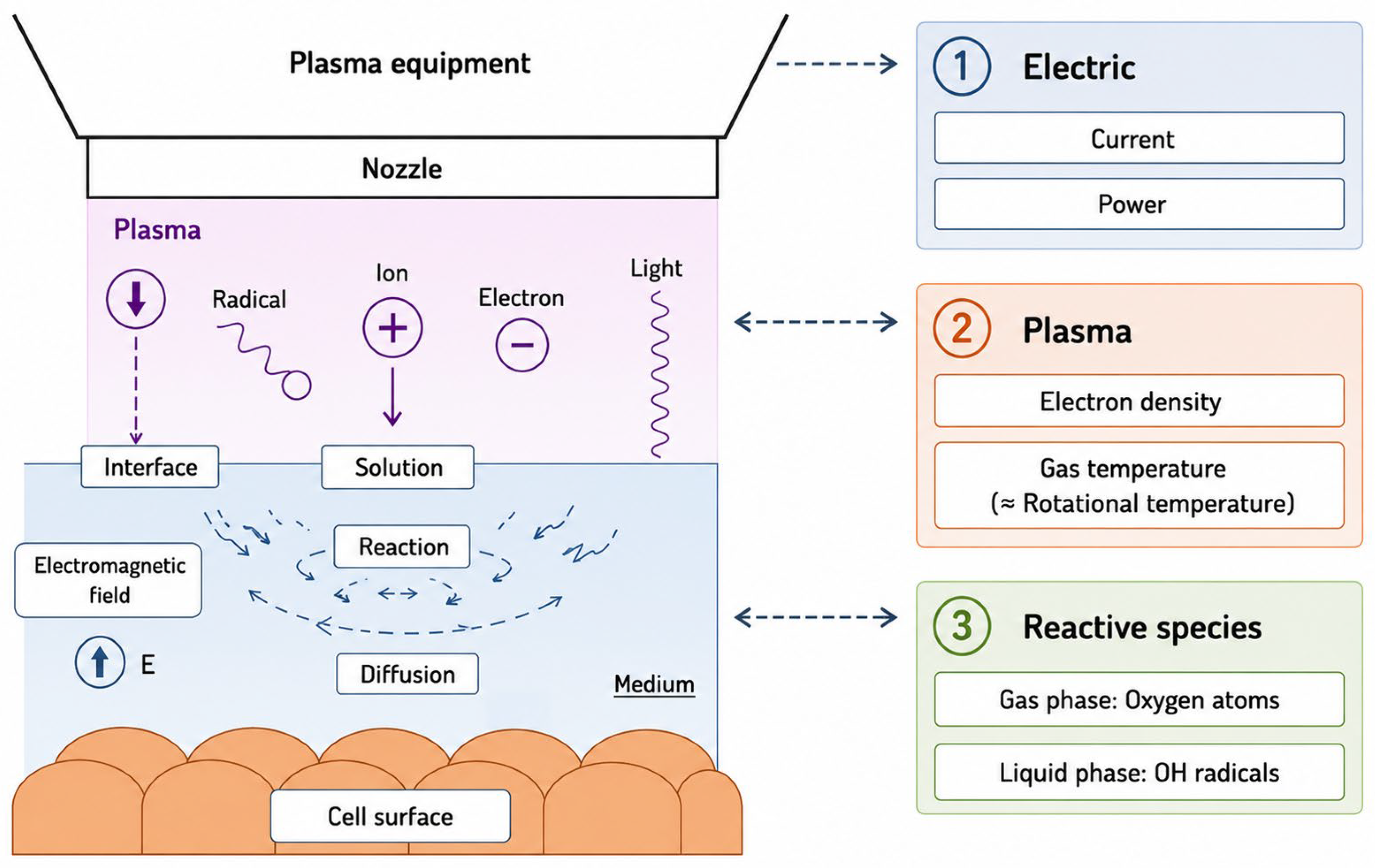
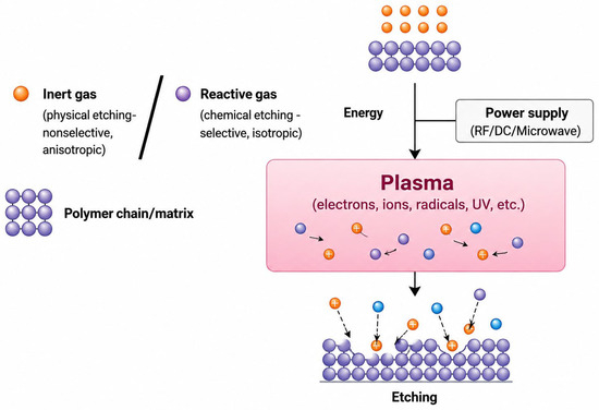
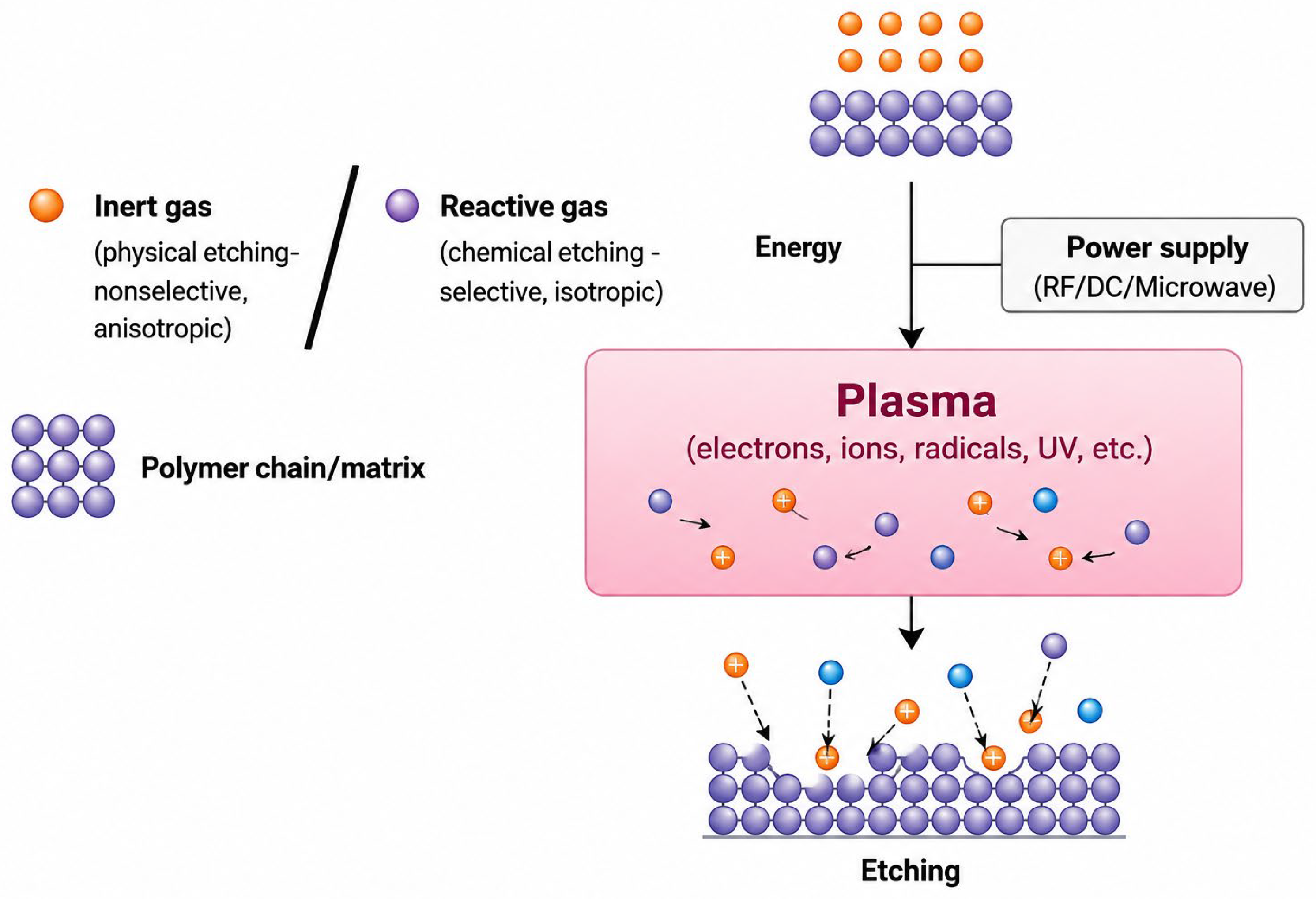
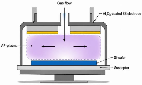
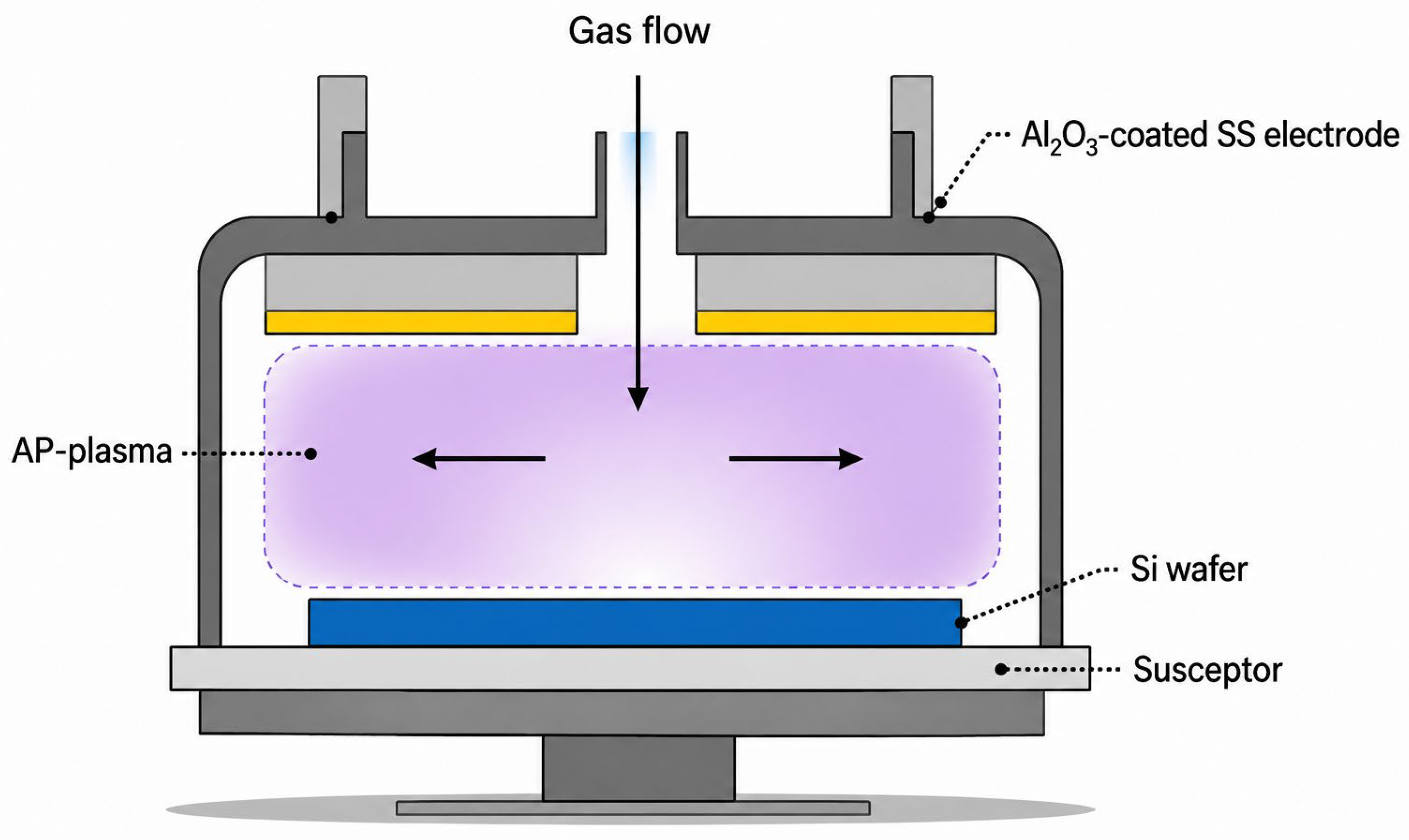
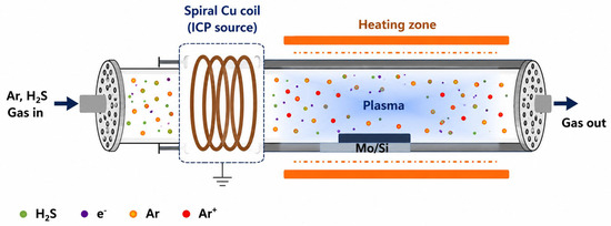
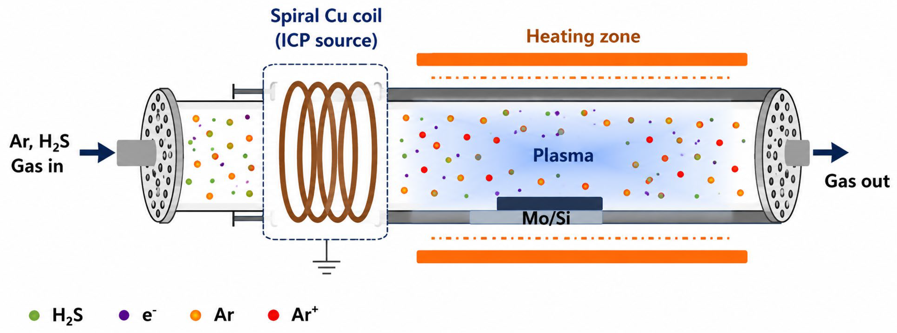
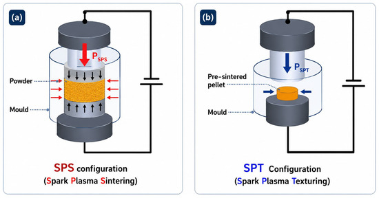
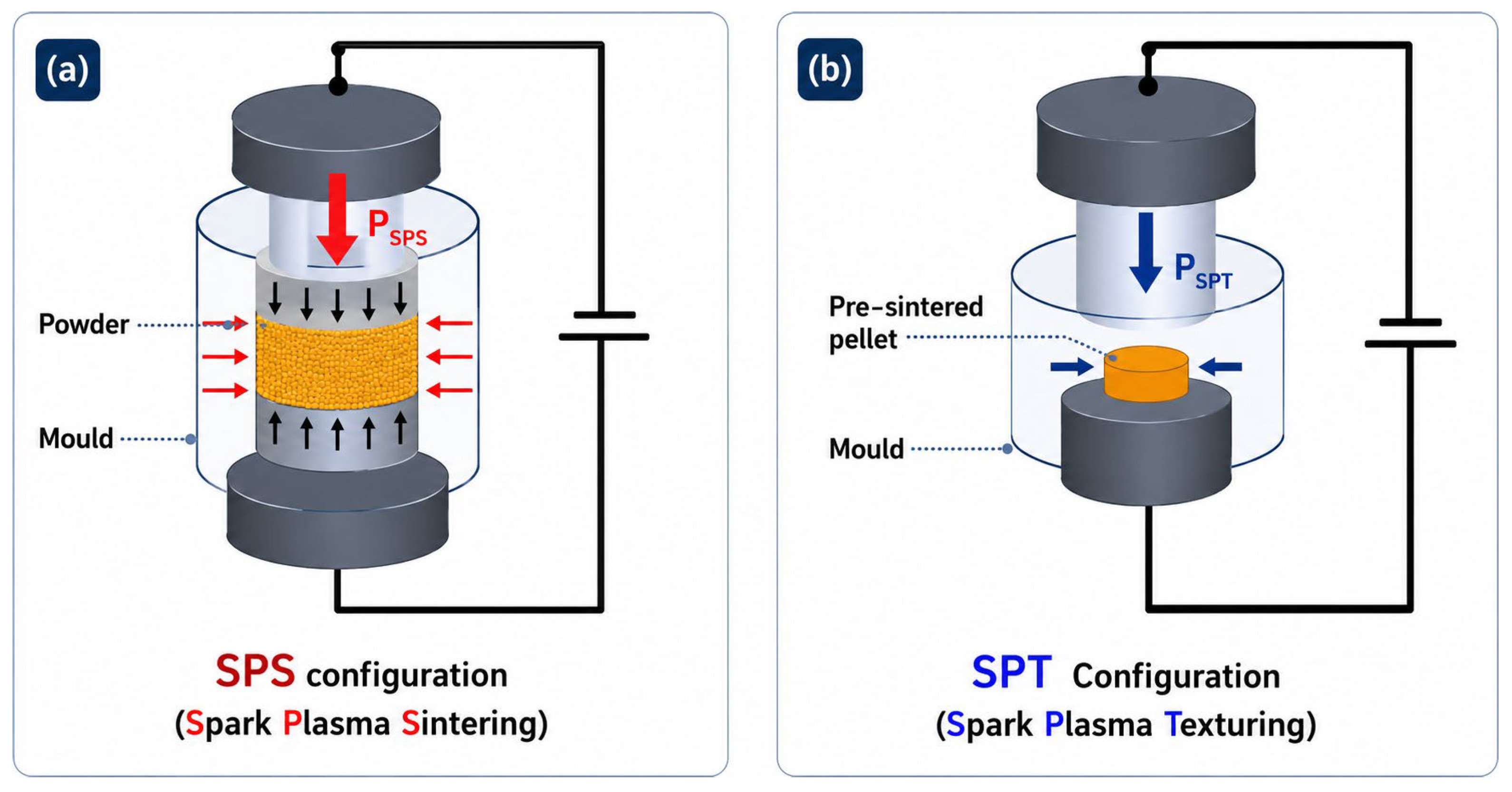

Disclaimer/Publisher’s Note: The statements, opinions and data contained in all publications are solely those of the individual author(s) and contributor(s) and not of MDPI and/or the editor(s). MDPI and/or the editor(s) disclaim responsibility for any injury to people or property resulting from any ideas, methods, instructions or products referred to in the content. |
© 2026 by the authors. Licensee MDPI, Basel, Switzerland. This article is an open access article distributed under the terms and conditions of the Creative Commons Attribution (CC BY) license.