


Abstract
Quantum dot light emitting diodes (QLEDs) have attracted considerable attention as next-generation display devices because of their high color purity, wide color gamut, and high luminous efficiency. Their performance is governed not only by the quantum dot emissive layer but also by the electron transport layer (ETL), which controls electron injection and transport, hole blocking, and interfacial recombination. In particular, metal oxide nanoparticles are widely used as ETL materials because of their high electron mobility, favorable energy level alignment with quantum dots, and compatibility with low temperature solution processing. QLEDs with ETLs based on metal oxide nanoparticles, however, suffer from excessive electron injection and surface defects such as oxygen vacancies and hydroxyl groups, which allow charge to accumulate at the interface and quench excitons, causing efficiency roll-off and limiting operational stability. Here, we review strategies developed to address these limitations, categorized into materials engineering (doping and surface treatment) and device structure engineering (interlayer insertion and double-layer ETLs).
1. Introduction
Growing demand for high resolution and high efficiency displays has intensified research on advanced optoelectronic materials, interface engineering, and device integration [1,2]. In particular, quantum dot light emitting diodes (QLEDs) have emerged as the most promising candidate in the display sector because of their high color purity, wide color gamut, high luminous efficiency, and high luminance [3,4], and they are widely regarded as a potential successor to organic light emitting diodes [5,6].
QLED performance is governed not only by the optical properties of the quantum dots (QDs) but also by the electrical and interfacial properties of the charge transport layers [7,8,9]. The electron transport layer (ETL) is particularly important because it controls electron injection and transport, hole blocking, charge balance, and interfacial nonradiative recombination, and therefore determines both the efficiency and operational stability of the device [10,11,12].
The development of QLEDs has been closely linked to advances in electron transport materials [13,14,15]. Early devices employed simple stacked structures such as indium tin oxide (ITO)/poly(p-phenylene vinylene)/CdSe QD/Mg, in which the recombination zone was poorly confined and charge injection and energy transfer proceeded through coupled pathways [16]. Consequently, parasitic emission contributed substantially to the electroluminescence spectrum [17].
QD emissive layers were subsequently sandwiched between organic hole transport layers (HTLs) and ETLs, while core/shell QDs were developed to passivate surface defects and improve exciton confinement [18,19,20]. These advances improved emission selectivity and photoluminescence, but the organic ETLs still suffered from low electron mobility, limited injection capability, and poor thermal and chemical stability [20,21,22]. Charge imbalance, high driving voltages, and external quantum efficiencies (EQEs) generally below 1% therefore remained the principal limitations [5,16,23].
The breakthrough came with metal oxide ETLs [24,25,26]. Among them, ZnO nanoparticles (NPs) became the representative ETL material, providing high electron mobility and favorable energy level alignment with QDs, low temperature solution processability, hole blocking capability, and thermal and chemical stability [27,28,29]. Their adoption substantially improved electron injection and transport and enabled the organic–inorganic hybrid device architectures in use today [24,30,31].
However, the high electron mobility and conductivity of ZnO can lead to excessive electron injection relative to hole injection, causing charge imbalance and interfacial charge accumulation in the QD emissive layer [9,32,33].
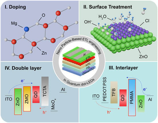
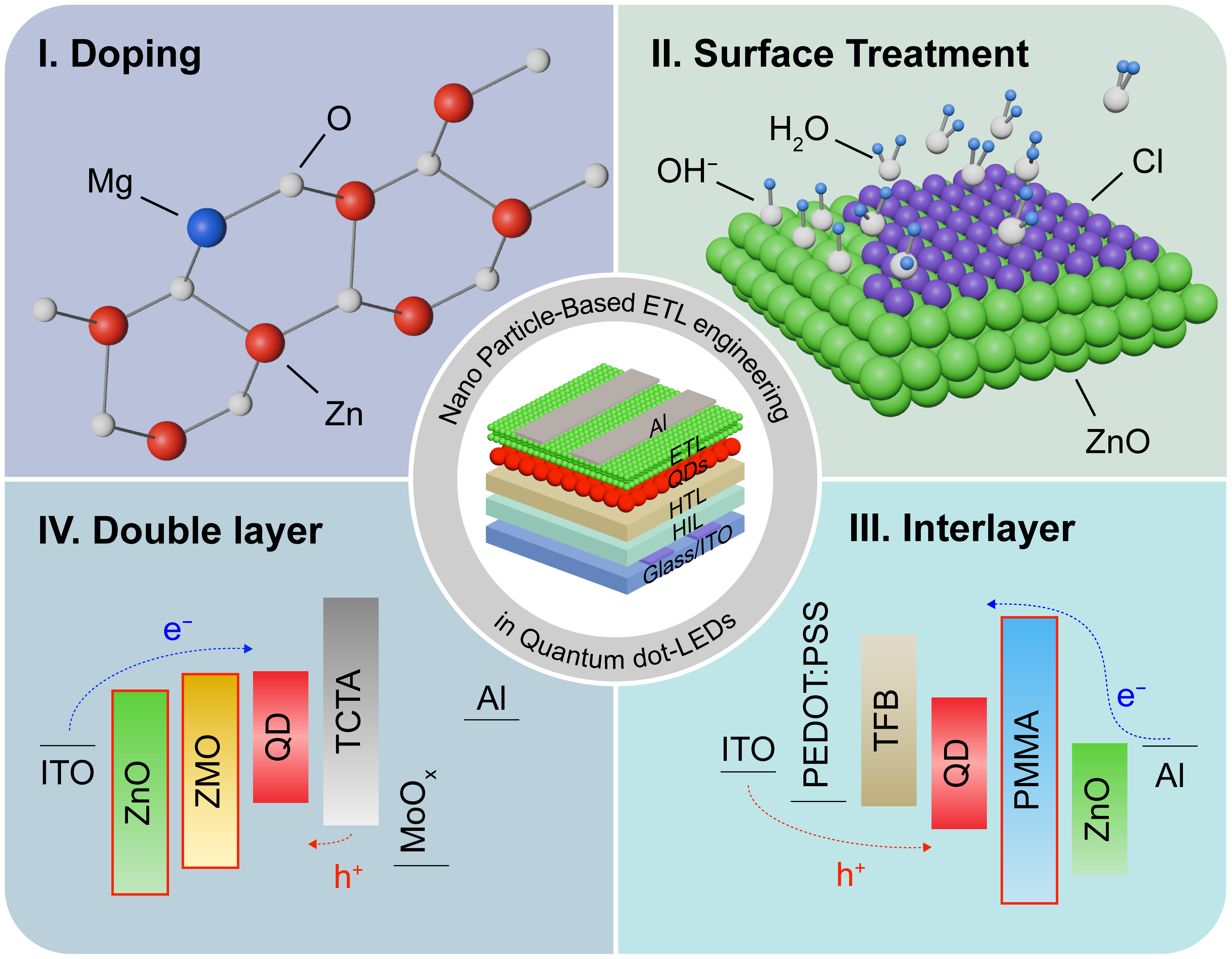
Here, we review the properties and limitations of ETLs based on metal oxide nanoparticles for QLEDs, together with the strategies developed to overcome them, organized into materials engineering and device structure engineering (Figure 1) [34]. We first discuss how the electrical and chemical properties of ETL materials are controlled by doping and surface treatment. We then compare interlayer and double layer strategies for controlling charge injection and stabilizing the QD/ETL interface, and assess their effects on efficiency, efficiency roll-off, and operational stability. Finally, we propose design directions and research priorities for ETLs based on metal oxide nanoparticles that achieve high efficiency and long lifetime simultaneously.
Figure 1.
ETL engineering strategies based on metal oxide nanoparticles for QLEDs: (I) doping, (II) surface treatment, (III) interlayer insertion, and (IV) double-layer ETL design.
2. Doping of ETLs with Metal Oxide Nanoparticles
Doping is one of the most effective routes to tune the electronic structure of the ETLs and, with it, device performance. ZnO, the most extensively studied and most widely used nanoparticle ETL material, is particularly amenable to such tuning through the incorporation of heteroatoms. Substituting dopants into the ZnO lattice shifts the conduction band minimum (CBM) and the Fermi level and also changes the carrier concentration, electrical conductivity, electron mobility, and defect state distribution. These changes provide direct control over the electron injection barrier and the charge transfer rate at the QD/ETL interface, and hence over the balance between electron and hole injection.
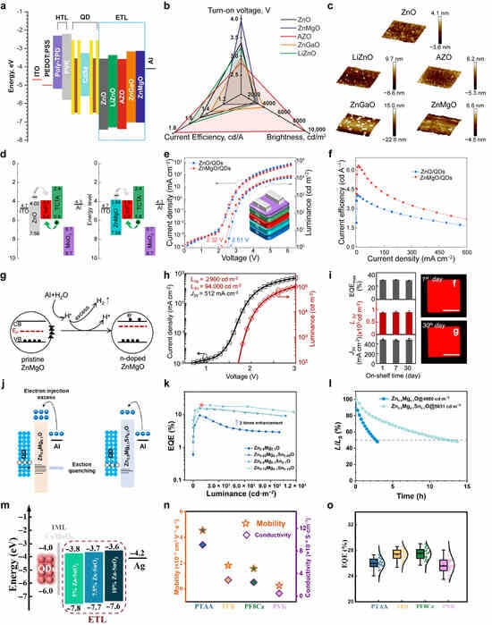
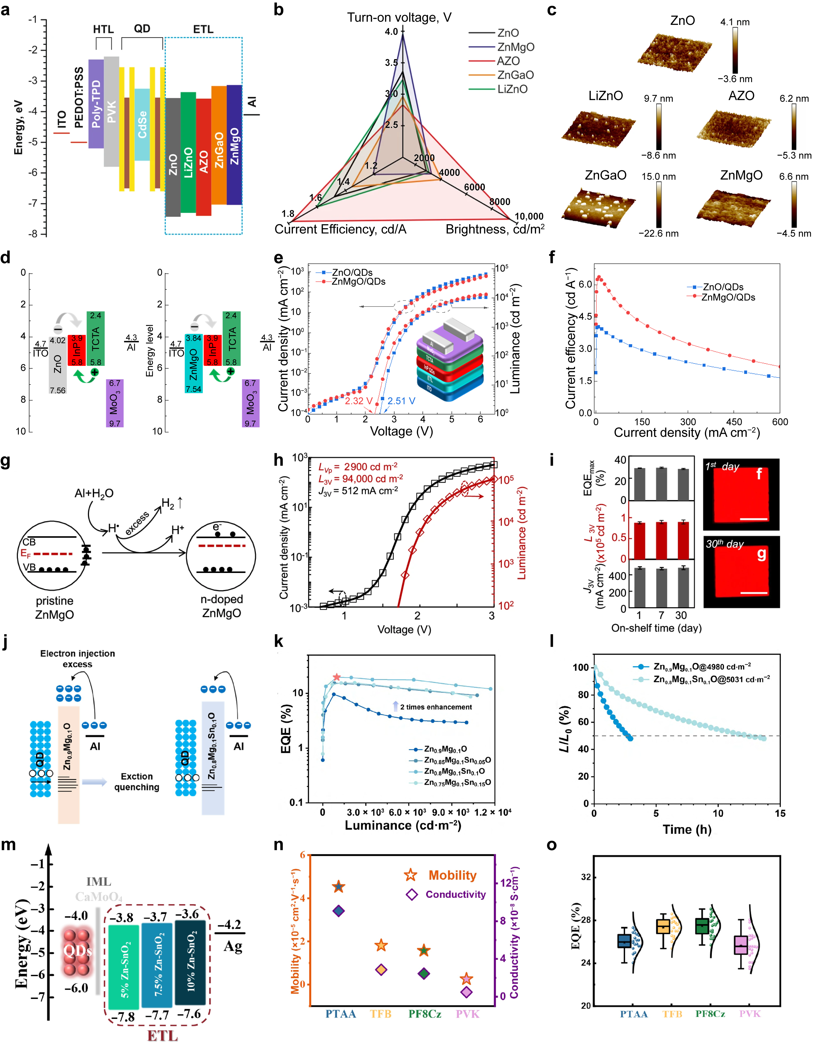
Alexandrov et al. compared ZnO NPs doped with Al, Ga, Mg, or Li as ETLs, evaluating both their electronic structure and the resulting QLED performance [35]. Dopant concentrations were set to 5% Mg, 10% Al, 5% Li, and 8% Ga, following compositions optimized in previous studies. Doping shifted the CBM and valence band maximum (VBM) of ZnO but left the bandgap essentially unchanged: 3.87, 3.93, 3.82, 3.86, and 3.90 eV for ZnO, LiZnO, aluminum-doped ZnO (AZO), ZnGaO, and ZnMgO (ZMO), respectively. For the comparison, conventional QLEDs were fabricated with the structure ITO/poly(3,4-ethylenedioxythiophene):poly(styrene sulfonate) (PEDOT:PSS)/poly[N,N′-bis(4-butylphenyl)-N,N′-bis(phenyl)benzidine] (poly-TPD)/poly(9-vinylcarbazole) (PVK)/QDs/(Li,Mg,Al,Ga)ZnO NPs/Al (Figure 2a), using QDs with a CdSe/ZnS/CdS/ZnS core/multishell structure. These QDs formed a very high electron injection barrier with the ETLs; although this degraded the overall device efficiency, it made the differences stand out in electron injection behavior between dopants. The AZO-based QLED exhibited the best performance, reaching a maximum luminance of 12,400 cd m−2, a current efficiency of 2.37 cd A−1, and a turn-on voltage of 2.8 V (Figure 2b). ZnGaO and ZMO formed more favorable CBM alignment with the QDs, but their relatively shallow VBMs reduced hole blocking capability and could permit leakage current, so the benefit of improved electron injection was partly offset by hole leakage. Atomic force microscopy images (Figure 2c) showed that AZO had a low and uniform surface roughness well suited to contact with both the QD layer and the Al electrode, whereas the ZnGaO film contained agglomerates larger than 30 nm despite a low average root-mean-square roughness, which would impede uniform charge transport. This study shows that QLED performance is not determined by CBM alignment alone: hole blocking by the VBM, electrical conductivity, and film morphology must be considered together. AZO performed best in these devices, but the optimum dopant would vary with QD composition, shell structure, and device architecture.
Figure 2.
Doping strategies for ETLs based on metal oxide nanoparticles in QLEDs. (a) Energy-level diagram of QLEDs employing ZnO, LiZnO, AZO, ZnGaO, and ZMO ETLs. (b) Comparison of turn-on voltage, maximum luminance, and current efficiency. (c) AFM images of the corresponding ETL films. (d) Energy-level alignment of ZnO- and ZMO-based QLEDs. (e) J-V-L characteristics. (f) Current efficiency as a function of current density. (g) Schematic of in situ reductive n-doping of ZMO. (h) J-V-L characteristics of the n-doped ZMO QLED. (i) Shelf stability of EQE, current density, and electroluminescence uniformity. (j) Schematic of electron injection and exciton quenching in pristine and ZMSO ETLs. (k) EQE as a function of luminance for QLEDs employing different Sn-doped ZnMgO ETLs. The red asterisk indicates the maximum EQE. (l) Operational lifetime comparison of pristine and ZMSO. (m) Energy-level diagram of QLEDs employing Zn-doped SnO2 ETLs with different doping concentrations. (n) Hole mobility and conductivity of PTAA, TFB, PF8Cz, and PVK. (o) EQE distributions of QLEDs employing different HTL materials. The individual data points represent the distribution of maximum EQE values. Adapted from: (a–c) Alexandrov et al. [35] (© The Authors 2020, CC BY 4.0); (d–f) Zhang et al. [36] (© The Authors 2021, CC BY 4.0); (g–i) Zheng et al. [37] (© The Authors 2025, CC BY 4.0); (j–l) Da et al. [38] (© The Authors 2026, CC BY 4.0); (m–o) Liu et al. [39] (© The Authors 2026, CC BY 4.0).
Doped ZnO is not limited to Cd-based QDs. It can also control electron injection barriers and interfacial defects in InP QD devices and in inverted architectures. Zhang et al. incorporated ZMO NPs containing approximately 12.2 mol% Mg into inverted red QLEDs with the structure ITO/ETL/InP QDs/4,4′,4″-tris(carbazol-9-yl)triphenylamine (TCTA)/MoO3/Al [36]. Mg doping left the VBMs unchanged, at 7.56 eV for ZnO and 7.54 eV for ZMO, but shifted the CBM from 4.02 to 3.84 eV (Figure 2d), so that the electron injection energy difference between the ETL and InP QDs changed from 0.12 to −0.06 eV. This change in energy level alignment decrease the turn-on voltage from 2.51 V for the ZnO device to 2.32 V for the ZMO device (Figure 2e), enhanced the maximum luminance from 1.0 × 10⁴ to more than 1.3 × 10⁴ cd m−2, and increased the maximum current efficiency from 4.03 to 6.38 cd A−1 (Figure 2f). This improvement was attributed not only to CBM tuning by Mg doping but also to a trap site reduction and interfacial nonradiative recombination decrease in the ZMO film. Mg doping is therefore an effective route to tailoring the electronic structure of ZnO to a given QD composition and device architecture.
Nanocrystalline ZnO and ZMO have conventionally been treated as n-type semiconductors, by analogy with their bulk counterparts. Zheng et al. showed instead that pristine ZMO nanocrystal films are weakly n-type and behave as nearly intrinsic semiconductors [37]. The resulting low electron conductivity and weak hole blocking account not only for high driving voltages and low luminance in QLEDs but also for the erratic positive aging induced by acid containing encapsulation. To address this, the authors developed an in situ reductive n-doping method in which reducing hydrogen species, generated by the reaction of the Al electrode with water vapor, fill the quantum confined conduction band edge states of the ZMO nanocrystals with electrons (Figure 2g). The treatment increases the free electron concentration and the Fermi level of ZMO, converting electron transport from space charge limited behavior to ohmic transport, and improving electron injection and hole blocking simultaneously. In devices with the structure ITO/PEDOT:PSS/HTL/QD monolayer/ZMO/Al and acid free encapsulation, a red QLED containing the in situ n-doped ZMO electron injection layer achieved a luminance of 2900 cd m−2 and a peak EQE of 28.9% at 1.93 V (Figure 2h), and the luminance increased steeply to 94,000 cd m−2 at 3 V. Unlike conventional QLEDs with acid containing encapsulation, which age erratically, these devices retained nearly constant EQE, luminance, current density, and emission uniformity after shelf storage (Figure 2i). In situ reductive n-doping therefore improves electron transport in ZMO and, at the same time, removes the encapsulation dependent positive aging that would otherwise obscure device performance.
Da et al. developed Sn4+/Mg2+ co-doped ZnO (ZMSO) NPs to address the efficiency and stability limitations of ZMO caused by oxygen vacancies and high chemical reactivity [38]. Uniform ZMSO NPs were synthesized using a microfluidic reactor, and the Sn doping concentration was set to 0, 5, 10, and 15%, with the Mg concentration fixed at 10% to optimize the electrical properties. Sn4+ incorporation strengthened metal–oxygen bonding and reduced oxygen vacancies. It also shifted the CBM from −3.37 to −3.19 eV and suppressed excessive electron injection (Figure 2j). These changes reduced interfacial charge accumulation and exciton quenching at the QD/ETL interface, improving the balance between electron and hole injection. To evaluate these effects, blue QLEDs were fabricated with the structure ITO/PEDOT:PSS/TFB/ZnSeTe QDs/ZMSO/Al. As shown in Figure 2k, the ZMSO-based QLED with 10% Sn doping achieved a maximum EQE of 19.7%, approximately twice that of the 9.6% obtained with the conventional ZMO ETL. Furthermore, the efficiency roll-off at 10,000 cd m−2 decreased from 69.3% to 31.2%. These improvements were attributed to the regulation of electron injection and the reduction of surface defects through Sn doping. Operational stability was also substantially enhanced. At an initial luminance of approximately 5000 cd m−2, the T50 (the time required for the luminance to decrease to 50% of its initial value, denoted LT50 in some of the reproduced figures) increased from 2.74 h for the ZMO device to 12.41 h for the ZMSO device (Figure 2l). When extrapolated to an initial luminance of 100 cd m−2, the T50 increased from 3931 to 18,236 h, representing an approximately 4.6-fold improvement. These lifetimes were extrapolated using a luminance-acceleration exponent of 1.86. The QLEDs were encapsulated with UV-curable resin, and the authors reported performing tests under ambient conditions. The electrical driving mode and quantitative encapsulation barrier performance were not specified.
Beyond ZnO-based ETLs, doping strategies have also been applied to SnO2 NPs to regulate electron transport and improve charge balance [39]. Liu et al. investigated Zn2+ doping of SnO2 NPs to address charge imbalance caused by their high electron mobility. Zn2+ doping concentrations were set to 5, 7.5, and 10% to control electron mobility and electrical conductivity. QLEDs were fabricated with the structure ITO/PEDOT:PSS/HTL/QDs/CaMoO4/Zn-SnO2/Ag. Increasing the Zn2+ content from 5 to 10% shifted the CBM of SnO2 upward from −3.8 to −3.6eV, increasing the electron injection barrier (Figure 2m), while reducing electron mobility and electrical conductivity to suppress excessive electron injection. These changes allowed the electron transport properties of SnO2 to be matched with the different hole transport characteristics of various HTLs. The four HTL investigated were poly[bis(4-phenyl)(2,4,6-trimethylphenyl)amine] (PTAA), poly[(9,9-dioctylfluorenyl-2,7-diyl)-co-(4,4′-(N-(4-sec-butylphenyl))diphenylamine)] (TFB), poly[(9,9-dioctylfluorenyl-2,7-diyl)-alt-(9-(2-ethylhexyl)carbazole-3,6-diyl)] (PF8Cz), and PVK. As shown in Figure 2n, PTAA exhibited the highest hole mobility and electrical conductivity, whereas PVK showed the lowest values. TFB and PF8Cz exhibited intermediate transport properties. Accordingly, the Zn doping concentration was optimized for each HTL to improve the balance between electron and hole injection. The highest device efficiencies were obtained at Zn doping concentrations of 5% for PTAA, 7.5% for TFB and PF8Cz, and 10% for PVK. Figure 2o shows the distributions of peak EQE measured from 20 QLEDs for each HTL, with average peak EQEs of 26.0, 27.3, 27.5, and 25.7% for PTAA-, TFB-, PF8Cz-, and PVK-based devices, respectively. In particular, the PF8Cz-based QLED achieved a maximum EQE of 29.1%, while the optimized devices with all four HTLs exhibited maximum EQEs exceeding 27%. This study demonstrates that precise control of electron transport properties through Zn doping enables SnO2 ETLs to accommodate various HTLs, improving charge balance and luminous efficiency.
3. Surface Treatment of ETLs with Metal Oxide Nanoparticles
Advances in ETL materials and doping strategies have substantially improved charge injection and transport in QLEDs. Stoichiometric and structural defects in metal oxide NPs nevertheless remain a limiting factor, as do the surface defects that follow from their high surface-to-volume ratio. These defects act as charge trapping sites and nonradiative recombination centers within the ETL and at the QD/ETL interface, impeding charge transport and causing charge imbalance and exciton quenching, and weakening long-term operational stability. Highly efficient and stable QLEDs therefore require passivation strategies that suppress surface defects and interfacial reactivity, in addition to control of the ETL electronic structure.
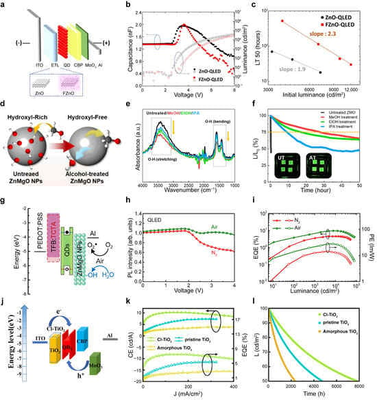
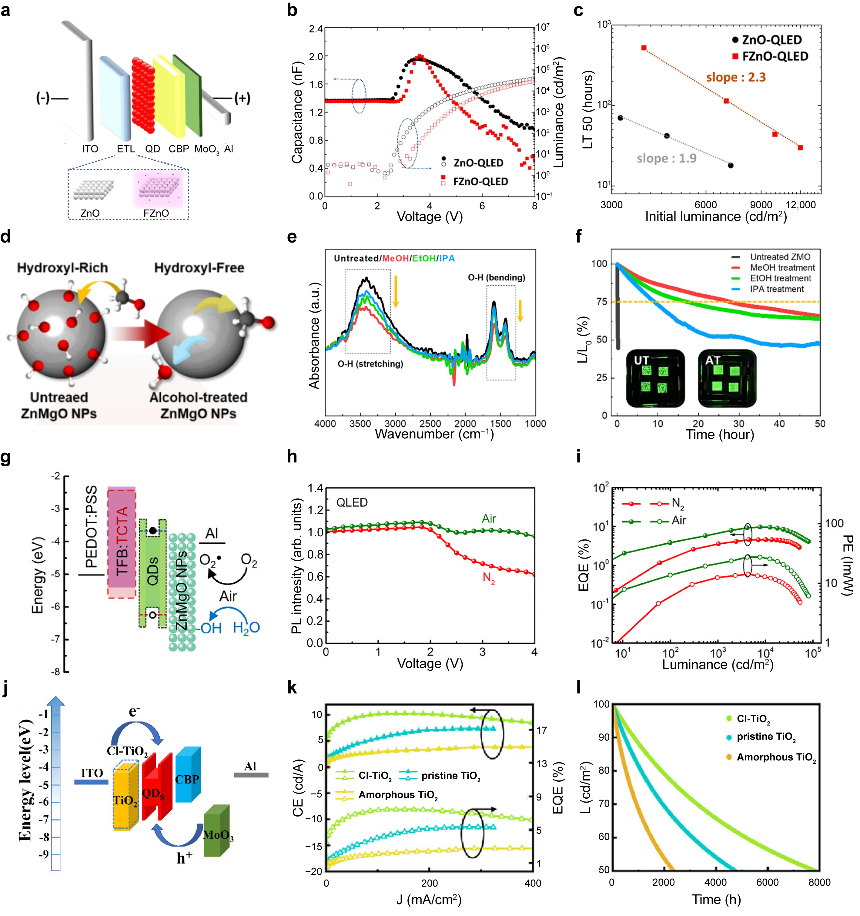
Chung et al. passivated the ZnO NP ETL in QLEDs by fluorine plasma treatment using carbon tetrafluoride (CF4) as the source gas [40]. Fluorine atoms are considered to passivate oxygen vacancies in the ZnO lattice and to bond to undercoordinated Zn2+ sites, which reduces oxygen vacancy-related trap states. Inverted red QLEDs with the structure ITO/ETL/QD/4,4′-bis(N-carbazolyl)-1,1′-biphenyl (CBP)/MoO3/Al were fabricated with either untreated ZnO or CF4-plasma treated ZnO (FZnO), denoted ZnO-QLED and FZnO-QLED, respectively (Figure 3a). Both devices reached similar peak capacitances at approximately 3.8 V in capacitance–voltage–luminance measurements, but above this voltage, the capacitance of the FZnO-QLED decreased more rapidly (Figure 3b), indicating faster annihilation of the charge accumulated at the QD/CBP interface by electron hole recombination. In Cd-based QLEDs, the large hole injection barrier between the QDs and the HTL allows holes to accumulate at the QD/HTL interface, accelerating interfacial degradation and shortening device lifetime. The FZnO ETL appears to increase the effective electron concentration in the QDs and at the QD/HTL interface, relieving this hole accumulation. As shown in Figure 3c, the extrapolated T50 at an initial luminance of 100 cd m−2 was 2.37 × 10⁶ h for the FZnO-QLED, representing a 47-fold increase compared with approximately 5.0 × 10⁴ h for the ZnO-QLED. Fluorine passivation therefore improves long-term stability by reducing defects in ZnO while redistributing charge at the QD/HTL interface. The directly measured T50 values were 65 h for the ZnO-QLED and 516 h for the FZnO-QLED under a constant current density of 20 mA cm−2, with initial luminances of 3320 and 3910 cd m−2, respectively. The reported lifetimes at 100 cd m−2 were extrapolated using acceleration exponents of 1.9 and 2.3, respectively. The encapsulation procedure and lifetime-test atmosphere were not specified.
Figure 3.
Surface-treatment strategies for ETLs based on metal oxide nanoparticles in QLEDs. (a) Device structure employing ZnO or fluorine-passivated ZnO ETLs. (b) Capacitance–voltage–luminance characteristics. (c) T50 as a function of initial luminance (LT50 is equivalent to T50 as used in the text). (d) Schematic of hydroxyl removal from ZMO NPs by alcohol treatment. (e) FT-IR spectra of untreated and alcohol-treated ZMO films. (f) Operational luminance decay of the corresponding QLEDs. (g) Energy-level diagram and humid-air treatment of the ZMO ETL. (h) Voltage-dependent PL intensity under N2 and air exposure. (i) EQE and power efficiency as functions of luminance. (j) Energy-level diagram of the Cl- TiO2 QLED. (k) Current efficiency and EQE versus current density. (l) Operational lifetime characteristics of Cl-TiO2, pristine TiO2, and amorphous TiO2 devices. Adapted from: (a–c) Chung et al. [40] (© Crown 2022, CC BY 4.0); (d–f) Oh et al. [41] (© The Authors 2025, CC BY 4.0); (g–i) Chrzanowski et al. [42] (© The Authors 2021, CC BY 4.0); (j–l) Liu et al. [43] (© The Authors 2025, CC BY 4.0).
Mg incorporation into ZnO tunes energy level alignment and certain defect states, but the high surface-to-volume ratio of ZMO NPs results in residual surface hydroxyl groups (-OH) that form charge trapping sites and surface dipoles, impeding charge transport and degrading efficiency and operational stability. To address this issue, Oh et al. prepared hydroxyl free ZMO NP thin films using an alcohol treatment [41]. Methanol (MeOH), ethanol (EtOH), and isopropanol (IPA) remove surface -OH species through hydrogen bonding and proton transfer, which reduces charge traps and dipole moments (Figure 3d). Fourier transform infrared (FT-IR) spectra of ZMO NP films showed weaker -OH absorption for alcohol treatment than for untreated ZMO (Figure 3e), with the largest reduction for MeOH, followed by EtOH and IPA. This trend was attributed to the higher polarity and smaller molecular size of MeOH, which give it faster and more effective access to the NP surface. The passivation is directly related to operational stability. At an initial luminance of 500 cd m−2, the untreated QLED reached the time to 75% of the initial luminance (T75) within approximately 4 min, whereas the MeOH, EtOH, and IPA treated QLEDs exhibited T75 values of approximately 28, 17, and 9 h, respectively (Figure 3f). The T75 measurements were reported under ambient conditions, whereas the electrical driving mode and any encapsulation procedure were not explicitly specified. The results are associated with the extent of -OH removal observed by FT-IR. A simple alcohol treatment can suppress electron trapping and surface dipoles, and markedly improve charge transport and operational stability, without changing the ZMO composition or device architecture.
Air exposure is generally considered detrimental to devices, but Chrzanowski et al. showed that controlled humid air exposure can be beneficial. It terminates some active sites on the ZMO NP surface with -OH and promotes O2 adsorption, which changes charge transport in the ETL [42]. Devices with the structure ITO/PEDOT:PSS/poly[(9,9-dioctylfluorenyl-2,7-diyl)-co-(4,4′-(N-(4-sec-butylphenyl))diphenylamine)](TFB):TCTA/QDs/ZMO/Al were fabricated (Figure 3g), and devices processed entirely under N2 were compared with devices whose ZMO layer was exposed to humid air at approximately 50% relative humidity for 5–10 min before Al deposition. At about 3.3 V, where the maximum EQE was obtained, the air exposed device showed an approximately 40% higher voltage-dependent photoluminescence quantum yield (PLQY) than the N2-processed device (Figure 3h). Excessive electron charging of the QD layer and the Auger recombination that comes from it were suppressed under bias, allowing the QDs to remain in a more electrically neutral state. The air exposed device showed more than twofold improvements in both EQE and luminance compared with the device processed under N2, with an average EQE of 7.1%, a maximum EQE of 9.5%, and maximum power and current efficiencies of 30 lm W−1 and 30 cd A−1, respectively (Figure 3i). H2O and O2 adsorbed on the ZMO NP surface do not act merely as impurities. They suppress hole leakage and excessive electron injection simultaneously, improving charge balance in the QD layer.
Although TiO2 offers superior chemical stability compared with ZnO, conventional TiO2 ETLs often suffer from insufficient crystallinity, insulating surface ligands, and high electron injection barriers, resulting in lower device performance than ZnO-based QLEDs. In particular, the rapid hydrolysis and condensation of Ti precursors can lead to amorphous structures, while long-chain insulating ligands used to stabilize TiO2 nanoparticles can restrict electron transport. Liu et al. replaced ZnO with a surfactant-free and highly dispersed crystalline anatase TiO2 NP ETL modified with chlorine (Cl-TiO2) in order to achieve superior atmospheric stability [43]. Chlorine modification passivates catalytically active sites on the TiO2 NP surface and reduces surface adsorbed hydroxyl clusters and H2O that act as exciton quenching sites. This suppresses nonradiative recombination at the Cl-TiO2/QD interface and also tunes the surface potential and energy levels of Cl-TiO2, lowering the electron injection barrier by approximately 0.11 eV. Inverted red QLEDs were fabricated with the structure ITO/ETL/QDs/CBP/MoO3/Al (Figure 3j). The combination of high crystallinity, chlorine passivation, and a reduced injection barrier gave a peak current efficiency of 10.27 cd A−1 and a maximum EQE of 7.44% (Figure 3k), 39.5% and 39.6% higher, respectively, than the 7.36 cd A−1 and 5.33% of the pristine TiO2 device. Operational stability was evaluated on encapsulated devices at room temperature under dark conditions. The extrapolated T50 was 7838 h for the Cl-TiO2 device, 64.8% longer than the 4755 h of the pristine TiO2 device (Figure 3l) and approximately 3.3 times the 2363 h of the device with an air-processed ZnO ETL. The measured T50 was 6.86 h at an initial luminance of 5000 cd m−2. Although the devices were encapsulated and assessed at room temperature under dark conditions, the lifetime-test driving mode, testing atmosphere, encapsulation barrier performance, and parameters used for extrapolation were not explicitly reported. Combining the chemical stability of TiO2 with chlorine surface passivation improves ETL conductivity, electron injection, and TiO2/QD interfacial stability simultaneously. Because Cl-TiO2 is less sensitive than ZnO to H2O and O2 and retains its properties under ambient processing, it is a promising alternative nanoparticle ETL for QLEDs that require both high efficiency and long operational lifetime.
4. Interlayer Insertion
Charge imbalance in QLEDs arises for two reasons: the hole injection barrier into the QD layer is larger than the electron injection barrier, and the electron mobility of a ZnO-based ETL exceeds the hole mobility of an organic HTL. The resulting asymmetric injection and transport allow excess electrons to accumulate in the QD layer, leading to Auger recombination, exciton quenching, and efficiency roll-off. Inserting an interlayer between the ZnO ETL and the QD layer is a representative approach. An interlayer improves charge balance by limiting the electron flux from ZnO into the QDs, and suppresses interfacial charge transfer and exciton quenching by preventing direct contact between ZnO and the QDs. The material, thickness, concentration, and position of the interlayer are therefore all critical to efficiency and operational stability.
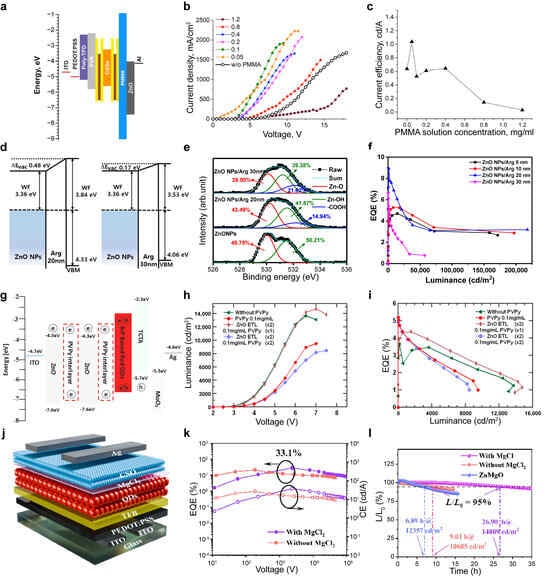
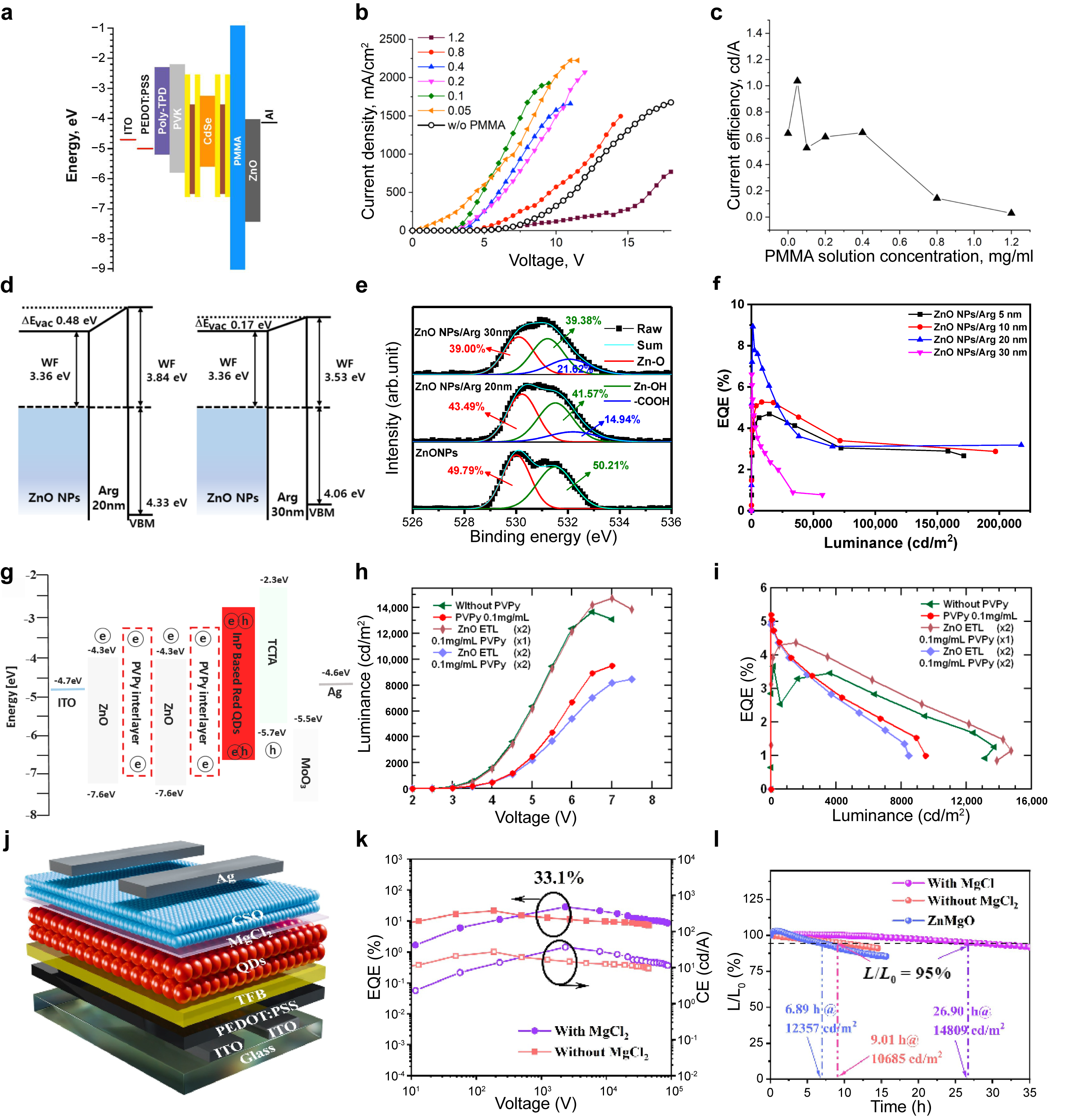
A thin poly(methyl methacrylate) (PMMA) film presents a potential barrier high enough to restrict electron injection from the ZnO ETL into the QD emissive layer, and it is widely used as an interlayer or electron blocking layer. Zvaigzne et al. optimized electron injection and charge balance by varying the concentration of the PMMA solution [44]. Devices with the structure ITO/PEDOT:PSS/poly-TPD/PVK/QD/PMMA/ZnO/Al were prepared at PMMA concentrations of 0.05, 0.1, 0.2, 0.4, 0.8, and 1.2 mg mL−1 (Figure 4a). PMMA containing devices generally exhibited higher current densities than the PMMA free control device (Figure 4b). Although PMMA forms a high potential barrier of approximately 3 eV, suppressing excess electron injection and interfacial charge accumulation improved the current flow. At 1.2 mg mL−1, however, the thicker PMMA layer overly suppressed electron tunneling and reduced both current density and luminance. At 0.05 mg mL−1, the device showed the highest nominal performance, with a low turn-on voltage of 2.1 V, a maximum current efficiency of 0.99 cd A−1, and a maximum luminance of 18,671 cd m−2, but it also showed leakage current between 0 and 2.5 V. The authors identified 0.4 mg mL−1 as the optimum condition, with a maximum current efficiency of 0.95 cd A−1 (Figure 4c). This value was marginally lower than at 0.05 mg mL−1, but its electron blocking was more stable once low voltage leakage was taken into account.
Figure 4.
Interlayer engineering strategies for QLEDs. (a) Energy-level diagram of the PMMA-interlayer device. (b) Current density–voltage characteristics at different PMMA concentrations. (c) Maximum current efficiency as a function of PMMA concentration. (d) Energy-level diagrams of ZnO/Arg interlayers with thicknesses of 20 and 30 nm. (e) O 1s XPS spectra of ZnO and Arg-modified ZnO films. (f) EQE–luminance characteristics for different Arg thicknesses. (g) Energy-level diagram of PVPy-containing device structures. (h) Luminance–voltage characteristics of the single- and double-PVPy configurations. (i) Corresponding EQE–luminance characteristics. (j) Schematic device structure of Co–SnO2-based QLEDs incorporating an MgCl2 interlayer. (k) EQE and current efficiency as functions of voltage for QLEDs with and without MgCl2. (l) Operational lifetimes of CSO-based QLEDs with and without MgCl2 and of a ZnMgO-based QLED. Adapted from: (a–c) Zvaigzne et al. [44] (© The Authors 2021, CC BY 4.0); (d–f) Chae et al. [45] (© The Authors 2024, CC BY 4.0); (g–i) Kiguye et al. [46] (© The Authors 2023, CC BY 4.0); (j–l) Wang et al. [47] (© The Authors 2026, CC BY 4.0).
Chae et al. inserted arginine (Arg) between ZnO NPs and the QD layer in order to regulate electron injection and the ZnO surface simultaneously [45]. Devices with the structure ITO/ZnO NPs/Arg/QD/TCTA/WOx/Ag were fabricated with Arg thicknesses of 5, 10, 20, and 30 nm. Ultraviolet photoelectron spectroscopy showed a work function of 3.36 eV for bare ZnO, increasing to 3.56, 3.67, and 3.84 eV at Arg thicknesses of 5, 10, and 20 nm, with vacuum level shifts of 0.20, 0.31, and 0.48 eV, respectively. At 30 nm, the work function and vacuum level shift decreased to 3.53 and 0.17 eV (Figure 4d), so the interfacial-dipole-induced electron injection barrier was largest at 20 nm. O 1s X-ray photoelectron spectra showed that, as the Arg thickness increased from 0 to 5, 10, 20, and 30 nm, the Zn-OH component decreased from 50.21% to 47.00%, 44.33%, 41.57%, and 39.38%, while the -COOH component increased from 0 to 5.52%, 10.86%, 14.94%, and 21.62%, respectively (Figure 4e). These results indicate that Arg removes hydroxyl groups from the ZnO surface and reduces interfacial quenching sites. By balancing electron injection against surface passivation, the device with a 20 nm Arg interlayer achieved a maximum EQE of 8.93% (Figure 4f). At 30 nm, performance declined despite the further loss of hydroxyl groups, because the thicker insulating Arg layer then restricted electron transport too strongly.
Kiguye et al. investigated how the position and number of layers of the insulating polymer poly(4-vinylpyridine) (PVPy) affect electron injection [46]. The device structure was ITO/ZnO/PVPy/InP-based red QDs/TCTA/MoO3/Ag. The authors compared three device configurations with a PVPy free reference device. These were a 0.1 mg mL−1 PVPy layer on a single ZnO ETL, a ZnO/PVPy/ZnO structure with PVPy sandwiched between two ZnO layers, and a ZnO/PVPy/ZnO/PVPy structure (Figure 4g). PVPy restricts excessive electron injection into the QD layer through its insulating character, but the degree of electron blocking depends on where it is located and how many layers are deposited. With 0.1 mg mL−1 PVPy on a single ZnO ETL, the maximum luminance decreased from 13,700 cd m−2 for the reference device to 9501 cd m−2, while the EQE at 100 cd m−2 increased from 2.96% to 4.06% (Figure 4h,i). PVPy in direct contact with the QD layer improved charge balance by suppressing electron injection, but limited electron transport at the same time. The ZnO/PVPy/ZnO structure retained electron injection through the second ZnO layer in contact with the QDs and exhibited the highest maximum luminance of 14,750 cd m−2, together with an EQE at 100 cd m−2 of 3.36%, above that of the reference device. The ZnO/PVPy/ZnO/PVPy structure blocked electrons more strongly because of the additional PVPy layer adjacent to the QDs. The device showed that the EQE at 100 cd m−2 increased to 4.11%, but the maximum luminance decreased to 8446 cd m−2. A PVPy interlayer can improve charge balance, but inserting it directly at the QD interface, or stacking multiple layers, restricts electron transport excessively. As a result, the ZnO/PVPy/ZnO structure offered the best trade-off between efficiency and luminance.
Although SnO2 offers superior environmental stability compared with ZnO, its electroluminescent performance can be limited by excessive surface hydroxyl groups and high electron mobility, which contribute to interfacial exciton quenching and charge imbalance, respectively. Wang et al. introduced an MgCl2 interlayer to suppress interfacial exciton quenching and improve charge balance in QLEDs employing Co-doped SnO2 (CSO) ETLs. Co doping reduced oxygen vacancies in SnO2 and increased the electron injection barrier, improving charge balance [47]. However, excessive electron injection at high luminance still caused significant efficiency roll-off. To address this limitation, QLEDs were fabricated with the structure ITO/PEDOT:PSS/TFB/QDs/MgCl2/CSO/Ag (Figure 4j), in which an approximately 7 nm thick MgCl2 interlayer was inserted between the QD layer and the CSO ETL. Cl− ions in MgCl2 passivated interfacial oxygen vacancies and surface defects, suppressing nonradiative recombination, while the interfacial dipole effect was proposed to improve charge balance by regulating energy level alignment and restricting excessive electron injection, thereby improving charge balance. As shown in Figure 4k, the maximum EQE increased from 21.5% for the QLED with a 5 wt.% CSO ETL to 33.1% upon MgCl2 insertion. This improvement was attributed to reduced exciton quenching through interfacial defect passivation and controlled electron injection. Operational stability was also substantially enhanced. The MgCl2-containing QLED exhibited a T95 lifetime of 26.90 h at an initial luminance of 14,809 cd m−2, and the extrapolated T95 at 1000 cd m−2 reached 3367.7 h, representing a 5.36-fold improvement over the device without MgCl2 (Figure 4l). Operational stability was measured under constant-current driving, and the T95 at 1000 cd m−2 was extrapolated from the measured high-luminance value using an acceleration exponent of 1.792. Although the devices were fabricated in a nitrogen-filled glovebox, the lifetime-test atmosphere, encapsulation procedure, and quantitative barrier performance were not specified. This study demonstrates that interlayer engineering combining interfacial defect passivation and charge injection regulation is an effective strategy for improving both the luminous efficiency and long-term operational stability of SnO2-based QLEDs.
5. Double-Layer ETL
In a single ETL, electron transport, energy level alignment, and interfacial stability all depend on one material, which creates a trade-off between high electron mobility and appropriately controlled electron injection. A double-layer ETL stacks two materials with complementary properties. One layer maintains efficient electron transport, while the other regulates electron injection, defects, and charge accumulation at the QD interface. Unlike an insulating interlayer, this architecture preserves the electron transport pathway while improving charge balance, luminance, and operational stability.
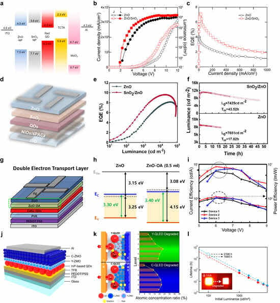
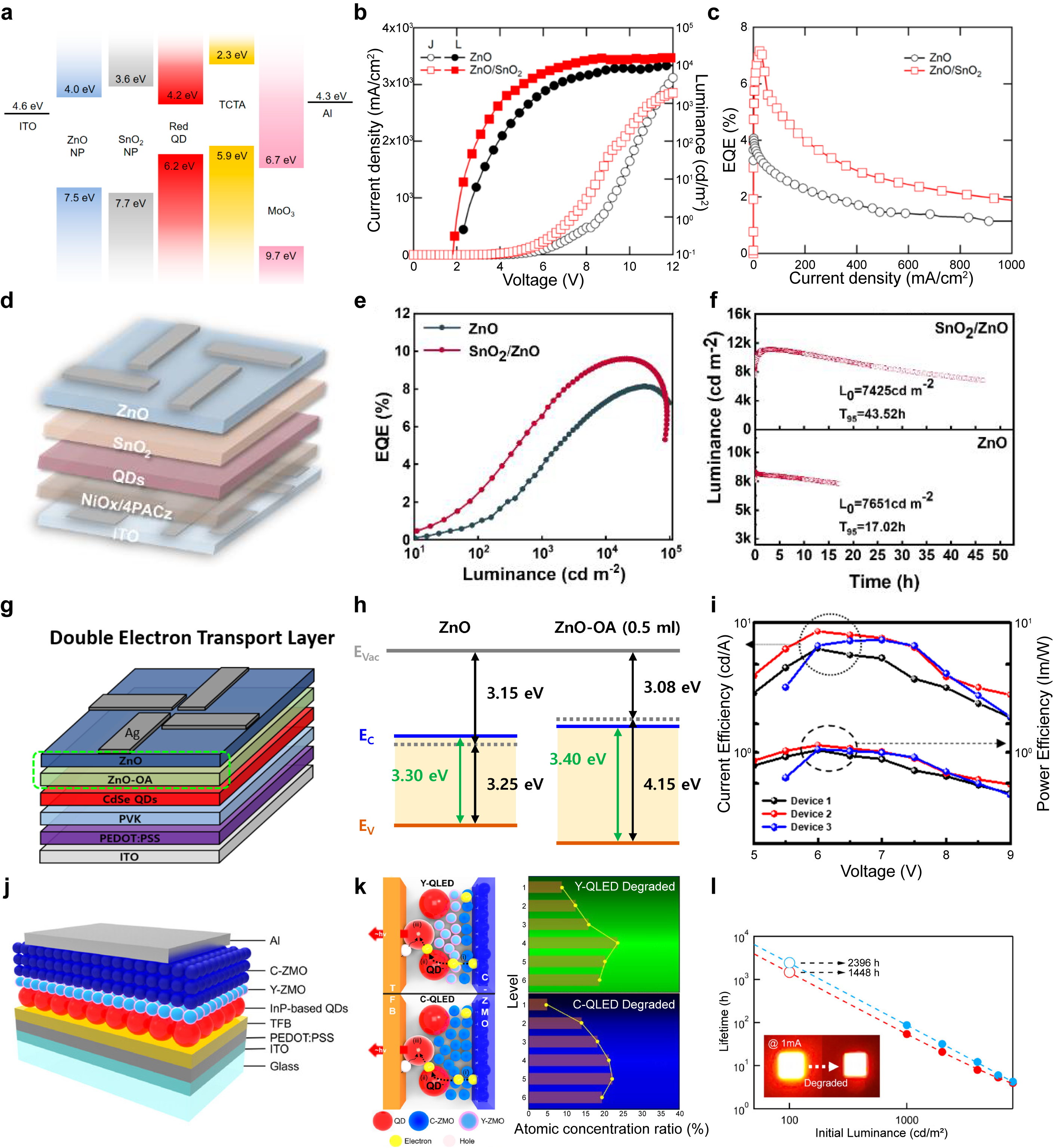
Park et al. introduced a ZnO/SnO2 double metal oxide ETL to mitigate the excessive electron injection and charge imbalance of a single ZnO ETL [48]. Devices with the structure ITO/ZnO/SnO2/red QDs/TCTA/MoO3/Al used 20 nm each of ZnO and SnO2, maintaining the 40 nm total ETL thickness of the reference with a single ZnO layer. The ZnO layer adjacent to ITO provided high electron transport capability, while the SnO2 layer in contact with the QDs restricted spontaneous electron injection from ZnO into the QD layer. Because the conduction band levels of ZnO and the QDs are similar, at 4.0 and 4.2 eV, respectively, electrons can transfer from ZnO into the QDs even without an applied bias, charging the QD layer negatively. The conduction band level of SnO2, at 3.6 eV, forms a larger energy offset with the QDs and suppresses this transfer (Figure 5a). In the current density–voltage–luminance characteristics, the double ETL device showed lower turn-on and operating voltages and steeper increases in both current density and luminance than the single ZnO device (Figure 5b). At 5 V, the current density increased from 33.70 mA cm−2 to 80.44 mA cm−2 and the luminance increased from 848 to 3061 cd m−2. SnO2 does not simply reduce the overall current, as an insulating barrier would. It suppresses unnecessary spontaneous electron injection while maintaining electron transport under operating bias. The maximum EQE increased from 4.11% to 7.16% (Figure 5c), the maximum current efficiency improved by approximately 1.66-fold, from 3.20 to 5.31 cd A−1, and the maximum power efficiency increased from 3.86 to 4.32 lm W−1.
Figure 5.
Double-layer ETL strategies for QLEDs. (a) Energy-level diagram of the ZnO/SnO2 double-ETL device. (b) J–V–L characteristics. (c) EQE as a function of current density. (d) Structure of the all-inorganic QLED employing a SnO2/ZnO double ETL. (e) EQE–luminance characteristics of the ZnO and SnO2/ZnO devices. (f) Operational luminance decay and T95 lifetime. (g) QLED structure employing a ZnO-OA/ZnO double ETL. (h) Energy levels of ZnO and ZnO-OA prepared with 0.5 mL OA. (i) Current and power efficiencies of Device 1 with a single ZnO ETL, Device 2 with a ZnO-OA (0.5 mL)/ZnO double ETL, and Device 3 with a ZnO-OA (1.0 mL)/ZnO double ETL. (j) Schematic device structure of QLEDs employing Y-ZMO/C-ZMO bilayer ETLs. (k) Schematic of Mg ion migration and depth-dependent atomic concentration profiles in degraded QLEDs. (l) Operational lifetime as a function of initial luminance. Adapted from: (a–c) Park et al. [48] (© The Authors 2020, CC BY 4.0); (d–f) Shi et al. [49] (© The Authors 2024, CC BY 4.0); (g–i) Lee et al. [50] (© The Authors 2022, CC BY 4.0); (j–l) Choi et al. [51] (© The Authors 2025, CC BY 4.0).
Shi et al. introduced a SnO2/ZnO double ETL to address interfacial exciton quenching and aging in all-inorganic QLEDs containing ZnO [49]. Devices were fabricated with the structure ITO/NiOx/[4-(9H-carbazol-9-yl)butyl]phosphonic acid/QDs/SnO2/ZnO/Al, in which the SnO2 layer in direct contact with the QDs stabilized the interface, while the upper ZnO layer maintained efficient electron transport (Figure 5d). ZnO had a high electron mobility of 2.74 × 10⁻³ cm2 V−1 s−1 but relatively strong defect related emission and QD exciton quenching, whereas SnO2 had a lower electron mobility of 1.43 × 10⁻³ cm2 V−1 s−1 but a lower defect density and less interfacial nonradiative recombination. Stacking the two materials combined the transport capability of ZnO with the low interfacial defect density and high stability of SnO2. The SnO2/ZnO device maintained a turn-on voltage similar to that of the single ZnO device while reaching a high luminance approaching 105 cd m−2, and its peak EQE increased from 8.1% for the single ZnO layer to approximately 9.6% (Figure 5e). The SnO2 layer prevented direct contact between the QDs and ZnO, reducing interfacial electron transfer and exciton quenching, while the ZnO layer maintained electron transport from the electrode. Rather than simply suppressing electron injection, the double ETL divided the functions between the two layers to regulate charge injection and interfacial recombination simultaneously. The benefit of the double ETL was even more pronounced in operational stability. At comparable initial luminances of 7.43 × 10³ and 7.65 × 10³ cd m−2, the time to 95% of the initial luminance was 43.52 h for the SnO2/ZnO device, approximately 2.6 times the 17.02 h of the ZnO device (Figure 5f). The luminance-decay measurements were performed at a constant current density of 65 mA cm−2. The devices were encapsulated inside a nitrogen-filled glovebox using glass covers and UV-curable NOA61 resin, whereas the subsequent lifetime-test atmosphere and quantitative encapsulation performance were not reported. The ZnO device showed pronounced positive aging followed by negative aging during early storage, whereas the SnO2/ZnO device maintained a relatively stable peak EQE, current density at 8 V, and threshold voltage. The SnO2/ZnO double ETL therefore preserved the high electron mobility of ZnO while suppressing defect mediated quenching and aging behavior at the QD interface, improving both the efficiency and the long-term stability of the all-inorganic QLED.
Lee et al. introduced a double ETL of oleic acid (OA) modified ZnO (ZnO-OA) and ZnO to compensate for the limited hole blocking capability of a single ZnO ETL and the nonuniform QD/ETL interface [50]. Devices were fabricated with the structure ITO/PEDOT:PSS/PVK/QDs/ZnO-OA/ZnO/Ag, in which the ZnO-OA layer adjacent to the QDs regulated energy level alignment and interfacial properties while the upper ZnO layer maintained electron transport from the Ag electrode (Figure 5g). OA modification reduced the work function of ZnO from 3.15 eV to 3.08 and 2.72 eV for ZnO-OA prepared with 0.5 and 1.0 mL of OA, respectively, and shifted the valence band level from approximately 6.40 eV to 7.23 eV (Figure 5h). This shift was attributed to a surface dipole formed by charge transfer from ZnO to the OA ligands. The resulting increase in the hole blocking barrier between the CdSe/ZnS QD layer and the ETL suppressed hole leakage from the QD layer into the ETL, and the OA ligands also reduced ZnO particle aggregation and interfacial roughness, enabling more uniform charge injection. Excessive OA loading, however, restricts electron hopping because of the insulating character of the long hydrocarbon chains. The ZnO-OA (0.5 mL)/ZnO device accordingly achieved a maximum luminance of 27,890 cd m−2 and a maximum current efficiency of 8.57 cd A−1, representing improvements of approximately 9% and 35.6% over the single ZnO ETL (Figure 5i). The ZnO-OA (1.0 mL)/ZnO device also outperformed the single ZnO device, but its higher OA content restricted electron transport and resulted in a lower efficiency than the 0.5 mL condition. The ZnO-OA/ZnO double ETL therefore combined the hole blocking and interface smoothing effects of ZnO-OA with the electron transport capability of ZnO, with the most favorable charge balance obtained at 0.5 mL OA.
Choi et al. proposed a surface passivation strategy using yttrium acetate (Y(Ac)) to suppress Mg ion migration and surface defects in ZMO ETLs [51]. In conventional ZMO, Mg ions can be displaced from the crystal lattice, generating defect sites and subsequently migrating into the QD emissive layer, where they promote nonradiative recombination and device degradation. To address this issue, QLEDs were fabricated with the structure ITO/PEDOT:PSS/TFB/InP-based QDs/Y(Ac)-modified ZMO (Y-ZMO)/control ZMO (C-ZMO)/Al (Figure 5j), in which a 10 nm Y-ZMO layer was inserted adjacent to the QDs, followed by a 30 nm C-ZMO layer. Y(Ac) treatment improve interfacial stability by reducing oxygen vacancies on the ZMO surface and suppressing Mg ion displacement from the lattice. X-ray photoelectron spectroscopy (XPS) depth profiling revealed that Mg ions were redistributed within the ZMO layer and migrated into the QD emissive layer during degradation of the control QLED (C-QLED), whereas such migration was effectively suppressed in the Y-ZMO-based QLED (Y-QLED) (Figure 5k). These results indicate that Y(Ac) passivation suppresses nonradiative recombination by reducing Mg ion migration and the associated formation of interfacial defects. As a result of the improved interfacial stability, the extrapolated T50 at an initial luminance of 100 cd m−2 increased from 1448 h for the C-QLED to 2396 h for the Y-QLED, representing an improvement of approximately 65.5% (Figure 5l). At an initial luminance of 4000 cd m−2, the directly measured T50 values were 19.59 h for the C-QLED and 29.19 h for the 1% Y-QLED. The authors reported an acceleration exponent of 1.44 for lifetime extrapolation and encapsulation using a cover glass. The electrical driving mode, lifetime-test atmosphere, and quantitative barrier performance were not specified. This study demonstrates that controlling not only surface defects but also metal ion migration in ZMO is essential for enhancing the long-term operational stability of QLEDs.
6. Conclusions
ETLs based on metal oxide nanoparticles are key components of QLEDs that determine not only electron injection and transport but also hole blocking, charge balance, and the stability of the QD/ETL interface. ZnO NPs remain the representative material because of their electrical properties and solution processability, yet excessive electron injection arising from their high electron mobility, together with charge trapping and exciton quenching caused by surface defects, degrades device performance and lifetime. Strategies that control both the amount of electron injection and interfacial properties are therefore more important than simply increasing ETL conductivity.
Doping and alloying tune the CBM, Fermi level, carrier concentration, and defect distribution of ZnO and ZMO to establish electron injection conditions appropriate for a given QD composition. However, device performance is not determined by energy level alignment alone. Hole blocking capability, film morphology, and interfacial trap states also govern it as well. Approaches that directly control the electronic states of nanocrystals, such as in situ reductive n-doping, further show that electron transport and device stability are improved while erratic positive aging is suppressed.
Interfacial exciton quenching is influenced not only by defects in metal oxide ETLs but also by organic ligands bound to the QD surface. Oleic acid (OA)-derived ligands passivate surface defects by coordinating with metal ions on QDs, while their long hydrocarbon chains also affect charge transfer at the QD/ETL interface. Undercoordinated metal sites and hydroxyl groups on ZnO and ZMO surfaces may interact with nearby carboxylate ligands through coordination or hydrogen bonding, potentially inducing ligand rearrangement or partial desorption and affecting nonradiative recombination. Alcohol treatment removes surface hydroxyl groups from ZMO, whereas fluorine treatment passivates oxygen vacancy-related defects in ZnO, thereby modifying the chemical environment at the QD/ETL interface. Chen et al. further reported that ethanol molecules bound to ZnO can induce interfacial exciton quenching, while replacing them with electrochemically stable alkali carboxylates improves QLED efficiency and operational stability [52]. These findings indicate that both surface defects and ligand interactions should be considered when optimizing the chemical stability of the QD/ETL interface.
Interlayers and double-layer ETLs modulate electron flux and interfacial properties structurally, without changing the ETL material itself. PMMA, arginine, and PVPy interlayers suppressed excessive electron injection and prevented direct ZnO/QD contact, but excessive thickness or concentration restricted electron transport. The thickness, concentration, position, and number of stacked layers matter as much as the choice of material. Double-layer ETLs avoid this trade-off by assigning high electron mobility to one layer and charge injection, hole blocking, or interfacial stability to the other. The ZnO/SnO2, SnO2/ZnO, and ZnO-OA/ZnO architectures controlled spontaneous electron injection, interfacial quenching and aging, and hole leakage, respectively.
These ETL engineering strategies are also important for improving the efficiency and operational stability of blue QLEDs, which are essential for realizing full-color displays. For example, Da et al. demonstrated that Sn4+/Mg2+ co-doped ZnO ETLs improved both the efficiency and operational lifetime of blue QLEDs by suppressing excessive electron injection and reducing interfacial defects. Similarly, doping can regulate electron transport properties and energy levels, while surface treatment can suppress defect-induced nonradiative recombination. Interlayer insertion and double-layer ETL design can further improve charge balance by controlling electron injection and interfacial properties. Therefore, optimizing these four strategies for blue QLEDs could enhance both efficiency and operational stability by reducing charge accumulation and exciton quenching, and could contribute to the commercialization of full-color QLED displays.
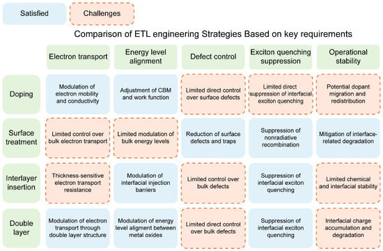
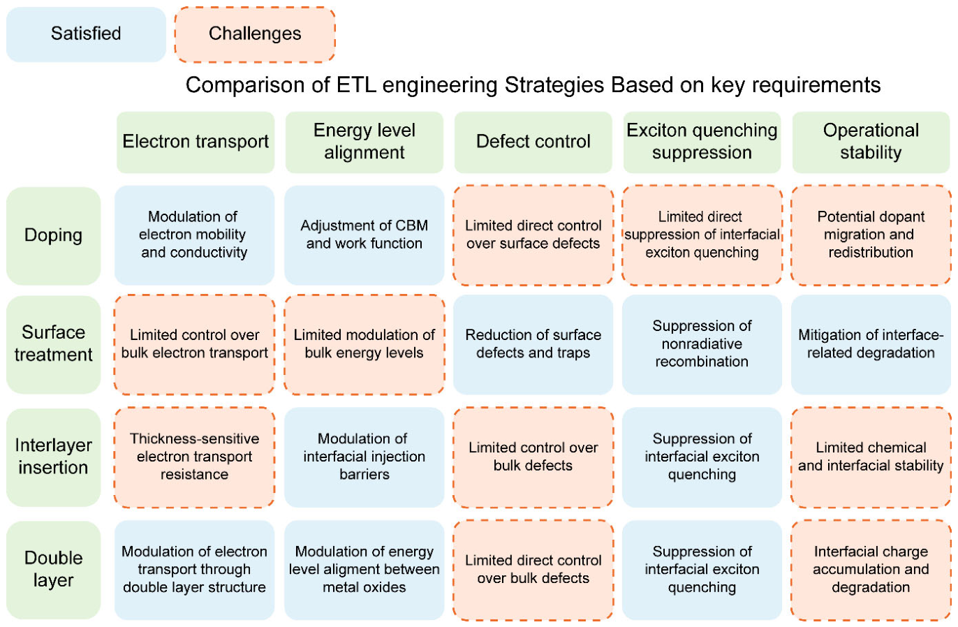
In summary, the central design principle for ETLs based on metal oxide nanoparticles in high-performance QLEDs is not to maximize electron injection but to achieve appropriate electron transport, effective hole blocking, low defect density, and a stable QD/ETL interface simultaneously (Figure 6). Future progress will require synthetic methods that control ETL compositions and surface states, operando characterization capable of tracking charge accumulation and chemical evolution during device operation, and reproducible low temperature solution processing suitable for large area fabrication. Such an integrated approach will provide a foundation for improving QLED efficiency and operational lifetime while suppressing efficiency roll-off, and for implementing these ETLs in practical displays.
Figure 6.
Comparison of ETL engineering strategies based on key requirements for QLEDs. Blue boxes indicate requirements that each strategy satisfies, and orange dashed boxes indicate challenges that require further research.
Author Contributions
H.K. and T.K. wrote the main contents of this manuscript under the supervision of S.L. This study was conducted based on the contributions of all authors. All authors have read and agreed to the published version of the manuscript.
Funding
This work was supported by the Korea Institute for Advancement of Technology (KIAT) grant funded by the Korean Government (Ministry of Education) (P0028101, Semiconductor Specialized University). This work was supported by the National Research Foundation of Korea Grant funded by the Korean Government (MIST) (NRF-2018R1A6A1A03025761 and RS-2026-25587567).
Data Availability Statement
No new data were created or analyzed in this study. Data sharing is not applicable to this article.
Conflicts of Interest
The authors declare no conflicts of interest.
References
- Chen, Z.; Li, H.; Yuan, C.; Gao, P.; Su, Q.; Chen, S. Color Revolution: Prospects and Challenges of Quantum-Dot Light-Emitting Diode Display Technologies. Small Methods 2024, 8, 2300359. [Google Scholar] [CrossRef] [Scilit] [PubMed]
- Kim, T.-H.; Cho, K.-S.; Lee, E.K.; Lee, S.Y.; Chae, J.; Kim, J.W.; Kim, D.H.; Kwon, J.-Y.; Amaratunga, G.; Choi, B.L.; et al. Full-colour quantum dot displays fabricated by transfer printing. Nat. Photonics 2011, 5, 176–182. [Google Scholar] [CrossRef] [Scilit]
- Yang, Y.; Zheng, Y.; Cao, W.; Titov, A.; Hyvonen, J.; Manders, J.R.; Xue, J.; Holloway, P.H.; Qian, L. High-efficiency light-emitting devices based on quantum dots with tailored nanostructures. Nat. Photonics 2015, 9, 259–266. [Google Scholar] [CrossRef] [Scilit]
- Shen, H.; Gao, Q.; Zhang, Y.; Lin, Y.; Lin, Q.; Li, Z.; Chen, L.; Zeng, Z.; Li, X.; Jia, Y.; et al. Visible quantum dot light-emitting diodes with simultaneous high brightness and efficiency. Nat. Photonics 2019, 13, 192–197. [Google Scholar] [CrossRef] [Scilit]
- Sun, Y.; Jiang, Y.; Sun, X.W.; Zhang, S.; Chen, S. Beyond OLED: Efficient Quantum Dot Light-Emitting Diodes for Display and Lighting Application. Chem. Rec. 2019, 19, 1729–1752. [Google Scholar] [CrossRef] [Scilit] [PubMed]
- Won, Y.-H.; Cho, O.; Kim, T.; Chung, D.Y.; Kim, T.; Chung, H.; Jang, H.; Lee, J.; Kim, D.; Jang, E. Highly efficient and stable InP/ZnSe/ZnS quantum dot light-emitting diodes. Nature 2019, 575, 634–638. [Google Scholar] [CrossRef] [Scilit] [PubMed]
- Deng, Y.; Lin, X.; Fang, W.; Di, D.; Wang, L.; Friend, R.H.; Peng, X.; Jin, Y. Deciphering exciton-generation processes in quantum-dot electroluminescence. Nat. Commun. 2020, 11, 2309. [Google Scholar] [CrossRef] [Scilit] [PubMed]
- Yoon, S.-Y.; Lee, Y.-J.; Yang, H.; Jo, D.-Y.; Kim, H.-M.; Kim, Y.; Park, S.M.; Park, S.; Yang, H. Performance Enhancement of InP Quantum Dot Light-Emitting Diodes via a Surface-Functionalized ZnMgO Electron Transport Layer. ACS Energy Lett. 2022, 7, 2247–2255. [Google Scholar] [CrossRef] [Scilit]
- Ding, K.; Chen, H.; Fan, L.; Wang, B.; Huang, Z.; Zhuang, S.; Hu, B.; Wang, L. Polyethylenimine Insulativity-Dominant Charge-Injection Balance for Highly Efficient Inverted Quantum Dot Light-Emitting Diodes. ACS Appl. Mater. Interfaces 2017, 9, 20231–20238. [Google Scholar] [CrossRef] [Scilit] [PubMed]
- Zhang, H.; Sui, N.; Chi, X.; Wang, Y.; Liu, Q.; Zhang, H.; Ji, W. Ultrastable Quantum-Dot Light-Emitting Diodes by Suppression of Leakage Current and Exciton Quenching Processes. ACS Appl. Mater. Interfaces 2016, 8, 31385–31391. [Google Scholar] [CrossRef] [Scilit] [PubMed]
- Jin, H.; Moon, H.; Lee, W.; Hwangbo, H.; Yong, S.H.; Chung, H.K.; Chae, H. Charge balance control of quantum dot light emitting diodes with atomic layer deposited aluminum oxide interlayers. RSC Adv. 2019, 9, 11634–11640. [Google Scholar] [CrossRef] [Scilit] [PubMed]
- Wang, Y.-K.; Wan, H.; Xu, J.; Zhong, Y.; Jung, E.D.; Park, S.M.; Teale, S.; Imran, M.; Yu, Y.-J.; Xia, P.; et al. Bifunctional Electron-Transporting Agent for Red Colloidal Quantum Dot Light-Emitting Diodes. J. Am. Chem. Soc. 2023, 145, 6428–6433. [Google Scholar] [CrossRef] [Scilit] [PubMed]
- Dai, X.; Zhang, Z.; Jin, Y.; Niu, Y.; Cao, H.; Liang, X.; Chen, L.; Wang, J.; Peng, X. Solution-processed, high-performance light-emitting diodes based on quantum dots. Nature 2014, 515, 96–99. [Google Scholar] [CrossRef] [Scilit] [PubMed]
- Kim, J. Recent progresses and challenges in colloidal quantum dot light-emitting diodes: A focus on electron transport layers with metal oxide nanoparticles and organic semiconductors. Nanoscale Horiz. 2024, 9, 2167–2197. [Google Scholar] [CrossRef] [Scilit] [PubMed]
- Mashford, B.S.; Stevenson, M.; Popovic, Z.; Hamilton, C.; Zhou, Z.; Breen, C.; Steckel, J.; Bulovic, V.; Bawendi, M.; Coe-Sullivan, S.; et al. High-efficiency quantum-dot light-emitting devices with enhanced charge injection. Nat. Photonics 2013, 7, 407–412. [Google Scholar] [CrossRef] [Scilit]
- Colvin, V.L.; Schlamp, M.C.; Alivisatos, A.P. Light-emitting diodes made from cadmium selenide nanocrystals and a semiconducting polymer. Nature 1994, 370, 354–357. [Google Scholar] [CrossRef] [Scilit]
- Anikeeva, P.O.; Madigan, C.F.; Halpert, J.E.; Bawendi, M.G.; Bulović, V. Electronic and excitonic processes in light-emitting devices based on organic materials and colloidal quantum dots. Phys. Rev. B 2008, 78, 085434. [Google Scholar] [CrossRef] [Scilit]
- Coe, S.; Woo, W.-K.; Bawendi, M.; Bulović, V. Electroluminescence from single monolayers of nanocrystals in molecular organic devices. Nature 2002, 420, 800–803. [Google Scholar] [CrossRef] [Scilit] [PubMed]
- Dabbousi, B.O.; Rodriguez-Viejo, J.; Mikulec, F.V.; Heine, J.R.; Mattoussi, H.; Ober, R.; Jensen, K.F.; Bawendi, M.G. (CdSe)ZnS Core−Shell Quantum Dots: Synthesis and Characterization of a Size Series of Highly Luminescent Nanocrystallites. J. Phys. Chem. B 1997, 101, 9463–9475. [Google Scholar] [CrossRef] [Scilit]
- Sun, Q.; Wang, Y.A.; Li, L.S.; Wang, D.; Zhu, T.; Xu, J.; Yang, C.; Li, Y. Bright, multicoloured light-emitting diodes based on quantum dots. Nat. Photonics 2007, 1, 717–722. [Google Scholar] [CrossRef] [Scilit]
- Terao, J.; Wadahama, A.; Matono, A.; Tada, T.; Watanabe, S.; Seki, S.; Fujihara, T.; Tsuji, Y. Design principle for increasing charge mobility of π-conjugated polymers using regularly localized molecular orbitals. Nat. Commun. 2013, 4, 1691. [Google Scholar] [CrossRef] [Scilit] [PubMed]
- Turak, A. Interfacial degradation in organic optoelectronics. RSC Adv. 2013, 3, 6188–6225. [Google Scholar] [CrossRef] [Scilit]
- Cho, K.-S.; Lee, E.K.; Joo, W.-J.; Jang, E.; Kim, T.-H.; Lee, S.J.; Kwon, S.-J.; Han, J.Y.; Kim, B.-K.; Choi, B.L.; et al. High-performance crosslinked colloidal quantum-dot light-emitting diodes. Nat. Photonics 2009, 3, 341–345. [Google Scholar] [CrossRef] [Scilit]
- Caruge, J.M.; Halpert, J.E.; Wood, V.; Bulović, V.; Bawendi, M.G. Colloidal quantum-dot light-emitting diodes with metal-oxide charge transport layers. Nat. Photonics 2008, 2, 247–250. [Google Scholar] [CrossRef] [Scilit]
- Kim, H.Y.; Park, Y.J.; Kim, J.; Han, C.J.; Lee, J.; Kim, Y.; Greco, T.; Ippen, C.; Wedel, A.; Ju, B.; et al. Transparent InP Quantum Dot Light-Emitting Diodes with ZrO2 Electron Transport Layer and Indium Zinc Oxide Top Electrode. Adv. Funct. Mater. 2016, 26, 3454–3461. [Google Scholar] [CrossRef] [Scilit]
- Lee, K.; Lee, J.; Bae, Y.; Roh, H.; Jung, W.H.; Lim, J.; Kim, J.; Roh, J. Interfacial Modification of ZnO/ZnMgO Bilayer for Efficient and Stable InP Quantum Dot Light-Emitting Diodes via Ultraviolet Ozone Treatment. ACS Appl. Mater. Interfaces 2024, 16, 55658–55665. [Google Scholar] [CrossRef] [Scilit] [PubMed]
- Wood, V.; Panzer, M.J.; Halpert, J.E.; Caruge, J.-M.; Bawendi, M.G.; Bulović, V. Selection of Metal Oxide Charge Transport Layers for Colloidal Quantum Dot LEDs. ACS Nano 2009, 3, 3581–3586. [Google Scholar] [CrossRef] [Scilit] [PubMed]
- Stouwdam, J.W.; Janssen, R.A.J. Red, green, and blue quantum dot LEDs with solution processable ZnO nanocrystal electron injection layers. J. Mater. Chem. 2008, 18, 1889–1894. [Google Scholar] [CrossRef] [Scilit]
- Cao, S.; Zheng, J.; Zhao, J.; Yang, Z.; Li, C.; Guan, X.; Yang, W.; Shang, M.; Wu, T. Enhancing the Performance of Quantum Dot Light-Emitting Diodes Using Room-Temperature-Processed Ga-Doped ZnO Nanoparticles as the Electron Transport Layer. ACS Appl. Mater. Interfaces 2017, 9, 15605–15614. [Google Scholar] [CrossRef] [Scilit] [PubMed]
- Kwak, J.; Bae, W.K.; Lee, D.; Park, I.; Lim, J.; Park, M.; Cho, H.; Woo, H.; Yoon, D.Y.; Char, K.; et al. Bright and Efficient Full-Color Colloidal Quantum Dot Light-Emitting Diodes Using an Inverted Device Structure. Nano Lett. 2012, 12, 2362–2366. [Google Scholar] [CrossRef] [Scilit] [PubMed]
- Qian, L.; Zheng, Y.; Xue, J.; Holloway, P.H. Stable and efficient quantum-dot light-emitting diodes based on solution-processed multilayer structures. Nat. Photonics 2011, 5, 543–548. [Google Scholar] [CrossRef] [Scilit]
- Cao, W.; Xiang, C.; Yang, Y.; Chen, Q.; Chen, L.; Yan, X.; Qian, L. Highly stable QLEDs with improved hole injection via quantum dot structure tailoring. Nat. Commun. 2018, 9, 2608. [Google Scholar] [CrossRef] [Scilit] [PubMed]
- Bae, W.K.; Park, Y.-S.; Lim, J.; Lee, D.; Padilha, L.A.; McDaniel, H.; Robel, I.; Lee, C.; Pietryga, J.M.; Klimov, V.I. Controlling the influence of Auger recombination on the performance of quantum-dot light-emitting diodes. Nat. Commun. 2013, 4, 2661. [Google Scholar] [CrossRef] [Scilit] [PubMed]
- Fan, J.; Han, C.; Yang, G.; Song, B.; Xu, R.; Xiang, C.; Zhang, T.; Qian, L. Recent Progress of Quantum Dots Light-Emitting Diodes: Materials, Device Structures, and Display Applications. Adv. Mater. 2024, 36, 2312948. [Google Scholar] [CrossRef] [Scilit] [PubMed]
- Alexandrov, A.; Zvaigzne, M.; Lypenko, D.; Nabiev, I.; Samokhvalov, P. Al-, Ga-, Mg-, or Li-doped zinc oxide nanoparticles as electron transport layers for quantum dot light-emitting diodes. Sci. Rep. 2020, 10, 7496. [Google Scholar] [CrossRef] [Scilit] [PubMed]
- Zhang, B.; Luo, Y.; Mai, C.; Mu, L.; Li, M.; Wang, J.; Xu, W.; Peng, J. Effects of ZnMgO Electron Transport Layer on the Performance of InP-Based Inverted Quantum Dot Light-Emitting Diodes. Nanomaterials 2021, 11, 1246. [Google Scholar] [CrossRef] [Scilit] [PubMed]
- Zheng, Y.; Lin, X.; Li, J.; Chen, J.; Wu, W.; Song, Z.; Gao, Y.; Hu, Z.; Wang, H.; Ye, Z.; et al. In situ n-doped nanocrystalline electron-injection-layer for general-lighting quantum-dot LEDs. Nat. Commun. 2025, 16, 3362. [Google Scholar] [CrossRef] [Scilit] [PubMed]
- Da, C.; Xie, L.; Wang, W.; Wang, T.; Yi, Y.-Q.; Zhuang, J.; Meng, X.; Su, W.; Yu, T.; Cui, Z. Microfluidic-synthesized Sn4+/Mg2+ co-doped zinc oxide for highly efficient and stable blue ZnSeTe QLEDs. Nano Res. 2026, 19, 94908518. [Google Scholar] [CrossRef] [Scilit]
- Liu, M.; Lin, C.; Zhang, H.; Shi, X.; Zeng, R.; Pan, D. Tailored SnO2 electron transport layer delivers over 27% external quantum efficiency in quantum dot light-emitting diodes compatible with multiple hole transport layers. Nano Res. 2026, 19, 94908720. [Google Scholar] [CrossRef] [Scilit]
- Chung, D.S.; Davidson-Hall, T.; Cotella, G.; Lyu, Q.; Chun, P.; Aziz, H. Significant Lifetime Enhancement in QLEDs by Reducing Interfacial Charge Accumulation via Fluorine Incorporation in the ZnO Electron Transport Layer. Nano-Micro Lett. 2022, 14, 212. [Google Scholar] [CrossRef] [Scilit] [PubMed]
- Oh, S.; Choi, J.; Park, J.; Choi, Y.K.; Park, T.; Ali, A.; Ahn, J.; Kim, J.; Oh, S.J. Surface passivation engineering for stable optoelectronic devices via hydroxyl-free ZnMgO nanoparticles. Nano Converg. 2025, 12, 28. [Google Scholar] [CrossRef] [Scilit] [PubMed]
- Chrzanowski, M.; Zatryb, G.; Sitarek, P.; Podhorodecki, A. Effect of Air Exposure of ZnMgO Nanoparticle Electron Transport Layer on Efficiency of Quantum-Dot Light-Emitting Diodes. ACS Appl. Mater. Interfaces 2021, 13, 20305–20312. [Google Scholar] [CrossRef] [Scilit] [PubMed]
- Liu, H.; Gao, P.-L.; Song, Y.-M.; Wang, M.-W.; Ding, T.; Jiang, J.; Zheng, R.-F.; Chen, S.; Ng, K.-W.; Wang, S.-P. Chlorine-Modified Low-Temperature Crystallized TiO2 Electron Transport Layer for Stable QLEDs. ACS Appl. Electron. Mater. 2025, 7, 11142–11148. [Google Scholar] [CrossRef] [Scilit]
- Zvaigzne, M.; Alexandrov, A.; Tkach, A.; Lypenko, D.; Nabiev, I.; Samokhvalov, P. Optimizing the PMMA Electron-Blocking Layer of Quantum Dot Light-Emitting Diodes. Nanomaterials 2021, 11, 2014. [Google Scholar] [CrossRef] [Scilit] [PubMed]
- Chae, Y.-B.; Kim, S.-Y.; Choi, H.-D.; Moon, D.-G.; Lee, K.-H.; Kim, C.-K. Enhancing Efficiency in Inverted Quantum Dot Light-Emitting Diodes through Arginine-Modified ZnO Nanoparticle Electron Injection Layer. Nanomaterials 2024, 14, 266. [Google Scholar] [CrossRef] [Scilit] [PubMed]
- Kiguye, C.; Jeong, W.J.; Jeong, G.H.; Park, J.H.; Kwak, H.J.; Kim, G.W.; Jang, S.H.; Kim, J.Y. Single, Double and ETL-Sandwiched PVPy Interlayer Effect on Charge Injection Balance and Performance of Inverted Quantum Dot Light-Emitting Diodes. Polymers 2023, 15, 3308. [Google Scholar] [CrossRef] [Scilit] [PubMed]
- Wang, L.; Li, G.; Xiang, R.; Wu, H.; Huang, Z.; Huang, S.; Tang, Z.; Guo, X.; Pan, D.; Zhang, H.; et al. Over 30% efficient and highly stable Co-SnO2 -based QLEDs through ultrathin MgCl2 interface engineering. Nano Res. 2026, 19, 94909019. [Google Scholar] [CrossRef] [Scilit]
- Park, M.; Roh, J.; Lim, J.; Lee, H.; Lee, D. Double Metal Oxide Electron Transport Layers for Colloidal Quantum Dot Light-Emitting Diodes. Nanomaterials 2020, 10, 726. [Google Scholar] [CrossRef] [Scilit] [PubMed]
- Shi, H.; Ren, Z.; Zhou, X.; Ji, H.; Zhang, Y.; Chen, Y. Stable and efficient all-inorganic quantum dot light-emitting diodes based on a double-layer electron transport layer. J. Phys. Conf. Ser. 2024, 2827, 012001. [Google Scholar] [CrossRef] [Scilit]
- Lee, D.Y.; Kim, H.H.; Noh, J.-H.; Lim, K.-Y.; Park, D.; Lee, I.-H.; Choi, W.K. Enhanced Luminance of CdSe/ZnS Quantum Dots Light-Emitting Diodes Using ZnO-Oleic Acid/ZnO Quantum Dots Double Electron Transport Layer. Nanomaterials 2022, 12, 2038. [Google Scholar] [CrossRef] [Scilit] [PubMed]
- Choi, H.; Shin, D.; Bae, W.K.; Lee, H. Enhanced Stability of Cd-Free Quantum Dot Light-Emitting Diodes via Yttrium Acetate-Modified ZnMgO: Suppressing Mg Migration. Adv. Opt. Mater. 2025, 13, 2500988. [Google Scholar] [CrossRef] [Scilit]
- Chen, D.; Ma, L.; Chen, Y.; Zhou, X.; Xing, S.; Deng, Y.; Hao, Y.; Pu, C.; Kong, X.; Jin, Y. Electrochemically Stable Ligands of ZnO Electron-Transporting Layers for Quantum-Dot Light-Emitting Diodes. Nano Lett. 2023, 23, 1061–1067. [Google Scholar] [CrossRef] [Scilit] [PubMed]
Disclaimer/Publisher’s Note: The statements, opinions and data contained in all publications are solely those of the individual author(s) and contributor(s) and not of MDPI and/or the editor(s). MDPI and/or the editor(s) disclaim responsibility for any injury to people or property resulting from any ideas, methods, instructions or products referred to in the content. |
© 2026 by the authors. Licensee MDPI, Basel, Switzerland. This article is an open access article distributed under the terms and conditions of the Creative Commons Attribution (CC BY) license.