


Abstract
Diffractive optical elements (DOEs) have become core components for converting Gaussian beams into flat-top beams due to their advantages of flexible design, compact size, and precise control over light field distribution. However, during the fabrication of multi-step DOEs, some processes such as ion beam etching tend to produce etching depth errors, which cause deviations of the surface micro–nano phase structures from the designed values and thus severely degrade the beam shaping performance. This paper proposes a focusing DOE for flat-top beam shaping, which combines the focusing phase with the phase optimized by the weighted constraint iterative algorithm to establish a phase distribution resilient to etching depth errors. Thus, the proposed focusing DOE exhibits significantly improved robustness to etching depth errors and effectively reduces the structural complexity of laser optical systems. Our experimental results show that the designed DOE can stably convert the incident Gaussian beam into flat-top beams within the etching depth error range of ±30 nm, with both the flat-top beam uniformity and diffraction efficiency above 95%, and the maximum tolerable etching depth error reaches ±90 nm.
1. Introduction
In modern optical fields such as laser processing, optical communication, and high-precision optical detection, the spatial intensity distribution of a laser beam directly determines the working accuracy, energy utilization efficiency and operational stability of the system [1,2,3,4]. The Gaussian beam, as the inherent output form of a laser, exhibits a radial Gaussian intensity distribution with high central intensity and rapidly decaying edge intensity. It fails to meet the strict requirements of the above fields for beam uniformity and edge steepness. Moreover, the low-intensity areas on both sides often lead to energy waste, thereby significantly reducing energy efficiency. Therefore, the efficient conversion of Gaussian beams into flat-top beams with uniform intensity has become a key technical support for improving the performance of optical systems. At present, a variety of mature flat-top beam shaping schemes have been developed, including π-Shapers [5,6], deformable mirrors [7] and DOEs [8]. Deformable mirrors can actively modulate optical wavefronts to achieve target intensity distribution, supporting dynamic beam optimization, yet they rely on complicated driving and feedback control systems. The π-Shaper is a typical refractive beam shaper with high laser damage resistance and high efficiency under collimated illumination, whereas its optical performance is sensitive to incident beam conditions and it cannot integrate focusing functionality. Benefiting from unique advantages such as flexible design, compact size, and precise control over the phase, amplitude, and polarization of incident beams, DOEs have gradually replaced traditional refractive optical elements (ROEs) [9,10,11] and DOEs are now widely used in computer-generated holographic displays [12,13], multifunctional optical elements [14], holographic optical data processing [15], and beam shaping [16,17,18]. DOEs possess irreplaceable application advantages in miniaturized and high-precision optical systems, making them the core devices for converting Gaussian beams into flat-top beams [19,20].
In practical engineering applications, the usage of DOEs for flat-top beam shaping usually adopts multi-step phase distributions to generate the required high-precision phase profiles. Multi-step DOEs require advanced lithography techniques, such as electron-beam lithography, multiple steps of photolithography, and reactive ion beam etching, as well as other micro–nano fabrication processes [21,22]. Recently, grayscale lithography has emerged as another attractive manufacturing route [23,24], which can form multilevel relief structures through a single exposure, avoiding repeated lithography and etching cycles, and it can be combined with ion beam etching to achieve high-fidelity pattern transfer. Nevertheless, multi-exposure photolithography still enables precise independent control over each phase step height, making it well suited for fabricating the discrete 16-step DOE studied in this work. However, limited by the precision of processing equipment, the actual etching depth tends to deviate from the designed value. Problems such as degraded uniformity of the output flat-top beam significantly lower the operational stability and reliability of the optical systems.
Niu et al. [25] proposed a polydimethylsiloxane (PDMS)-polymer-based flexible tunable DOE free from ion etching or laser fabrication. However, the flat-top beam generated by this method achieves both efficiency and uniformity below 70%. You et al. [26] proposed 3D-printed glass ternary DOEs that eliminate complex lithography, yet their phase modulation precision is inferior to multi-step etched DOEs and requires further printing optimization. Chen et al. [27] proposed a beam shaping metalens. Its fabrication only requires one-step lithography to prepare a periodic subwavelength nanopillar array on a silicon substrate. However, the uniformity of the obtained flat-top beam is relatively low, with the RMS of circular and square flat-top beams reaching 16% and 24%, respectively. All above lithography-free or simplified fabrication schemes cannot simultaneously realize high uniformity and high efficiency flat-top shaping, which motivates our work to improve error robustness for conventional lithographically processed DOEs.
In this paper, a focusing DOE capable of suppressing the influence of etching depth errors is proposed. Combining the focusing phase with the beam shaping phase optimized by the weighted constraint iterative algorithm, a phase distribution model insensitive to etching depth errors is constructed. This improves the etching depth error robustness of the element, while achieving the dual functions of focusing and beam shaping in a single device, effectively simplifying the complexity of laser optical systems. Numerical simulations and optical experiments are conducted to validate the proposed method. This study can provide a stable and compact beam shaping scheme for high-precision optical systems and promote the further engineering application of DOEs in modern optical fields.
2. Methods
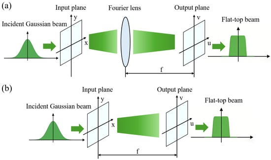
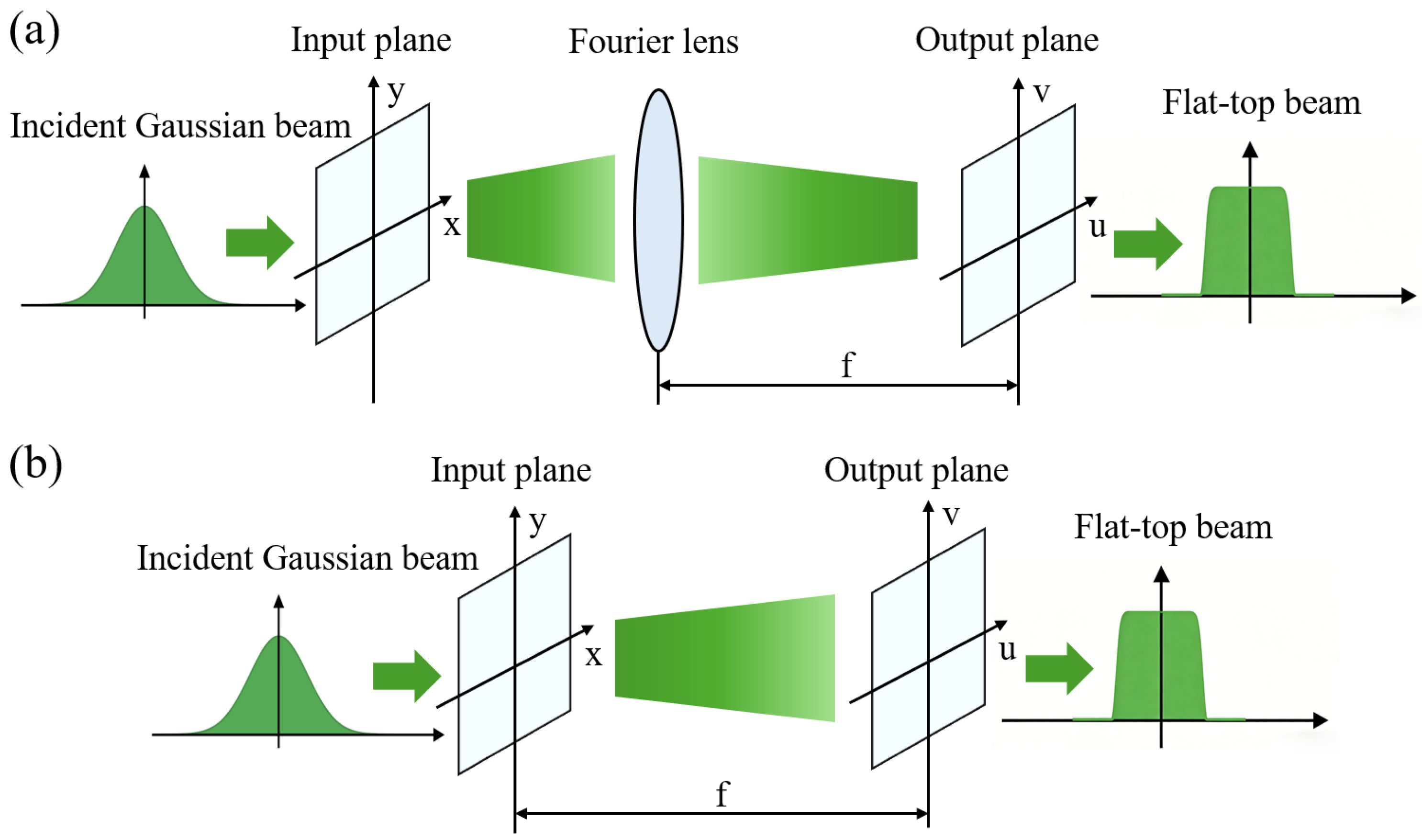
Before introducing the proposed method, we first present the conventional beam shaping optical setup, as shown in Figure 1a. The input plane is located at the front plane of the Fourier lens, and the output plane is at the back focal plane of the Fourier lens. The Gaussian beam incident on the input plane is modulated by the iteratively optimized phase-only distribution, and its intensity distribution is converted into the desired flat-top beam intensity distribution on the output plane after passing through the Fourier lens. In contrast, the proposed beam shaping optical setup eliminates the need for an additional Fourier lens, as illustrated in Figure 1b. Only a single iteratively optimized phase-only distribution integrated with a focusing phase is used to modulate the input Gaussian beam, and the target flat-top intensity distribution can be directly obtained at the output plane. This approach not only improves the robustness of the element to etching depth errors but also effectively simplifies the complexity of the laser optical system.
Figure 1.
(a) Schematic of conventional beam shaping optical path system. (b) Schematic of the proposed beam shaping optical path system.
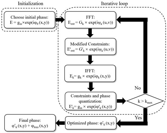
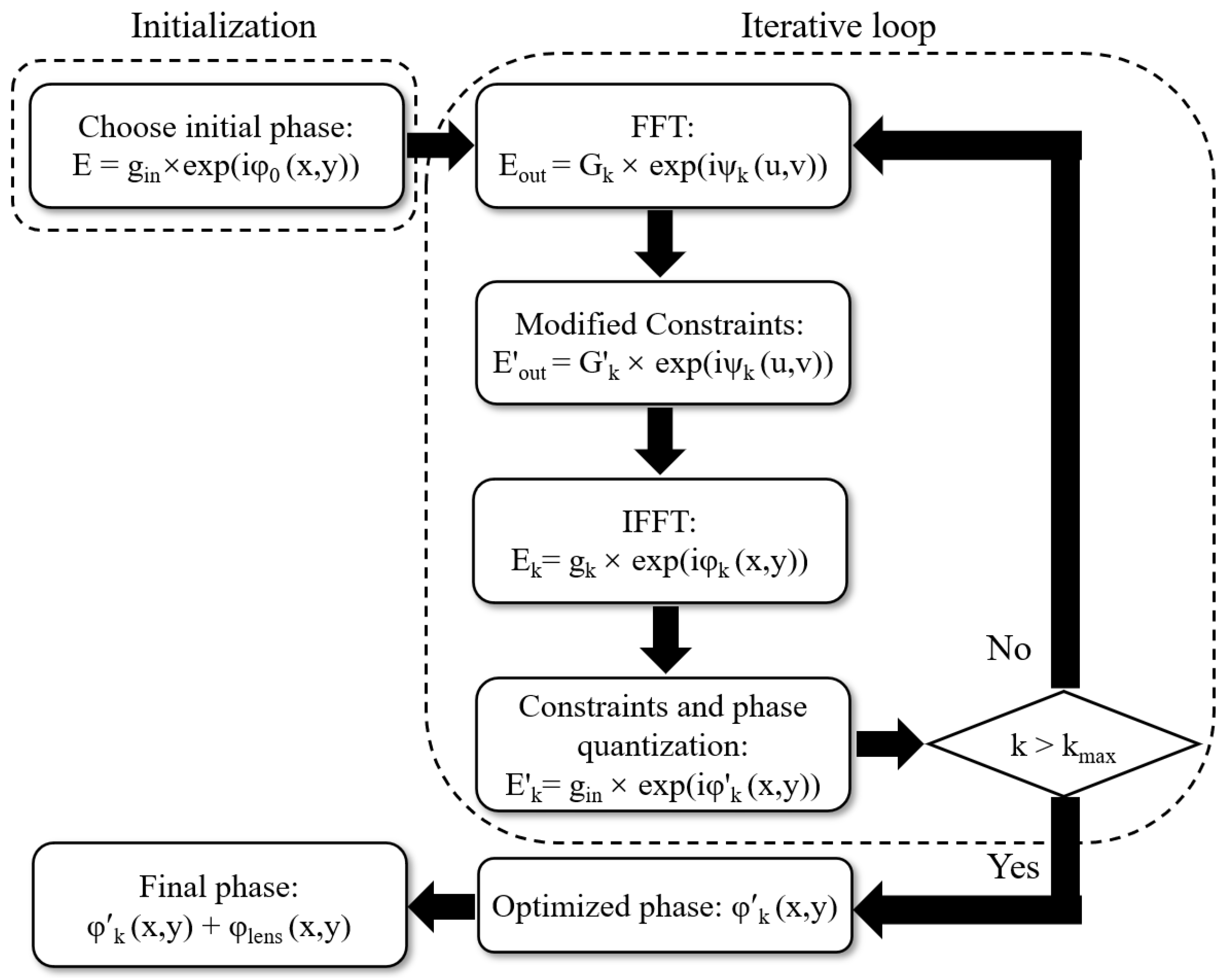
The flowchart of our proposed method is shown in Figure 2. Firstly, we adopt the improved GS algorithm, namely the weighted constrained iterative algorithm. The weighted constrained iterative algorithm needs to divide the signal region and noise region based on the amplitude distribution of the target flat-top beam ut. The area with non-zero amplitude is the signal region (SR), and the area with zero amplitude is the noise region (NR). The input Gaussian beam gin and the initial phase distribution φ0, which adopts a quadratic phase, form the complex amplitude distribution E form the complex amplitude distribution. Then, through Fourier transformation, the complex amplitude distribution Eout is obtained, and the amplitude distribution Gk of Eout is constrained to obtain E’out. Next, the inverse Fourier transformation is performed to obtain Ek, whose amplitude is replaced by the input Gaussian beam gin, and phase φk is quantized into 16 levels to obtain φ’k. This process is repeated until the iteration terminates. Considering that the continuous phase relief needs to be discretized into 16 levels in the actual fabrication of DOEs, we perform phase quantization during the algorithm iteration to reduce the adverse effects caused by discontinuous phase relief introduced by quantization after iterative optimization. An adaptive over-compensation method is adopted for the amplitude constraint at the output plane, which introduces an adaptive parameter βk that varies with the iteration progress. The formula can be expressed as follows [28]:
where ut is the target amplitude distribution, Gk the reconstructed amplitude distribution at the kth iteration, and G’k the modified amplitude distribution at the kth iteration. The initial value of the adaptive parameter β0 is set to a very small number, and we choose 10−8 here.
Figure 2.
Schematic diagram of the weighted constraint iterative algorithm.
It can be seen from Equation (1) that the adaptive over-compensation method constrains the amplitude distribution in the signal region and adopts the adaptive parameter βk to accelerate the convergence speed of the iterative algorithm. When βk is relatively small, the constraint strategy in the signal region is similar to that of the GS algorithm, so the convergence of the iteration process is effective and stable. After multiple iterations, βk will approach 1, and the constraint strategy in the signal region becomes similar to the traditional over-compensation method. In the kth iteration, if the amplitude distribution Gk at some pixels in the signal region is smaller than the target amplitude ut, the enforced amplitude G’k at the corresponding pixels in the (k + 1)th iteration will be amplified to be closer to the target amplitude. After multiple iterations, the discrepancy between the reconstructed amplitude distribution and the target amplitude distribution is reduced.
After obtaining the phase-only distribution upon completion of the iteration, we superimpose the focusing phase onto it. The focusing phase is expressed by the following formula:
Thus, the DOE phase for beam shaping capable of suppressing the influence caused by etching depth errors is obtained, and its formula is as follows:
It is worth noting that the optimized shaping phase φ’k has already been quantized, while the focusing phase φlens is continuous and smooth. Therefore, the composite phase φDOE also needs to be quantified.
Etching depth errors introduce pure phase errors without energy dissipation. Pure phase perturbation only redistributes optical intensity spatially, so the total energy within the target flat-top region remains nearly unchanged, and diffraction efficiency is barely affected. When etching depth errors exist on a shaping-only DOE, local phase mismatches produce undesired non-diffracted stray light components. To realize the far-field beam transformation, an external Fourier lens is indispensable in the optical setup, which optically focuses all stray light into sharp high-intensity hot spots superimposed on the target flat-top profile, drastically reducing beam uniformity. For our proposed composite DOE, the quadratic focusing phase is superimposed onto the shaping phase during design, encoding the Fourier transform function inside the element itself and removing the requirement for an external bulk lens. Stray light induced by identical etching deviations propagates freely without subsequent focusing optics, thus spreading into low-intensity dispersed background noise rather than concentrated bright spots. The destructive interference from fabrication errors is significantly attenuated. Therefore, incorporating the focusing phase, φDOE becomes a phase distribution that is less sensitive to etching depth errors. This not only effectively suppresses the influence of etching depth errors but also realizes the optical transformation without the external lens shown in Figure 1b, providing the flexibility to precisely control beam propagation at different distances in the initial stage and effectively simplifying the complexity of the optical system.
The beam uniformity (U) [29] and energy utilization efficiency (η) [30] are used to evaluate the reconstruction quality of the obtained flat-top beam, and are defined as follows:
where I is the intensity distribution of the reconstructed flat-top beam. The value of U ranges from 0 to 1, and a higher U value indicates better uniformity of the output flat-top beam; the value of η ranges from 0 to 1, and a higher η value indicates higher energy utilization efficiency.
3. Simulation
In this section, numerical simulations are performed to verify the proposed method. The simulation parameters are set as follows: the Gaussian beam is defined as gin = exp [−(x02 + y02)/win2], the target square flat-top beam is defined as ut = exp [−(x20 + y20)/wout20], and the waist radii win and wout are set to 1.6 mm and 0.2 mm, respectively. The incident wavelength λ is set to 532 nm. Both the input and output planes are discretized into a 1024 × 1024 grid, and the sampling interval in the input plane is set to 8 μm. The focal length f of the Fourier lens is 300 mm. The refractive index is set to 1.4607. All phase retrieval processes are run for 100 iterations.
Here, a quadratic phase is adopted as the initial phase. It can eliminate the speckle noise caused by destructive interference between sampling points with random and unstable phase distributions [31]. The quadratic phase is given by the following equation:
where a and b are constant and lie between 0 and 1; x0 and y0 are pixel coordinates; M is the number of pixels occupied by the hologram along the x-axis; d is the width of the reconstruction intensity distributions; Δx is the sampling interval of the reconstruction plane; and w denotes the pixel width corresponding to the waist radius of the incident Gaussian beam.
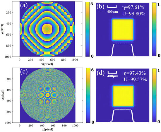
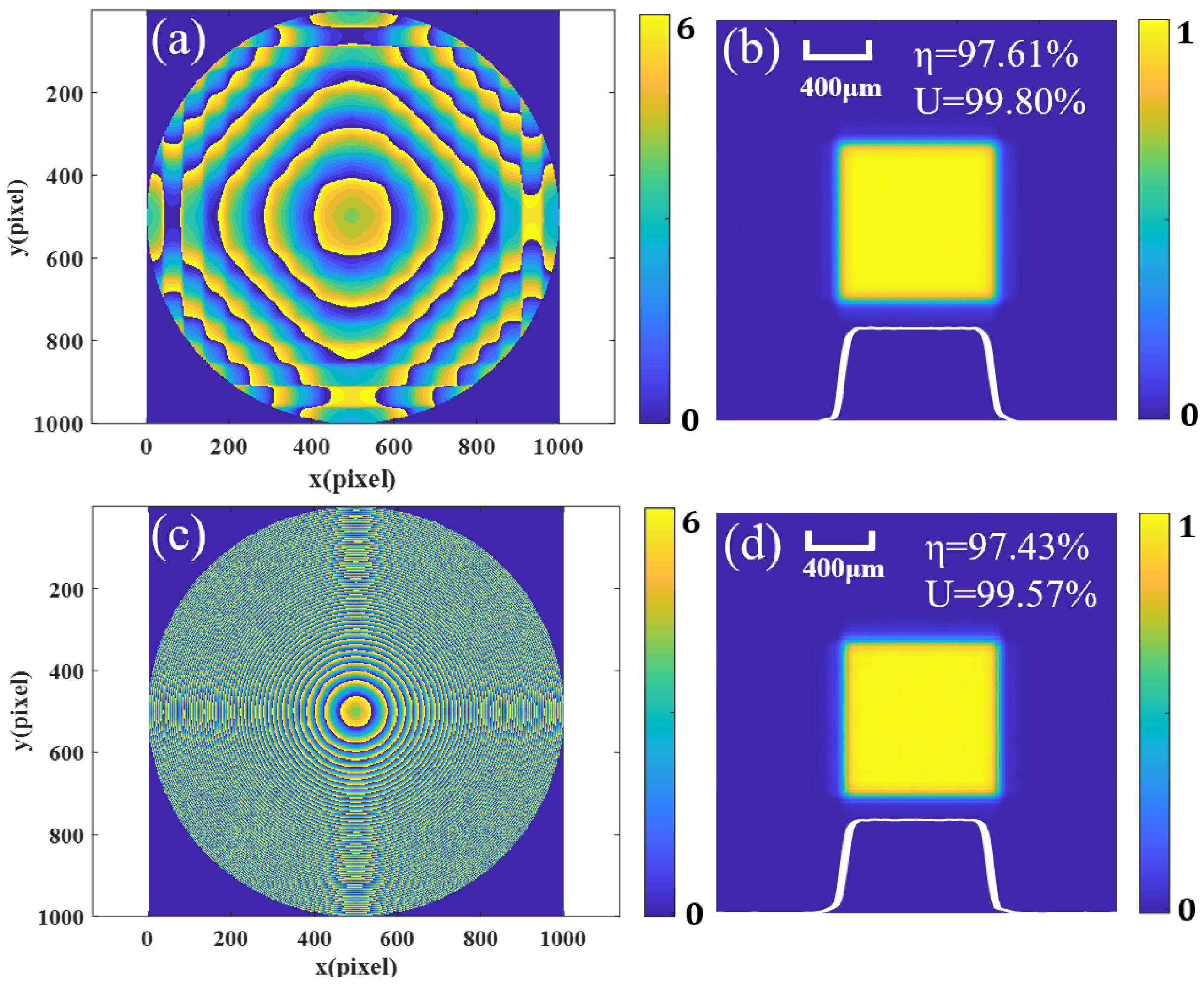
Both the non-focusing DOE phase and the focusing DOEs without introducing etching depth errors, and the corresponding results of beam shaping, are shown in Figure 3. Figure 3a presents the reconstructed phase distribution of the non-focusing DOEs, characterized by slow and smooth phase variation. Figure 3c illustrates the phase distributions of the focusing DOEs, which display dense concentric rings, presenting typical lens phase characteristics. Figure 3b,d show the reconstructed intensity distributions obtained from the non-focusing DOE phase and the focusing DOEs, respectively. It can be seen that both can produce high-quality square flat-top beams, with efficiency and uniformity maintained above 97% and 99%, respectively.
Figure 3.
Phase distributions of square flat-top beam without etching depth errors: (a) non-focusing DOEs, (c) focusing DOEs; reconstructed intensity distributions of square flat-top beam without etching depth errors: (b) non-focusing DOEs, (d) focusing DOEs. The color bars of subplots (a,c) represent the encoded phase value in radians (rad) on the DOE aperture, ranging from 0 to 6 rad. The color bars of subplots (b,d) denote normalized intensity from 0 to 1. The white scale bar at the top represents a length of 400 μm.
The etching errors investigated in this work originate from the reactive ion etching (RIE) fabrication workflow. During lithography and alignment, fluctuations in process parameters including photoresist selection, photoresist pre-baking temperature and duration, exposure dose, and development time lead to pattern transfer deviations. In the subsequent etching stage, imperfect control over process conditions such as etching gas composition, etching duration, and chamber working pressure further causes the actual etching depth to deviate from the designed value.
In the design and fabrication of DOEs, etching depth modulates diffraction by introducing phase differences of light. Accordingly, etching depth errors Δh can be converted into phase errors Δφ. The phase error Δφ corresponding to each etching depth error Δh is governed by Δφ = 2πΔh (n − 1)/λ, and such phase deviations are superimposed onto the phase distribution of the mask. Etching depth errors arise from accumulated deviations in multiple links throughout the full DOE fabrication process, manifesting as either over-etching or under-etching of the substrate. The etching depth errors can be set to be uniformly distributed over each mask or randomly distributed around a central value. However, through simulation, we found that these two distribution modes yield identical performance results. For this reason, we adopt the uniform distribution of errors across each mask in our work. Therefore, this paper discusses several typical etching errors of DOE: etching depth error occurring on a single mask layer, proportional etching depth error across all four mask layers, and independent etching depth errors varying between different mask layers. These three error cases are largely consistent with actual etching deviation conditions encountered in real fabrication processes.
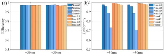
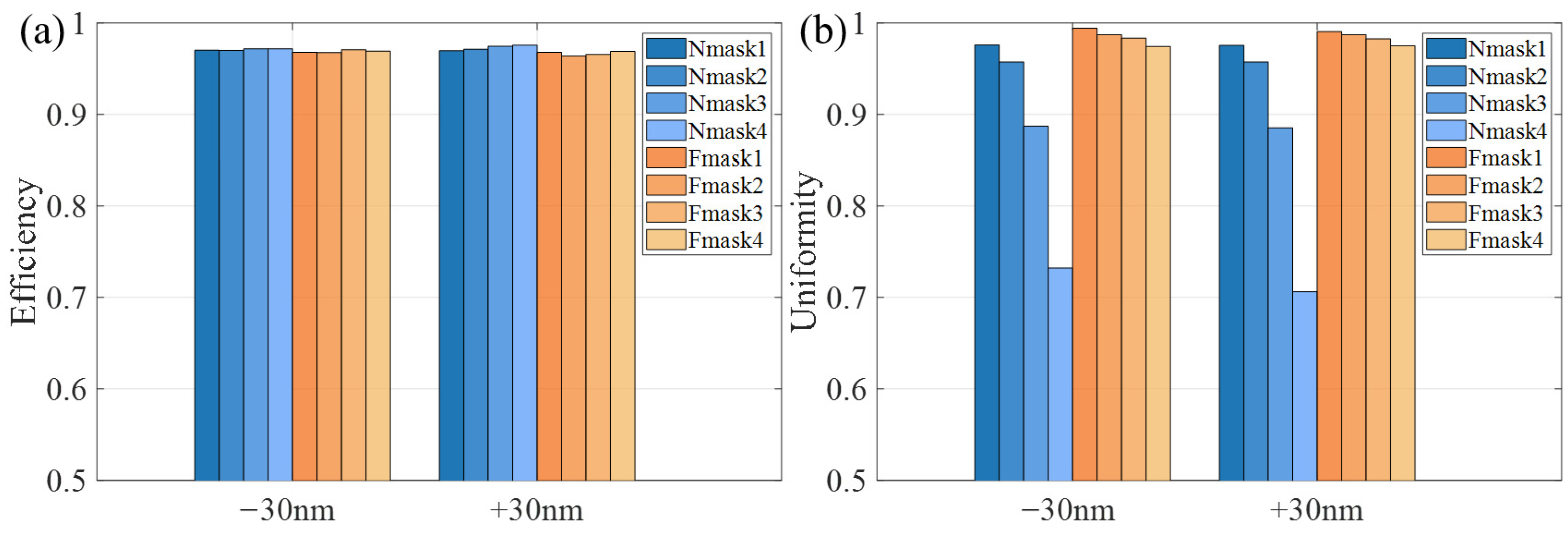
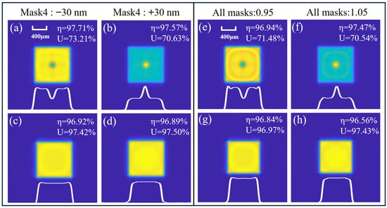
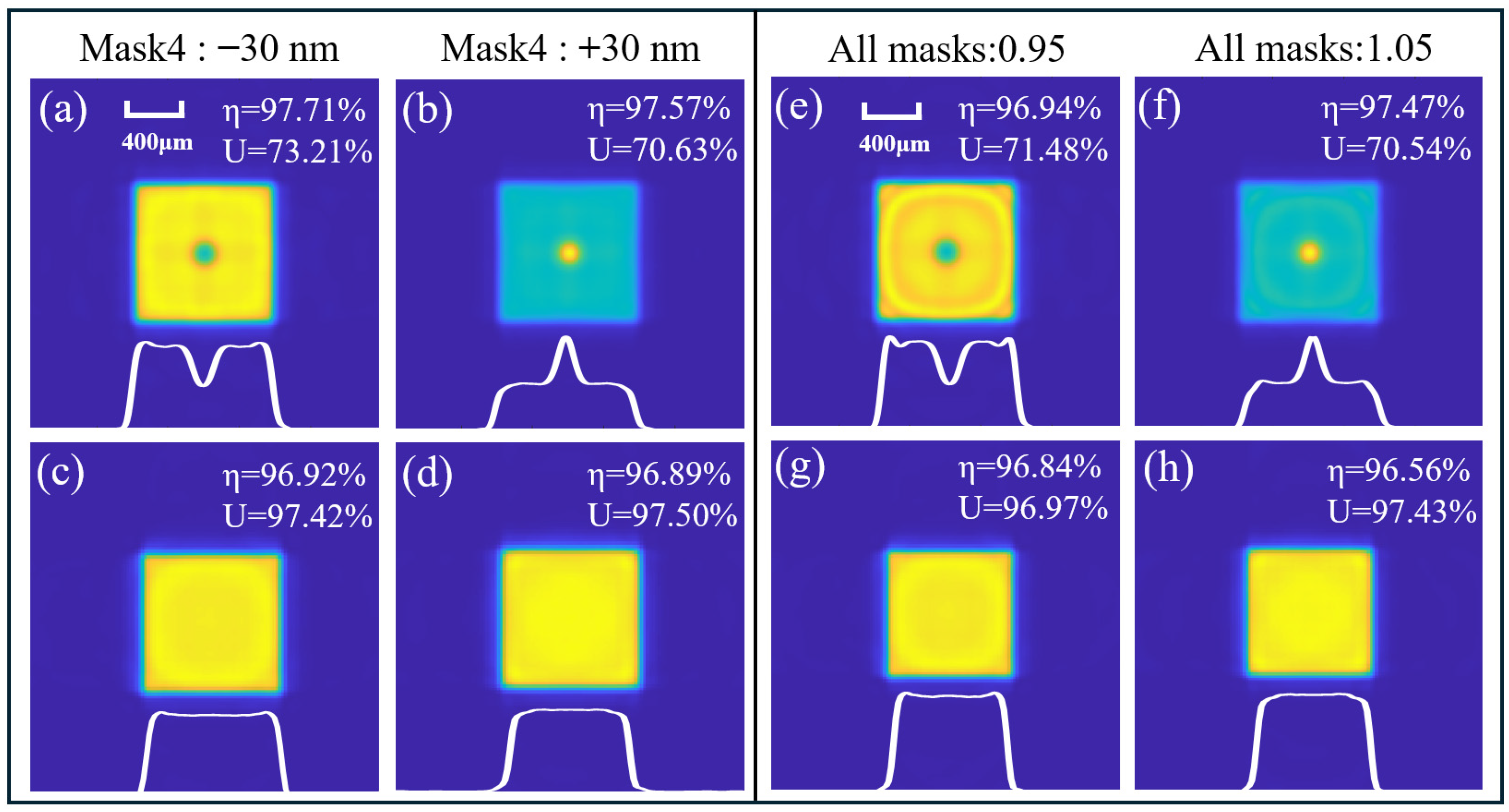
Next, we introduce the same etching depth error into the non-focusing DOEs and the focusing DOEs and compare the beam shaping quality. According to the simulation parameters set in this work, the four masks of the 16-step DOEs are mask1, mask2, mask3, and mask4, and their corresponding theoretical etching depths are 72.17 nm, 144.35 nm, 288.69 nm, and 1082.59 nm, respectively. The simulation results when a single mask of the 16-step DOEs has an etching depth error of ±30 nm are shown in Figure 4a,b. It can be observed that with an etching depth error of ±30 nm, the non-focusing DOEs maintain a high efficiency of more than 96%, but the uniformity corresponding to mask1, mask2, mask3, and mask4 gradually decreases, with a minimum uniformity of only 70.63%. In contrast, the focusing DOEs not only maintain a high efficiency of more than 96%, but also achieve a uniformity above 97% under the same error condition. However, it can also be observed that the uniformity corresponding to mask1, mask2, mask3, and mask4 of the focusing DOEs also exhibits a gradually decreasing trend. This indicates that the etching depth errors exert a greater influence on the masks with larger theoretical etching depths because the 16-step phase is superimposed by mask1 to mask4 with different weights. The larger the etching depth corresponding to a mask, the higher its weight in phase superposition will be. Even a small depth error can cause the uniformity of a large number of phase steps to be disrupted. Therefore, the etching depth error occurring in mask4 has the most significant negative impact, thus resulting in the worst beam shaping performance, as shown in Figure 5a–d.
Figure 4.
The simulated performance comparison of (a) diffraction efficiency and (b) uniformity between non-focusing DOEs (Nmask1–4) and focusing DOEs (Fmask1–4) at etching depth errors of −30 nm and +30 nm.
Figure 5.
The simulated intensity distributions of square flat-top beams: (a) mask4 of non-focusing DOE at −30 nm etching depth error, (b) mask4 of non-focusing DOE at +30 nm etching depth error, (c) mask4 of focusing DOE at −30 nm etching depth error, (d) mask4 of focusing DOE at +30 nm etching depth error, (e) non-focusing DOE with all masks at an etching depth error ratio of 0.95, (f) non-focusing DOE with all masks at an etching depth error ratio of 1.05, (g) focusing DOE with all masks at an etching depth error ratio of 0.95, (h) focusing DOE with all masks at an etching depth error ratio of 1.05.
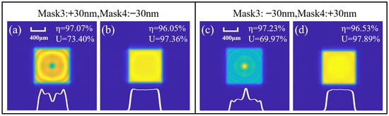
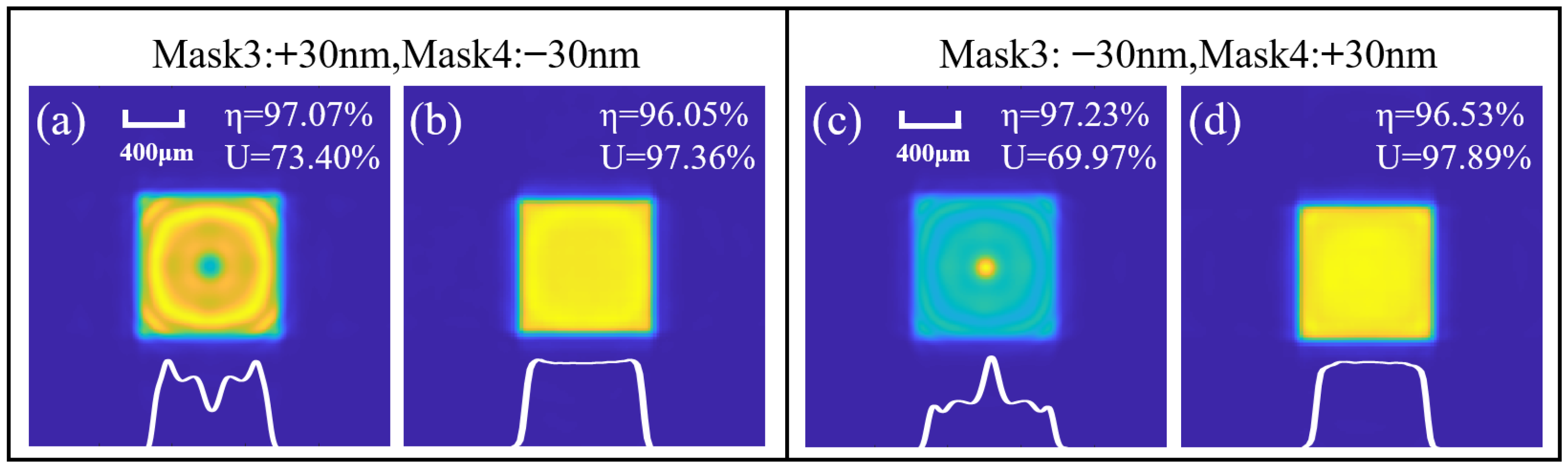
In addition to the etching depth error occurring on a single mask of the 16-step DOEs, simulations were also performed when all four masks had the same etching depth error ratio, with the scaling factors set to 0.95 and 1.05. The simulation results are shown in Figure 5e–h. It can be seen that the non-focusing DOEs maintain a high efficiency of over 96%, but their uniformity is only about 70%. In contrast, the focusing DOEs achieve high uniformity of 96.97% and 97.43% respectively while retaining high efficiency. Next, we consider the scenario of combined errors occurring in the 16-step DOEs. Given that mask3 and mask4 have higher weights and larger etching depths, we only introduce such combined errors in these two masks, with the etching depth errors set to ±30 nm. The simulation results are shown in Figure 6. It can be observed that the non-focusing DOEs still exhibit poor uniformity under such combined errors. In contrast, the focusing DOEs maintain an efficiency of approximately 96% and a uniformity of around 97%, respectively. Therefore, the simulation results demonstrate that the proposed focusing DOEs can effectively resist the adverse effects caused by various etching depth errors.
Figure 6.
The simulated intensity distributions of square flat-top beams: (a) non-focusing DOE with mask3 at +30 nm and mask4 at −30 nm etching depth errors, (b) focusing DOE with mask3 at +30 nm and mask4 at −30 nm etching depth errors, (c) non-focusing DOE with mask3 at −30 nm and mask4 at +30 nm etching depth errors, (d) focusing DOE with mask3 at −30 nm and mask4 at +30 nm etching depth errors.
4. Experiment
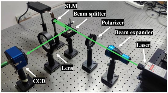
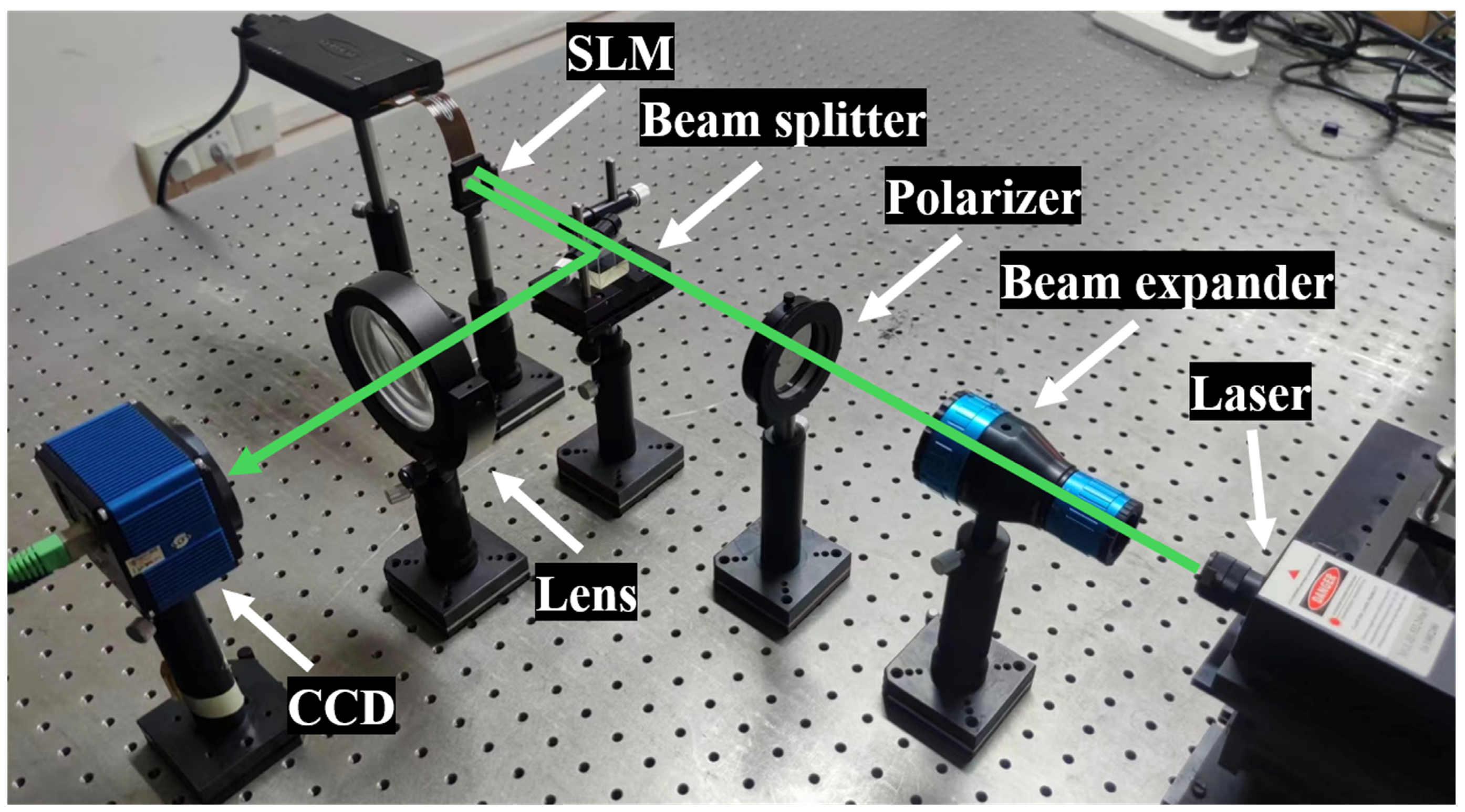
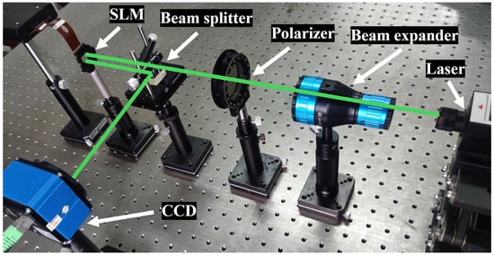
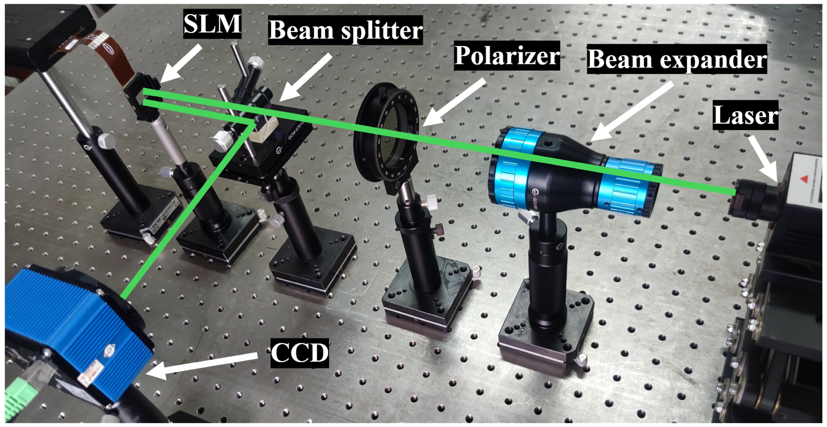
To further validate the feasibility of the proposed approach in suppressing etching depth error effects, optical experiments were performed. The configuration of the optical experimental setup is shown in Figure 7 and Figure 8. A near-Gaussian (TEM00) laser beam with a wavelength of 532 nm was used as the input beam. And a beam expander was adopted to adjust its waist radius to 1.6 mm. A Holoeye PLUTO SLM (Holoeye Photonics AG, Berlin, Germany) was employed, featuring a high resolution of 1920 × 1080 pixels and a pixel size of 8 μm. The input grayscale signal of the phase-only SLM ranges from 0 to 255 (8-bit). The corresponding modulated phase spans from 0 to 2π, and the maximum phase depth of the SLM is 2π. Since etching depth regulates diffraction by introducing phase differences of light, the grayscale values of the quantized phase distribution with etching depth errors are linearly mapped to the phase range of 0 to 2π. To avoid the influence of the zero-order diffraction of SLM, all phase-only distributions are multiplied by phase grating. The reconstructed flat-top beams are reflected from the beam splitter and captured at a propagation distance of 300 mm after modulation. The resolution of the HR16000CTLGEC camera (SVS-Vistek GmbH, Seefeld, Germany) is 4896 × 3248 with pixel size of 7.4 μm.
Figure 7.
Schematic of optical experimental setup with Fourier lens.
Figure 8.
Schematic of optical experimental setup without Fourier lens.
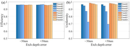
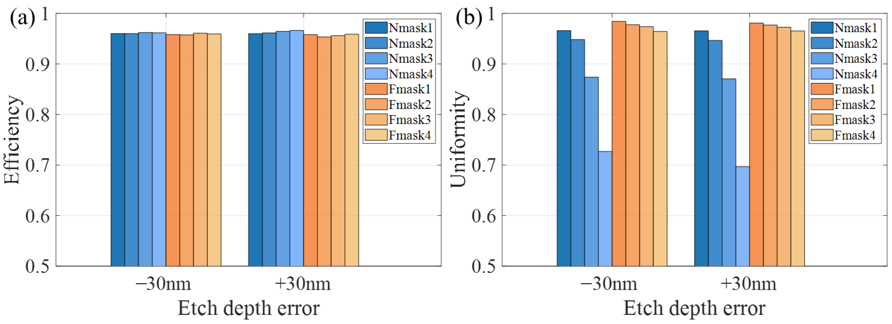
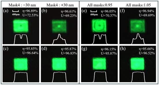
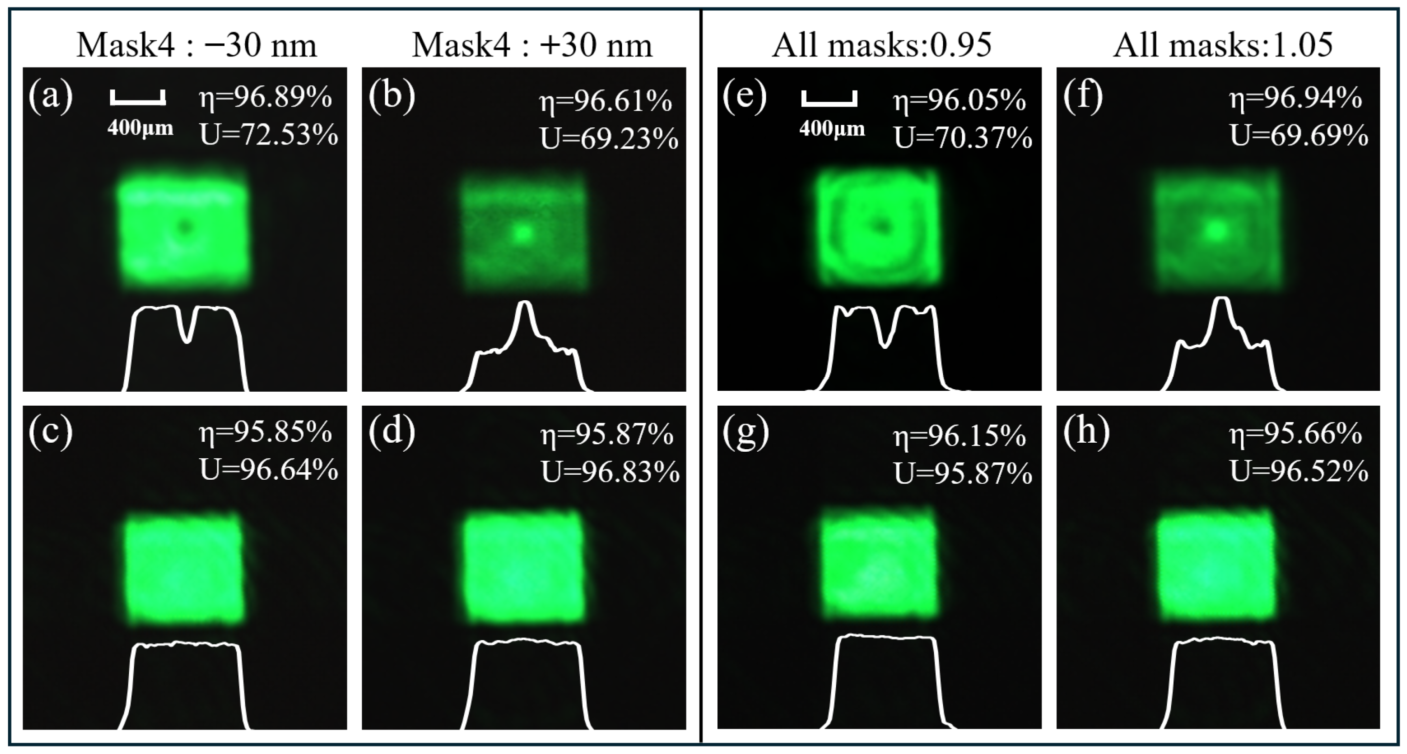
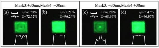
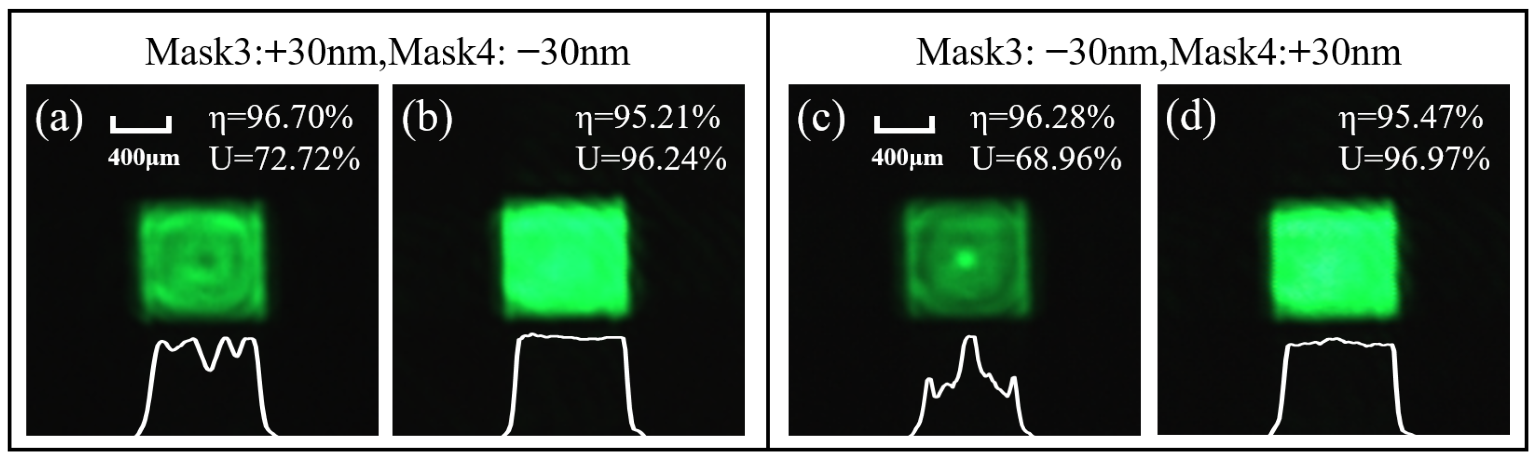
The experimental results when a single mask of the 16-step DOEs has an etching depth error of ±30 nm are shown in Figure 9a,b. The efficiency of the non-focusing DOEs decreases slightly with the increase in theoretical etching depth of the masks, but remains above 95%, while the uniformity drops sharply with the increase in theoretical etching depth, reaching a minimum of only 69.23%. In contrast, both the efficiency and uniformity of the focusing DOEs can be maintained above 95%. The negative impact of the etching depth error is most pronounced for mask4, which exhibits the worst beam shaping performance. Figure 10a–d show the square flat-top beams obtained when etching errors occur in mask4. Similar to the results under a ±30 nm etching depth error in mask4, when all four masks have the same etching depth error ratio, the non-focusing DOEs can maintain high efficiency but their uniformity drops to a minimum of only 69.69%. On the contrary, both the efficiency and uniformity of the focusing DOEs remain above 96%, as shown in Figure 10e–h. The experimental results under the combined errors are shown in Figure 11a–d. Both the efficiency and uniformity of the non-focusing DOEs are lower than those of the focusing DOEs, especially the uniformity, which is only about 70%. There is a slight difference between the experimental results and the simulation results. The minor difference is mainly attributed to the deviation of the incident beam profile from the ideal Gaussian model and the inaccurate optical alignment. However, the trend of uniformity and energy utilization of the flat-top beams is very consistent with the simulation results. These experimental results further prove that the focusing DOEs we proposed can effectively resist etching depth errors.
Figure 9.
The experimental performance comparison of (a) diffraction efficiency and (b) uniformity between non-focusing DOEs (Nmask1–4) and focusing DOEs (Fmask1–4) at etching depth errors of −30 nm and +30 nm.
Figure 10.
The experimentally measured intensity distributions of square flat-top beams: (a) mask4 of non-focusing DOE at −30 nm etching depth error, (b) mask4 of non-focusing DOE at +30 nm etching depth error, (c) mask4 of focusing DOE at −30 nm etching depth error, (d) mask4 of focusing DOE at +30 nm etching depth error, (e) non-focusing DOE with all masks at an etching depth error ratio of 0.95, (f) non-focusing DOE with all masks at an etching depth error ratio of 1.05, (g) focusing DOE with all masks at an etching depth error ratio of 0.95, (h) focusing DOE with all masks at an etching depth error ratio of 1.05.
Figure 11.
The experimentally measured intensity distributions of square flat-top beams: (a) non-focusing DOE with mask3 at +30 nm and mask4 at −30 nm etching depth errors, (b) focusing DOE with mask3 at +30 nm and mask4 at −30 nm etching depth errors, (c) non-focusing DOE with mask3 at −30 nm and mask4 at +30 nm etching depth errors, (d) focusing DOE with mask3 at −30 nm and mask4 at +30 nm etching depth errors.
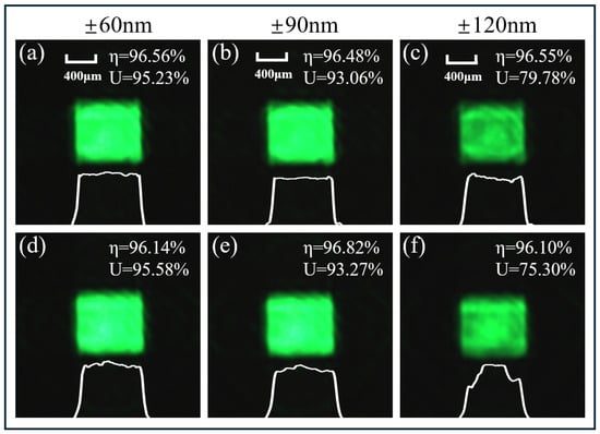
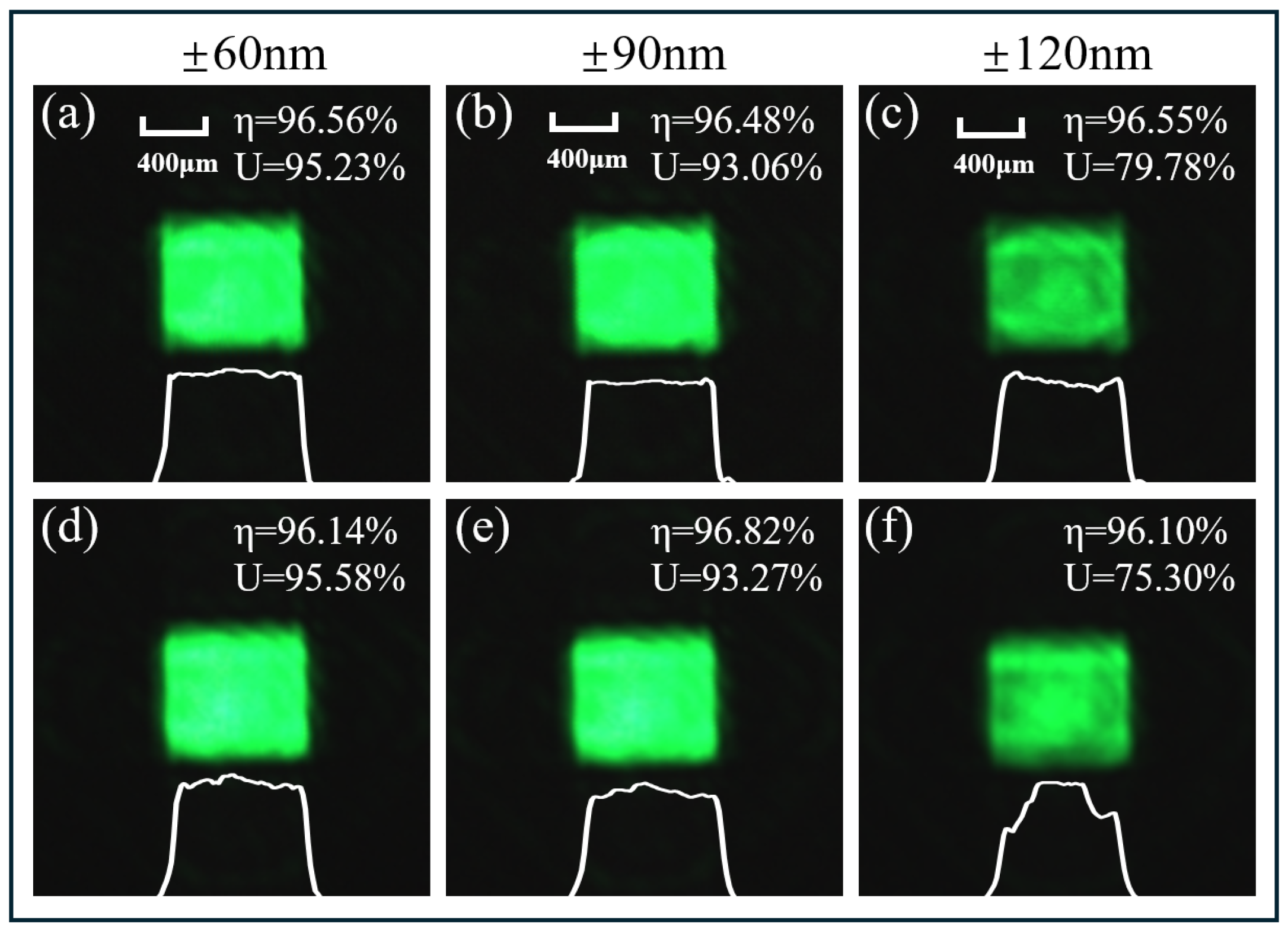
Previously, we have verified through numerical simulation and experiments that the focusing DOEs can effectively resist the influence of etching depth errors. Next, we discuss the maximum tolerable etching depth error of the focusing DOEs. We already know that etching depth errors occurring on mask4 impose a stronger adverse impact on the final output optical field compared with etching depth errors on mask1, mask2, and mask3. Therefore, we only need to focus on the discussion of mask4. The etching depth error was set at ±60 nm, ±90 nm, and ±120 nm. Other experimental parameters remained the same as before. The experimental results in Figure 12a–f show that the flat-top beam maintains a high efficiency of approximately 96% as the etching depth error increases, whereas the uniformity gradually deteriorates. When the etching depth error reaches ±120 nm, the uniformity of the resulting square flat-top beam drops to no more than 79.78%. Accordingly, we can conclude that the focusing DOE can tolerate a maximum etching depth error of ±90 nm. Under this error level, the efficiency and uniformity of the square flat-top beam can be maintained at approximately 96% and 93%, respectively.
Figure 12.
The experimentally measured intensity distributions of square flat-top beams: (a) mask4 of the focusing DOE at −60 nm etching depth error, (b) mask4 of the focusing DOE at −90 nm etching depth error, (c) mask4 of the focusing DOE at −120 nm etching depth error, (d) mask4 of the focusing DOE at +60 nm etching depth error, (e) mask4 of the focusing DOE at +90 nm etching depth error, (f) mask4 of the focusing DOE at +120 nm etching depth error.
5. Discussion
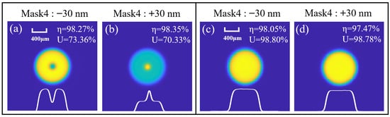
For focusing DOEs, target geometry has no impact on their capability to resist etching depth errors, and excellent error robustness can be achieved for different beam shapes. Supplementary simulations of circular flat-top beams are implemented for verification. We analyze the scenario where mask4 of the 16-step DOE introduces ±30 nm etching depth error, and the simulated results are shown in Figure 13. The simulation results indicate that under ±30 nm etching depth error, the focusing DOE keeps both efficiency and uniformity above 97%. In contrast, although the non-focusing DOE still maintains high diffraction efficiency, its uniformity declines sharply, reaching a minimum of only 70.33%.
Figure 13.
Intensity distributions of circular flat-top beams: (a) non-focusing DOE with mask4 at −30 nm etching depth errors, (b) non-focusing DOE with mask4 at +30 nm etching depth errors, (c) focusing DOE with mask4 at −30 nm etching depth errors, (d) focusing DOE with mask4 at +30 nm etching depth errors.
In addition, the method presented in this paper is not limited to 16-step phase structures and can also be applied to 8-step and 32-step diffractive optical elements. The number of phase quantization levels primarily determines the initial shaping quality under ideal conditions without fabrication errors, while the core characteristic of integrated focusing phase suppressing stray light convergence remains valid across different quantization levels.
6. Conclusions
In conclusion, we propose a focusing DOE for flat-top beam shaping with strong robustness against etching depth errors. The scheme combines the focusing phase and the phase optimized via a weighted constrained iterative algorithm to realize flat-top beam shaping. Within ±30 nm etching depth error, the designed DOE can reliably transform incident Gaussian beams into flat-top beams, achieving experimental uniformity and diffraction efficiency higher than 95%. Furthermore, the target flat-top geometry and phase quantization levels impose no influence on its error suppression performance, and the maximum tolerable etching depth error reaches ±90 nm. Benefiting from the integrated focusing function, this DOE removes the requirement for an additional focusing lens, simplifying the optical setup and enhancing system stability. This design is promising for integrated DOE development and high-precision optical applications.
Author Contributions
Conceptualization, X.Z. and H.P.; methodology, X.Z.; software, X.Z.; validation, X.Z., H.P. and C.X.; investigation, X.Z.; resources, A.C.; writing—original draft preparation, X.Z.; writing—review and editing, H.P.; supervision, Q.D. and Y.F.; funding acquisition, H.P. All authors have read and agreed to the published version of the manuscript.
Funding
This research received no external funding.
Institutional Review Board Statement
Not applicable.
Informed Consent Statement
Not applicable.
Data Availability Statement
The data underlying the results presented in this paper are not publicly available at this time but may be obtained from the authors upon reasonable request.
Conflicts of Interest
The authors declare no conflicts of interest.
References
- Caprio, L.; Previtali, B.; Demir, A.G. Effect of in-source beam shaping and laser beam oscillation on the electromechanical properties of Ni-plated steel joints for e-vehicle battery manufacturing. J. Laser Appl. 2023, 35, 042030. [Google Scholar] [CrossRef] [Scilit]
- Jun, H.U.; Kim, J.D.; Cheon, J.; Kim, J.; Park, Y.D.; Kim, Y.D.; Ji, C. Microstructure and mechanical properties of adjustable-ring-mode laser welded and hot-stamped Al-Si coated boron steel joints. J. Mater. Res. Technol. 2024, 28, 844–855. [Google Scholar] [CrossRef] [Scilit]
- Li, J.; Zhao, R.; Bi, J. Particle metrology and classification instrumentation based on dual-wavelength illumination and modulated polarization detection. IEEE Trans. Instrum. Meas. 2024, 73, 1–11. [Google Scholar] [CrossRef] [Scilit]
- Khonina, S.N.; Kazanskiy, N.L.; Skidanov, R.V.; Butt, M.A. Advancements and applications of diffractive optical elements in contemporary optics: A comprehensive overview. Adv. Mater. Technol. 2025, 10, 240102. [Google Scholar] [CrossRef] [Scilit]
- Laskin, A.; Laskin, V.; Ostrun, A. Beam shaping for holographic techniques. Proc. SPIE 2014, 9200, 92000E. [Google Scholar] [CrossRef] [Scilit]
- Yan, V.T.; Voznesenskaya, A.O. Modeling of a focal pi-Shaper using the ray-mapping method. J. Opt. Technol. 2023, 90, 242–248. [Google Scholar] [CrossRef] [Scilit]
- Sheldakova, J.; Galaktionov, I.; Nikitin, A.; Rukosuev, A.; Kudryashov, A. LC phase modulator vs. deformable mirror for laser beam shaping: What is better? Proc. SPIE 2018, 10744, 107440S. [Google Scholar]
- Ding, H. Optimization algorithm for flattop beam shaping using analytically initial phase. IEEE Photonics Technol. Lett. 2024, 36, 1285–1288. [Google Scholar] [CrossRef] [Scilit]
- Ma, H.; Liu, Z.; Jiang, P.; Xu, X.; Du, S. Improvement of Galilean refractive beam shaping system for accurately generating near-diffraction-limited flattop beam with arbitrary beam size. Opt. Express 2011, 19, 13105–13117. [Google Scholar] [CrossRef] [Scilit] [PubMed]
- Bi, J.; Engarnevis, A.; Zhang, J.; Zhang, M.; Li, J. Flat-top beam shaping and optimization based on a single aspheric lens. Opt. Laser Technol. 2025, 183, 112391. [Google Scholar] [CrossRef] [Scilit]
- Chen, Z.; Ning, X.; Chen, J.; Hua, J.; Lu, W. Beam shaping based on axisymmetric aspheric mirrors. Opt. Commun. 2025, 581, 131656. [Google Scholar] [CrossRef] [Scilit]
- Wang, D. Color liquid crystal grating based color holographic 3D display system with large viewing angle. Light Sci. Appl. 2024, 13, 16. [Google Scholar] [CrossRef] [Scilit] [PubMed]
- Liu, S.; Feng, L.; Ji, S.; Yan, H.; Yang, K.; Li, P.; Wang, D. Speckle noise suppression method in holographic display using optimized pixel processing. Opt. Laser Technol. 2025, 181, 111644. [Google Scholar] [CrossRef] [Scilit]
- Barlev, O.; Golub, M. Multifunctional binary diffractive optical elements for structured light projectors. Opt. Express 2018, 26, 21092–21107. [Google Scholar] [CrossRef] [Scilit] [PubMed]
- Yoneda, N.; Saita, Y.; Nomura, T. Motionless optical scanning holography. Opt. Lett. 2020, 45, 3184–3187. [Google Scholar] [CrossRef] [Scilit] [PubMed]
- Chen, W.; Mao, J.; Chen, K.; Li, X.; Tan, Y.; Li, M.; Zhang, L. Generation of high uniformity flat-top beams by reconstructing the amplitude distribution at descending edges. Opt. Laser Technol. 2025, 186, 112776. [Google Scholar] [CrossRef] [Scilit]
- Li, K.; Gui, J.; Li, M.; Liu, H.; Zhong, W. Optimized iterative algorithm for generating phase-only Fourier hologram based on phase momentum. Opt. Commun. 2026, 606, 132860. [Google Scholar] [CrossRef] [Scilit]
- Chen, W.; Mao, J.; Chen, K.; Li, X.; Tan, Y.; Li, M.; Zhang, L. Lensless beam shaping for zero-order-free flat-top beams in femtosecond laser processing. Opt. Laser Technol. 2026, 194, 114527. [Google Scholar] [CrossRef] [Scilit]
- Fuse, K. Beam shaping for advanced laser materials processing. Laser Tech J. 2015, 12, 19–22. [Google Scholar] [CrossRef] [Scilit]
- Suresh, S.A.; Vyas, S.; Yeh, J.A.; Luo, Y. Characterization of super-Gaussian beams generated through volume holography. Opt. Laser Technol. 2025, 190, 113237. [Google Scholar] [CrossRef] [Scilit]
- Kazanskiy, N.L.; Uspleniev, G.V.; Volkov, A.V. Fabricating and testing diffractive optical elements focusing into a ring and into a twin-spot. Proc. SPIE 2000, 4316, 193–199. [Google Scholar] [CrossRef] [Scilit]
- Golub, M.A. New diffractive beam shaper generated with the aid of e-beam lithography. Opt. Eng. 1996, 35, 1400–1406. [Google Scholar] [CrossRef] [Scilit]
- Luan, H.; Xing, Y.; Bai, Y.; Dong, Y.; Gu, M. Laser-nanoprinting-enabled multilevel nanoscale phase encoding on quartz for integrated optical diffractive devices. Light Adv. Manuf. 2026, 7, 31. [Google Scholar] [CrossRef] [Scilit]
- Cunha, J.; Garcia, I.S.; Santos, J.D.; Fernandes, J.; González-Losada, P.; Silva, C.; Gaspar, J.; Cortez, A.; Sampaio, M.; Aguiam, D.E. Assessing tolerances in direct write laser grayscale lithography and reactive ion etching pattern transfer for fabrication of 2.5D Si master molds. Micro Nano Eng. 2023, 19, 100182. [Google Scholar] [CrossRef] [Scilit]
- Niu, B. A PDMS-Polymer Based Flexible DOE for Tunable Beam Shaping. J. Light. Technol. 2026, 44, 634–643. [Google Scholar] [CrossRef] [Scilit]
- You, R. Extremely Compact 3D Printed Glass Ternary Diffractive Optical Element for Holographic Images. Adv. Opt. Mater. 2025, 13, 2501074. [Google Scholar] [CrossRef] [Scilit] [PubMed]
- Chen, Y.; Pu, S.; Hou, M.; Li, L.; Liu, S.; Li, D.; Yi, F. Lightweight and efficient beam-shaping metalens for converting Gaussian beams into 2D flat-top beams. Opt. Express 2025, 33, 11555–11573. [Google Scholar] [CrossRef] [Scilit] [PubMed]
- Chen, L.; Zhang, H.; He, Z.; Wang, X.; Cao, L.; Jin, G. Weighted Constraint Iterative Algorithm for Phase Hologram Generation. Appl. Sci. 2020, 10, 3652. [Google Scholar] [CrossRef] [Scilit]
- Liu, J.S.; Thomson, M.J.; Taghizadeh, M.R. Automatic symmetrical iterative Fourier-transform algorithm for the design of diffractive optical elements for highly precise laser beam shaping. J. Mod. Opt. 2006, 53, 461–471. [Google Scholar] [CrossRef] [Scilit]
- Hsu, K.H.; Lin, H.Y. Design of diffractive beam shaper for transforming a Gaussian beam to a squared uniform beam. Proc. SPIE 2008, 6832, 68320U. [Google Scholar] [CrossRef] [Scilit]
- Pang, H.; Liu, W.; Cao, A.; Deng, Q. Speckle-reduced holographic beam shaping with modified Gerchberg-Saxton algorithm. Opt. Commun. 2019, 433, 44–51. [Google Scholar] [CrossRef] [Scilit]
Disclaimer/Publisher’s Note: The statements, opinions and data contained in all publications are solely those of the individual author(s) and contributor(s) and not of MDPI and/or the editor(s). MDPI and/or the editor(s) disclaim responsibility for any injury to people or property resulting from any ideas, methods, instructions or products referred to in the content. |
© 2026 by the authors. Licensee MDPI, Basel, Switzerland. This article is an open access article distributed under the terms and conditions of the Creative Commons Attribution (CC BY) license.