


Abstract
This work presents a laboratory prototype of an Electron-Bombarded Active Pixel Sensor (EBAPS) to investigate the effects of passivation film thickness on electron energy loss and bombardment gain. Through combined experimental characterization and numerical simulations, we systematically examine the correlations among accelerating voltage, passivation layer thickness, electron gain, and dead-layer energy dissipation. Experimental results show that the fabricated EBAPS achieves a spatial resolution of 18 lp/mm at an accelerating voltage of 8000 V. Reducing the passivation layer thickness from 70 nm to 30 nm decreases dead-layer energy loss from 2000 eV to 1000 eV. An optimized Monte Carlo model is developed to simulate electron penetration behaviors under different thicknesses and voltages, and its predictions are in good agreement with experimental data. This study confirms that thinning the passivation layer effectively lowers the required bombardment voltage and improves the long-term operational reliability of EBAPS devices. These findings offer both experimental evidence and theoretical guidance for substrate thinning and surface modification strategies in EBAPS development.
1. Introduction
Low-light level imaging and weak spectrum studies in astronomy, cosmology, planetary studies, biology, medical applications, and in many other cases often require night vision technology or photon-counting detection. Many night vision imaging devices exist and can be classified as vacuum electron tube detectors or solid-state detectors according to their fabrication process.
Many kinds of vacuum electron tubes have been developed; for example, image intensifiers, Photomultiplier Tubes (PMTs), Intensified Charge Coupled Devices (ICCDs) [1], Electron-Bombarded CCDs (EBCCDs) [2,3,4], and single-photon anode detectors [5,6], among others. Typically, they convert low levels of light photons into electrons using a photocathode, amplify the resulting electrons using dynodes or a microchannel plate, and then convert the electrons back into photons of light or output an electronic pulse signal. Vacuum electron tube detectors usually have high sensitivity (<10−6 lx), a fast response time (<ns) and precise shutter control. Many instruments based on vacuum electron tube detectors have been developed, such as the JUNO space probe [7], the IMAGE Spectrographic Imager (SI) [8], the ICON Far Ultra Violet Imaging Spectrograph (ICON FUV) instrument [9], and the SOHO Solar and Heliospheric Observatory [10]. These spaceborne instruments have been used to identify the compositions of asteroids and planetary atmospheres, observe weather patterns, solar winds, and auroras, categorize solar flares, and discover distant planets, gamma-ray bursts, black holes, and galaxies. They have been widely used in space applications. Vacuum tube detectors are generally complex in structure and have the disadvantages of large size, high voltage, high cost, and poor stability. These shortcomings make them difficult to adapt for common commercial applications.
Solid-state detectors are photosensitive devices that convert light signals into digital signals. The main types used for night vision imaging are Charge-Coupled Devices (CCDs), Electron-Multiplying CCDs (EMCCDs) [11], and complementary metal-oxide semiconductors (CMOS). These use photodiodes to capture light and convert it to digital data. They have the advantages of small volume, light weight, low power consumption and high reliability. The detection sensitivity of solid-state detectors is 10−3 lx, which is far worse than electric vacuum devices.
Electron Bombarded Active Pixel Sensors (EBAPSs, also called EBCMOS) [12,13] are hybrid detectors that combine the advantages of electric vacuum devices and solid-state detectors. Firstly, EBAPSs have a lower dark noise than vacuum tubes and EMCCDs. The excess noise factor of vacuum tubes with MCPs and EMCCDs is 1.8 and 1.4, respectively [14]. The gain in an EBAPS is produced through electron bombardment of the semiconductors. This gain process inherently exhibits a low excess noise factor of less than 1.1. Due to its electron bombardment gain, the sensitivity of an EBAPS is higher than that of CMOS, making it widely applicable for low-light detection. Secondly, an EBAPS has a smaller volume, lower power consumption, and better reliability than an image intensifier. In image intensifiers, the anode typically consists of an optical fiber phosphor screen, which is the heaviest component in the device. Using a CMOS as the anode is lighter than an optical fiber panel. Thirdly, the EBAPS has better image quality than ICCDs. To obtain an image from the image intensifier, the phosphor screen must be coupled with a CMOS or CCD using a fiber taper. The use of an optical fiber taper will not only significantly increase the weight of the detector, but also create two coupling surfaces. The existence of coupling surfaces will reduce the sensitivity and resolution of the detector. The EBAPS can directly output the captured image through CMOS. Without fiber taper coupling, the EBAPS has a lower weight and better image quality.
Although the EBAPS offers lower dark noise and higher sensitivity, high-energy electrons bombarding the APS rapidly decelerate in the Si material, and the resulting loss in kinetic energy generates bremsstrahlung X-rays. Prolonged exposure to these X-rays damages the Si lattice structure, resulting in increased dark current. Moreover, excessively high electron energies can also generate positive ions inside the vacuum cavity during bombardment. Driven by the cathode’s negative voltage, these ions travel toward the photocathode, causing ion feedback that degrades both the performance and the operational lifetime of the photocathode. Therefore, reducing the electron bombardment voltage is an effective way to improve the long-term performance of the EBAPS. Substrate thinning and passivation layer thinning are widely adopted as mainstream methods to reduce the required bombardment voltage.
In this study, we built an EBAPS verification system in the laboratory and studied the relationship between electron bombardment gain and accelerating voltage. The electron bombardment gain curve, voltage consumed by the dead layer, resolution, and other performance metrics of EBAPSs with different passivation film thicknesses were studied.
2. Methods
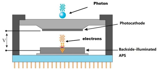
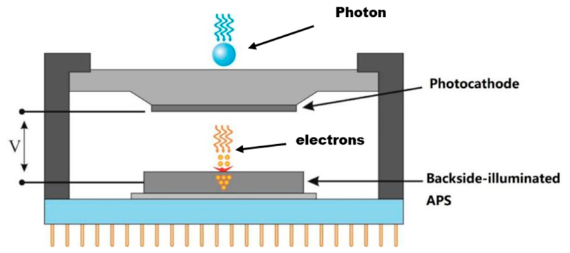
As shown in Figure 1, EBAPSs are mainly composed of a photocathode and back-illuminated APS. In this study, we used a back-illuminated CMOS as the back-illuminated APS. Incident light is absorbed by the photocathode, which emits photoelectrons. Under a high negative voltage, these photoelectrons are accelerated by several keV before bombarding the back-illuminated APS. The accelerated electrons bombard the Si substrate, generating charge carriers via energy deposition and inducing secondary electron multiplication. The multiplied electrons are read out by the CMOS chip to form electron bombardment images.
Figure 1.
Diagram of the EBAPS.
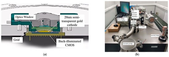
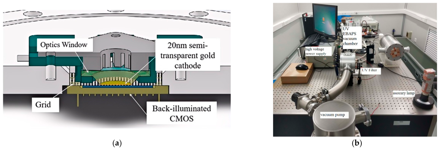
To study the relationship between the EBAPS gain curve and the passivation layer thickness, a demonstration system was built in the laboratory. The system mainly includes an ultraviolet light source (mercury lamp), a photocathode, a CMOS, image acquisition electronics, and a high-voltage power supply. As shown in Figure 2a, a semi-transparent 20 nm thick gold cathode was deposited on a quartz optical window via electron beam evaporation. The gold cathode provides stable photoelectric conversion efficiency to convert ultraviolet photons into electrons. The high-voltage power supply ranges from 0 to 10 kV with continuous adjustability. A commercial scientific-grade back-illuminated GSENSE400BSI CMOS (APS) chip purchased from Gpixel Inc. (Changchun, China) had a 2048 (H) × 2048 (V) resolution and response range of 200–1100 nm. The CMOS sensor operated at a room temperature of (25 °C). The camera gain was set to 0, and the exposure time was 100 ms. The EBAPS demo system was placed in a vacuum chamber and evacuated to 10−4 Pa.
Figure 2.
EBAPS demonstration system schematic diagram and physical diagram. (a) System schematic diagram; (b) Physical photograph of the experimental setup.
3. Results and Discussion
3.1. Experimental Setup Improvement
In the actual experiment, as the negative voltage applied to the cathode window increased, the Digital Number (DN) value of the output image did not change significantly. This is likely due to the low quantum efficiency of the gold cathode, which is only about 10−6 [15,16]. In contrast, the average quantum efficiency of the CMOS sensor is above 50%, which is much higher than that of the gold cathode. Even if the electron bombardment gain reaches more than 2000, the equivalent quantum efficiency of the gold cathode is 2 × 10⁻³, which is still far lower than that of the CMOS sensor. This also results in the electron bombardment images’ DN value being much lower than that of directly detected photon images. To clearly observe the electron bombardment signal, the following improvements are proposed:
Firstly, a photocathode with higher quantum efficiency can be used. If the quantum efficiency of the photocathode is 1%, considering the electron bombardment gain, the equivalent quantum efficiency is more than 100 times higher than that of CMOS, making the electron bombardment image easier to distinguish from the optical image. High-quantum-efficiency photocathodes such as multialkali photocathodes and bialkali photocathodes require an ultrahigh vacuum (10−6 pa~10−7 pa), which cannot be achieved by a conventional vacuum system.
Secondly, the visible light image and the electron bombardment image are spatially separated.
Thirdly, the proportion of visible light in the mercury lamp is reduced. According to the mercury emission spectrum, the energy of a mercury lamp is mainly concentrated in the visible light band. For CMOS sensors, the sensitivity to visible light is several times higher than that to ultraviolet light, and visible light has no beneficial effect on increasing the photocathode optoelectronics output. By placing a 254 nm (half-height width 10 nm) narrow-band filter between the mercury lamp and the light window, ineffective visible light can be filtered out, and the DN value of the visible light image can be reduced. This increases the intensity ratio of the electron bombardment image to the visible light image, thereby making the electron bombardment image easier to distinguish from the visible image. After adding the 254 nm filter, the light intensity at the cathode window is 2 μW/cm2.
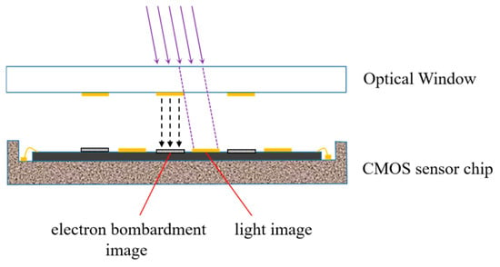
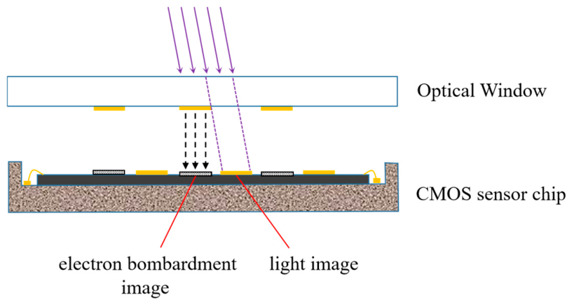
At 254 nm, the quantum efficiency of the CMOS detector is 30%, which is 105 times greater than the quantum efficiency of the gold cathode at 254 nm. Even when considering an electron bombardment gain of several thousand, the intensity of the electron bombardment image is nearly a hundred times lower than that of the optical image, meaning that the electron bombardment image still cannot be clearly observed. To more clearly distinguish the electron bombardment image from the optical image, the ultraviolet light is positioned to be obliquely incident to spatially separate the optical image and the electron bombardment image. The principle is shown in Figure 3.
Figure 3.
Schematic diagram of the spatial separation of an electron bombardment image and a light image.
3.2. Gain Characteristics of Electron Bombardment
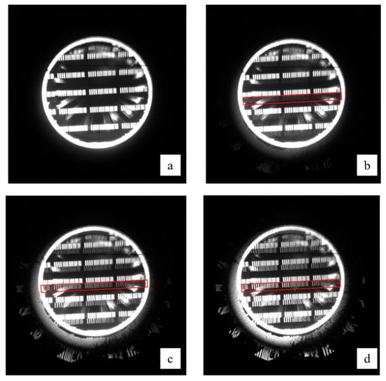
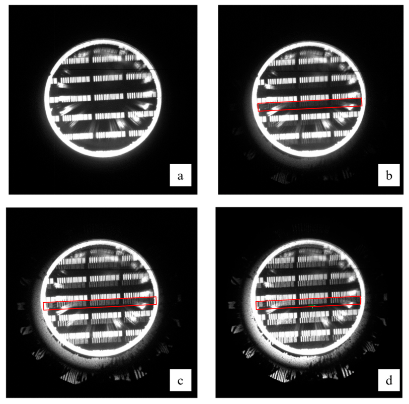
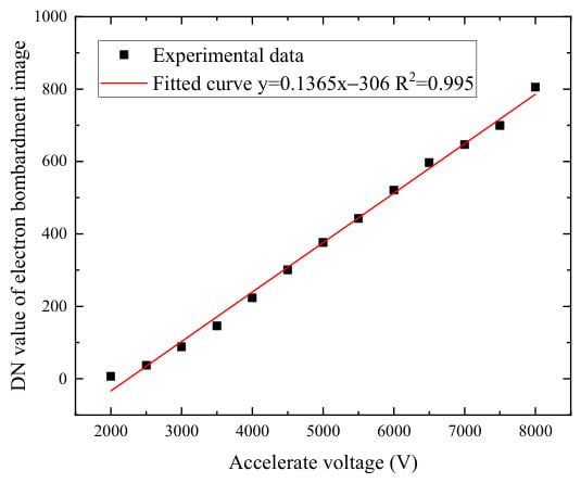
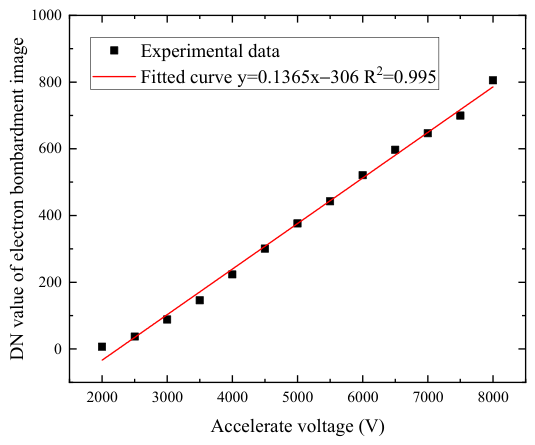
After background and dark corrections, Figure 4 shows an optical image and an electron bombardment image obtained under different acceleration voltages. Figure 5 presents a statistical table of the data obtained by gradually adjusting the voltage from 2000 V to 8000 V. It can be clearly seen in Figure 4 and Figure 5 that the DN value of the electron bombardment image increases with the acceleration voltage. The electron bombardment gain can be expressed in the following formula:
Figure 4.
Electron bombardment images and light images at different voltages (the areas in the red boxes are the electron bombardment images). (a) Background without accelerating voltage, (b) 3000 V, (c) 5000 V, (d) 8000 V.
Figure 5.
DN value of the electron-bombarded image with different electron accelerating voltages.
In the formula, E0 is the electron acceleration energy, Edead is the energy lost in the dead layer of the semiconductor surface, is the electron collection efficiency, and 3.65 eV is the energy required to generate one electron–hole pair, corresponding to the converted photoelectron energy. In Figure 5, the DN value of the electron bombardment image shows a linear upward trend with the increase in voltage, which is consistent with the formula that the gain of electron-bombardment semiconductors is a linear function of the accelerating voltage. Additionally, according to the electron bombardment gain formula, when the gain is zero, E0 is equal to the . In Figure 5, when the DN value is zero, there is no electron bombardment gain. At this point, the energy lost in the dead layer is equal to the electron acceleration energy, which means that is 2000 eV.
3.3. Spatial Resolution
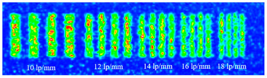
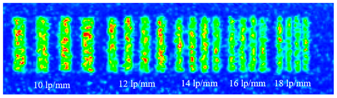
The spatial resolution of the EBAPS is related to the proximity gap between the photocathode and the APS, as well as the electric field intensity. In this experimental setup, the separation distance between the photocathode and APS was 2 mm, and the electric field intensity was 4000 V/mm. To evaluate the spatial resolution of the EBAPS, the cathode must be placed into a resolution line pair using photolithography. As shown in Figure 2a, a semi-transparent gold cathode with different resolution line pairs was deposited on a convex quartz optical window to increase the electric field strength between the gold cathode and the CMOS sensor. For a proximity-focused detector, the resolution improves as the electric field strength increases. The result of electron bombardment spatial resolution with an 8000 V accelerating voltage is shown in Figure 6. From left to right, the resolution is 10, 12, 14, 16 and 18 lp/mm. As shown in the Figure 6, under an electron acceleration voltage of 8000 V, the spatial resolution of the EBAPS can reach 18 lp/mm, which meets most detection needs. The electric field intensity can be increased by reducing the distance, thereby increasing the spatial resolution of the EBAPS.
Figure 6.
Spatial resolution of the electron bombardment image @8000 V accelerating voltage.
3.4. Gain Characteristics with Different Passivation Film Thicknesses
The CMOS chips used in this study had already been packaged and had a passivation layer on the chip surface, typically dozens to hundreds of nanometers thick, to reduce dark current and act as an anti-reflection film. To obtain the desired passivation layer thickness, we used buffered oxide etch to thin out the dielectric film on the CMOS surface. During the wet etching process, we used an ellipsometer to monitor the thickness of the surface passivation layer. After etching, dark noise images of the two passivation layer thicknesses were compared under dark conditions, and no differences in dark noise were observed.
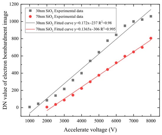
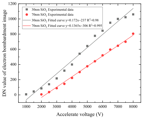
As shown in Figure 7, the DN value of the electron bombardment image with a 30 nm thick passivation layer was higher than that with a 70 nm thick passivation layer. It can be seen in the figure that when the passivation layer was 70 nm thick, there was no obvious electron bombardment gain at 2000 V acceleration voltage. It can be inferred from this result that the energy loss of electrons in the 70 nm thick passivation layer is 2000 eV. As the thickness of the passivation layer decreases to 30 nm, electrons exhibit clear electron multiplication at 2000 V. When the voltage reaches 1000 V, the DN value of the electron bombardment image gradually appears, from which it can be concluded that the energy loss in the 30 nm passivation layer is 1000 eV. This is because when electrons traverse the passivation layer, they collide with the dielectric material and lose energy; more energy is lost as the thickness increases.
Figure 7.
DN value of electron bombardment image with different passivation layer thickness on CMOS chip.
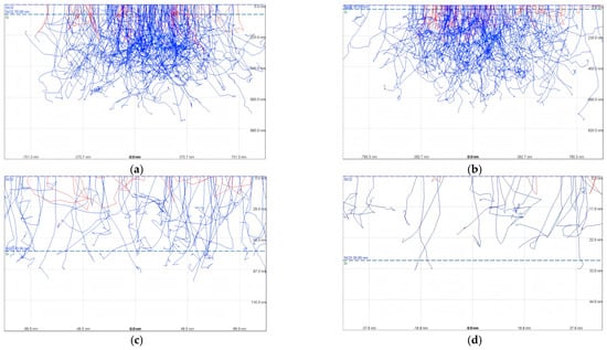
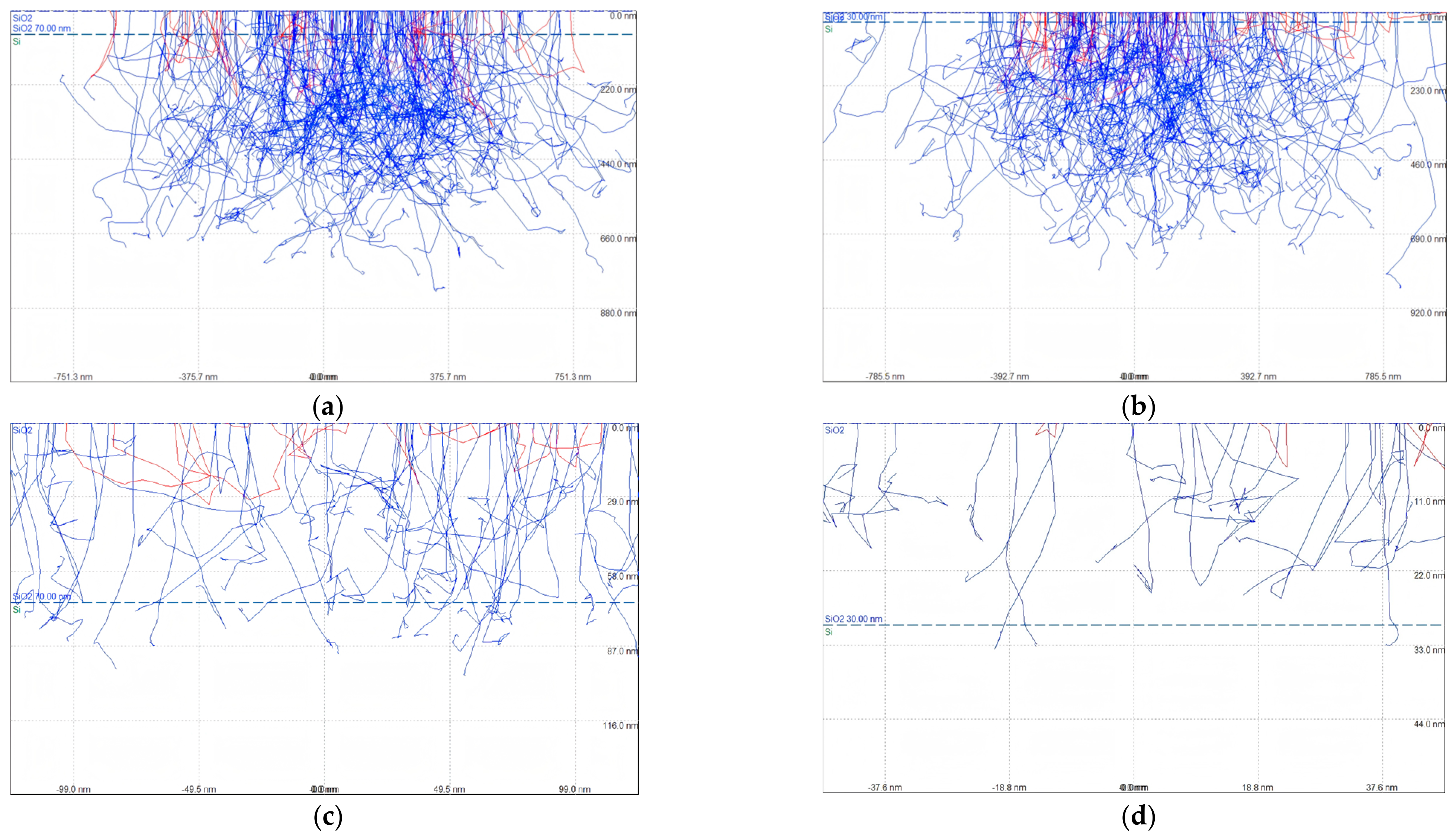
To further verify the influence of different passivation layer thicknesses on the electron bombardment gain, the CASINO (version 2.5.1.0) Monte Carlo electron trajectory simulation software was used to simulate the electron distribution under different passivation layer thicknesses and different voltage conditions. As shown in Figure 8a,b, when the electron bombardment energy is 8000 eV, the transmission depths of the passivation layer at 70 nm and 30 nm are 660 nm and 690 nm, respectively. In Figure 8c, when the accelerating voltage is 2000 V, electrons exhibit residual energy and can enter Si CMOS after passing through the 70 nm passivation layer. According to Figure 8d, after passing through the 30 nm passivation layer, electrons can reach the Si CMOS surface at an accelerating voltage of 1000 V. As shown in Figure 8c,d, the energy losses of electrons passing through the 70 nm and 30 nm passivation layers are close to 2000 eV and 1000 eV, respectively. This is consistent with the results shown in Figure 7.
Figure 8.
Simulation of electron transmission depth. (a) The 70 nm SiO2 passivation layer at 8000 eV. (b) The 30 nm SiO2 passivation layer at 8000 eV. (c) The 70 nm SiO2 passivation layer at 2000 eV. (d) The 30 nm SiO2 passivation layer at 1000 eV.
4. Conclusions
Electron-Bombarded Active Pixel Sensors are a photoelectric hybrid technology that combines the advantages of electric vacuum and semiconductor detectors. In this study, we built a laboratory demonstration system to investigate Electron-Bombarded Active Pixel Sensors. We obtained the linear relationship curve between electron bombardment gain and accelerating voltage. The spatial resolution can reach 18 lp/mm under an 8000 V deceleration voltage when the distance between the photocathode and active pixel sensor anode is 2 mm. By reducing the thickness of the passivation layer from 70 nm to 30 nm, the dead layer loss energy is reduced from 2000 eV to 1000 eV. Furthermore, a Monte Carlo simulation was established and used to explain the experimental results. The established model shows excellent agreement between the experimental results and the theoretically calculated results. These findings are useful for back-thinning and surface treatment of Electron-Bombarded Active Pixel Sensors.
Author Contributions
Conceptualization, Y.B. and J.Z.; methodology, W.C.; software, P.X.; validation, W.C. and Y.Y.; formal analysis, X.B., B.Z. and B.W.; investigation, Y.G. and X.T.; resources, Y.B. and J.Q.; data curation, W.C.; writing—original draft preparation, W.C.; writing—review and editing, Y.B. and J.Z.; visualization, W.C.; supervision, Y.B. and J.Z.; project administration, Y.B. and B.W.; funding acquisition, W.C. and J.Z. All authors have read and agreed to the published version of the manuscript.
Funding
This research was funded by the Chinese Academy of Sciences (YSBR-081), the National Natural Science Foundation of China (Grant No. 61904202, Grant No. 11803074, Grant No. 11675258, Grant No. 61890961), the Strategic Priority Research Program of Chinese Academy of Sciences (Grant No. XDA17010203), and the Youth Innovation Promotion Association XIOPM-CAS.
Institutional Review Board Statement
Not applicable.
Data Availability Statement
The raw data supporting the conclusions of this article will be made available by the authors on request.
Acknowledgments
The authors gratefully acknowledge the financial support from the Chinese Academy of Sciences (YSBR-081), the National Natural Science Foundation of China (Grant No. 61904202, Grant No. 11803074, Grant No. 11675258, Grant No. 61890961), the Strategic Priority Research Program of Chinese Academy of Sciences (Grant No. XDA17010203), and the Youth Innovation Promotion Association XIOPM-CAS. We also thank our supervisor and research members for their valuable advice and experimental assistance. Special thanks go to the anonymous reviewers for their helpful comments to improve this manuscript.
Conflicts of Interest
The authors declare no conflicts of interest. The funders had no role in the design of the study; in the collection, analysis, or interpretation of data; in the writing of the manuscript; or in the decision to publish the results.
Abbreviations
The following abbreviations are used in this manuscript:
| EBAPS | Electron-Bombarded Active Pixel Sensor |
| APS | Active Pixel Sensor |
References
- Lindner, M.B.; Elstein, S.; Lindner, P. Solar Blind and Bispectral Imaging with ICCD, BCCD, and EBCCD Cameras; SPIE: Bellingham, WA, USA, 1998. [Google Scholar] [CrossRef] [Scilit]
- Buontempo, S.; Chiodi, G.; Dalinenko, I.; Ereditato, A.; Ekimov, A.; Fabre, J.; Fedorov, V.; Frenkel, A.; Galeazzi, F.; Garufi, F.; et al. The Megapixel EBCCD: A high-resolution imaging tube sensitive to single photons. Nucl. Instrum. Methods Phys. Res. Sect. A Accel. Spectrometers Detect. Assoc. Equip. 1998, 413, 255–262. [Google Scholar] [CrossRef] [Scilit]
- Carruthers, G.R.; Heckathorn, H.M.; Opal, C.B.; Jenkins, E.B.; Lowrance, J.L. Development of EBCCD Cameras for the Far Ultraviolet. In Advances in Electronics and Electron Physics; Academic Press: Cambridge, MA, USA, 1988; Volume 74, pp. 181–200. [Google Scholar] [CrossRef] [Scilit]
- Auriemma, G.; Errico, L.; Satriano, C.; Vittone, A.A. EBCCD applications in astronomy. Mem. Della Soc. Astron. Ital. 2002, 73, 433–438. [Google Scholar]
- Seitz, P.; Albert, J.; Theuwissen, E. Single-Photon Imaging; Springer Science & Business Media: Berlin/Heidelberg, Germany, 2011. [Google Scholar] [CrossRef] [Scilit]
- Jagutzki, O.; Barnstedt, J.; Spillmann, U.; Spielberger, L.; Mergel, V.; Ullmann-Pfleger, K.; Grewing, M.; Schmidt-Boecking, H.W. Fast-position and time-sensitive readout of image intensifiers for single-photon detection. Int. Soc. Opt. Photonics 1999, 3764, 61–69. [Google Scholar] [CrossRef] [Scilit]
- Bolton, S.J. The Juno Mission. Proc. Int. Astron. Union 2010, 6, 92–100. [Google Scholar] [CrossRef] [Scilit]
- Mende, S.B.; Heetderks, H.; Frey, H.; Lampton, M.; Geller, S.; Habraken, S.; Renotte, E.; Jamar, C.; Rochus, P.; Spann, J.; et al. Far Ultraviolet Imaging from the IMAGE Spacecraft. Space Sci. Rev. 2000, 91, 243–270. [Google Scholar] [CrossRef] [Scilit]
- Darling, N.T.; Siegmund, O.H.W.; Curtis, T.; Jelinsky, S.; McPhate, J.; Tedesco, J. Performance Results of the ICON FUV Sealed Tube Converters; SPIE: Bellingham, WA, USA, 2015. [Google Scholar] [CrossRef] [Scilit]
- Thompson, W.T. UV detectors aboard SOHO. In Proceedings of Spie the International Society for Optical Engineering; SPIE: Bellingham, WA, USA, 1999; p. 3764. [Google Scholar] [CrossRef] [Scilit]
- Daigle, O.; Carignan, C. Extreme faint flux imaging with an EMCCD. Publ. Astron. Soc. Pac. 2009, 121, 866. [Google Scholar] [CrossRef] [Scilit]
- Barbier, R.; Cajgfinger, T.; Calabria, P.; Chabanat, E.; Chaize, D.; Depasse, P.; Doan, Q.; Dominjon, A.; Guérin, C.; Houles, J.; et al. A single-photon sensitive ebCMOS camera: The LUSIPHER prototype. Nucl. Instrum. Methods Phys. Res. Sect. A Accel. Spectrometers Detect. Assoc. Equip. 2011, 648, 266–274. [Google Scholar] [CrossRef] [Scilit]
- Aebi, V.W.; Costello, K.A.; Arcuni, P.W.; Genis, P.G.; Gustafson, S.J. EBAPS®: Next Generation, Low Power, Digital Night Vision. Available online: https://www.semanticscholar.org/paper/EBAPS-®-%3A-Next-Generation%2C-Low-Power%2C-Digital-Night-Aebi-Costello/002b4258a6ebc2bca32cb725a87904ff28a11c09 (accessed on 14 May 2026).
- Moran, S.E.; Ulich, B.L.; Elkins, W.P.; Strittmatter, R.J.; DeWeert, M.J. Intensified CCD (ICCD) Dynamic Range and Noise Performance; SPIE: Bellingham, WA, USA, 1997. [Google Scholar] [CrossRef] [Scilit]
- Feuerbacher, B. Experimental Investigation of Photoemission from Satellite Surface Materials. J. Appl. Phys. 1972, 43, 1563–1572. [Google Scholar] [CrossRef] [Scilit]
- Liu, H.; Wang, X.; Tian, J.; Sai, X.; Wei, Y.; Wen, W.; Wang, J.; Xu, X.; Wang, C.; Lu, Y.; et al. High resolution electron bombareded complementary metal oxide semiconductor sensor for ultraviolet detection. Acta Phys. Sin. 2018, 67, 168–174. [Google Scholar] [CrossRef] [Scilit]
Disclaimer/Publisher’s Note: The statements, opinions and data contained in all publications are solely those of the individual author(s) and contributor(s) and not of MDPI and/or the editor(s). MDPI and/or the editor(s) disclaim responsibility for any injury to people or property resulting from any ideas, methods, instructions or products referred to in the content. |
© 2026 by the authors. Licensee MDPI, Basel, Switzerland. This article is an open access article distributed under the terms and conditions of the Creative Commons Attribution (CC BY) license.