


Abstract
This study presents an all-optical artificial synapse based on 2D perovskite materials for neuromorphic visual simulation. While conventional optoelectronic synapses, which integrate memory and processing, are prevalent in this field, their inherent optical-to-electrical conversion during signal processing incurs significant energy costs. In contrast, our proposed device operates purely in the optical domain. Under ultraviolet–visible light control, the change in light transmittance of this device can simulate various key biological synaptic plasticity behaviors, including paired-pulse facilitation and learning ability. By integrating these devices into a 28 × 28 synaptic array, we constructed an artificial neural network that mimics the experience-driven enhancement characteristic of human visual perceptual learning. Under light-responsive regulation, the system optimized image recognition learning behavior, and after multiple training sessions, the recognition accuracy stabilized above 97%. This study is based on two-dimensional perovskite materials and provides a new material platform for realizing intelligent visual systems with adaptive learning capabilities.
1. Introduction
Vision is the primary way humans understand the environment, with more than 80% of external information obtained through vision. This makes it far more important than other perception pathways such as hearing and touch [1]. As a fundamental sense, vision detects light signal patterns from the environment, interprets and transforms them, and ultimately forms image cognition [2]. The complex visual system endows humans with advanced visual perception, allowing us to identify and perceive the surface properties of objects through their size, shape, color, brightness, distance, sense of position, smoothness, and roughness [3,4]. Perceptual learning, as an important manifestation of neuroplasticity in the human brain, enables significant improvement in multiple perceptual abilities, such as contrast, orientation, direction of movement, and texture density discrimination [5]. Therefore, simulated visual perception learning is an important basis for constructing neuromorphic artificial vision systems. In the human brain, this process is closely related to the phenomenon of perceptual learning, where the perceptual system enhances its response to specific stimuli through learning experiences, and the time required to relearn lost skills is reduced. Traditional vision systems are mostly based on the von Neumann architecture, and the physical separation of storage and processing units leads to high energy consumption when performing highly complex and abstract computing tasks [6]. To address this challenge, researchers are exploring a technical approach that integrates neuromorphic computing devices based on artificial synapses with artificial neural networks [7,8].
At present, optoelectronic synapses in artificial synapses are a research hotspot. Optoelectronic synapses [9,10,11] can directly simulate synaptic functions using optical signals [12,13,14,15] and demonstrate significant advantages in feature recognition and dynamic responses to environmental stimuli such as light and electricity [16,17]. By leveraging their plastic learning mechanisms, these synapses can effectively filter key feature information from visual data. After extracted feature information is input into artificial neural networks, efficient image recognition can be achieved, forming the core capability of artificial visual perception systems. However, most existing optoelectronic synapse devices rely on electrical signals in their computational core [18,19]. Due to their dependence on wired circuit architectures and lack of wireless transmission capabilities, these devices limitations in terms of response speed and energy efficiency [20]. In contrast, all-optical artificial synapses realize stimulus-response measurements through purely optical control, offering a solution for optical signal recognition.
In recent years, significant progress has been made in the research of all-optical control of synapses. Zhuge et al. demonstrated an all-optical memristor based on InGaZnO materials, in which the device conductance could be reversibly adjusted over a continuous range by changing the wavelength of the control light, and the multiple conductance states induced by light were non-volatile [21]. Feldmann et al. integrated an all-optical neural network onto a millimeter-scale photonic chip, regulating synaptic weights via the light absorption of phase-change materials, and successfully demonstrated both supervised and unsupervised learning capabilities [22]. The approaches used in these studies for synaptic weight modulation, whether through wavelength-dependent conductance control or by utilizing the optical response of phase-change materials, are consistent with the strategy employed in this study, which simulates synaptic plasticity by controlling the transmittance of (PEA)2PbI4 thin films using optical signals, although in this study synaptic weights are characterized by the optical parameter of transmittance.
In this paper, all-optical artificial synapses were fabricated using 2D (PEA)2PBI4 perovskite films. The transmittance of these synapses can be modulated by light pulses, and based on this optically driven mechanism, various neural synaptic functions such as paired-pulse facilitation, short-term and long-term memory, and learning behaviors were successfully simulated [23,24,25,26,27]. Utilizing this property, a brain-like visual learning system can be constructed with 2D (PEA)2PBI4 perovskite films, in which the photoresponse characteristics are precisely controlled by adjusting the number, power, wavelength, and frequency of ultraviolet light. A 28 × 28 synapse array artificial neural network (ANN) was constructed to simulate the human visual perception and learning system. Under optical response modulation, this system can optimize image recognition learning and memory behaviors, with recognition accuracy stabilizing above 97% after multiple learning sessions. The present work continues and expands the research direction of all-optical neuromorphic vision systems. Since the early demonstrations of all-optical synapses and subsequent reports on neurosynaptic networks with learning capabilities [22,28], this field has been gradually progressed from theory to practice. This study, based on photochromic perovskite materials, supplements this direction with an implementation scheme based on the photochromic properties of the materials.
2. Materials and Methods
2.1. Preparation of (PEA)2PBI4 Solution and Films
The (PEA)2PBI4 perovskite solution was prepared using a one-step method. 1 mole of PEAI and 0.5 mole of PbI2 powder were dissolved in 1 mL of DMF solvent, and stirred continuously at 50 °C and 900 r/min for two hours to prepare a 0.5 mol/L (PEA)2PBI4 solution for use. PEAI, PbI2, and DMF were all purchased from Shanghai Aladdin Biochemical Technology Co., Ltd. (Located in Shanghai, China); all materials were used without further purification. The prepared perovskite solution was spin-coated onto hydrophilic-treated glass substrates at 2500 r/min for 30 s, and the resulting film was annealed on a hot plate at 100 °C for 10 min. The entire experiment was conducted in a water-free and oxygen-free glove box.
2.2. Real-Time Light Transmittance Measurement of (PEA)2PBI4 Thin Films
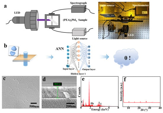
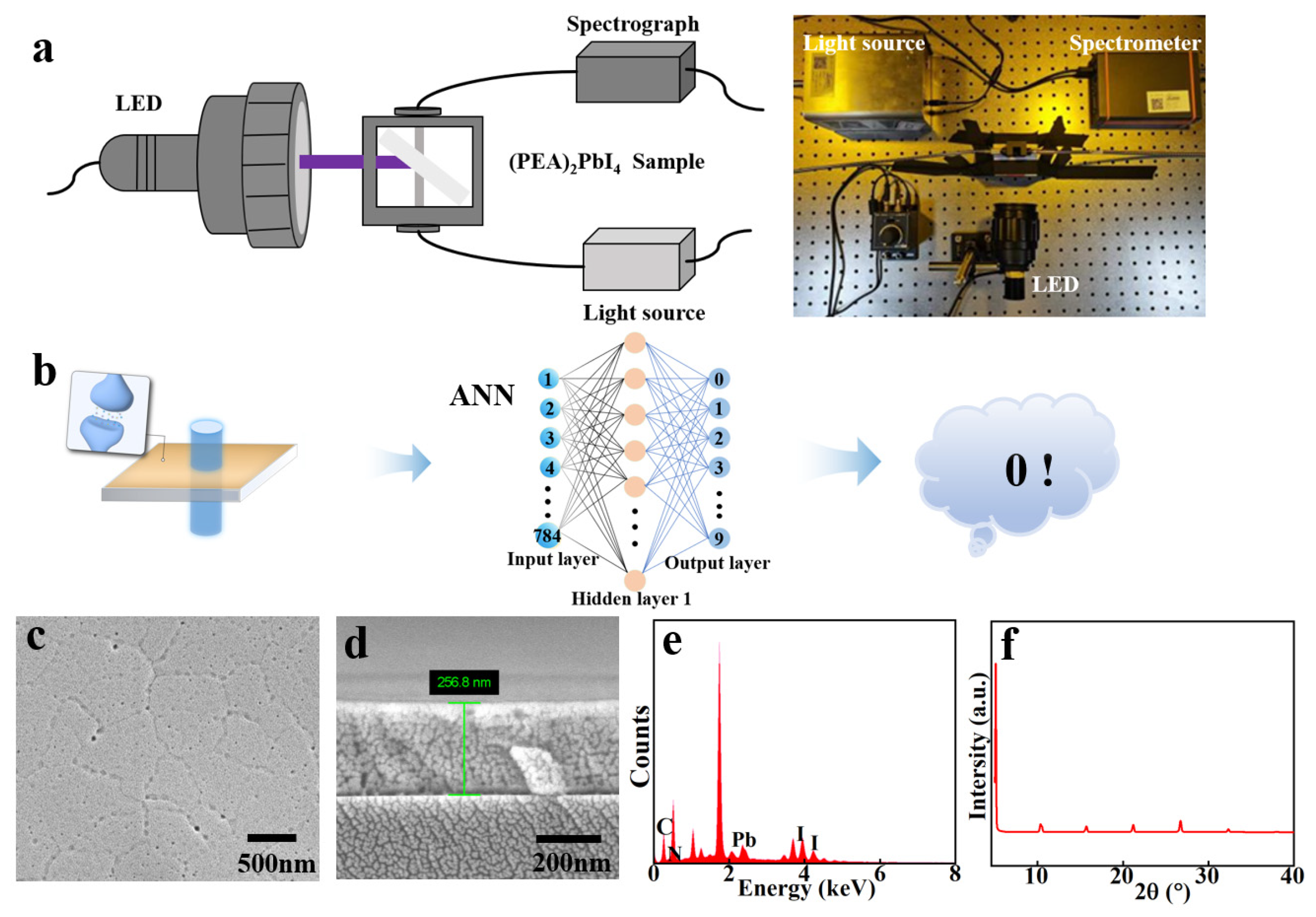
The real-time transmittance change data of the all-optical synapses based on (PEA)2PBI4 perovskite were collected using a custom-built real-time transmittance measurement system. As shown in Figure 1a, a high-speed spectrometer (AvaSpec-ULS2048CL-EVO, AVANTES) was used in this system to detect the real-time transmittance changes in the (PEA)2PBI4 all-optical synaptic device when receiving and removing light pulses. The measurement setup consists of a 365 nm ultraviolet LED, a collimating lens assembly for adjusting the light spot size, a three-sided transparent sample holder for fixing the sample position, and a white light compensation source. The real-time light transmittance change (ΔT) is measured using the high-speed CMOS spectrometer (model: Avaspec-ULS2048CL-EVO) based on the transmittance difference at a wavelength of 517 nm. The adjustable collimating adapter allows the LED output spot size to be freely adjusted, and its output power can also be freely adjusted via the LED driver.
Figure 1.
(PEA)2PBI4 perovskite thin film optical testing system schematic and all-optical synapse schematic and material characteristics. (a) Schematic of the (PEA)2PBI4 perovskite thin film optical testing system. (b) Schematic of the (PEA)2PBI4 perovskite thin film all-optical synapse, showing the recognition process. (c) Scanning electron microscope (SEM) surface image of the (PEA)2PBI4 perovskite thin film. (d) Cross-sectional SEM image of the (PEA)2PBI4 perovskite thin film. (e) Energy spectrum analysis of the (PEA)2PBI4 perovskite thin film. (f) X-ray diffraction (XRD) pattern of the (PEA)2PBI4 perovskite thin film.
2.3. Design of Artificial Neural Networks
For the neural network’s training and evaluation, a subset of the National Institute of Standards and Technology Hybridization (MNIST) database was utilized, comprising 20,000 grayscale images (28 × 28 pixels) of handwritten digits (0–9) for training and 10,000 for testing. The network architecture features an input layer of 784 neurons, corresponding to the image pixels, and an output layer of 10 neurons. To generate the test data for image recognition, the transmittance change in samples at 517 nm was measured after varying UV exposure durations. A grayscale value of 255 was assigned to the transmittance change induced by five cycles of 30 s UV exposure, each followed by a 10 s pause. All other grayscale values were determined based on a linear relationship with the measured transmittance changes. The recognition algorithm was implemented in Python (Python 3.8), employing stochastic gradient ascent/descent for synaptic weight updates. The simulation parameters included a learning rate of 0.01, a target error of 1 × 10⁻³, and a sigmoid activation function on the output neurons to constrain signals between 0 and 1.
3. Results and Discussion
3.1. All-Optical Synapse Mechanism and Materia Characterization of Perovskite Thin Films
Traditional optoelectronic synapse systems usually rely on photocurrent conduction, and their energy loss and signal crosstalk issues limit system efficiency. In this paper, we focus on an all-optical artificial synapse mechanism based on (PEA)2PbI4 perovskite thin films. Under 365 nm laser stimulation, these films exhibit persistent and tunable changes in transmittance without generating electrical current. This behavior effectively mimics the synaptic weight modulation observed in biological neurons.
The observed photoinduced transmittance variation in (PEA)2PBI4 films can be attributed to multiple interrelated physical processes, as supported by both our experimental results and existing literature. Photoinduced lattice expansion serves as a direct origin of the transmittance change; Cuthriell et al. observed a 0.37% expansion along the c-axis upon photoexcitation, with the associated bandgap redshift leading to a shift in the absorption edge [29]. The filling of defect states contributes to wavelength selectivity. Yin et al. demonstrated that iodine vacancies can function as optically active centers, thereby modulating absorption characteristics [30], while Kahmann et al. found that shallow level defects also participate in these optical processes [31]. Additionally, ion migration plays a role in the medium-timescale response. Zhang et al. reported that ion migration induces a shift of 2–3 nm in the absorption peak [32]. In our experiments, the difference in the magnitude of transmittance changes induced by ultraviolet and visible light is attributed to the selective activation of defect states at varying depths, and certain reversible behaviors are consistent with the characteristics of ion migration. Together, these mechanisms synergistically give rise to the photoinduced transmittance variation observed in (PEA)2PBI4 films.
Based on this, we constructed an all-optical perception-processing system in which the optical state changes in the film directly serve as input signals for an ANN. This system successfully achieved accurate recognition of the digit “0” in optical images (Figure 1b). This work provides a new approach for developing low-power, highly parallel neuromorphic visual perception systems.
The surface and cross-sectional morphology of the (PEA)2PBI4 films were examined using field emission scanning electron microscopy (SEM). As shown in Figure 1c, the SEM images of the surface display a uniform distribution of particles with no obvious cracks. The cross-sectional images confirm that the film thickness is approximately 256.8 nm (Figure 1d). Energy-dispersive spectroscopy (EDS) combined with SEM indicates the presence of characteristic elements in the sample, including lead (Pb), iodine (I), carbon (C), and nitrogen (N) (Figure 1e). The phase of the (PEA)2PBI4 films was characterized using X-ray diffraction (XRD). Diffraction peaks were observed at 2θ angles of 5.1°, 10.38°, 15.74°, 21.18°, and 26.78°, with no additional peaks corresponding to impurity phases detected, indicating high phase purity (Figure 1f).
3.2. Optical Properties and Synaptic Characteristics Verification of (PEA)2PBI4 Perovskite Films
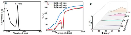
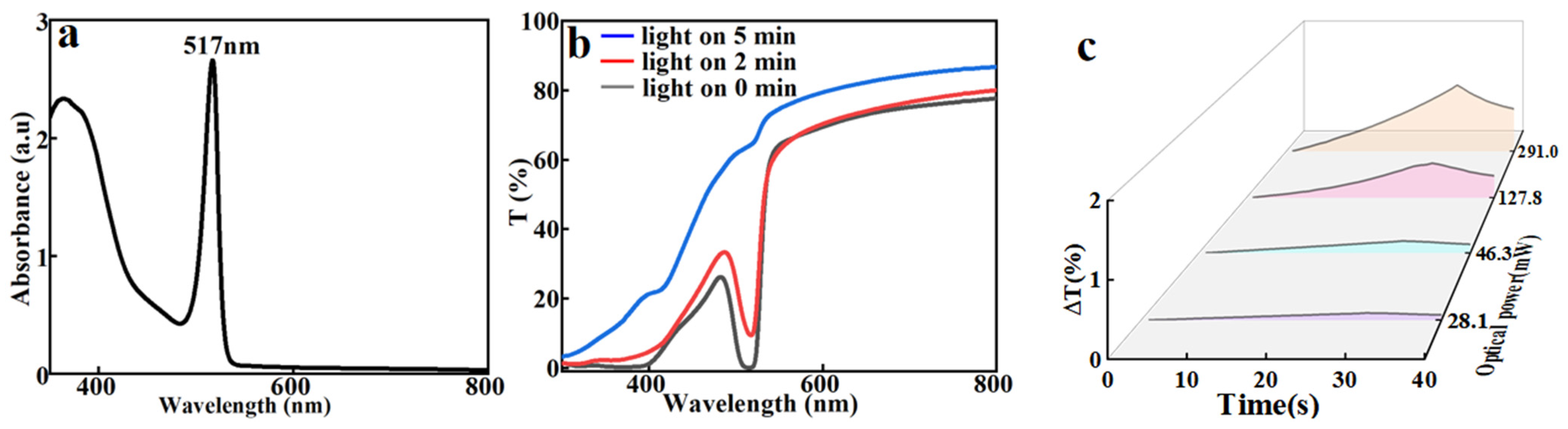
The optical properties of the (PEA)2PBI4 perovskite films are presented in Figure 2a. Ultraviolet–visible (UV-Vis) absorption spectroscopy reveals that the (PEA)2PBI4 perovskite exhibits an absorption peak at 517 nm within the wavelength range of 300–800 nm, indicating that the material has the strongest light absorption at this wavelength. Figure 2b shows the real-time transmittance changes in the film under 365 nm ultraviolet light (291 mW) irradiation for different durations (0 min, 2 min and 5 min). The real-time transmittance continuously increases with prolonged irradiation time. The change in transmittance at 517 nm is the most pronounced and coincides with the absorption peak position. Therefore, this wavelength was selected for subsequent measurements. In Figure 2c, the films were irradiated with 365 nm ultraviolet light at different powers (28.1 mW, 46.3 mW, 127.8 mW and 291 mW) for 30 s, followed by 10 s light-off periods. The results show that at 517 nm, the increase in real-time transmittance is the largest, and the rate of transmittance change increases with higher light power. In summary, at a wavelength of 517 nm, higher light irradiation power leads to a more significant real-time transmittance change in the film.
Figure 2.
Optical properties of (PEA)2PBI4 perovskite films. (a) Absorption spectrum of (PEA)2PBI4 perovskite films in the steady state from 300 nm to 800 nm. (b) Light transmittance variation curves of (PEA)2PBI4 perovskite films at a wavelength of 517 nm under 365 nm UV light (291 mW) irradiation for different durations. (c) Real-time transmittance variation curves of (PEA)2PBI4 perovskite films at a wavelength of 517 nm under 365 nm UV light of different powers for the same duration.
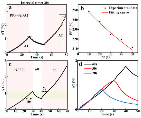
Plasticity is a fundamental property of biological synapses and serves as the physiological basis for learning and memory. This dynamic characteristic allows synapses to perform diverse functions during information processing. Depending on the duration, synaptic plasticity can be classified into short-term memory (STM) and long-term memory (LTM). In visual information processing, paired-pulse facilitation (PPF) is a typical form of plasticity, where the response to the second of two consecutive stimuli depends strongly on the time interval between them. As shown in Figure 3a, A1 and A2 represent the transmittance changes induced by the first and second light pulses, respectively, the PPF index is defined as the ratio A2/A1. Figure 3b presents the PPF characteristics of an all-optical perovskite synaptic device under 365 nm ultraviolet light excitation. The results show that the PPF index varies with the pulse interval (Δt). This trend can be fitted by a double-exponential function [33,34]:
where C1 and C2 are the initial facilitation, t1 and t2 are the characteristic relaxation time of the decay term. The fitting results indicate that t2 (182 s) is approximately one order of magnitude larger than t1 (79 s), which is consistent with reported data from biological synapses [35]. The response speed is characterized by the relaxation time constants t1 and t2, where fast relaxation corresponds to short-term memory decay and slow relaxation reflects long-term memory retention. To clarify the technical positioning of this work, we compare the relaxation times with recently reported all-optical synaptic devices. The CsPbBr3 single-crystal device from Shandong University has relaxation times of t1 = 0.52 s and t2 = 7.09 s [36]. In another study, relaxation characteristics with t1 = 11.5 s and t2 = 689.4 s were reported, demonstrating ultra-long memory retention of approximately 11.5 min [27]. In the present work, the (PEA)2PbI4 based device shows measured relaxation times of t1 = 79 s and t2 = 182 s. The slow relaxation time is about 25 times longer than that of CsPbBr3 device, placing it in the medium memory duration range of about 3 min, between fast response and ultra-long memory. This provides a more adaptable material choice for visual perception scenarios requiring moderate information retention.
PPF = 1 + C1 ∗ exp(−∆t/t1) + C2 ∗ exp(−∆t/t2)
Figure 3.
Synaptic properties of all-optical synapses based on (PEA)2PBI4 perovskite films. (a) PPF behavior under stimulation with a 291 mW, 365 nm ultraviolet light beam. (b) Fitting curve of the PPF index versus interval. (c) Simulation of the human brain’s learning-forgetting-relearning process under 291 mW, 365 nm UV light stimulation. (d) Different durations of continuous illumination under 291 mW, 365 nm UV light (continuous illumination times of 20 s, 30 s, and 40 s, respectively).
The “learning-forgetting-relearning” process in the human brain is an important component of human cognitive activity. During the learning phase, the brain processes and stores information by forming new synaptic connections or strengthening existing ones, which is reflected as an increase in synaptic weight. In the forgetting phase, synaptic weights gradually weaken, and related memories fade over time. During the relearning process, existing neural connections can be reactivated, allowing the brain to relearn knowledge more rapidly based on previously established synaptic foundations and to form more lasting memories.
As shown in Figure 3c, two 365 nm ultraviolet light pulses with intervals of 10 s and pulse widths of 30 s were used to induce transmittance changes in the (PEA)2PBI4 films. Under the first light pulse stimulation, corresponding to the initial learning process, the transmittance change in the film increased by 1.10112% over 30 s. After the light pulse stimulation was removed, representing the memory forgetting process, the transmittance change gradually decreased to 0.6557% over time. When the light pulse stimulation was applied again to the same film, representing the relearning process, it took only 7 s for the transmittance change to recover from the decayed value of 0.6557% to 1.10112%. In contrast, during the first learning process, reaching the same increase from 0.6557% to 1.10112% required 10 s, indicating that the relearning time is shorter than the first learning time. Furthermore, under the same 30 s light pulse stimulation, the transmittance change in the film during the second stimulation reached a higher value of 2.67451%. This enhanced learning behavior enables the effective extraction of useful visual information and supports high-precision recognition, closely resembling the characteristics of a visual perception learning system.
The conversion between STM and LTM is a dynamically regulated process. High-frequency or continuous stimulation can gradually transform STM into LTM, which is reflected in the persistence of enhanced synaptic strength. The results presented in Figure 3d indicate that the duration of continuous illumination can simulate the transition from STM to LTM, suggesting that stimulation duration is a key parameter affecting memory retention. These findings confirm that (PEA)2PBI4 perovskite synaptic devices can accurately replicate the dynamic characteristics of biological memory systems by the modulation of synaptic plasticity parameters.
3.3. Simulation of Visual Perception Learning for Perovskite Photochromic Films
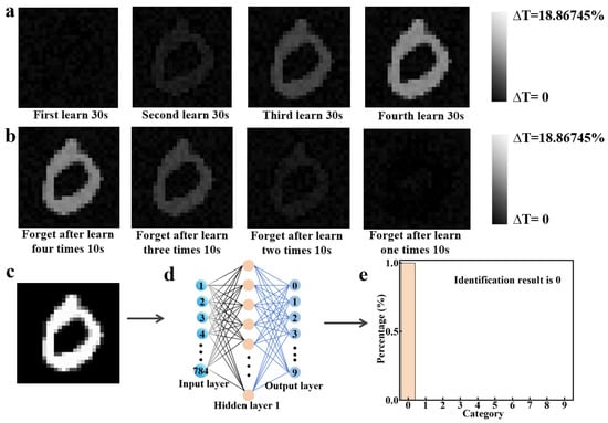
The all-optical synaptic device based on (PEA)2PBI4 perovskite realizes the bionic image recognition function of retinal-like neural network and simulates the perceptual learning mechanism of biological vision system. We measured the real-time light transmittance of (PEA)2PBI4 all-optical synapses at different pulse counts, and then simulated an optical image of the digit “0” corresponding to a 28 × 28 photocurrent array from the MNIST dataset. Figure 4a presents the grayscale images of the digit “0” generated by laser stimulation of 1, 2, 3 and 4 pulses with a width of 30 s. Under a single pulse, the image exhibits poor resolution and darker pixels. As the pulse number increases, the image becomes progressively clearer and brighter. This improvement in image resolution with increasing pulse count can be interpreted as a perceptual learning process. As shown in Figure 4b, the image resolution gradually degrades over time during the forgetting phase, resembling the way the human brain gradually forgets a learned visual pattern.
Figure 4.
Image recognition process of a full-optical artificial synapse array using (PEA)2PBI4 perovskite. (a) Grayscale images of the handwritten digit ‘0’ over time under different numbers of 365 nm laser pulse stimulations. (b) Grayscale images of the ‘0’ forgetting process over time after 365 nm pulse sequence stimulation. (c) Grayscale image of the input 28 × 28 pixel handwritten digit ‘0’. (d) Recognition using an artificial neural network during the image process. (e) Weight map simulated by the artificial neural network.
To further investigate perceptual learning on MNIST handwritten digits, we constructed an artificial neural network comprising a 28 × 28 synaptic array and 10 output neurons. Figure 4c,d illustrate a grayscale image of the digit “0” (28 × 28 pixels) and the corresponding network structure, where the input layer consists of 784 pixels and the output layer represents digits 0 through 9. The image recognition results after five laser pulses are shown in Figure 4e. The probability distribution across the output neurons indicates the likelihood of each digit. Since the probability for the digit “0” is the highest, the network successfully classifies the input image as the digit “0”.
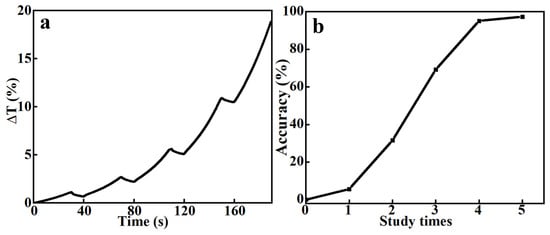
Using an artificial neural network, we demonstrate that sensory responsiveness can be enhanced through repeated exposure, which is a key characteristic of perceptual learning. The transmittance changes in a (PEA)2PBI4 perovskite film under five consecutive 365 nm laser pulses, each with a duration of 30 s are shown in Figure 5a. Figure 5b shows the corresponding recognition accuracy on 10,000 test images from the MNIST dataset under the same optical power but with varying pulse numbers. The results show a clear improvement in accuracy as the pulse count increases. The recognition accuracy rises from 5.65% after a single pulse to 97.35% after five pulses. The accuracy after five pulse stimulations is approximately 17.23 times that after a single pulse. With the continuous increase in the number of laser pulses, the image recognition accuracy continues to improve, which is similar to the human mechanism of continual learning and the deepening of memory with knowledge acquisition.
Figure 5.
Perceptual learning demonstration. (a) Transmittance change curves of (PEA)2PBI4 perovskite films stimulated with six 365 nm laser pulses, each 30 s long. (b) Effect of different numbers of laser pulses at the same power on image recognition accuracy.
4. Conclusions
An all-optical artificial synapse device was successfully developed based on (PEA)2PBI4 perovskite thin films. The device exhibits unique neuromorphic response characteristics under optical stimulation: upon ultraviolet–visible light illumination, the thin film’s optical transmittance changes significantly due to the dynamic reconstruction of the perovskite structure; when the light is turned off, this change gradually decays, mimicking the plasticity behavior of biological synapses. Through systematic optoelectronic characterization, we confirmed that the device can achieve a variety of neuromorphic functions, including short-term/long-term memory (STM/LTM), paired-pulse facilitation (PPF), enhanced learning ability, and logic information processing—key features of neural synapses. By integrating these synaptic devices into an artificial neural network, we constructed a biomimetic visual system with perceptual learning capabilities. After five 30 s laser training pulses, the system achieved a recognition accuracy of 97.35% for the MNIST handwritten digits. This work provides an important reference for developing novel neuromorphic optoelectronic devices, and highlights the potential of optically controlled synapses in building efficient artificial intelligence perception systems.
Author Contributions
Conceptualization, F.L. and Q.H.; methodology, Q.H.; software, F.L.; validation, F.L.; formal analysis, F.L. and R. L; investigation, F.L. and R.L.; resources, Q.H.; data curation, F.L. and R.L.; writing—original draft preparation, F.L.; writing—review and editing, Q.H.; visualization, F.L.; supervision, Q.H.; project administration, Q.H.; funding acquisition, Q.H. All authors have read and agreed to the published version of the manuscript.
Funding
This research was funded by the National Natural Science Foundation of China, grant number 52401057.
Data Availability Statement
The data presented in this study are available on request from the corresponding author.
Conflicts of Interest
The authors declare no conflicts of interest.
References
- Han, X.; Xu, Z.S.; Wu, W.Q.; Liu, X.H.; Yan, P.G.; Pan, C.F. Recent progress in optoelectronic synapses for artificial visual-perception system. Small Struct. 2020, 1, 2000029. [Google Scholar] [CrossRef] [Scilit]
- Ji, X.; Zhao, X.; Tan, M.C.; Zhao, R. Artificial Perception Built on Memristive System: Visual, Auditory, and Tactile Sensations. Adv. Intell. Syst. 2020, 2, 1900118. [Google Scholar] [CrossRef] [Scilit]
- Quiroga, R.Q.; Reddy, L.; Kreiman, G.; Koch, C.; Fried, I. Invariant Visual Representation by Single Neurons in the Human Brain. Nature 2005, 435, 1102–1107. [Google Scholar] [CrossRef] [Scilit] [PubMed]
- Sligte, I.G.; Vandenbroucke, A.R.E.; Scholte, H.S.; Lamme, V.A.F. Detailed Sensory Memory, Sloppy Working Memory. Front. Psychol. 2010, 1, 175. [Google Scholar] [CrossRef] [Scilit] [PubMed]
- Fahle, M. Perceptual Learning: Specificity versus Generalization. Curr. Opin. Neurobiol. 2005, 15, 154–160. [Google Scholar] [CrossRef] [Scilit]
- Choi, C.; Leem, J.; Kim, M.; Taqieddin, A.; Cho, C.; Cho, K.W.; Lee, G.J.; Seung, H.; Bae, H.J.; Song, Y.M.; et al. Curved neuromorphic image sensor array using a MoS2-organic heterostructure inspired by the human visual recognition system. Nat. Commun. 2020, 11, 5934. [Google Scholar] [CrossRef] [Scilit] [PubMed]
- Seo, S.; Lee, J.J.; Lee, H.J.; Lee, H.W.; Oh, S.; Lee, J.J.; Heo, K.; Park, J.H. Recent progress in artificial synapses based on two-dimensional van der Waals materials for brain-inspired computing. ACS Appl. Electron. Mater. 2020, 2, 371–388. [Google Scholar] [CrossRef] [Scilit]
- Wang, Y.; Yin, L.; Huang, W.; Li, Y.Y.; Huang, S.; Zhu, Y.Y.; Yang, D.; Pi, X.D. Optoelectronic synaptic devices for neuromorphic computing. Adv. Intell. Syst. 2021, 3, 2000099. [Google Scholar] [CrossRef] [Scilit]
- Li, R.Z.; Dong, Y.B.; Qian, F.S.; Xie, Y.Y.; Chen, X.; Zhang, Q.M.; Yue, Z.J.; Gu, M. CsPbBr3/graphene nanowall artificial optoelectronic synapses for controllable perceptual learning. PhotoniX 2023, 4, 4. [Google Scholar] [CrossRef] [Scilit]
- Wan, Z.F.; Zhang, Q.W.; Hu, F.Z.; Dong, Y.B.; Li, R.Z.; Hu, L.C.; Xie, Y.Y.; Yue, Z.J.; Chen, X.; Gu, M. Topological insulator optoelectronic synapses for high-accuracy binary image recognition using recurrent neural networks. Adv. Opt. Mater. 2023, 11, 2201852. [Google Scholar] [CrossRef] [Scilit]
- Zhu, Q.B.; Li, B.; Yang, D.D.; Liu, C.; Feng, S.; Chen, M.L.; Sun, Y.; Tian, Y.N.; Su, X.; Wang, X.M.; et al. A flexible ultrasensitive optoelectronic sensor array for neuromorphic vision systems. Nat. Commun. 2021, 12, 1798. [Google Scholar] [CrossRef] [Scilit] [PubMed]
- Liang, K.; Wang, R.; Huo, B.B.; Ren, H.H.; Li, D.W.; Wang, Y.; Tang, Y.J.; Chen, Y.T.; Song, C.Y.; Li, F.F.; et al. Fully printed optoelectronic synaptic transistors based on quantum dot–metal oxide semiconductor heterojunctions. ACS Nano 2022, 16, 8651–8661. [Google Scholar] [CrossRef] [Scilit] [PubMed]
- Li, Y.Y.; Wang, Y.; Yang, D.R.; Pi, X.D. Research progress on optoelectronic synaptic devices. Sci. Sin. Inform. 2020, 50, 892–912. [Google Scholar]
- Wang, Y.; Lv, Z.Y.; Chen, J.R.; Wang, Z.P.; Zhou, Y.; Zhou, L.; Chen, X.L.; Han, S.T. Photonic synapses based on inorganic perovskite quantum dots for neuromorphic computing. Adv. Mater. 2018, 30, 1802883. [Google Scholar] [CrossRef] [Scilit]
- Chen, K.; Hu, H.; Song, I.H.; Cobeze, H.B.; Lee, W.J.; Abtahi, A.K.; Schanze, K.S.; Mei, J.G. Organic optoelectronic synapse based on photon-modulated electrochemical doping. Nat. Photon. 2023, 17, 629–937. [Google Scholar] [CrossRef] [Scilit]
- Liu, K.; Zhang, T.; Dang, B.J.; Bao, L.; Xu, L.Y.; Cheng, C.D.; Yang, Z.; Huang, R.; Yang, Y.C. An optoelectronic synapse based on α-In2Se3 with controllable temporal dynamics for multimode and multiscale reservoir computing. Nat. Electron. 2022, 5, 761–773. [Google Scholar] [CrossRef] [Scilit]
- Ahmed, T.; Kuriakose, S.; Mayes, E.L.; Ramanathan, R.; Bansal, V.; Bhaskaran, M.; Sriram, S.; Walia, S. Optically stimulated artificial synapse based on layered black phosphorus. Small 2019, 15, 1900966. [Google Scholar] [CrossRef] [Scilit]
- Zhou, F.C.; Zhou, Z.; Chen, J.W.; Choy, T.H.; Wang, J.L.; Zhang, N.; Lin, Z.Y.; Yu, S.M.; Kang, J.F.; Wong, H.-S.P.; et al. Optoelectronic resistive random access memory for neuromorphic vision sensors. Nat. Nanotechnol. 2019, 14, 776–782. [Google Scholar] [CrossRef] [Scilit]
- Gao, S.; Liu, G.; Yang, H.L.; Hu, C.; Chen, Q.L.; Gong, G.D.; Xue, W.H.; Yi, X.H.; Shang, J.; Li, R.W. An oxide Schottky junction artificial optoelectronic synapse. ACS Nano 2019, 13, 2634–2642. [Google Scholar] [CrossRef] [Scilit]
- Yang, R.Q.; Wang, Y.; Li, S.Q.; Hu, D.; Chen, Q.J.; Zhuge, F.; Ye, Z.Z.; Pi, X.D.; Lu, J.G. All-Optically Controlled Artificial Synapse Based on Full Oxides for Low-Power Visible Neural Network Computing. Adv. Funct. Mater. 2024, 34, 2312444. [Google Scholar] [CrossRef] [Scilit]
- Hu, L.X.; Yang, J.; Wang, J.R.; Cheng, P.H.; Chua, L.O.; Zhuge, F. All-Optically Controlled Memristor for Optoelectronic Neuromorphic Computing. Adv. Funct. Mater. 2021, 31, 2005582. [Google Scholar] [CrossRef] [Scilit]
- Feldmann, J.; Youngblood, N.; Wright, C.D.; Bhaskaran, H.; Pernice, W.H.P. All-optical spiking neurosynaptic networks with self-learning capabilities. Nature 2019, 569, 208–214. [Google Scholar] [CrossRef] [Scilit] [PubMed]
- Zhou, X.; Hu, F.; Hou, Q.; Hu, J.; Wang, Y.; Chen, X. All-Photonic Artificial Synapses Based on Photochromic Perovskites for Noncontact Neuromorphic Visual Perception. Commun. Mater. 2024, 5, 116. [Google Scholar] [CrossRef] [Scilit]
- Sun, Y.; Wang, H.; Xie, D. Recent advance in synaptic plasticity modulation techniques for neuromorphic applications. Nano-Micro Lett. 2024, 16, 211. [Google Scholar] [CrossRef] [Scilit]
- Goi, E.; Zhang, Q.; Chen, X.; Luan, H.; Gu, M. Perspective on photonic memristive neuromorphic computing. PhotoniX 2020, 1, 3. [Google Scholar] [CrossRef] [Scilit]
- Shastri, B.J.; Tait, A.N.; Ferreira de Lima, T.; Pernice, W.H.P.; Bhaskaran, H.; Wright, C.D.; Prucnal, P.R. Photonics for artificial intelligence and neuromorphic computing. Nat. Photon. 2021, 15, 102–114. [Google Scholar] [CrossRef] [Scilit]
- Hu, F.; Ma, X.; Chen, X. All-optical synapses enabled by photochromic materials for high-accuracy optical signal recognition. Adv. Opt. Mater. 2025, 12, 2637–2646. [Google Scholar] [CrossRef] [Scilit]
- Gholipour, B.; Bastock, P.; Craig, C.; Khan, K.; Hewak, D.; Soci, C. Amorphous metal-sulphide microfibers enable photonic synapses for brain-like computing. Adv. Opt. Mater. 2015, 3, 635–641. [Google Scholar] [CrossRef] [Scilit]
- Cuthriell, S.A.; Panuganti, S.; Laing, C.C.; Quintero, M.A.; Guzelturk, B.; Yazdani, N.; Traore, B.; Brumberg, A.; Malliakas, C.D.; Lindenberg, A.M.; et al. Nonequilibrium Lattice Dynamics in Photoexcited 2D Perovskites. Adv. Mater. 2022, 34, 2202709. [Google Scholar] [CrossRef] [Scilit]
- Yin, J.; Naphade, R.; Gutiérrez-Arzaluz, L.; Brédas, J.-L.; Bakr, O.M.; Mohammed, O.F. Modulation of Broadband Emissions in Two-Dimensional ⟨100⟩-Oriented Ruddlesden–Popper Hybrid Perovskites. ACS Energy Lett. 2020, 5, 2149–2155. [Google Scholar] [CrossRef] [Scilit]
- Kahmann, S.; Duim, H.; Fang, H.H.; Dyksik, M.; Adjokatse, S.; Medina, M.R.; Pitaro, M.; Plochocka, P.; Loi, M.A. Photophysics of Two-Dimensional Perovskites—Learning from Metal Halide Substitution. Adv. Funct. Mater. 2021, 31, 2103778. [Google Scholar] [CrossRef] [Scilit]
- Zhang, P.Y.; Su, W.L.; Yang, Y.B.; Jiang, X.F.; Zhang, W.K. Influence of Intermolecular Interactions on Ion Migration at 2D/3D Perovskite Interfaces. Chin. J. Chem. Phys. 2025, 38, 649–658. [Google Scholar] [CrossRef] [Scilit]
- Yin, L.; Han, C.; Zhang, Q.; Ni, Z.; Zhao, S.; Wang, K.; Li, D.; Xu, M.; Wu, H.; Pi, X.; et al. Synaptic silicon-nanocrystal phototransistors for neuromorphic computing. Nano Energy 2019, 63, 103859. [Google Scholar] [CrossRef] [Scilit]
- Yang, C.S.; Shang, D.S.; Liu, N.; Shi, G.; Shen, X.; Yu, R.C.; Li, Y.Q.; Sun, Y. A synaptic transistor based on quasi-2D molybdenum oxide. Adv. Mater. 2017, 29, 1700906. [Google Scholar] [CrossRef] [Scilit]
- Chang, T.; Jo, S.-H.; Lu, W. Short-term memory to long-term memory transition in a nanoscale memristor. ACS Nano 2011, 5, 7669–7676. [Google Scholar] [CrossRef] [Scilit]
- Cheng, P.P.; Liu, Z.H.; Zhou, J.; Kang, P.; Wang, X.; Li, X.; Zhao, X.; Zhao, J.; Zuo, Z. All-Optical Excitatory and Inhibitory Synapses Based on Reversible Photo-Induced Phase Transition in Single-Crystal CsPbBr3 Perovskite. Adv. Opt. Mater. 2024, 12, 2303306. [Google Scholar] [CrossRef] [Scilit]
Disclaimer/Publisher’s Note: The statements, opinions and data contained in all publications are solely those of the individual author(s) and contributor(s) and not of MDPI and/or the editor(s). MDPI and/or the editor(s) disclaim responsibility for any injury to people or property resulting from any ideas, methods, instructions or products referred to in the content. |
© 2026 by the authors. Licensee MDPI, Basel, Switzerland. This article is an open access article distributed under the terms and conditions of the Creative Commons Attribution (CC BY) license.