


Abstract
The demand for faster, energy-efficient, flexible information technologies spanning the optical spectrum has positioned solution-processable semiconductors as key materials. Colloidal quantum dots (QDs), whose electronic structures are governed by quantum confinement, have evolved into commercially established optoelectronic platforms. Beyond tunable, spectrally pure emission, QDs offer photoconductivity, flexibility, biocompatibility, defect tolerance, and engineered spin–orbit and exciton dynamics. This review critically examines advances over the past five years in QD synthesis routes, materials and surface chemistry, light emission and displays, broadband photodetection, energy harvesting, neuromorphic computing, quantum information, and bio-integrated optoelectronics. We highlight cross-application trade-offs: strategies that enhance photoluminescence quantum yield may hinder interdot charge transport, making functional optimization rather than individual metric maximization a central challenge. Looking ahead, environmentally benign compositions, stable blue emitters, silicon integration, and AI-driven discovery may enable room-temperature quantum light sources, in-sensor visual computing, and implantable photonic biointerfaces. By synthesizing fundamental principles, material trade-offs, and research priorities, this review provides a roadmap for translating QD physics into next-generation optoelectronic technologies.
1. Introduction
Quantum dots are nanomaterials in which charge carriers are confined in all three spatial dimensions. In semiconductor quantum dots, confinement becomes pronounced when the crystal dimensions approach or fall below the exciton Bohr radius. The nearly continuous electronic states of the bulk material then develop into discrete, atom-like levels, producing a strongly size-dependent optical bandgap. Nanoscale structural control consequently enables the design of absorption and emission properties and connects chemical synthesis with solid-state optoelectronic behavior. Since quantum size effects in semiconductor nanocrystals were established in the early 1980s, controlled synthesis and optoelectronic applications have attracted sustained interest. The hot-injection synthesis of CdSe, CdS and CdTe nanocrystals reported in 1993 substantially improved size uniformity and optical reproducibility, establishing an important foundation for colloidal quantum-dot synthesis [1]. Subsequent demonstrations of optical gain and amplified spontaneous emission showed that these materials could also function as laser gain media [2]. The 2023 Nobel Prize in Chemistry recognized the discovery and synthesis of quantum dots and their contributions to both fundamental understanding and materials preparation.
Advances in synthesis, surface passivation and device integration have shifted quantum-dot research from size-dependent optical properties toward materials design for specific optoelectronic functions. Two connected directions are particularly important. Core/shell structures, composition gradients and interface passivation suppress nonradiative recombination, enabling photoluminescence quantum yields (PLQYs) approaching unity in selected systems and supporting quantum-dot light-emitting diodes (QLEDs) [3]. Ligand exchange and interparticle coupling also allow colloidal quantum dots to form charge-transporting semiconductor films whose collective properties depend on individual particles, interfaces and assembly structure [4,5]. These directions emphasize localized exciton recombination and charge transfer between nanocrystals, respectively, and provide a basis for understanding multifunctionality and the associated design trade-offs.
Commercial display applications demonstrate the practical value of quantum dots as an optical materials platform. Color-conversion materials based on CdSe or InP convert part of a blue backlight into narrowband red and green emission, improving color purity and expanding the gamut of liquid-crystal displays [6]. Photoluminescent color-conversion displays and directly driven QLEDs have different architectures and operating mechanisms, although both benefit from tunable emission wavelengths and narrow linewidths. Display development has also advanced quantum-dot synthesis, characterization, processing and device evaluation, supporting applications beyond displays.
Control over absorption, charge transport and interface dynamics broadens the applications of quantum dots beyond light emission. Composition and particle size can extend photodetection across the visible, short-wave infrared (SWIR) and mid-wave infrared (MWIR) regions [7]. Integration with flexible substrates, elastomers and suitable electrodes enables emitting and detecting devices that operate under bending or stretching [8]. Carbon dots, graphene quantum dots and silicon quantum dots are also investigated for bioimaging and biointegrated optoelectronics because of their tunable surface chemistry and potential biological compatibility [9,10]. Control of exciton fine structure, radiative recombination and multiexciton dynamics supports single-photon emission [11]. Charge trapping, detrapping and persistent photoconductivity can reproduce short-term and long-term synaptic plasticity [9]. Quantum-dot functions thus extend from spectral tuning to optoelectronic conversion, information storage and quantum light generation.
These properties complement limitations of established optoelectronic materials. Crystalline silicon combines mature manufacturing with effective electronic transport, but its indirect bandgap limits efficient emission. Its bandgap of approximately 1.1 eV also restricts the infrared response of conventional detectors based on interband absorption. Flexible silicon systems generally require additional thinning, transfer or structural engineering. Conventional infrared semiconductors such as InGaAs, InSb and HgCdTe provide excellent detection performance, but high-quality growth and integration with silicon readout circuits can be complex and costly. Organic semiconductors offer flexibility and solution processing, although charge transport, emission linewidth and long-term operational stability remain limitations in some systems. Materials combining tunable spectral response, low-temperature processing and heterogeneous integration are therefore important for emerging optoelectronics.
Colloidal quantum dots offer a versatile materials option in this context. PbS, HgTe and InAs systems extend spectral sensitivity beyond the infrared range accessible to silicon and can be deposited by spin coating or printing directly onto complementary metal-oxide-semiconductor (CMOS) readout circuits, potentially simplifying detector fabrication [7,12,13]. Optimized emitters can combine linewidths below 30 nm with high PLQY, while device efficiency and operational lifetime continue to improve [14,15]. Coordinated design of quantum-dot films, flexible substrates, compliant encapsulation and deformable electrodes enables optoelectronic function under mechanical deformation [8]. These advantages arise from control of composition, size, surfaces and assembly across multiple length scales, and no single materials parameter produces them.
The demand for combined functionality increasingly shifts quantum-dot research beyond optimization of isolated properties. Neuromorphic vision systems seek to store and process information at the sensing stage, requiring devices that combine photoresponse, memory and analog plasticity. Trap states and interface charge dynamics provide a physical basis for coupling these functions [9,16]. Quantum information applications impose distinct requirements on single-photon purity, brightness, coherence and integration. Progress in room-temperature single-photon emission from colloidal and perovskite quantum dots broadens the available materials, although electrically driven devices with balanced performance remain a research objective [11,17,18]. Wearable and implantable devices additionally require mechanical compatibility, operational stability and biological compatibility, sometimes within tissue optical windows [19,20,21]. Understanding cooperation and competition between functions is therefore essential for translating materials properties into integrated systems.
Existing reviews address perovskite nanocrystals [22,23], quantum-dot laser gain and device physics [24], colloidal quantum-dot photodetectors [7], and carbon dots for biosensing [9]. Broader surveys have also appeared recently. Qammar et al. traced thirty years of light-emitting applications, namely QLEDs, lasing and quantum computing, with the electrical excitation of the dot as the connecting theme [25], and Mimona et al. surveyed synthesis strategies, characterization methods and applications from solar energy conversion to bioimaging, with emphasis on production cost, toxicity and photostability [26]. These reviews establish important foundations for individual materials, device classes or stages of the value chain. However, a perspective restricted to one material or device cannot fully reveal shared control mechanisms and competing requirements across applications. Passivation and confinement that improve emission do not necessarily facilitate charge extraction or long-range transport. Traps that increase photoconductive gain may slow the response or increase noise. Single-photon emission and stimulated emission likewise impose different requirements on multiexciton processes. A common materials design framework is therefore needed to explain how a given strategy influences excitons and carriers in different devices.
The present review differs from these earlier surveys in three respects. Firstly, it starts from the synthesis routes that fix the size distribution and the surface termination of the dots (Section 2.1 and Table 1) and then follows four shared control levers, namely composition, surface ligands, intraparticle heterostructure and interparticle assembly, across emitters, detectors, photovoltaics, synapses, quantum light sources and biointerfaces instead of within a single device class. Secondly, it treats the trade-offs between functions as its central subject, so that emission against transport, gain against speed, confinement against extraction and passivation against functional trapping are discussed as design decisions with stated costs and are traced in Section 2.5 to a small set of physical quantities. Thirdly, it extends the comparison beyond the colloidal II-VI, III-V and perovskite families that dominate earlier reviews to group IV, carbon, two-dimensional and lead-free halide dots, and it summarizes their strengths and main limitations in one rating scheme (Table 2). Such a treatment has also become timely, because results of the past two years have moved several functions toward manufacturable technology at the same time, including transfer-printed QLED arrays at 25,400 pixels per inch [27], certified 18.3% quantum-dot solar cells [28], electrically driven amplified spontaneous emission [29], lead-free and mercury-free infrared image sensors [30] and cadmium-free pure-blue emitters with extrapolated lifetimes near 30,000 h [15], so that the choice of one materials family or one surface chemistry now has consequences across several device classes at once. To the best of our knowledge, no previous review has combined these three elements into a single cross-application design framework for quantum-dot optoelectronics.
This review examines recent advances in quantum-dot optoelectronics from the perspective of multifunctional materials design. Composition, surface ligands, core/shell and heterostructures, doping and self-assembly provide common threads for analyzing absorption, radiative recombination, transport and trapping dynamics. The discussion connects materials structure with microscopic processes and device function, compares the conditions under which different systems are useful, and identifies the costs associated with improved performance. Particular attention is given to emission versus transport, gain versus response speed, confinement versus extraction, and passivation versus functional trapping. These relationships provide a basis for materials selection and device design across applications. Figure 1 maps the material families, the control strategies and the application areas that structure the discussion.
Figure 1.
Multifunctional quantum-dot materials for emerging optoelectronics. The central region identifies the principal material families. The middle ring presents ligand and surface engineering, core/shell and heterostructure design, doping, and self-assembly as routes for tailoring function. The outer ring maps the associated application areas.
2. Materials Systems and Tailored Design of Multifunctional Quantum Dots
Composition, surface chemistry and spatial structure jointly determine quantum-dot properties and establish the basis for device performance. Composition and size primarily control energy levels and spectral response. Surface ligands influence defects, colloidal stability and interparticle charge transfer, while heterostructures and assembly regulate carrier distributions and collective behavior. Materials selection must therefore be connected with interface and structural design through the underlying physical processes, which Section 2.5 collects into a common framework. Quantum-dot synthesis has been reviewed extensively [6,22,23], so Section 2.1 summarizes only the routes whose choice constrains size distribution, surface chemistry and integration, and the later subsections focus on systems and design strategies directly relevant to optoelectronic functions, particularly the competing requirements of emission efficiency, transport, stability, environmental compatibility and integration. No single system satisfies all applications. Design must instead identify the properties required by the target function and account for accompanying changes. Table 1 compares the synthesis routes, and Figure 2 and Table 2 summarize these relationships through property comparisons and materials strategies.
Figure 2.
Qualitative comparison of major quantum-dot materials systems. Five representative families are compared in terms of photoluminescence quantum yield (PLQY), stability, low toxicity, carrier transport, processability, spectral tunability and application readiness, as labeled on the figure axes. Evaluations depend on composition, structure and measurement conditions. Stability and environmental compatibility involve different operating environments and exposure conditions and cannot each be represented by a single universal metric.
2.1. Synthesis Routes and Their Consequences for Function
Quantum dots are prepared by bottom-up chemical growth, by top-down fragmentation of bulk or layered solids, or by epitaxial self-assembly on a crystalline substrate, and the route fixes the size distribution, the surface termination and the form in which the material reaches a device. Colloidal hot injection remains the reference method for II-VI, IV-VI and III-V nanocrystals. Rapid injection of a precursor into a hot coordinating solvent separates a burst of nucleation from subsequent growth, and the resulting size focusing yields the narrow distributions first demonstrated for CdSe, CdS and CdTe [1]. The same approach produced monodisperse CsPbX3 nanocubes whose emission is tuned across the visible range through halide composition and size [31]. Heat-up synthesis instead ramps a single reaction mixture to the growth temperature, which removes the injection step and scales more readily to gram quantities, provided that the precursor conversion kinetics delay nucleation until the mixture is uniformly hot [32]. Ligand-assisted reprecipitation exploits the ionic lattice of perovskites to form CH3NH3PbX3 dots at room temperature by injecting a precursor solution into a poor solvent in the presence of capping ligands, giving PLQYs up to 70% without heating [33]. Cation exchange converts a preformed nanocrystal into a new composition while preserving its size and shape, and it gives access to doped, graded and heterostructured particles that cannot be nucleated directly [34]. Continuous-flow reactors and self-driving laboratories now automate these reactions, improving batch-to-batch reproducibility and allowing composition and size to be optimized against optical targets [35,36,37,38,39,40].
Epitaxial self-assembly produces quantum dots that are embedded in a crystalline matrix. When a few monolayers of a lattice-mismatched semiconductor are deposited by molecular-beam epitaxy or metal–organic chemical vapor deposition, strain drives a transition from layer-by-layer growth to coherent three-dimensional islands, which is the Stranski-Krastanov mode, and InGaAs islands on GaAs with diameters near 30 nm and a size dispersion within 10% were among the first dots formed in this way [41]. The same mechanism forms Ge dots on silicon [42]. Epitaxial dots are dislocation-free, electrically contacted through the surrounding matrix and compatible with cavities and waveguides, which is why they underpin the quantum-dot lasers whose threshold current was predicted to be nearly temperature independent [43] and the near-optimal single-photon sources discussed in Section 5.2 [44]. Their limitations are the lattice-matching constraint on composition, random nucleation positions, size dispersion within an ensemble and the cost of vacuum growth on single-crystal substrates.
Group IV, carbon and two-dimensional-material dots require routes of their own. Silicon nanocrystals are produced in nonthermal plasmas, in which silane dissociates and the particles nucleate and grow within milliseconds while the plasma keeps them charged and prevents agglomeration [45]. Subsequent hydrosilylation with alkenes passivates the surface and has raised ensemble PLQYs above 60% [46]. Colloidal germanium nanocrystals are obtained by reducing germanium halides or decomposing organogermanes, although size and shape control remain less mature than for II-VI, IV-VI and III-V systems [47]. Reduction of GeI2 and SnCl2 with alkyllithium reagents gives Ge1-xSnx alloy dots with tin fractions up to 20.6% [48]. Carbon and graphene dots are made bottom-up by hydrothermal, solvothermal or microwave carbonization of molecular or biomass precursors, or top-down by oxidative cutting of graphite, carbon fibers or waste carbon [9,10,49]. MXene and transition-metal dichalcogenide dots are cut from exfoliated sheets by sonication, hydrothermal treatment or intercalation, and their surface terminations are set during cutting [50].
Each route also carries unresolved challenges that limit reproducibility and scale. Nucleation and growth are governed by the conversion kinetics of the precursors, and Hendricks et al. showed for metal sulfides that changing the substituents of thiourea precursors tunes the conversion rate over several orders of magnitude and thereby sets the number of nuclei and the final particle size at a fixed yield, which turns an empirical recipe into a predictable kinetic design [51]. Batch-to-batch variation arises when injection, mixing and cooling are not reproduced exactly, and it appears as shifts in emission wavelength and linewidth that exceed the tolerances of display color points. Covalent III-V lattices add the difficulty that reactive phosphorus precursors nucleate rapidly and give broader size distributions than ionic II-VI systems, and group IV dots require post-synthesis passivation because their plasma-grown or solution-grown surfaces oxidize in air [46,52]. Purification by repeated precipitation strips weakly bound ligands and creates the undercoordinated sites discussed in Section 2.3, so the measured PLQY of a batch depends on the washing procedure as much as on the growth. Scale-up changes heat and mass transfer, which alters the nucleation burst that gives size focusing, and automated flow reactors address this problem by keeping the reaction volume small while running continuously [35,36,37]. The precursors themselves are a further constraint, since tris(trimethylsilyl)phosphine is pyrophoric and costly, lead and cadmium precursors are regulated, and the long-chain solvents and ligands of hot injection account for a large part of the environmental burden assessed in Section 2.2 [53,54]. The route therefore has to be chosen against the target function, and Table 1 summarizes the prevailing routes with their typical materials, advantages and disadvantages.
Table 1.
Prevailing synthesis routes to quantum dots with their typical materials, advantages and disadvantages.
The synthesis route therefore predetermines several of the trade-offs that run through this review. Colloidal routes deliver the narrowest size distributions and the widest compositional freedom, but they leave an organic ligand shell that must later be exchanged or removed for transport. Epitaxial routes deliver contacted, coherent emitters at the cost of substrate constraints and random placement. Plasma and top-down routes deliver abundant, low-toxicity materials whose surfaces are harder to passivate and whose size distributions are broader.
2.2. Established and Emerging Quantum-Dot Systems
Among the II-VI semiconductors, CdSe, CdS, CdTe and their alloys are the most extensively studied colloidal nanocrystals. Sustained optimization of synthesis and interfaces has enabled selected CdSe-based core/shell systems to achieve PLQYs approaching unity, narrow emission linewidths and good colloidal stability. Their structure-property relationships are also comparatively well understood [1,6]. These characteristics make cadmium-based quantum dots useful benchmarks for alternative emitters, as illustrated in Figure 2. Efficient emission does not necessarily imply effective film transport, which also depends on shell thickness, ligands and interparticle coupling. Environmental and health concerns associated with cadmium, together with regulatory requirements, continue to motivate cadmium-free materials [55].
Within the III-V family, InP quantum dots are the most important cadmium-free visible emitters and are already used in commercial displays. The bulk bandgap of 1.35 eV and relatively large exciton Bohr radius make InP suitable for visible emission. Optimization of phosphorus precursor chemistry, suppression of surface oxidation and growth of multilayer shells such as ZnSe/ZnS have improved emission and device performance. The InP/ZnSe/ZnS LEDs reported by Won et al. remain an important benchmark, with PLQY approaching 100% and red-device EQE reaching 21.4% [14,52]. These results show how surface and heterostructure engineering can mitigate core defects and interface mismatch. Nevertheless, synthetic control and spectral uniformity remain challenging. Covalent bonding and reactive phosphorus precursors make InP synthesis less forgiving than that of common ionic cadmium chalcogenides, often producing broader size distributions. Typical emission linewidths of 35 to 45 nm exceed those of CdSe. Blue emission requires very small, strongly confined cores, for which the high surface-to-volume ratio intensifies the challenges of defect passivation and uniformity [52].
Cadmium-free or lead-free compositions should not automatically be considered nontoxic, because environmental safety cannot be judged from elemental composition alone. The hazard of a quantum-dot product accumulates over its whole lifecycle. Precursors such as tris(trimethylsilyl)phosphine, aminophosphines, metal alkyls and the organic solvents of hot-injection chemistry carry their own toxicity and energy demand during synthesis, and ligands such as oleylamine, thiols and halide salts remain on the surface or enter waste streams after exchange. Degradation releases ions and reaction products whose impact can differ from that of the parent lattice. Brunetti et al. found that InP/ZnS and CdSe/ZnS dots of similar size and surface chemistry released comparable amounts of indium and cadmium ions, and that the much lower toxicity of the InP/ZnS dots in cells and in Drosophila reflected the lower intrinsic toxicity of indium rather than an absence of release [53]. Lead that leaches from halide perovskites, by contrast, is taken up by plants about ten times more readily than lead from other contaminants, so a composition can be more hazardous than its elemental inventory suggests [56]. A lifecycle assessment of quantum-dot photovoltaics that spans raw-material acquisition, synthesis and use likewise shows that environmental impacts arise at every stage of production and are not captured by the elemental content of the finished film [54]. Environmental compatibility therefore has to be evaluated across precursors, ligands, degradation products, exposure routes and end-of-life handling [55,57,58].
III-V quantum dots also extend functionality into the infrared. InAs and InSb offer alternatives to materials containing lead or mercury. InAs dots cover the telecommunications-relevant range of 0.8 to 1.3 μm, while InSb can reach the MWIR. Surface oxidation, defect passivation and charge transport are, however, less well controlled than in established lead chalcogenides [7,52]. ZnTe and other cadmium-free II-VI materials provide complementary visible emitters. Their development requires improvements in synthesis reproducibility, film processing and device stability alongside single-particle emission efficiency.
Lead halide perovskite nanocrystals form a second major family and attract interest because they combine efficient emission, compositional tunability and relatively straightforward synthesis. Protesescu et al. used hot injection to prepare CsPbX3 nanocubes, where X represents Cl, Br, I or mixed halides, with edge lengths of 4 to 15 nm. Composition and size tuning produced emission from 410 to 700 nm, linewidths of 12 to 42 nm and PLQY up to 90% [31]. These results demonstrate complementary control through halide composition and quantum confinement without requiring elaborate core/shell structures. Efficient emission in comparatively simple structures supports color conversion, electroluminescence and optical gain. The antibonding character of the band-edge states can make certain defects shallow instead of deeply trapping, helping explain high PLQY without a passivating shell [22,23]. This defect tolerance contributed to the rapid development of perovskite electroluminescence, with spatially confined emitters exceeding 20% EQE within several years of the first nanocrystal reports [59]. Together with an ionic lattice compatible with rapid room-temperature synthesis, these properties make perovskite dots attractive for color conversion, low-threshold gain and room-temperature single-photon emission [17].
Structural and chemical stability remain major limitations of lead halide perovskites. Their ionic lattices and dynamic surfaces facilitate compositional adjustment and low-temperature processing but also increase sensitivity to moisture, oxygen, heat, light and electric fields. Ion migration can alter interface composition, mixed halides can undergo light-induced phase segregation, and ligand desorption can accelerate defect formation and degradation. Lead content adds environmental concerns [22,55]. Research therefore pursues stabilization and compositional substitution. Stabilization includes A-site adjustment, surface reconstruction, strongly bound ligands and encapsulation in inorganic or polymer matrices. Embedding CsPbBr3 nanocrystals in glass, for example, restricts environmental contact and improves optical-gain stability [60]. Substitution explores lead-free emitters such as copper halides and double perovskites. Zero-dimensional Cs3Cu2I5 contains isolated [Cu2I5]3− units that favor self-trapped excitons and deep-blue emission near 445 nm. Single crystals can approach 90% PLQY and exhibit high air stability. Doping with Tl+, In+ or Mn2+ further tunes emission and scintillation. Tl-doped materials have reported yields of 87,000 to 98,200 photons MeV−1, while dilute Mn2+ can introduce spin–orbit coupling that converts spin-forbidden triplet self-trapped excitons into faster, brighter singlet emission [61,62]. Scintillator processing is advancing in parallel. Lv et al. grew polymer-ceramic perovskite scintillator films in situ with a vitamin-assisted method and stacked four films with different X-ray responses to obtain four-channel multi-energy imaging between 10 and 60 keV on curved surfaces, which shows how solution-compatible emitters can be shaped into flexible imaging layers [63]. Double perovskites such as Cs2AgInCl6 and Cs2AgBiX6, activated by Mn2+ or Yb3+, offer complementary broadband and downconversion pathways. Their PLQYs generally remain below those of lead-based counterparts, with Mn-doped Cs2AgInCl6 typically reaching at most approximately 16% [64,65]. Embedding lead-free emitters in glass is a further route to stability. Ye et al. doped CsMnBr3 quantum dots with Eu3+ inside a borosilicate glass, in which energy migration from Mn2+ to Eu3+ raised the PLQY by a factor of 3.37, the glass matrix provided thermal stability and water resistance with optical properties retained for more than 450 days, and prototype LEDs made from the glass powder gave red emission comparable to that of commercial phosphor devices [66]. These strategies broaden the available materials space.
Carbon dots and graphene quantum dots differ from the semiconductor families above in that they offer diverse surface groups, flexible precursor selection and solution processing, supporting biosensing, imaging, photocatalysis and optical conversion [9,10,49]. Their emission depends strongly on precursor chemistry, carbonization, surface structure and purification. Rai et al. prepared waste-derived graphene quantum dots by oxidative cutting of graphitized unburnt carbon. PLQY increased from 18.7% to 46.4% after esterification, consistent with emission enhancement through surface rigidification and suppression of nonradiative relaxation [49]. Biomolecule-derived systems show a broader PLQY range of 4% to 65%, reflecting differences in composition and emissive centers [10]. Sustainability and biological compatibility remain major motivations for carbon-dot research [9]. Their charge trapping for synapses, broadband absorption for photocatalysis and adaptable chemistry for diagnostic and therapeutic applications also establish a functional role beyond substitution of conventional materials [9].
Group IV quantum dots, including silicon-, germanium-, and tin-based nanostructures, have attracted interest as potentially less hazardous alternatives to certain heavy-metal-containing quantum dots, although their biological and environmental safety remains dependent on composition, surface chemistry, and exposure conditions. Silicon is extensively characterized, and silicon nanocrystals degrade in vivo into silicic acid, which supports bioimaging. Their indirect bandgap gives stable, long-lived deep-red and near-infrared emission with a large Stokes shift, and the same indirect transitions restrict radiative rates and absorption near the band edge. Surface passivation has nevertheless raised ensemble PLQYs above 60% [46], and electroluminescent devices with silicon-nanocrystal emitters reached an EQE of 8.6% [67]. The large Stokes shift and the absence of reabsorption make silicon dots well suited to luminescent solar concentrators, where Meinardi et al. demonstrated efficient, reabsorption-free waveguiding over large areas with an earth-abundant emitter [68]. Germanium has a smaller bulk bandgap of 0.66 eV and a larger exciton Bohr radius than silicon, so germanium dots absorb and emit in the near-infrared and short-wave infrared, and colloidal routes now provide size control in the confined regime [47]. Alloying with tin narrows the gap further. Colloidal Ge1-xSnx dots with 1.5 to 20.6% tin show absorption onsets from 1.72 to 0.84 eV and near-infrared photoluminescence, and the cubic lattice expands linearly with tin content, suggesting the formation of strain-free nanoalloys [48]. Epitaxial Ge dots on silicon are the most mature group IV detector platform and are discussed with the other infrared absorbers in Section 4.1 [42,69]. Design must therefore balance emission efficiency, excited-state dynamics and surface stability, and the group IV family trades the brightness of direct-gap dots for compatibility with silicon manufacturing and the absence of regulated elements.
Quantum dots derived from two-dimensional materials further expand this landscape. Transition-metal dichalcogenide (TMD) dots, MXene quantum dots and related structures combine confinement with the electronic characteristics of their parent layers. Cutting Ti3C2, V2C or Nb2C sheets to sizes below 10 nm can introduce tunable bandgaps from 0.1 to approximately 3.5 eV into otherwise metallic parent materials. Surface O, F and OH terminations regulate work function and emission. Reported applications include transparent QLEDs with EQE approaching 14%, femtosecond mode-locked fiber lasers based on broadband saturable absorption, perovskite solar-cell interlayers enabling efficiencies above 23%, and femtomolar biosensors [50]. TMDs and related systems also provide strain-tunable piezophototronic effects, in which deformation modulates carrier generation and separation. This coupling is largely absent from centrosymmetric colloidal dots and supports self-powered, strain-gated flexible optoelectronics [70]. Although these dots are not yet broadly competitive emitters, conductivity, environmental robustness and mechanical coupling make them useful additives and electrode components in hybrid devices.
Several emerging materials complement these families. Low-dimensional antimony materials, including antimonene, Sb2Se3, Sb2S3, Sb2Te3 and antimony oxides, offer high mobility, anisotropic broadband and terahertz photoresponse, and high-κ dielectric encapsulation. Mobilities up to 1330 cm2 V−1 s−1 have been reported for semiconducting antimonene. These materials can serve as alternative absorbers or as dielectric, contact and heterojunction components for colloidal quantum dots [71]. I-III-VI and I-V-VI systems such as CuInS2, AgBiS2 and Ag2Te provide infrared absorption or emission without lead or cadmium [30,72,73]. The broad emission of I-III-VI dots, which arises from copper-related defect states and typically spans about 140 nm, has long limited their use in displays. Wang et al. narrowed the linewidth of CuInS2 dots to 70 nm at a PLQY of 89% by controlling the stoichiometry and the growth kinetics during nucleation, which suppressed InCu antisites and copper vacancies, and by growing an InSx/ZnxGa1-xS gradient shell that relieved interface strain [74]. Multifunctional devices can therefore be achieved through optimization of individual systems or complementary integration of different materials. Selection must account for both intrinsic properties and interface compatibility.
2.3. Surface Chemistry and Ligand Engineering
The high fraction of surface atoms makes quantum-dot properties sensitive to surface coordination and local chemistry. Ligands stabilize dispersions, control solubility and passivate undercoordinated sites while also influencing surface dipoles, energy levels and interparticle charge transfer. Surface chemistry consequently connects synthesis and processing with the competing requirements of emission, transport and stability. Common native ligands such as oleic acid, oleylamine and organophosphines support controlled growth and colloidal stability, but long chains increase interparticle separation and tunneling barriers, suppressing electronic coupling and film transport. This isolation can reduce energy migration and some quenching pathways in color-conversion materials. Photodetectors and solar cells instead require improved charge transfer while retaining passivation. The balance between passivation and coupling is a central issue in surface engineering, as shown in Figure 3.
Figure 3.
Regulation of quantum-dot optoelectronic properties by surface chemistry and ligand engineering. (a) Long insulating native ligands maintain large interparticle separations and tunneling barriers that restrict transport. (b) Short organic or compact inorganic halide ligands decrease separation and enhance coupling and carrier mobility. The gray double-headed arrows in (a) and (b) indicate the spacing between adjacent quantum dots. (c)ting nonradiative Shockley-Read-Hall recombination pathway through midgap surface states. The black double-headed arrow marks the bandgap (Eg) between the conduction band (CB) and the valence band (VB). Surface passivation suppresses midgap states and can improve emission and charge collection. The green arrow in the inset indicates radiative recombination after passivation.
Ligand exchange provides a common means of adjusting this balance. Short organic ligands, halide ions and metal chalcogenide complexes can reduce interparticle separation and modify surface coordination in solution or deposited films. Compact ligands, including 1,2-ethanedithiol (EDT), 3-mercaptopropionic acid (MPA), Cl−, Br−, I− and chalcogenidometallates, can increase film mobility by several orders of magnitude, converting insulating emissive films into active layers for photodiodes, transistors and solar cells [7]. Solid-state exchange typically alternates deposition and exchange, facilitating multilayer composition control but potentially causing shrinkage, cracking or nonuniform interfaces. Solution-phase exchange produces inks with suitable surface chemistry and dispersibility before deposition, reducing processing steps and supporting spin coating, blade coating and other scalable methods [6,7]. Ligand identity also influences electronic properties. Halide-dependent shifts along the I− < Br− < Cl− sequence affect energy levels and doping, while surface termination determines the Fermi level, majority-carrier type and air stability.
Lattice doping complements surface control by modifying energy levels and recombination pathways. Mn2+, Cu+, Ag+ and Yb3+ can introduce localized emissive centers or enable host-to-dopant energy transfer. A large Stokes shift in systems with host absorption and dopant emission reduces spectral overlap and reabsorption, benefiting luminescent solar concentrators and scintillators. Doping in copper halides and double perovskites also changes local structure, excited-state coupling and energy transfer, thereby tuning wavelength, lifetime and scintillation response [61,64,65]. Mechanisms are host dependent, and near-infrared emission, downconversion and quantum cutting should be distinguished through energy-transfer pathways and photon yields. A major challenge is controlling dopant position, oxidation state and local coordination. Surface segregation, dopant exclusion and particle-to-particle variation can cause incorporated concentrations to differ from precursor ratios. Elemental mapping, local structural probes and time-resolved spectroscopy are therefore needed to distinguish lattice doping from adsorption and separate phases.
Defect passivation is another central function of surface engineering. Undercoordinated atoms, vacancies and surface reconstruction can introduce gap states that promote trapping and nonradiative recombination, reducing emission or charge collection. Depending on defect chemistry, halide compensation, Lewis-acid or Lewis-base coordination and shell growth can reduce active trap densities. Z-type Lewis acids interact with electron-rich surface sites, whereas halides passivate selected undercoordinated metal sites. Their effects depend on termination and coordination. Kirkwood et al. established the importance of Z-type ligand passivation for traps associated with surface anions in selected II-VI and III-V nanocrystals [75]. This supports chemically targeted passivation rather than a universal ability of one Lewis acid to eliminate all defects. Applications also differ in their requirements. Efficient emission generally requires suppression of nonradiative trapping and random charging, while photovoltaics and fast detectors require reduced recombination and slow detrapping. Neuromorphic devices can instead exploit controlled trapping and release for memory. Surface engineering can therefore minimize defects or regulate their energies, densities and timescales. For single-photon sources, reduced charging and blinking can improve continuous operation. Mi et al. used stacking of phenethylammonium ligand tails to stabilize CsPbBr3 surfaces, obtaining nearly nonblinking emitters with approximately 98% single-photon purity and 12 h of stable emission under saturated excitation [76]. Bulky ligands may nevertheless increase injection barriers in electrically driven devices. Single-particle optical performance and integrated-device performance thus require separate optimization.
Surface and doping strategies regulate carrier localization, transfer and recombination through different pathways, but their benefits must be evaluated under relevant operating conditions. Shorter ligands do not invariably improve overall performance, and higher initial PLQY does not necessarily imply longer device lifetime. Binding strength, exchange completeness, defect evolution and environmental protection must be optimized together with transport and target dynamics. Figure 4 compares emission enhancement through esterification of carbon-based dots with charge-extraction control through hybrid interfaces in CsPbI3 films [49,77]. These materials serve different functions and require separate interpretation of their spectroscopic and kinetic evidence.
Figure 4.
Surface engineering of quantum dots for emission and charge extraction. (a) Photoluminescence quantum yields of GQDs and benzyl-alcohol-esterified GQD-T, independently plotted from reported values [49]. (b) FTIR spectra of pristine, control and PCBM-hybrid CsPbI3 quantum-dot films. (c) Normalized ground-state-bleach kinetics of control and hybrid films, with fitted τ3 values of 483.2 and 312.8 ps, respectively. (d) Pb 4f XPS spectra of control and hybrid films. (b–d) Adapted under CC BY 4.0 [77]. Copyright 2021, Hu et al. Panel (a) and panels (b–d) concern different material systems and are not a direct performance comparison.
2.4. Heterostructure and Self-Assembly Design
Beyond composition and surface chemistry, spatial organization provides further control over optoelectronic behavior, and it acts on two distinct length scales. Intraparticle heterostructure engineering operates within a single nanocrystal, typically over 1 to 10 nm, where core/shell interfaces, alloy gradients and dopant positions set the confinement potential, the carrier distributions and the interface defect density. Interparticle superlattice coupling operates between nanocrystals, over 10 nm to micrometers, where interparticle spacing, ligand length, packing order and orientation set the tunneling coupling, the energy migration and the collective optical response of an assembly. The two scales are controlled by different chemistry, answer different device questions and fail in different ways, so this subsection treats them in turn and then compares their application scenarios and open challenges.
At the intraparticle scale, epitaxial growth of a wider-bandgap shell around an emitting core can isolate excitons from the surface, improve PLQY and photochemical or thermal stability, and modify recombination dynamics. In type-I structures, electrons and holes predominantly occupy the same region, supporting wavefunction overlap and rapid radiative recombination. InP/ZnSe/ZnS and related multilayer systems are consequently used for efficient emission [6,14]. Type-II and quasi-type-II systems, including CdTe/CdSe, InP/ZnTe and InAs/CdSe, spatially separate carriers through staggered offsets, extending lifetimes and shifting emission to longer wavelengths. These characteristics are useful when charge separation is desired [7,52]. Composition gradients and alloy interfaces can reduce mismatch and strain while smoothing confinement potentials. Suppression of interface defects and Auger recombination is particularly important because strong confinement accelerates Auger decay, contributing to QLED efficiency roll-off and high laser gain thresholds [24,29]. Graded shells, thick giant shells and engineered trion-like gain states have been used to extend Auger lifetimes. Shell design also introduces device constraints. Thick shells or high barriers improve isolation but may inhibit injection and extraction. This is less consequential for optically excited color converters than for QLEDs or charge-collecting devices, which require alignment of shell levels, ligands, transport layers and contacts. High solution PLQY is therefore important but insufficient to ensure high device EQE. Intraparticle engineering is consequently the lever of choice for applications that rely on the properties of individual emitters, namely color-conversion films, QLED emissive layers, optical gain media and single-photon sources, because their figures of merit are set by the exciton within one particle. Its open challenges are interface strain and defect formation when lattice-mismatched shells are grown, the injection barriers introduced by thick or wide-bandgap shells, Auger recombination under multiexciton occupation, and the particle-to-particle variation in shell thickness that broadens ensemble linewidths.
At the interparticle scale, uniform quantum dots can form ordered two-dimensional or three-dimensional arrays in which separation, arrangement and orientation regulate charge transfer, energy migration and optical coupling. Increasing interparticle interactions can transform approximately independent emitters into artificial solids with collective responses [6]. Such assemblies may approach epitaxial-film transport while retaining colloidal tunability and processability. Whitham et al. fused PbSe dots into epitaxially connected square superlattices in which the particles were registered to within a single bond length, yet about 20% of the connections were missing, and calculations that included this measured disorder reproduced the electron localization inferred from transport [78]. Ordering therefore improves coupling only to the extent that it is complete, and residual disorder in bond density, spacing or energy still localizes carriers. Collective optical effects also emerge at this scale. Rainò et al. observed superfluorescence from CsPbBr3 dots self-assembled into three-dimensional superlattices, with a dynamic red shift and a strongly accelerated radiative decay that arise from the coherent coupling of many emitters [79]. Distinct from interparticle coupling, Boehme et al. studied CsPbBr3 dots with edge lengths of 3.5 to 30 nm and found that the ratio of 1S to 1P absorption increased with size at 15 K. Configuration-interaction calculations linked single-photon superabsorption to correlations between electron-hole pair states and exciton delocalization [80]. This evidence concerns enhanced transitions within individual particles. Interparticle coupling is consequently the lever for applications that transport charge or share excitation across many particles, namely photodetector and photovoltaic absorber films, transistor channels, synaptic devices and superlattice emitters with collective emission. Its open challenges are the cracking and shrinkage that accompany ligand removal, the competition between coupling and the surface passivation that ligands provide, the size and energy disorder that localize carriers, and the scale-up of long-range order from micrometer domains to device areas.
The two length scales also interact, so neither can be optimized alone. A thick shell that protects an emitter raises the tunneling barrier between neighbors, and a short ligand that couples neighbors strips passivation from each particle. Heterostructure design optimizes local carrier distributions, whereas assembly controls interparticle interactions and macroscopic response. High-quality particles do not automatically produce high-performance films, and ordering does not replace passivation or energy-level alignment. Composition, surfaces, internal structure and assembly must therefore be considered together. As shown in Figure 5, shell alignment changes hole-injection barriers and QLED efficiency [81], while size-dependent absorption reflects intraparticle correlations [80]. These examples represent different structural controls and experimental systems.
Figure 5.
Intraparticle structure and optical response of quantum dots. (a) Energy alignment at TFB interfaces with ZnS- and ZnSe-outer-shell quantum dots. (b) STEM images of CsPbBr3 quantum dots with mean edge lengths of approximately 3.5 and 30 nm. Scale bars, 20 nm. (c) External quantum efficiency and current efficiency versus luminance for QLEDs with different outer shells. (d) The 1S/1P absorbance ratio of 17 nm CsPbBr3 dots at 15 K, compared with calculations excluding and including electron-hole correlations. (a,c) Adapted under CC BY 4.0 [81]. Copyright 2018, Cao et al. (b,d) Adapted under CC BY 4.0 [80]. Copyright 2025, Boehme et al. The columns represent independent studies. Panels (b,d) do not show measurements on the same particle.
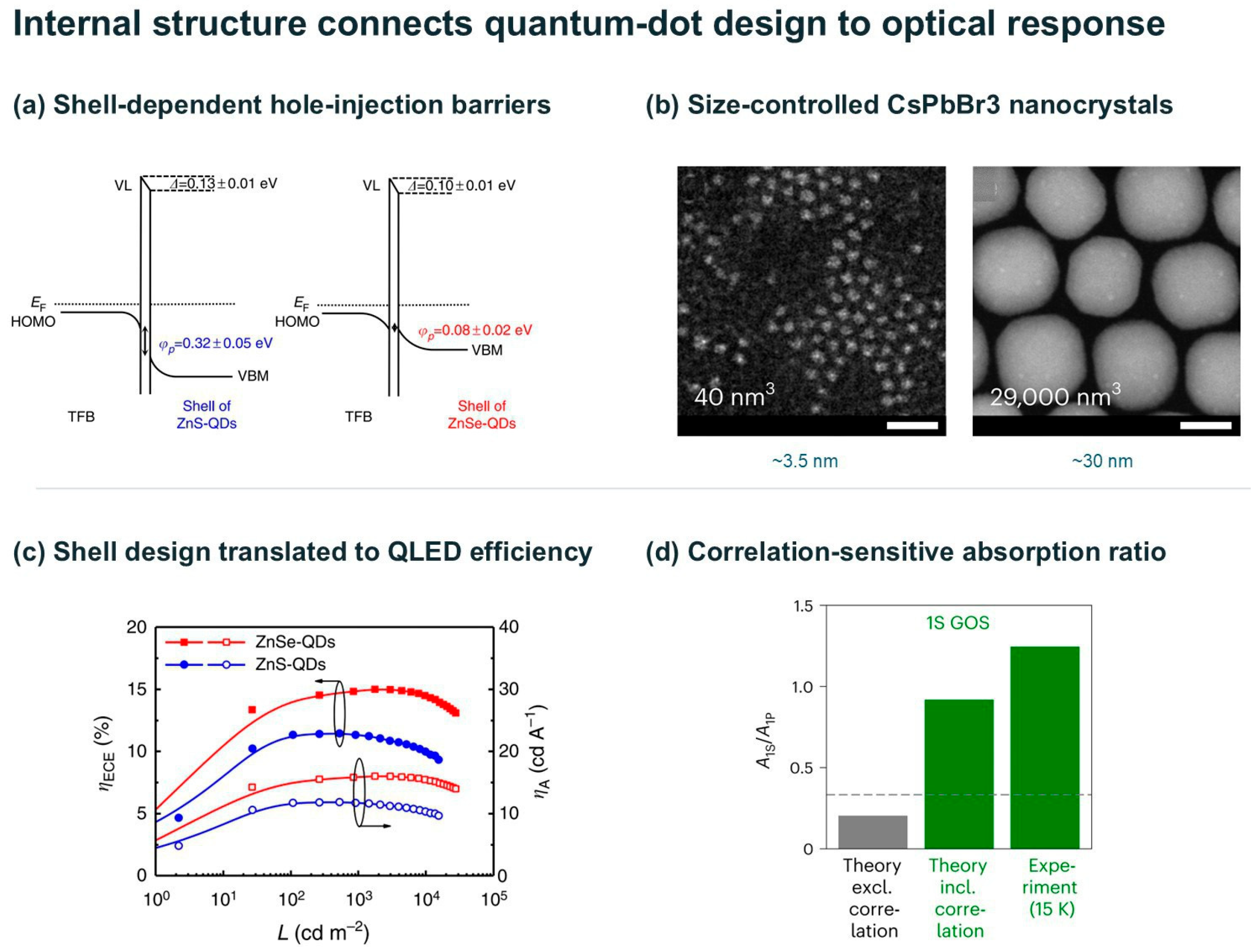
Table 2.
Comparison of major quantum-dot systems for multifunctional optoelectronics. Ratings are qualitative and are assigned from the experimental ranges reported in the cited references, with five filled circles indicating excellent performance and one indicating poor performance. Four filled circles (●●●●) indicate the second-highest rating on the five-point scale for the corresponding criterion. Peak PLQY follows the best reported ensemble values, with five circles for values near unity, three for 40 to 90% and two for families whose typical values stay below 40%. Charge transport follows reported film mobilities and the availability of ligand-exchange routes to conductive films, with five circles for the lead and mercury chalcogenides whose ligand-exchanged films reach the highest reported mobilities [7] and two for families used mainly as dispersed emitters. Environmental compatibility reflects only the regulatory status and documented toxicity of the constituent elements, and precursors, ligands and degradation products are discussed in Section 2.2. Operational stability reflects reported film or device lifetimes under heat, moisture, light and electrical stress. Processability reflects the maturity of solution deposition and patterning. Application maturity reflects the highest readiness level reached, from laboratory demonstrations (two circles) to commercial products (five circles). The Main limitations column names the dominant obstacle reported for each family.
2.5. Unifying Physical Principles and Design Framework
The trade-offs that recur throughout this review can be traced to a small set of physical quantities, and these quantities provide the conceptual framework for Section 3, Section 4, Section 5 and Section 6. Firstly, confinement sets the energy scale. The band-edge transition shifts above the bulk bandgap by a confinement energy that grows approximately as the inverse square of the particle radius in the strong-confinement regime, so composition selects the spectral window and size tunes the position within it, while the same scaling converts a size dispersion into an inhomogeneous linewidth and into the energetic disorder that later limits transport. Secondly, the fate of an exciton is a competition between rates. The radiative rate is set by the oscillator strength and the electron-hole overlap, the trap-assisted rate by the density of surface and interface states, and the Auger rate by the Coulomb coupling of carriers confined in a small volume. Robel et al. found that the biexciton Auger lifetime scales approximately linearly with particle volume across direct-gap and indirect-gap nanocrystals [85], so strong confinement, which favors spectral purity and a high radiative rate, accelerates the very process that causes QLED efficiency roll-off and raises laser gain thresholds. Thick shells, graded interfaces and weak confinement lengthen Auger lifetimes, and the same shells raise injection barriers. Thirdly, transport between dots is tunneling. The electronic coupling between neighbors decays exponentially with the interparticle distance set by the ligand length, and the mobility of a dot solid rises with the square of this coupling until energetic disorder localizes the carriers [86]. Passivating ligands and protective shells therefore raise the PLQY and lower the coupling through the same molecular change, which is the physical origin of the emission-against-transport trade-off.
Fourthly, trapping and release times decide whether a defect acts as a loss, as a gain mechanism or as a memory. In a photoconductor, the gain equals the ratio of the carrier lifetime to the transit time, while the bandwidth is limited by the inverse of that lifetime, so the gain-bandwidth product is fixed by the transit time and a trap that raises the responsivity lengthens the response in the same proportion [87]. Deep or slowly releasing traps that would be defects in a photodiode become the state variables of a photonic synapse (Section 5.1). Fifthly, photon statistics follow the same rate competition in the opposite direction. The zero-delay correlation of a single emitter is approximately the ratio of the biexciton quantum yield to the exciton quantum yield [88], so the fast Auger decay that must be suppressed for lasing is exactly what produces high single-photon purity. These five relations connect the levers of Section 2.1, Section 2.2, Section 2.3 and Section 2.4 to the device requirements of Section 3, Section 4 and Section 5. Composition and size fix the energy scale, the heterostructure sets the exciton rates, the ligands and the assembly set the coupling, and the processing route determines how much disorder and how many traps the device inherits.
Read in this way, the materials, structures, processing and applications of quantum dots form a connected chain. A composition is chosen for the spectral window, an intraparticle structure is chosen to steer the exciton rates toward the target function, a surface chemistry and an assembly route are chosen to set the coupling and the trap density, and the processing route decides whether the resulting film survives patterning, encapsulation and operation. Table 2 reads along this chain, because the rating of a family in one column constrains its options in the others, and Figure 1 maps the same chain from the materials families through the control strategies to the application areas. Section 3 applies the chain to emitters, in which the exciton must be kept inside the particle; Section 4 applies it to absorbers, in which the carriers must leave the particle; and Section 5 applies it to devices that use trapping, photon statistics or mechanical compliance as functions. Section 6 then returns to the links of the chain that remain weakest.
3. Next-Generation Light Emission and Display Technologies
Light emission is among the most mature applications of quantum dots. Narrow emission bands, wavelength tunability and high PLQY support color-conversion displays and provide a basis for direct electroluminescence and stimulated emission. Electroluminescent devices additionally require efficient, balanced carrier injection, while high-resolution displays and lasers impose further constraints on patterning, optical feedback and thermal management. Translating emitter properties into device performance therefore requires coordinated design of quantum-dot structure, interface chemistry and architecture. In the framework of Section 2.5, emitters are the case in which the exciton must stay within one particle, so the intraparticle levers of composition and heterostructure dominate, while the ligand and assembly levers are adjusted only as far as carrier injection requires. This section discusses QLED efficiency and operational stability, patterning for high-resolution displays, and progress toward electrically pumped lasing. Representative structures, processing strategies and performance metrics are summarized in Figure 6 and Table 3.
Figure 6.
Quantum-dot light-emitting devices and display fabrication strategies. (a) Typical QLED architecture and carrier injection and recombination processes, including charge leakage, interface quenching and light extraction. (b) Evolution of EQE in representative red, green and blue QLEDs. (c) Patterning routes for RGB subpixel arrays, with inkjet printing, photolithography and transfer printing placed along an approximate pixel-density axis according to the display formats in which each has been demonstrated.
3.1. Quantum-Dot Light-Emitting Diodes
QLEDs generally comprise electrodes, charge-transport layers and a quantum-dot emissive layer. In common organic-inorganic architectures, organic materials transport holes and ZnO or related oxide nanoparticles transport electrons. Injected carriers recombine in the quantum-dot layer, as shown in Figure 6a. Device EQE depends on carrier confinement in the emissive layer, electron-hole balance, radiative recombination efficiency and optical outcoupling. These factors multiply, because the EQE is the product of the fraction of injected carriers that form excitons in the dots, the fraction of those excitons that recombine radiatively and the fraction of emitted photons that escape the stack [89], so a deficit in any one factor caps the device regardless of the others. The radiative fraction falls at high current density when a dot holds more than one exciton or an extra charge, since the Auger rate then exceeds the radiative rate by the volume scaling described in Section 2.5, and this competition is the microscopic origin of efficiency roll-off. The effective radiative efficiency in a device is influenced by charging, local fields, interface quenching and operating temperature and cannot be replaced directly by solution PLQY. Improving efficiency therefore requires control of both emission properties and device-level electrical and optical losses.
Efficiency enhancement begins with charge balance. Dai et al. inserted an approximately 6 nm polymethyl methacrylate insulating layer between CdSe/CdS quantum dots and ZnO, obtaining deep-red QLEDs with peak EQE of 20.5% and a turn-on voltage of 1.7 V [3]. Regulation of electron injection while preserving emission demonstrated the need to coordinate emissive-layer quality and charge balance. Organic-inorganic transport-layer engineering subsequently enabled high brightness and EQEs of 30.4%, 22.9% and 19.8% for red, green and blue devices, respectively [90]. Deng et al. used hole-transport polymers with low electron affinity and low energetic disorder to suppress electron leakage at organic-inorganic interfaces. Green and blue peak EQEs reached 28.7% and 21.9%, respectively, and the extrapolated green-device T95 was 580,000 h [91]. These results highlight suppression of parasitic recombination beyond the emissive layer. Extrapolated lifetimes must nevertheless be distinguished from directly measured operation times, and they are not equivalent to the results of continuous-stress aging at the intended luminance. Values such as a T95 of 580,000 h or a T50 above 106 h are obtained by accelerated aging at luminances of several thousand cd m−2 and are scaled to 100 or 1000 cd m−2 with the empirical relation L0n × T = constant, in which the acceleration factor n typically lies between 1.5 and 2 for QLEDs. This scaling assumes that one degradation mechanism operates at both high and low drive, which is not guaranteed when ion migration, Joule heating and interface reactions have different current dependences. Jin et al. showed that the extrapolated lifetime is highly sensitive to the initial luminance and to the fitted acceleration factor, so that a 10% overestimate of the initial luminance already overstates the lifetime by about 20% at n ≈ 1.9, and they recommended characterization against a stabilized luminance [92]. Extrapolation models therefore tend to overestimate device longevity, and extrapolated values should be read as upper bounds that await confirmation by long-term tests under real continuous stress. EQEs exceeding 20% and reaching beyond 30% place selected QLEDs at performance levels comparable to phosphorescent OLEDs and support emissive-display applications. Once radiative efficiency is high, leakage, interface recombination and injection balance become especially important. Outcoupling should also be evaluated through dipole orientation, cavity effects and layer optical constants, since it has no universal planar-device value. Materials quality, carrier transport and optical design consequently require joint optimization.
Blue QLEDs impose more stringent requirements on structure and carrier injection than red and green devices. Blue emission requires either small, strongly confined cores or wide-bandgap compositions such as ZnSe and ZnTeSe, for which injection and passivation are challenging. Higher excited-state energies may increase the driving force for selected interface reactions and nonradiative processes, although degradation also depends on carrier distributions, heating and chemical stability. Emission energy alone cannot determine degradation rates. A lifetime gap consequently persists between blue and longer-wavelength devices. Kim et al. introduced HF and ZnCl2 to eliminate stacking faults in ZnSe-based dots and combined this treatment with chloride ligand exchange, obtaining cadmium-free blue emitters with PLQY approaching 100%. A dual emissive layer with a chlorine concentration gradient improved hole transport, illustrating the combined roles of crystal quality, passivation and transport [93]. Zhang et al. inserted a poly(p-phenylene benzobisoxazole) (PBO) antioxidant interlayer between the hole-transport and quantum-dot layers of cadmium-containing CdZnS/ZnS blue QLEDs. Peak EQE reached 23%, and accelerated testing yielded an estimated T50 of approximately 41,000 h at an initial luminance of 100 cd m−2 [94]. Mitigation of oxidative damage to the transport layer thus provides another route to longer operation. Wu et al. used isoelectronic compositional control to prepare uniform ZnSeTeS dots, reporting cadmium-free pure-blue devices with 24.7% EQE, a 17 nm linewidth and an extrapolated T50 of approximately 29,600 h [15]. These results represent a long-lived cadmium-free blue benchmark. Parallel development of green ZnSeTe devices used graded interface potentials to suppress mismatch defects and Auger losses, achieving 21.7% EQE [95]. However, wavelength, luminance, drive conditions and lifetime extrapolation differ between studies. Blue-device development must address color purity, efficiency, stability and high-brightness operation together.
As peak efficiency improves, operational lifetime and the dynamic evolution of interfaces become increasingly important for practical QLEDs. Degradation involves charge accumulation, trap formation, ligand changes and reactions at transport-layer and electrode interfaces. It rarely reflects a single process in the emissive layer. Structural optimization has been linked to improved hole injection and reduced interface charge accumulation [81]. Using charge-modulation electroabsorption and capacitance-voltage measurements, Chen et al. found that excited electrons could cross the type-II quantum-dot/ZnO junction, leading to space-charge accumulation in the electron-transport layer and increasing operating voltage [96]. He et al. further showed that migration of acetate-related species toward the ZnO/Ag cathode region in red QLEDs could reduce excessive electron injection, improve charge balance and limit associated losses [97]. Migration can therefore cause degradation or temporarily improve initial performance, depending on the pathway, reactions and starting injection balance. Stability studies must connect performance evolution with internal changes under actual drive conditions. Figure 7 compares PBO-mediated interface protection with operational interface evolution [94,97]. An initial efficiency increase should be interpreted alongside chemical changes and long-term operation and is not sufficient evidence of improved reliability.
Figure 7.
Interface protection and operational evolution in QLEDs. (a) Simplified active-layer stack of a blue QLED with a 10 nm PBO interlayer. Not to scale. (b) EQE-voltage curves with and without PBO. (c) Normalized operational luminance under the initial luminances and current densities indicated in the plot. (a–c) Adapted under CC BY 4.0 [94]. Copyright 2024, Zhang et al. (d) Relative EL and PL intensities during periodic electrical stressing and scanning at 100 mA cm−2. (e) ToF-SIMS depth profiles across pristine and aged ZnO/Ag interfaces. (f) Proposed pathway linking acetate redistribution, contact deterioration and reduced electron injection to changes in charge balance. (d–f) Adapted under CC BY 4.0 [97]. Copyright 2023, He et al. Efficiency elevation during operation does not by itself establish improved long-term reliability.
3.2. High-Resolution Displays and Microdisplays for AR and VR
Integration of efficient emitters into displays requires accurate positioning, uniform films and reliable subpixel addressing. Augmented-reality and virtual-reality (AR/VR) microdisplays require small pixel pitches, high brightness and consistent color within limited display areas, making patterning a major constraint. Minimum feature size, monochromatic pattern density, full-color pixel density and active-matrix resolution describe different outcomes. Pixels per inch (PPI), dots per inch (dpi) and pixels per degree (PPD) are also distinct. PPD depends on display optics and field of view and cannot be compared directly with PPI. Pixel definitions, spacing and architecture must therefore be specified when assessing the significance of patterning results.
Inkjet printing deposits quantum-dot inks on demand and provides efficient materials use, digital control and compatibility with large-area processing. Droplet size, placement, wetting and drying are the main challenges. Coffee-ring formation and thickness variations can create nonuniform current distributions, affecting efficiency and lifetime. Optimizing solvents, rheology and surface energy has enabled uniform emissive layers and red QLEDs with EQE above 23% [98]. This establishes compatibility between printing and efficient electroluminescence. Further pitch reduction is limited by spreading and crosstalk between neighboring pixels. Suitability depends on display area, target density and throughput as well as on single-device efficiency.
Transfer printing achieves very high pattern densities by separating film formation from patterning. Elastomeric or engineered stamps pick up preformed films and release them onto a target substrate. Nam et al. developed thermodynamically driven immersion transfer using changes in interface adhesion to release and transfer submicrometer RGB patterns. At a two-inch viewing distance, the reported angular resolution was 368 PPD [99]. Combining transfer printing with Langmuir-Blodgett assembly subsequently enabled densities from 9072 to 25,400 PPI. Honeycomb barriers made from wider-bandgap dots reduced leakage between emitting pixels. Red devices reached 262,400 cd m−2 at 8 V and peak EQE of 14.72%, highlighting the importance of interpixel electrical isolation [100]. Yoo et al. engineered viscoelastic stamp surfaces to transfer quantum-dot/ZnO bilayers, obtaining 2565 PPI RGB patterns, approximately 20,526 PPI monochromatic patterns and an EQE of 23.3% [101]. The efficiency improvement was associated with dense particle packing and reduced leakage. Lin et al. combined hard-silicon nanoimprinting with integral inverted transfer through dual-force dynamics, producing RGB arrays from 9072 to 25,400 PPI with transfer yields above 99.9%. The method was demonstrated on rigid and flexible substrates with CdSe/ZnS and perovskite dots [27]. Incorporating TiO2 nanoparticles into the leakage-blocking layer adjusted its dielectric properties and reduced edge-field nonuniformity. An optimized 12,700 PPI red device achieved a peak EQE of 26.1%. Maximum density, efficiency and lifetime refer to different patterns or operating conditions and should not be combined into a single device specification. Scaling still requires improvements in large-area alignment, stamp reuse, defect control, throughput and yield.
Photolithography offers parallel processing and accurate alignment, which make it attractive for integrating quantum-dot pixels with thin-film transistors or CMOS backplanes. Resists, solvents, developers and exposure can, however, change surface coordination and compromise emission or transport. Direct photopatterning uses photoresponsive ligands or crosslinking components to change solubility locally and reduce dependence on conventional resists. Multifunctional ligands combining passivation, photoreactivity and environmental protection have enabled patterning at up to 9534 dpi in air. Corresponding green, blue and red QLEDs achieved EQEs of 25.6%, 21.6% and 20.2% and were integrated with thin-film-transistor backplanes [102]. Exposure dose, residual developer and post-crosslinking transport still require coordinated optimization. For color-conversion microdisplays, Jing et al. integrated lithographically fabricated blue Micro-QLEDs with red and green quantum-dot conversion layers, demonstrating 2 × 2 μm blue electroluminescent pixels and a 1184 PPI full-color prototype [103]. Blue-pixel dimensions do not directly specify full-color pixel pitch, which also depends on subpixel arrangement, spacing and the backplane.
As summarized in Figure 6c, inkjet printing supports on-demand deposition, transfer printing enables fine patterns and heterogeneous integration, and photolithography provides parallel processing and alignment. Practical fabrication may combine these methods. Selection should account for resolution, retained emission, uniformity, area and cost in addition to minimum feature size. Quantum dots also occupy distinct roles in display architectures. In color conversion, a blue source excites patterned red and green layers. The device in Ref. [103] uses blue Micro-QLEDs to convert part of the blue output into red and green light. Overall stability depends on both the excitation device and conversion layers. In directly emissive ultrahigh-resolution QLEDs, the patterned quantum-dot layer itself is electrically driven, simplifying the stack and providing self-emissive contrast but retaining the lifetime constraints of QLEDs, especially in blue [27]. The two approaches therefore have different optimization targets. Figure 8 illustrates fine RGB patterns from immersion transfer and full-color arrays from lithography-assisted integration [99,103]. Pattern resolution, monochromatic efficiency and full-color integration describe different test objects and must be assessed separately.
Figure 8.
Quantum-dot patterning, device performance and full-color integration. (a) Simplified immersion-transfer-printing process. (b) RGB patterns with a feature width of 0.5 μm and an angular resolution of 368 PPD at a two-inch viewing distance. Scale bar, 50 μm. (c) Current efficiency and EQE versus current density for monochromatic immersion-transfer-printed and contact-printed QLEDs. (a–c) Adapted under CC BY 4.0 [99]. Copyright 2020, Nam et al. (d) Electroluminescence image of 2 × 2 μm blue Micro-QLED pixels. Scale bar, 50 μm. (e) Peak EQE versus pixel size. Error bars represent standard deviations from more than six samples. (f) Full-color array with 8 × 8 μm subpixels and red/green quantum-dot color-conversion layers. Scale bar, 100 μm. (d–f) Adapted under CC BY 4.0 [103]. Copyright 2025, Jing et al. The efficiencies in (c) must not be assigned to the highest-resolution pattern in (b). PPD and PPI are distinct quantities.
3.3. Electrically Pumped Quantum-Dot Lasers
Coherent light generation remains one of the most demanding applications of solution-processable quantum dots. The pursuit of laser diodes is constrained by the same confinement physics that supports their emission. Conventional gain in strongly confined dots generally requires multiexciton occupation, but these states often undergo subnanosecond Auger recombination before their energy can be extracted through stimulated emission. Auger losses consequently impose high gain thresholds and short gain lifetimes, making their suppression central to quantum-dot lasing [24]. Because the Auger rate falls with increasing particle volume, the two routes followed below, namely thick or graded shells that enlarge the exciton volume and weakly confined bulk-like particles, are two expressions of one principle, and each buys a longer gain lifetime at the cost of weaker confinement and a smaller spectral shift.
Heterostructure control addresses the gain dynamics directly, because lower gain thresholds and longer gain lifetimes are essential for sustained lasing. Fan et al. used facet-selective epitaxy to grow asymmetric CdS shells around wurtzite CdSe cores. Built-in biaxial strain reduced band-edge degeneracy and the gain threshold while retaining passivation, enabling continuous-wave lasing in colloidal quantum-dot solids [104]. Hahm et al. designed structures combining type-I and type-II characteristics to create hybrid direct/indirect biexcitons with slower, trion-like Auger decay. A static, noncirculating solution in a Littrow cavity produced tunable lasing from 575 to 634 nm, demonstrating that longer gain lifetimes can reduce the concentration required in liquid gain media [105]. Related structures provided gain lifetimes of several nanoseconds and material gain near 1200 cm−1. Modulated laser-diode pumping at duty cycles of 0.1% to 1% enabled quasi-continuous-wave lasing, with thresholds near 500 W cm−2 at 77 K and 3.6 kW cm−2 at room temperature [106]. Weakly confined, bulk-like nanocrystals offer a complementary route. Tanghe et al. reported gain near 50,000 cm−1, an average threshold below one exciton per CdS nanocrystal and a gain lifetime near 3 ns. Bandgap renormalization was proposed to explain these results, which also supported quasi-continuous-wave lasing [107]. In perovskites, matrix and surface engineering improve amplified spontaneous emission (ASE). Zhang et al. added ZrO2 to increase glass-network polymerization and control CsPbBr3 growth. Transient absorption indicated reduced trapping and biexciton Auger recombination, together with faster hot-exciton cooling. The composites achieved an ASE threshold of 54.5 μJ cm−2 under femtosecond excitation and net modal gain of 394.4 cm−1, with greater ASE stability than colloidal controls under the same excitation [60]. Tao et al. instead combined acetate with branched 2-hexyldecanoic acid in the cesium precursor formulation, improving conversion and passivation and reducing the colloidal CsPbBr3 ASE threshold from 1.8 to 0.54 μJ cm−2 [108]. Encapsulation can improve environmental resistance, but refractive index, scattering and thermal transport also influence gain and mode confinement. Threshold and stability must therefore be compared under matched excitation conditions.
The step from optically pumped gain to electrically driven amplification is harder, because optical pumping directly generates electron-hole pairs, whereas electrical operation requires transport through electrodes, transport layers and nanocrystal interfaces. High injection can induce charging, Auger loss and Joule heating. Conductive layers and electrodes also introduce absorption, creating tension between electrical injection and low optical loss. Ahn et al. combined compact graded core/shell dots with a Bragg-reflection waveguide to obtain ASE under pulsed injection at a threshold current density near 13 A cm−2. Dual-band 1S and 1P emission corresponded to gain coefficients of 45 and 55 cm−1 [29]. These results establish that electrically generated gain can overcome device losses, but ASE is not equivalent to laser oscillation with optical feedback. Colloidal processing offers wavelength tunability, substrate flexibility and potentially lower cost. Continuous operation still requires management of the heating and degradation caused by high current densities, as well as absorption in the conductive layers. Stable electrically pumped lasing therefore requires longer gain lifetimes, improved injection, lower optical loss and effective heat removal. Higher material gain or lower transient thresholds alone cannot ensure sustained operation. Auger suppression, carrier balance, feedback and thermal management must be integrated within a common device design.
Table 3.
Representative studies of quantum-dot emission, patterning and optical gain. Lifetimes marked as extrapolated were scaled from accelerated aging at higher luminance with an acceleration factor and are upper estimates (Section 3.1).
4. Photodetection and Energy Harvesting
Tunable absorption and solution processing make quantum dots useful for photodetection and photovoltaics. Unlike emitters, which favor carrier localization and radiative recombination, these devices generally require separation, transport and collection of photogenerated charges before recombination. Ligands, alignment and interparticle coupling can thus adapt one materials family to different functions. In the framework of Section 2.5, absorbers are the case in which carriers must leave the particle, so the interparticle levers of ligand exchange and assembly dominate, and the processing route that sets trap density and disorder decides between gain, speed and noise. The change is not simply a reversal of design targets. Trap-assisted recombination and Auger losses can also restrict detection and photovoltaic performance, while trapping that enhances gain may slow response. This section examines spectral coverage, noise, speed and silicon integration in photodetectors, followed by multiple-exciton generation, solar cells and flexible or semitransparent harvesting architectures. Figure 9 and Table 4 summarize the connections between materials design, carrier dynamics and stability.
Figure 9.
Materials and device design for quantum-dot photodetection and energy harvesting. (a) Representative spectral coverage of quantum-dot photodetector materials from the visible to the long-wave infrared, with the HgSe intraband response distinguished from the interband absorbers. (b) Avalanche photodiode operation, in which a high reverse bias drives impact ionization and carrier multiplication in a dedicated multiplication region. (c) Tandem solar cells, multiple-exciton generation and semitransparent or flexible photovoltaic windows.
4.1. Broadband Photodetectors
A distinctive advantage of colloidal quantum dots is the combination of size-tunable spectral response and direct integration on silicon. Lead and mercury chalcogenide families collectively cover wavelengths from the visible to the very-long-wave infrared through size and compositional control. Solution deposition onto CMOS readout circuits can avoid the indium-bump hybridization used for epitaxial InGaAs and HgCdTe focal-plane arrays, an important contributor to their cost [7]. Figure 9a summarizes the broad spectral coverage.
In the short-wave infrared, PbS dots are the established absorbers for detection near 1 to 2 μm. Increasing size reduces the bandgap but generally makes passivation and dark-current control more difficult, requiring a balance between absorption, collection and noise. Vafaie et al. increased bromide content during halide exchange and introduced secondary passivation for PbS dots with a bandgap near 0.8 eV. The photodiodes achieved approximately 80% EQE and specific detectivity of 8 × 10¹¹ Jones at 1550 nm. Under zero applied bias and pulsed 850 nm excitation, measurements across different pixel sizes yielded a fastest fall time of 10 ns [82]. Improved facet passivation and reduced organic residues can therefore support efficient collection and rapid response. Monolithic PbS integration onto CMOS readout circuits has also produced an imager operating from 400 to 1300 nm, with room-temperature detectivity of 2.1 × 10¹² Jones, a −3 dB bandwidth of 140 kHz and a linear dynamic range above 100 dB [12]. This demonstrates compatibility between film processing, readout integration and imaging. Trapping can provide high gain in phototransistors and photoconductors but often prolongs response or introduces memory. Photodiodes generally offer lower gain but can improve speed, linearity and noise control [7]. The responsivity R is the photocurrent per unit optical power and equals the product of the external quantum efficiency, the elementary charge divided by the photon energy and the photoconductive gain, while the specific detectivity D* normalizes R to the noise current per unit bandwidth and to the device area. A trap that lengthens the carrier lifetime raises the gain and therefore R, but it also raises the generation-recombination noise and lowers the bandwidth, so D* and speed improve only when the noise falls faster than the gain rises, which is why the fast photodiodes above rely on passivation and the high-gain phototransistors of Section 5.1 rely on controlled trapping. Focal-plane evaluation must additionally consider dark-current density, uniformity, defective-pixel fraction and corrected image quality. Peak responsivity or detectivity alone is therefore insufficient for ranking architectures.
Mercury chalcogenide dots extend solution-processed detection into the mid-wave and long-wave infrared through control of size, doping and energy levels. Xue et al. used regrowth and ionic doping to develop HgTe photoconductors with response extending to 18 μm. At liquid-nitrogen temperature, responsivity at 18 μm reached 0.3 A W−1 and detectivity was 6.6 × 10⁸ Jones [83]. HgSe devices provide a complementary intraband route. Mixed-phase ligand exchange and controlled doping improved transport, while 1Se→1Pe conduction-band transitions enabled mid-infrared detection [109]. Device geometry also governs dark current. Huang et al. stacked HgTe and ZnO quantum-dot layers vertically into a heterojunction photovoltaic detector, which lowered the dark current density to 5.23 × 10⁻⁹ A cm−2 at 80 K while retaining a high rectification ratio, and the vertical geometry suits integration on silicon readout circuits [110]. Tang et al. vertically stacked two back-to-back rectifying junctions and switched between SWIR and MWIR response by changing bias polarity and magnitude. Switching modulation reached 100 kHz, and low-temperature detectivity exceeded 1010 Jones [111]. Mu et al. optimized the graded bandgap of PbS/HgTe stacks to obtain response from 0.4 to 5.0 μm and demonstrated a 640 × 512 focal-plane array [13]. To reduce cooling requirements, Caillas et al. integrated gold nanoantennas with HgTe films in a metal-insulator-metal structure. Uncooled photoconductors reached 0.6 A W−1 at 1 V and peak detectivity of 9 × 10⁹ Jones at 2650 cm−1 and 80 kHz, approximately 15 times the value of comparable films without the structure [112]. Optical-field enhancement can thus improve thin-film absorption, although measurement frequency and other conditions remain essential to performance interpretation. Lead and mercury safety, surface stability and array uniformity must also be addressed through encapsulation and manufacturing control.
Sensitivity to weak light can be raised by avalanche multiplication, which supplies internal gain, but high multiplication or detectivity does not by itself establish single-photon counting. Kim et al. applied strong fields across colloidal quantum-dot layers thicker than 540 nm, enabling electrons to acquire sufficient energy for impact ionization. An interdot spacing near 4.1 nm balanced ionization with hopping transport. Optimized devices reached a maximum multiplication gain of 85 and peak detectivity of 1.4 × 10¹⁴ Jones at 940 nm [113]. These results show that transport distance and carrier-energy accumulation can be engineered to achieve avalanche multiplication in solution-processed infrared devices.
Infrared materials with reduced dependence on lead and mercury are also advancing. Wang et al. developed Ag2Te colloidal quantum dots and RoHS-compliant detector stacks with response from 350 to 1600 nm, room-temperature detectivity near 1012 Jones, a −3 dB bandwidth above 0.1 MHz and a linear dynamic range above 118 dB. A monolithically integrated SWIR imager was also demonstrated [30]. Alternative compositions can therefore combine sensitivity, speed and silicon integration. Absence of lead or mercury does not establish negligible toxicity or environmental impact. Silver-ion release, precursors, ligands, degradation products and the full device lifecycle still require evaluation. These newer systems do not yet match all aspects of PbS or HgTe efficiency and spectral coverage. Peng et al. reviewed II-VI, IV-VI, III-V and environmentally preferable systems across photoconductors, phototransistors and photodiodes, reporting detectivities spanning 1010 to 1018 Jones and responses reaching nanosecond timescales [7]. Such comparisons support application-specific selection for imaging, wearable monitoring and artificial vision.
Group IV nanostructures provide a silicon-compatible route to near-infrared detection that avoids lead, mercury and indium altogether. Ge quantum dots grown on silicon by Stranski-Krastanov epitaxy absorb beyond the silicon band edge, and p-i-n photodiodes with multilayer Ge/Si dot stacks were demonstrated for the 1.3 to 1.5 μm telecommunication window two decades ago, although a quantum efficiency of about 3% at 1.3 μm reflected the small absorbing volume of the dot layers [42]. Light management has since compensated for this limitation. Microstructured hole arrays etched into Ge/Si quantum-dot photodiodes raised the normal-incidence responsivity resonantly by factors of 40, 33 and 30 at 1.4, 1.7 and 1.9 μm relative to an unpatterned reference, and the response could be tuned through the angle of incidence [84]. Beyond quantum-dot architectures, GeSn alloy photodetectors provide another route to silicon-compatible infrared detection. For example, Ge0.955Sn0.045 pn photodetectors prepared by ion-beam synthesis have achieved a responsivity of 0.56 A W−1 at 1.71 μm at room temperature, with a dark current density of 12.8 mA cm−2 [114]. Colloidal Ge1−xSnx dots extend this composition control to solution processing, with absorption onsets tunable from 1.72 to 0.84 eV as the tin fraction rises to 20.6% [48]. Group IV detectors trade the broad spectral reach and high gain of the mercury chalcogenides for monolithic fabrication in CMOS foundries and benign chemistry, and the open questions are the low absorption coefficient of indirect-gap dots, the dark current of defective Ge/Si interfaces and the stability of tin-rich alloys [69].
4.2. Quantum-Dot Photovoltaics and Multifunctional Energy Harvesting
Tunable bandgaps, low-temperature processing and structural flexibility motivate quantum-dot photovoltaics. Their value relative to established solar cells depends not only on single-junction power conversion efficiency but also on infrared utilization, tandem compatibility and flexible or semitransparent form factors. Evaluation must connect charge generation, film transport and the intended application to identify the specific benefit of quantum dots.
Multiple-exciton generation (MEG) converts one absorbed high-energy photon into two or more electron-hole pairs. Recovering energy otherwise lost through thermalization can, in principle, raise photovoltaic efficiency beyond the conventional Shockley-Queisser limit. Confinement can promote carrier multiplication by modifying cooling and carrier interactions. The process is Auger recombination run in reverse, since a hot carrier with excess energy above the bandgap gives that energy to a second electron-hole pair instead of releasing it as phonons, so the same Coulomb coupling that limits emitters becomes a resource for absorbers. Semonin et al. measured peak EQE of (114 ± 1)% in PbSe quantum-dot solar cells and an internal quantum efficiency of 130% after correcting for reflection and absorption losses. Comparison with transient absorption in isolated dots supported collection of the additional carriers by the external circuit [115]. Davis et al. subsequently achieved peak EQE above 120% in PbSe nanorod cells, providing a basis for examining morphology-dependent multiplication [116]. MEG devices must nevertheless suppress multicarrier recombination and support extraction. MEG remains primarily a demonstration of principle rather than an established deployment-level efficiency benefit, but it offers a long-term route beyond conventional thermalization-limited photovoltaics.
For single-junction solar cells, CsPbI3 and PbS are the most important quantum-dot absorbers. In CsPbI3, nanoscale surface energy and ligands help stabilize the photoactive phase, although stability also depends on size, composition and the environment and cannot be attributed solely to confinement. Early α-CsPbI3 cells combined phase stabilization with improved interdot transport [117,118]. Jia et al. added KOH to methyl benzoate antisolvent to promote hydrolysis and replace surface oleate with shorter benzoate ligands. Mixed-A-site perovskite quantum-dot devices achieved 18.37% power conversion efficiency (PCE), with a certified value of 18.30% [28]. This supports improved extraction while retaining ligand coverage. PbS cells reached 13.8% PCE using a monolayer perovskite bridge that doubled the carrier diffusion length [119]. These examples identify interdot transport as a major limitation and highlight interfaces that improve coupling without restoring traps. Wang et al. used cation disorder to enhance AgBiS2 absorption, obtaining 9.17% PCE, certified at 8.85%, with an absorber only 30 nm thick [72]. Control of cation arrangement thus provides a route to ultrathin absorbers without lead or cadmium.
Beyond single junctions, quantum-dot photovoltaics offer spectral complementarity for tandems and adaptable form factors for flexible and transparent devices. Tandem subcells require matched bandgaps and absorption ranges. Narrow-bandgap infrared dots can harvest low-energy photons transmitted by an upper cell, while the role of perovskite dots depends on composition, bandgap and position. Alignment, interface recombination and extraction jointly determine performance. Hu et al. incorporated PCBM into CsPbI3 layers to combine charge transfer with interface adhesion, obtaining flexible cells with 12.3% PCE on PET/ITO. After 100 bending cycles at a radius of 0.75 cm, quantum-dot devices retained approximately 90% of their initial efficiency, compared with approximately 75% for CsPbI2Br thin-film controls [77]. Mechanical accommodation and interface engineering therefore both contribute to flexible performance. Luminescent solar concentrators (LSCs) employ a different approach. Quantum dots in a transparent plate absorb sunlight and guide re-emitted light to cells at the edges. Bergren et al. embedded near-infrared-emitting CuInS2/ZnS dots in a polymer interlayer between low-iron float-glass sheets, producing a 10 cm × 10 cm LSC with 8.1% optical efficiency at approximately 44% visible transmittance. With perimeter silicon cells, certified PCEs were 2.2% with a black background and 2.9% with a reflective backing [73]. This demonstrates integrated transmission, optical concentration and edge-mounted power generation.
A central photovoltaic trade-off concerns the coupling required for extraction and the long-term stability of the resulting films. Extensive ligand exchange and conductive terminations can expose dots to oxidation and ionic redistribution under prolonged illumination, thermal cycling and humidity. Perovskite-dot cells also retain moisture sensitivity and phase-stability constraints. Reported efficiencies are commonly initial or best-device values measured under controlled conditions. Certified, stabilized efficiencies established through standardized aging remain less common. The difference between initial performance and sustained output is therefore critical to deployment readiness.
Table 4.
Representative studies of quantum-dot photodetection and energy harvesting.
5. Interdisciplinary and Emerging Optoelectronics
Beyond displays, photodetection and energy harvesting, quantum dots are increasingly investigated for neuromorphic computing, quantum information and flexible or biointegrated optoelectronics. These applications combine functions such as photoresponse and charge memory, exciton control and single-photon emission, or spectral tunability and mechanical compliance. Performance depends on coordination between physical processes and system requirements, and no single metric such as efficiency or responsivity captures it. A property can also have different consequences across applications. Trapping restricts fast detection but enables synaptic memory. Auger recombination suppresses multiexciton gain but can reduce multiphoton emission under suitable conditions. The applications in this section use the rate competitions of Section 2.5 as functions, since trapping times become memory, Auger decay becomes photon purity, and the assembly becomes a mechanical as well as an electronic design variable. This section examines representative advances and the challenges of moving from individual devices to integrated systems, as summarized in Figure 10 and Table 5.
Figure 10.
Interdisciplinary and emerging applications of quantum dots. (a) Charge trapping and release in a quantum-dot phototransistor under an optical spike train, with paired-pulse facilitation leading to long-term potentiation. (b) Antibunched single-photon emission from an optically pumped dot, with g(2)(0) near zero as the purity metric. (c) A stretchable QLED on skin under uniaxial strain. (d) Near-infrared fluorescence imaging through tissue and quantum-dot photovoltaic neural stimulation.
5.1. Photonic Synapses and Neuromorphic Computing
Data transfer between memory and processing units introduces energy costs and latency in conventional computing. Vision systems additionally require pixel readout, conversion and transmission before processing. Introducing preprocessing and memory at the sensing stage can reduce redundant transfer. Photonic synapses convert optical inputs into electrical responses that depend on stimulation history, providing a basis for combining sensing, storage and computation. In quantum-dot devices, photogenerated carriers can become trapped in dots or heterointerfaces and modulate a conductive channel through photogating or changes in interface potential. Slow release produces a decaying current after illumination ends. Trap energies, interface coupling and pulse conditions regulate response amplitude and retention, allowing paired-pulse facilitation and short-term or long-term potentiation to be reproduced. The retention time follows from the trap depth, because thermal release is exponentially slower for deeper states, and the probability of filling a trap during a light pulse follows from the tunneling barrier between the channel and the dot. Wen et al. demonstrated this control directly in InP/ZnSe core/shell dots, in which the thickness of the ZnSe shell set the charge storability of the transistor memory, so the device with the thickest shell reproduced paired-pulse facilitation, short-term and long-term memory and experience-dependent learning under optical programming and electrical erasing, while a positive gate bias strengthened the optical response [120]. Composition and size additionally enable wavelength-selective inputs.
Research has expanded from single-device memory toward coordinated sensing, preprocessing and recognition. Pradhan et al. grew MAPbBr3 dots directly at graphene defect sites, combining photogeneration and transport in a hybrid structure. The phototransistors achieved responsivity of 1.4 × 10⁸ A W−1 at 430 nm and detectivity of 4.72 × 10¹⁵ Jones. Gate control enabled retained photoconductance and synaptic plasticity, which were used in machine-learning-assisted face-recognition studies. Interface transfer and photogating thus supported both high-gain detection and optical memory [16]. Integration of synaptic phototransistors with QLEDs further combined accumulated responses to repeated optical stimuli with threshold emission, enabling noise suppression and visualization of ultraviolet patterns before recognition [121]. Gupta et al. introduced a CsPbBr3 charge-trapping layer into P3HT-channel transistors, using spatial charge separation to obtain nonvolatile memory, paired-pulse facilitation, short-term and long-term plasticity, and a dynamic range near 103. Neural-network simulations based on measured weight updates achieved approximately 85% pattern-recognition accuracy after 120 training epochs [122]. All-inorganic CsPbBr3 devices also combined sensing and synaptic response, using wavelength-dependent weight changes in simulations of colored handwritten-digit recognition [123]. These results demonstrate ways to use spectral information near the sensor.
Materials selection and interface engineering are extending photonic synapses toward cadmium-free and lead-free systems and flexible architectures. Luo et al. used Cu doping in inverted type-I ZnSe/InP dots to extend response into the near-infrared. The devices reproduced short-term and long-term plasticity and learning, forgetting and relearning under near-infrared stimulation [124]. In a different architecture, CuInGaSe/ZnSe photoelectrochemical synapses responded to optical pulses in aqueous electrolytes, exhibiting paired-pulse facilitation and short-term and long-term plasticity [125]. Lu et al. exchanged InP surface ligands with fluorinated thiols to improve photostability and alignment with an organic semiconductor. Long charge retention was associated with ligand-induced interface dipoles. Flexible transistors reproduced corneal nociceptor behavior and used color selectivity to extract blue features while suppressing red and green backgrounds [126]. Perovskite-dot/IGZO hybrid transistors additionally tuned their detection band through Cl/Br composition while retaining paired-pulse facilitation, long-term memory and gate-controlled erasure [127]. These studies exploit energy levels, ligands, operating media and halide composition, but device plasticity, simulated network performance and complete hardware capabilities must be evaluated separately.
Retinomorphic sensing and reservoir computing are two promising extensions. Retinomorphic arrays use spatial and temporal response to perform edge enhancement, motion detection or adaptation before readout. Reservoir computing exploits nonlinearity and fading memory to map temporal inputs into dynamic states that are interpreted by a readout layer. Traps and interface dynamics provide physical states, but input encoding, driving, readout and training still consume energy. Natural device evolution should not be equated with energy-free computation. Both architectures require traps to become controlled design variables. Appropriate trapping supports memory, whereas deep or broadly distributed traps can impede reset and cause drift or variability. Defect engineering therefore concerns energy, density, position and trapping and release timescales, and increasing trap numbers alone does not help. Evaluation must distinguish individual synaptic properties, software simulations based on measured parameters and tasks executed by hardware arrays. Recognition accuracy depends on dataset size, training, peripheral circuitry and energy accounting and is not a universal device metric. Uniformity, addressability, retention, endurance and the combined energy of optical input and electrical reset remain integration challenges. Standardized tasks and complete system tests are needed to establish where quantum-dot synapses offer practical advantages.
5.2. Quantum Information and Single-Photon Sources
Quantum-dot light sources seek to combine single-photon purity, brightness and indistinguishability for quantum communication, photonic computing and sensing. Somaschi et al. integrated epitaxial dots into electrically controlled cavities and suppressed charge noise through biasing. Under resonant excitation, photon indistinguishability reached 0.9956 ± 0.0045 and the zero-delay second-order correlation was g(2)(0) = 0.0028 ± 0.0012, establishing a benchmark for high-purity, highly indistinguishable solid-state emission [44]. Colloidal and perovskite dots offer solution processing, compositional and size control, and modifiable surfaces for room-temperature emission and integration. Their development must address coherence, stability and deterministic positioning, as well as multiphoton suppression [11].
Confinement and Auger recombination can regulate multiexciton emission, but their effects depend on excitation and recombination dynamics. When nonradiative biexciton decay dominates radiative decay, multiphoton emission can be suppressed and antibunching improved. Quantitatively, the zero-delay correlation of a single dot approximates the ratio of the biexciton quantum yield to the exciton quantum yield [88], so a small particle with fast Auger decay is a purer single-photon source and a poorer gain medium at the same time, which is the inverse of the requirement in Section 3.3. Zhu et al. compared perovskite dots of different sizes and compositions and obtained a minimum g(2)(0) near 0.02 from individual CsPbI3 dots with a mean edge length near 6.6 nm. The measurements used nonresonant excitation at room temperature without a cavity and corresponded to the reported single-photon purity of approximately 98% [17]. High purity does not automatically imply indistinguishability. Blinking, spectral diffusion and phonon coupling require separate control. Mi et al. promoted π-π stacking between phenethylammonium ligand tails to stabilize CsPbBr3 surfaces. Nearly nonblinking emission and approximately 98% purity were obtained, with representative particles remaining stable after 12 h of continuous excitation [76]. Open-microcavity integration provides another route, narrowing room-temperature output to approximately 1 nm while retaining 94% single-photon purity under pulsed and continuous-wave excitation [128]. Lin et al. sparsely embedded isolated CdSe/CdS core/shell dots in an insulating layer between electron- and hole-transport layers. Room-temperature electrical excitation yielded g(2)(0) = 0.045 ± 0.005 without spectral filtering or background correction [18]. Exciton fine structure can also control other photon statistics. Tamarat et al. found that the long-lived dark-exciton ground state of CsPbI3 nanocrystals promoted biexciton formation and correlated photon-pair emission at low temperature. Magnetic field or temperature tuning enabled transitions between bunching and antibunching [129]. Boehme et al. observed increasing low-temperature band-edge absorption with particle volume in large CsPbBr3 dots and used configuration-interaction calculations to attribute single-photon superabsorption to intraparticle electron-hole pair correlations [80]. These results extend photon-statistics control and light-matter coupling through distinct mechanisms. Figure 11 contrasts room-temperature electrical single-photon emission enabled by isolation [18] with low-temperature bunching and cascade emission influenced by dark excitons [129]. The materials, excitation conditions and target statistics differ. Correlated photon-pair emission alone does not establish entanglement.
Figure 11.
Control of quantum-dot photon statistics by electrical isolation and dark-exciton dynamics. (a) Simplified active region of an isolated CdSe/CdS quantum-dot device. (b) Voltage-dependent integrated electroluminescence of quantum dots and Poly-TPD with 12 nm PMMA over the same 1-mm2 emitting area. (c) Room-temperature electroluminescence correlation at 2.6 V, with g(2)(0) = 0.045 ± 0.005 without spectral filtering or background correction. (a to c) Adapted under CC BY 4.0 [18]. Copyright 2017, Lin et al. (d) Qualitative four-level pathway for dark-state shelving and biexciton-bright-exciton cascades in CsPbI3. Not to scale. (e) Photon-coincidence histograms at 4 K under 0, 2 and 7 T. (f) XX-X cross-correlation (left) and exciton-filtered X-X autocorrelation (right) for the same nanocrystal at 4 K and zero field. The vertical scales differ. (d–f) Adapted under CC BY 4.0 [129]. Copyright 2020, Tamarat et al. G, X and XX denote ground, exciton and biexciton states. The rows represent different materials and excitation conditions.
For integration, colloidal dots could be positioned, patterned or transferred onto waveguides and microcavities, including silicon nitride structures, to combine sources, modulation and detection on a chip. Processability is an advantage, but positioning accuracy, dipole orientation, coupling and post-fabrication surface stability remain challenges. Epitaxial dots can also enter such structures through heterogeneous integration, so approaches should be compared through manufacturing complexity and final optical performance. Quantum-dot spin states and spin-photon coupling provide another direction, using optical transitions to initialize, manipulate and read electron or hole spins [11]. These functions impose additional requirements on local environments, coherence and charge-state stability and should be distinguished from established single-photon demonstrations. A low g(2)(0) indicates suppressed multiphoton events but does not establish high indistinguishability. Room-temperature phonons, pure dephasing and spectral diffusion may still broaden emission beyond the transform limit. Colloidal platforms nevertheless offer room-temperature operation, electrical excitation, visible-to-near-infrared tunability and compatibility with silicon photonics through direct deposition. For selected quantum-key-distribution and sensing applications, brightness, cost and integration can be more decisive than high indistinguishability, providing a differentiated role for colloidal sources.
5.3. Flexible and Biointegrated Optoelectronics
Low-temperature processing, modifiable surfaces and tunable spectra enable quantum dots to be combined with flexible substrates, elastomers and biological interfaces. Nanoparticles alone do not determine the flexibility or biological compatibility of a complete device. Mechanical behavior depends on the functional layers and interfaces, while biological outcomes depend on composition, size, coating, dose and exposure route.
Stretchable and skin-mounted emitters must retain mechanical compliance, interparticle coupling and transport. Kim et al. blended colloidal dots, an elastomer and a charge-transport polymer into a ternary emissive nanocomposite. Interparticle spacing remained nearly constant at 50% strain, while a polymer-rich bottom region supported hole transport. The intrinsically stretchable QLEDs had a turn-on voltage of 3.2 V and reached 15,170 cd m−2 at 6.2 V without luminance loss at 50% strain [8]. Local particle organization and transport-network design thus mitigated deformation-induced changes. Complementary photoluminescent conversion layers can be optically integrated with micro-LEDs. Crosslinking has enabled uniform, concentrated quantum-dot dispersions in polydimethylsiloxane, maintaining low backlight leakage at 50% strain and supporting pattern densities up to 300 PPI. Demonstrations included robotic skin and wearable monitoring [130]. Both approaches show that stretchable performance depends jointly on emitters, polymer networks and architecture.
For biointegrated imaging, sensing and neural interfaces, tunable near-infrared emission can reduce tissue scattering and autofluorescence, although imaging also depends on wavelength-dependent water absorption, probe brightness and detection conditions. Bruns et al. engineered InAs-based core/shell dots and surface functionalization for SWIR imaging in mice. Quantum-dot-labeled lipoproteins enabled tracking between blood, brown adipose tissue and liver, supporting real-time quantitative analysis of metabolism [20]. Zhang et al. protected approximately 1600 nm-emitting PbS cores with CdS shells and retained fluorescence after aqueous transfer through polymer coating and PEG modification. Under 808 nm excitation, NIR-IIb imaging used exposure times as short as 2 to 5 ms and enabled blood-flow observation at 60 frames s−1 [21]. Near-infrared absorption can also drive photoelectrical neural interfaces. Karatum et al. integrated PbS dots with ZnO, P3HT and a RuO2 return electrode, generating capacitive interface responses under 780 nm illumination and inducing action potentials in cultured hippocampal neurons without genetic modification [19]. Long-chain dithiol ligands have also enabled low-dose near-infrared detection and image communication in PbS/IGZO phototransistors [131]. Yu et al. connected an organic bulk-heterojunction photodetector with a ZnSe/ZnS emitter through Mg-doped ZnO, improving transport and reducing interface losses. Near-infrared-to-blue photon conversion increased from 2.91% to 8.68%, with flexible devices demonstrated for heart-rate measurement and biological-tissue microscopy [132]. Carbon and biomolecule-derived dots offer complementary candidates that reduce dependence on cadmium and lead, using renewable precursors and modifiable surfaces for biosensing [9,10].
Biointegrated devices may require flexibility, biological compatibility, spectral matching to tissue windows and stability in warm, ion-rich aqueous environments. These requirements vary with use. In vivo probes emphasize biodistribution and clearance, skin-mounted devices require mechanical matching and prolonged-contact compatibility, and implanted neural interfaces demand stable electrochemistry and tissue compatibility. Quantum-dot multifunctionality provides design freedom, but reliable application depends on meeting the specific optical, electrical, mechanical and biological requirements together.
Table 5.
Representative quantum-dot devices for interdisciplinary and emerging optoelectronics.
6. Challenges and Future Perspectives
Progress in emission, detection and emerging optoelectronics demonstrates the potential of quantum dots as multifunctional materials, but translation into applications requires reconciliation of performance, environmental compatibility and long-term reliability. Some high-performance systems contain cadmium, lead or mercury, and degradation and ion release can affect both lifetime and environmental risk [55,57,58]. Materials selection should therefore reflect use conditions. Core/shell protection, barrier encapsulation and recycling can reduce exposure from sealed devices, whereas biointegrated or environmentally exposed applications motivate alternatives with fewer hazardous constituents. InP, Ag2Te, AgBiS2, copper halides and group IV dots provide different options. Cadmium-free or lead-free composition does not automatically establish low toxicity or sustainability. Precursors, synthesis energy, degradation products and lifecycle impacts require evaluation [30,52,53,54,56,61,72]. Two examples show what this direction already delivers. The Ag2Te image sensor of Wang et al. reaches a detectivity near 1012 Jones at room temperature in a RoHS-compliant stack and is integrated monolithically on a silicon readout circuit, which shows that lead-free and mercury-free infrared imaging is attainable, while its silver-ion release and precursor burden remain to be assessed [30]. The Eu3+-doped CsMnBr3 glass of Ye et al. retains its red emission for more than 450 days and operates in prototype LEDs, which shows how encapsulation in an inorganic matrix can make a lead-free emitter stable enough for lighting [66]. Future optimization should consider these factors alongside emission, transport and spectral properties.
Operational stability and scalable manufacturing are interconnected challenges. Ion migration, ligand changes, interface reactions and local heating can couple within devices, making initial performance an unreliable predictor of sustained output [29,81,96,97]. In situ measurements should identify dominant failure pathways and guide ligand stabilization, interface barriers, injection balance and thermal management. Scaling small devices to large films and wafer-scale arrays also requires stable inks, uniform drying, multilayer alignment and consistent pixels. Printing and direct CMOS integration provide a foundation, but process-specific thermal budgets, solvent compatibility and contamination must be controlled, and yield and batch reproducibility must be demonstrated [7,12,98]. Two examples mark the current frontier. The monolithic PbS imager of Liu et al. operates from 400 to 1300 nm on a silicon readout circuit and the PbS/HgTe stack of Mu et al. forms a 640 × 512 focal-plane array, so wafer-level integration has been demonstrated, and the open questions are the pixel-to-pixel uniformity and the long-term dark-current drift of such arrays [12,13]. In displays, the nanoimprint-assisted transfer printing of Lin et al. reaches 25,400 pixels per inch with transfer yields above 99.9% [27], which moves the bottleneck from patterning resolution to the operational lifetime of the patterned blue pixels discussed in Section 3.1. Materials chemistry, device physics and fabrication should therefore develop together so that particle-level advantages translate reproducibly into system performance.
Three materials-level directions named in the Abstract have concrete starting points. For stable blue emitters, the ZnSeTeS dots of Wu et al. combine 24.7% EQE, a 17 nm linewidth and an extrapolated T50 near 29,600 h [15], and the antioxidant PBO interlayer of Zhang et al. raises the estimated T50 of cadmium-containing blue devices to about 41,000 h [94], so the next step is to confirm these extrapolations under continuous stress and to transfer the interface protection to cadmium-free stacks. For electrically pumped lasing, the electrically driven amplified spontaneous emission of Ahn et al. at 13 A cm−2 [29] and the quasi-continuous-wave lasing of Hahm et al. under modulated optical pumping [106] bracket the remaining gap, which is a low-loss resonator that tolerates the current densities and the heating of electrical injection. For room-temperature quantum light sources, the electrically driven CdSe/CdS device of Lin et al. with g(2)(0) of 0.045 [18] and the nonblinking CsPbBr3 dots of Mi et al. with 12 h of stable emission [76] show that purity and stability can be reached separately, and the direction is to reach both in one emitter coupled to a cavity, as the microcavity-narrowed perovskite source of Farrow et al. begins to do [128].
The system-level directions are at an earlier stage. For in-sensor visual computing, the perovskite-on-graphene phototransistors of Pradhan et al. perform face recognition with machine-learning assistance [16], the fluorinated InP synapses of Lu et al. extract blue features from a colored scene on a flexible substrate [126], and the InP/ZnSe devices of Wen et al. show that the shell thickness can serve as a design rule for retention [120]. The step from these demonstrations to hardware arrays requires uniform devices, addressable erasure and an energy accounting that includes the optical input. For implantable photonic biointerfaces, the PbS photovoltaic interface of Karatum et al. evokes action potentials in hippocampal neurons under 780 nm light without genetic modification [19], and the NIR-to-blue up-conversion device of Yu et al. measures heart rate and images tissue on a flexible substrate [132]. Chronic implantation adds the requirements of long-term stability in warm electrolyte and of a composition without lead, which points back to the environmentally benign emitters above.
Artificial intelligence and automated experiments provide tools for exploring this multiobjective design space. Machine-learning-guided synthesis and autonomous platforms have optimized composition, size distributions and optical properties while improving screening efficiency [35,36,37,38,39,40]. The Artificial Chemist of Epps et al. optimizes the emission of perovskite dots autonomously in a flow reactor [35], the Smart Dope platform of Bateni et al. extends this approach to doped perovskite dots [38], and Guo et al. used machine learning to realize full-color carbon dots with high quantum yield from a large synthesis space [39]. The next step is to extend targets from initial colloidal optics to complete-device efficiency, noise, lifetime and environmental performance. Physical understanding is needed to improve interpretability and transfer between systems. Reliable data are essential. PLQY, detectivity, lifetime and neuromorphic results should specify conditions, distributions and evaluation methods, with reproducibility and failure data reported alongside favorable outcomes. Research should increasingly optimize coupled functions and their costs rather than individual maxima. Standardized characterization, mechanistic studies and closed-loop experimentation can support stable, manufacturable and sustainable quantum-dot optoelectronics.
7. Conclusions
Quantum dots have evolved from model systems for quantum confinement into multifunctional platforms spanning displays, photodetection, energy harvesting, information processing and biological interfaces. This review connects composition, surface chemistry and heterostructure design with shared control strategies across applications. These relationships expose trade-offs between radiative recombination and transport, confinement and multiexciton dynamics, and performance and environmental compatibility. Section 2.5 condensed these relationships into five physical relations that connect synthesis, structure, surface chemistry and assembly to the requirements of each device class. Application potential depends not only on tunable spectra and solution processing but also on converting these properties into stable device functions. Future work should coordinate materials, interfaces and architectures to address blue-emitter stability, electrically pumped lasing, wafer-scale integration and coherence in room-temperature quantum sources. Environmental assessment and scalable manufacturing must be included in this process. Standardized measurements, in situ mechanistic studies and multiobjective optimization assisted by artificial intelligence can clarify functional trade-offs and accelerate the transition from high-performance demonstrations to reliable and sustainable technologies.
Author Contributions
Conceptualization, X.Z.; methodology, X.Z.; software, Z.L. and S.L.; validation, Z.L. and Y.Y.; investigation, X.Z., S.L. and Y.Y.; writing—original draft preparation, X.Z.; writing—review and editing, X.Z. and X.S.; visualization, X.Z. and S.L.; project administration, X.S.; funding acquisition, X.S. All authors have read and agreed to the published version of the manuscript.
Funding
This work was supported by the Qilu Medical University Special Research Fund [grant number 00902] and Shandong Youth Science Foundation Project Class C [grant number ZR2026QC2316Z].
Data Availability Statement
This manuscript is a review article and does not involve the generation of new experimental or computational data.
Acknowledgments
The author sincerely thanks Lianzheng Su of Qilu Medical University for his support of the article.
Conflicts of Interest
The authors declare no conflicts of interest.
References
- Murray, C.B.; Norris, D.J.; Bawendi, M.G. Synthesis and characterization of nearly monodisperse CdE (E = S, Se, Te) semiconductor nanocrystallites. J. Am. Chem. Soc. 1993, 115, 8706–8715. [Google Scholar] [CrossRef] [Scilit]
- Klimov, V.I.; Mikhailovsky, A.A.; Xu, S.; Malko, A.; Hollingsworth, J.A.; Leatherdale, C.A.; Eisler, H.-J.; Bawendi, M.G. Optical gain and stimulated emission in nanocrystal quantum dots. Science 2000, 290, 314–317. [Google Scholar] [CrossRef] [Scilit] [PubMed]
- Dai, X.; Zhang, Z.; Jin, Y.; Niu, Y.; Cao, H.; Liang, X.; Chen, L.; Wang, J.; Peng, X. Solution-processed, high-performance light-emitting diodes based on quantum dots. Nature 2014, 515, 96–99. [Google Scholar] [CrossRef] [Scilit] [PubMed]
- Talapin, D.V.; Lee, J.-S.; Kovalenko, M.V.; Shevchenko, E.V. Prospects of colloidal nanocrystals for electronic and optoelectronic applications. Chem. Rev. 2010, 110, 389–458. [Google Scholar] [CrossRef] [Scilit] [PubMed]
- Kagan, C.R.; Lifshitz, E.; Sargent, E.H.; Talapin, D.V. Building devices from colloidal quantum dots. Science 2016, 353, aac5523. [Google Scholar] [CrossRef] [Scilit] [PubMed]
- Houtepen, A.J.; Sargent, E.H.; Infante, I.; Owen, J.S.; Green, P.B.; Schaller, R.D.; Bals, S.; Zeiske, S.; Stöferle, T.; Hens, Z. Colloidal quantum dots for optoelectronics. Nat. Rev. Methods Primers 2025, 5, 42. [Google Scholar] [CrossRef] [Scilit]
- Peng, M.; Liu, Z.; Ma, W.; Sun, X. Recent advances of colloidal quantum dot photodetectors for emerging optoelectronic applications. Laser Photonics Rev. 2026, 20, e71313. [Google Scholar] [CrossRef] [Scilit]
- Kim, D.C.; Seung, H.; Yoo, J.; Kim, J.; Song, H.H.; Kim, J.S.; Kim, Y.; Lee, K.; Choi, C.; Jung, D.; et al. Intrinsically stretchable quantum dot light-emitting diodes. Nat. Electron. 2024, 7, 365–374. [Google Scholar] [CrossRef] [Scilit]
- Sen, B.; Sarma, H. Carbon quantum dots as multifunctional nanomaterials for sustainable optoelectronic biosensing and green photonics. Commun. Mater. 2026, 7, 47. [Google Scholar] [CrossRef] [Scilit]
- Bhandari, S.; Mondal, D.; Nataraj, S.K.; Balakrishna, R.G. Biomolecule-derived quantum dots for sustainable optoelectronics. Nanoscale Adv. 2019, 1, 913–936. [Google Scholar] [CrossRef] [Scilit] [PubMed]
- Almutlaq, J.; Liu, Y.; Mir, W.J.; Sabatini, R.P.; Englund, D.; Bakr, O.M.; Sargent, E.H. Engineering colloidal semiconductor nanocrystals for quantum information processing. Nat. Nanotechnol. 2024, 19, 1091–1100. [Google Scholar] [CrossRef] [Scilit] [PubMed]
- Liu, J.; Liu, P.; Chen, D.; Shi, T.; Qu, X.; Chen, L.; Wu, T.; Ke, J.; Xiong, K.; Li, M.; et al. A near-infrared colloidal quantum dot imager with monolithically integrated readout circuitry. Nat. Electron. 2022, 5, 443–451. [Google Scholar] [CrossRef] [Scilit]
- Mu, G.; Tan, Y.; Bi, C.; Liu, Y.; Hao, Q.; Tang, X. Visible to mid-wave infrared PbS/HgTe colloidal quantum dot imagers. Nat. Photonics 2024, 18, 1147–1154. [Google Scholar] [CrossRef] [Scilit]
- Won, Y.-H.; Cho, O.; Kim, T.; Chung, D.-Y.; Kim, T.; Chung, H.; Jang, H.; Lee, J.; Kim, D.; Jang, E. Highly efficient and stable InP/ZnSe/ZnS quantum dot light-emitting diodes. Nature 2019, 575, 634–638. [Google Scholar] [CrossRef] [Scilit] [PubMed]
- Wu, Q.; Cao, F.; Yu, W.; Wang, S.; Hou, W.; Lu, Z.; Cao, W.; Zhang, J.; Zhang, X.; Yang, Y.; et al. Homogeneous ZnSeTeS quantum dots for efficient and stable pure-blue LEDs. Nature 2025, 639, 633–638. [Google Scholar] [CrossRef] [Scilit] [PubMed]
- Pradhan, B.; Das, S.; Li, J.; Chowdhury, F.; Cherusseri, J.; Pandey, D.; Dev, D.; Krishnaprasad, A.; Barrios, E.; Towers, A.; et al. Ultrasensitive and ultrathin phototransistors and photonic synapses using perovskite quantum dots grown from graphene lattice. Sci. Adv. 2020, 6, eaay5225. [Google Scholar] [CrossRef] [Scilit] [PubMed]
- Zhu, C.; Marczak, M.; Feld, L.; Boehme, S.C.; Bernasconi, C.; Moskalenko, A.; Cherniukh, I.; Dirin, D.; Bodnarchuk, M.I.; Kovalenko, M.V.; et al. Room-temperature, highly pure single-photon sources from all-inorganic lead halide perovskite quantum dots. Nano Lett. 2022, 22, 3751–3760. [Google Scholar] [CrossRef] [Scilit] [PubMed]
- Lin, X.; Dai, X.; Pu, C.; Deng, Y.; Niu, Y.; Tong, L.; Fang, W.; Jin, Y.; Peng, X. Electrically-driven single-photon sources based on colloidal quantum dots with near-optimal antibunching at room temperature. Nat. Commun. 2017, 8, 1132. [Google Scholar] [CrossRef] [Scilit] [PubMed]
- Karatum, O.; Kaleli, H.N.; Eren, G.O.; Sahin, A.; Nizamoglu, S. Electrical stimulation of neurons with quantum dots via near-infrared light. ACS Nano 2022, 16, 8233–8243. [Google Scholar] [CrossRef] [Scilit] [PubMed]
- Bruns, O.T.; Bischof, T.S.; Harris, D.K.; Franke, D.; Shi, Y.; Riedemann, L.; Bartelt, A.; Jaworski, F.B.; Carr, J.A.; Rowlands, C.J.; et al. Next-generation in vivo optical imaging with short-wave infrared quantum dots. Nat. Biomed. Eng. 2017, 1, 0056. [Google Scholar] [CrossRef] [Scilit] [PubMed]
- Zhang, M.; Yue, J.; Cui, R.; Ma, Z.; Wan, H.; Wang, F.; Zhu, S.; Zhou, Y.; Kuang, Y.; Zhong, Y.; et al. Bright quantum dots emitting at ∼1,600 nm in the NIR-IIb window for deep tissue fluorescence imaging. Proc. Natl. Acad. Sci. USA 2018, 115, 6590–6595. [Google Scholar] [CrossRef] [Scilit] [PubMed]
- Akkerman, Q.A.; Rainò, G.; Kovalenko, M.V.; Manna, L. Genesis, challenges and opportunities for colloidal lead halide perovskite nanocrystals. Nat. Mater. 2018, 17, 394–405. [Google Scholar] [CrossRef] [Scilit] [PubMed]
- Dey, A.; Ye, J.; De, A.; Debroye, E.; Ha, S.K.; Bladt, E.; Kshirsagar, A.S.; Wang, Z.; Yin, J.; Wang, Y.; et al. State of the art and prospects for halide perovskite nanocrystals. ACS Nano 2021, 15, 10775–10981. [Google Scholar] [CrossRef] [Scilit] [PubMed]
- Park, Y.-S.; Roh, J.; Diroll, B.T.; Schaller, R.D.; Klimov, V.I. Colloidal quantum dot lasers. Nat. Rev. Mater. 2021, 6, 382–401. [Google Scholar] [CrossRef] [Scilit]
- Qammar, M.; Tan, M.J.H.; Ding, P.; Ge, J.; Chan, Y.; Halpert, J.E. Advancement in QDs for optoelectronic applications and beyond. Nano Res. 2024, 17, 10426–10445. [Google Scholar] [CrossRef] [Scilit]
- Mimona, M.A.; Rimon, M.I.H.; Zohura, F.T.; Sony, J.M.; Rim, S.I.; Arup, M.M.R.; Mobarak, M.H. Quantum dot nanomaterials, empowering advances in optoelectronic devices. Chem. Eng. J. Adv. 2025, 21, 100704. [Google Scholar] [CrossRef] [Scilit]
- Lin, L.; Wang, J.; Hu, H.; Luo, H.; Liu, Y.; Yang, X.; Su, J.; Li, D.; Xu, Z.; Luo, C.; et al. Nanoscale transfer-printed full-colour ultrahigh-resolution quantum dot LEDs. Nature 2026, 652, 349–358. [Google Scholar] [CrossRef] [Scilit] [PubMed]
- Jia, D.; Li, J.; Zhu, K.; Qiu, H.; Li, L.; Zhao, X.; Lan, Z.; Yan, H.; Yang, F.; Cui, P.; et al. Enriching conductive capping by alkaline treatment of perovskite quantum dots towards certified 18.3%-efficient solar cells. Nat. Commun. 2025, 16, 8612. [Google Scholar] [CrossRef] [Scilit] [PubMed]
- Ahn, N.; Livache, C.; Pinchetti, V.; Jung, H.; Jin, H.; Hahm, D.; Park, Y.-S.; Klimov, V.I. Electrically driven amplified spontaneous emission from colloidal quantum dots. Nature 2023, 617, 79–85. [Google Scholar] [CrossRef] [Scilit] [PubMed]
- Wang, Y.; Peng, L.; Schreier, J.; Bi, Y.; Black, A.; Malla, A.; Goossens, S.; Konstantatos, G. Silver telluride colloidal quantum dot infrared photodetectors and image sensors. Nat. Photonics 2024, 18, 236–242. [Google Scholar] [CrossRef] [Scilit]
- Protesescu, L.; Yakunin, S.; Bodnarchuk, M.I.; Krieg, F.; Caputo, R.; Hendon, C.H.; Yang, R.X.; Walsh, A.; Kovalenko, M.V. Nanocrystals of cesium lead halide perovskites (CsPbX3, X = Cl, Br, and I), novel optoelectronic materials showing bright emission with wide color gamut. Nano Lett. 2015, 15, 3692–3696. [Google Scholar] [CrossRef] [Scilit] [PubMed]
- van Embden, J.; Chesman, A.S.R.; Jasieniak, J.J. The heat-up synthesis of colloidal nanocrystals. Chem. Mater. 2015, 27, 2246–2285. [Google Scholar] [CrossRef] [Scilit]
- Zhang, F.; Zhong, H.; Chen, C.; Wu, X.-G.; Hu, X.; Huang, H.; Han, J.; Zou, B.; Dong, Y. Brightly luminescent and color-tunable colloidal CH3NH3PbX3 (X = Br, I, Cl) quantum dots, potential alternatives for display technology. ACS Nano 2015, 9, 4533–4542. [Google Scholar] [CrossRef] [Scilit] [PubMed]
- De Trizio, L.; Manna, L. Forging colloidal nanostructures via cation exchange reactions. Chem. Rev. 2016, 116, 10852–10887. [Google Scholar] [CrossRef] [Scilit] [PubMed]
- Epps, R.W.; Bowen, M.S.; Volk, A.A.; Abdel-Latif, K.; Han, S.; Reyes, K.G.; Amassian, A.; Abolhasani, M. Artificial Chemist, an autonomous quantum dot synthesis bot. Adv. Mater. 2020, 32, 2001626. [Google Scholar] [CrossRef] [Scilit] [PubMed]
- Volk, A.A.; Epps, R.W.; Yonemoto, D.T.; Masters, B.S.; Castellano, F.N.; Reyes, K.G.; Abolhasani, M. AlphaFlow, autonomous discovery and optimization of multi-step chemistry using a self-driven fluidic lab guided by reinforcement learning. Nat. Commun. 2023, 14, 1403. [Google Scholar] [CrossRef] [Scilit] [PubMed]
- Xu, J.; Moran, C.H.J.; Ghorai, A.; Bateni, F.; Bennett, J.A.; Mukhin, N.; Latif, K.; Cahn, A.; Jha, P.; Licona, F.D.; et al. Autonomous multi-robot synthesis and optimization of metal halide perovskite nanocrystals. Nat. Commun. 2025, 16, 7841. [Google Scholar] [CrossRef] [Scilit] [PubMed]
- Bateni, F.; Sadeghi, S.; Orouji, N.; Bennett, J.A.; Punati, V.S.; Stark, C.; Wang, J.; Rosko, M.C.; Chen, O.; Castellano, F.N.; et al. Smart Dope, a self-driving fluidic lab for accelerated development of doped perovskite quantum dots. Adv. Energy Mater. 2024, 14, 2302303. [Google Scholar] [CrossRef] [Scilit]
- Guo, H.; Lu, Y.; Lei, Z.; Bao, H.; Zhang, M.; Wang, Z.; Guan, C.; Tang, B.; Liu, Z.; Wang, L. Machine learning-guided realization of full-color high-quantum-yield carbon quantum dots. Nat. Commun. 2024, 15, 4843. [Google Scholar] [CrossRef] [Scilit] [PubMed]
- Voznyy, O.; Levina, L.; Fan, J.Z.; Askerka, M.; Jain, A.; Choi, M.-J.; Ouellette, O.; Todorović, P.; Sagar, L.K.; Sargent, E.H. Machine learning accelerates discovery of optimal colloidal quantum dot synthesis. ACS Nano 2019, 13, 11122–11128. [Google Scholar] [CrossRef] [Scilit] [PubMed]
- Leonard, D.; Krishnamurthy, M.; Reaves, C.M.; Denbaars, S.P.; Petroff, P.M. Direct formation of quantum-sized dots from uniform coherent islands of InGaAs on GaAs surfaces. Appl. Phys. Lett. 1993, 63, 3203–3205. [Google Scholar] [CrossRef] [Scilit]
- Yakimov, A.I.; Dvurechenskii, A.V.; Nikiforov, A.I.; Chaikovskii, S.V.; Tiis, S.A. Ge/Si photodiodes with embedded arrays of Ge quantum dots for the near infrared (1.3–1.5 μm) region. Semiconductors 2003, 37, 1345–1349. [Google Scholar] [CrossRef] [Scilit]
- Arakawa, Y.; Sakaki, H. Multidimensional quantum well laser and temperature dependence of its threshold current. Appl. Phys. Lett. 1982, 40, 939–941. [Google Scholar] [CrossRef] [Scilit]
- Somaschi, N.; Giesz, V.; De Santis, L.; Loredo, J.C.; Almeida, M.P.; Hornecker, G.; Portalupi, S.L.; Grange, T.; Antón, C.; Demory, J.; et al. Near-optimal single-photon sources in the solid state. Nat. Photonics 2016, 10, 340–345. [Google Scholar] [CrossRef] [Scilit]
- Mangolini, L.; Thimsen, E.; Kortshagen, U. High-yield plasma synthesis of luminescent silicon nanocrystals. Nano Lett. 2005, 5, 655–659. [Google Scholar] [CrossRef] [Scilit] [PubMed]
- Jurbergs, D.; Rogojina, E.; Mangolini, L.; Kortshagen, U. Silicon nanocrystals with ensemble quantum yields exceeding 60%. Appl. Phys. Lett. 2006, 88, 233116. [Google Scholar] [CrossRef] [Scilit]
- Vaughn, I.I.; Schaak, R.E. Synthesis, properties and applications of colloidal germanium and germanium-based nanomaterials. Chem. Soc. Rev. 2013, 42, 2861–2879. [Google Scholar] [CrossRef] [Scilit] [PubMed]
- Tallapally, V.; Nakagawara, T.A.; Demchenko, D.O.; Özgür, Ü.; Arachchige, I.U. Ge1-xSnx alloy quantum dots with composition-tunable energy gaps and near-infrared photoluminescence. Nanoscale 2018, 10, 20296–20305. [Google Scholar] [CrossRef] [Scilit] [PubMed]
- Rai, D.; Jaiswal, Y.; Sinha, S. Graphene quantum dots synthesis using waste unburnt carbon, implications for optoelectronics. Appl. Surf. Sci. 2024, 653, 159386. [Google Scholar] [CrossRef] [Scilit]
- Bagyalakshmi, S.; Thilakavathi, G.; Jaichitra, I.; Sivakami, A.; Sukumar, T.; Gowri, S. MXene quantum dots, emerging multifunctional nanomaterials for optoelectronic, photonic, and smart device applications. Mater. Sci. Semicond. Process. 2026, 210, 110691. [Google Scholar] [CrossRef] [Scilit]
- Hendricks, M.P.; Campos, M.P.; Cleveland, G.T.; Jen-La Plante, I.; Owen, J.S. A tunable library of substituted thiourea precursors to metal sulfide nanocrystals. Science 2015, 348, 1226–1230. [Google Scholar] [CrossRef] [Scilit] [PubMed]
- Pan, Y.-Y.; Pan, J.-L.; Wang, Y.-K.; Liao, L.-S. III-V quantum dots, a multidimensional exploration from eco-friendly materials to near infrared optoelectronic applications. Mater. Today 2025, 85, 171–188. [Google Scholar] [CrossRef] [Scilit]
- Brunetti, V.; Chibli, H.; Fiammengo, R.; Galeone, A.; Malvindi, M.A.; Vecchio, G.; Cingolani, R.; Nadeau, J.L.; Pompa, P.P. InP/ZnS as a safer alternative to CdSe/ZnS core/shell quantum dots, in vitro and in vivo toxicity assessment. Nanoscale 2013, 5, 307–317. [Google Scholar] [CrossRef] [Scilit] [PubMed]
- Şengül, H.; Theis, T.L. An environmental impact assessment of quantum dot photovoltaics (QDPV) from raw material acquisition through use. J. Clean. Prod. 2011, 19, 21–31. [Google Scholar] [CrossRef] [Scilit]
- Campalani, C.; Monbaliu, J.-C.M. Towards sustainable quantum dots, regulatory framework, toxicity and emerging strategies. Mater. Sci. Eng. R Rep. 2025, 163, 100940. [Google Scholar] [CrossRef] [Scilit]
- Li, J.; Cao, H.-L.; Jiao, W.-B.; Wang, Q.; Wei, M.; Cantone, I.; Lü, J.; Abate, A. Biological impact of lead from halide perovskites reveals the risk of introducing a safe threshold. Nat. Commun. 2020, 11, 310. [Google Scholar] [CrossRef] [Scilit] [PubMed]
- Liu, N.; Tang, M.; Ding, J. The interaction between nanoparticles-protein corona complex and cells and its toxic effect on cells. Chemosphere 2020, 245, 125624. [Google Scholar] [CrossRef] [Scilit] [PubMed]
- Hu, L.; Zhong, H.; He, Z. Toxicity evaluation of cadmium-containing quantum dots, a review of optimizing physicochemical properties to diminish toxicity. Colloids Surf. B Biointerfaces 2021, 200, 111609. [Google Scholar] [CrossRef] [Scilit] [PubMed]
- Lin, K.; Xing, J.; Quan, L.N.; García de Arquer, F.P.; Gong, X.; Lu, J.; Xie, L.; Zhao, W.; Zhang, D.; Yan, C.; et al. Perovskite light-emitting diodes with external quantum efficiency exceeding 20 per cent. Nature 2018, 562, 245–248. [Google Scholar] [CrossRef] [Scilit] [PubMed]
- Zhang, R.; Zhou, Z.; Li, X.; Pang, T.; Song, T.; Wu, H.; Liao, Q.; Wang, Z.; Huang, F.; Wu, K.; et al. Low-threshold and ultrastable amplified spontaneous emission from CsPbBr3@glass via glass network modulation. ACS Nano 2025, 19, 14318–14329. [Google Scholar] [CrossRef] [Scilit] [PubMed]
- Chen, T.; Qi, Z.; Li, C.; Huang, F.; Fan, Z.; Jiao, C.; Lan, Y.; Zhang, L.; Xu, X.; Wen, X. Metal ion doping in Cs3Cu2I5 crystals, strategies to regulate the optoelectronic property for enhanced X-ray scintillation and imaging. Small Struct. 2026, 7, e202500805. [Google Scholar] [CrossRef] [Scilit]
- Jun, T.; Sim, K.; Iimura, S.; Sasase, M.; Kamioka, H.; Kim, J.; Hosono, H. Lead-free highly efficient blue-emitting Cs3Cu2I5 with 0D electronic structure. Adv. Mater. 2018, 30, 1804547. [Google Scholar] [CrossRef] [Scilit] [PubMed]
- Lv, H.; Huo, C.; Zhang, K.; Hao, Q.; Chen, M. In-situ grown polymer-ceramic scintillator and applications on X-ray multi-energy curved surface imaging. PhotoniX 2025, 6, 23. [Google Scholar] [CrossRef] [Scilit]
- Locardi, F.; Cirignano, M.; Baranov, D.; Dang, Z.; Prato, M.; Drago, F.; Ferretti, M.; Pinchetti, V.; Fanciulli, M.; Brovelli, S.; et al. Colloidal synthesis of double perovskite Cs2AgInCl6 and Mn-doped Cs2AgInCl6 nanocrystals. J. Am. Chem. Soc. 2018, 140, 12989–12995. [Google Scholar] [CrossRef] [Scilit] [PubMed]
- Chen, N.; Cai, T.; Li, W.; Hills-Kimball, K.; Yang, H.; Que, M.; Nagaoka, Y.; Liu, Z.; Yang, D.; Dong, A.; et al. Yb- and Mn-doped lead-free double perovskite Cs2AgBiX6 (X = Cl, Br) nanocrystals. ACS Appl. Mater. Interfaces 2019, 11, 16855–16863. [Google Scholar] [CrossRef] [Scilit] [PubMed]
- Ye, Z.; Wang, B.; Cheng, Y.; Li, D.; Zhang, C.; Jiang, Z.; Bai, G. Highly stable lead-free CsMnBr3:Eu3+ quantum dot-doped photonic glasses for lighting and display applications. Mater. Futur. 2026, 5, 035301. [Google Scholar] [CrossRef] [Scilit]
- Cheng, K.-Y.; Anthony, R.; Kortshagen, U.R.; Holmes, R.J. High-efficiency silicon nanocrystal light-emitting devices. Nano Lett. 2011, 11, 1952–1956. [Google Scholar] [CrossRef] [Scilit] [PubMed]
- Meinardi, F.; Ehrenberg, S.; Dhamo, L.; Carulli, F.; Mauri, M.; Bruni, F.; Simonutti, R.; Kortshagen, U.; Brovelli, S. Highly efficient luminescent solar concentrators based on earth-abundant indirect-bandgap silicon quantum dots. Nat. Photonics 2017, 11, 177–185. [Google Scholar] [CrossRef] [Scilit]
- Douhan, R.; Lozovoy, K.; Kokhanenko, A.; Deeb, H.; Dirko, V.; Khomyakova, K. Recent advances in Si-compatible nanostructured photodetectors. Technologies 2023, 11, 17. [Google Scholar] [CrossRef] [Scilit]
- Peng, Y.; Que, M.; Tao, J.; Wang, X.; Lu, J.; Hu, G.; Wan, B.; Xu, Q.; Pan, C. Progress in piezotronic and piezo-phototronic effect of 2D materials. 2D Mater. 2018, 5, 042003. [Google Scholar] [CrossRef] [Scilit]
- Li, T.; He, X.; Yang, J.; Nazarov, R.S.; Deribina, E.I.; Kapitonov, Y.; Wu, J.; Cui, X.; Li, Y.; Zhai, T. Recent research progress of antimony-based two-dimensional materials for electronics and optoelectronics. Adv. Mater. 2025, 37, 2503509. [Google Scholar] [CrossRef] [Scilit] [PubMed]
- Wang, Y.; Kavanagh, S.R.; Burguès-Ceballos, I.; Walsh, A.; Scanlon, D.O.; Konstantatos, G. Cation disorder engineering yields AgBiS2 nanocrystals with enhanced optical absorption for efficient ultrathin solar cells. Nat. Photonics 2022, 16, 235–241. [Google Scholar] [CrossRef] [Scilit]
- Bergren, M.R.; Makarov, N.S.; Ramasamy, K.; Jackson, A.; Guglielmetti, R.; McDaniel, H. High-performance CuInS2 quantum dot laminated glass luminescent solar concentrators for windows. ACS Energy Lett. 2018, 3, 520–525. [Google Scholar] [CrossRef] [Scilit]
- Wang, K.; Zhao, K.; Cao, S.; Li, Z.; Yang, W.; Zheng, J.; Fu, H. Chemical stoichiometry and gradient shell engineering for highly-efficient narrow near-band-edge emission in CuInS2 quantum dots. Nano Mater. Sci. 2026, 8, 59–68. [Google Scholar] [CrossRef] [Scilit]
- Kirkwood, N.; Monchen, J.O.V.; Crisp, R.W.; Grimaldi, G.; Bergstein, H.A.C.; du Fossé, I.; van der Stam, W.; Infante, I.; Houtepen, A.J. Finding and fixing traps in II-VI and III-V colloidal quantum dots, The importance of Z-type ligand passivation. J. Am. Chem. Soc. 2018, 140, 15712–15723. [Google Scholar] [CrossRef] [Scilit] [PubMed]
- Mi, C.; Gee, G.C.; Lander, C.W.; Shin, D.; Atteberry, M.L.; Akhmedov, N.G.; Hidayatova, L.; DiCenso, J.D.; Yip, W.T.; Chen, B.; et al. Towards non-blinking and photostable perovskite quantum dots. Nat. Commun. 2025, 16, 204. [Google Scholar] [CrossRef] [Scilit] [PubMed]
- Hu, L.; Zhao, Q.; Huang, S.; Zheng, J.; Guan, X.; Patterson, R.; Kim, J.; Shi, L.; Lin, C.-H.; Lei, Q.; et al. Flexible and efficient perovskite quantum dot solar cells via hybrid interfacial architecture. Nat. Commun. 2021, 12, 466. [Google Scholar] [CrossRef] [Scilit] [PubMed]
- Whitham, K.; Yang, J.; Savitzky, B.H.; Kourkoutis, L.F.; Wise, F.; Hanrath, T. Charge transport and localization in atomically coherent quantum dot solids. Nat. Mater. 2016, 15, 557–563. [Google Scholar] [CrossRef] [Scilit] [PubMed]
- Rainò, G.; Becker, M.A.; Bodnarchuk, M.I.; Mahrt, R.F.; Kovalenko, M.V.; Stöferle, T. Superfluorescence from lead halide perovskite quantum dot superlattices. Nature 2018, 563, 671–675. [Google Scholar] [CrossRef] [Scilit] [PubMed]
- Boehme, S.C.; Nguyen, T.P.T.; Zhu, C.; Cherniukh, I.; Feld, L.G.; Dirin, D.N.; Bodnarchuk, M.I.; Katan, C.; Even, J.; Kovalenko, M.V.; et al. Single-photon superabsorption in CsPbBr3 perovskite quantum dots. Nat. Photonics 2025, 19, 864–870. [Google Scholar] [CrossRef] [Scilit] [PubMed]
- Cao, W.; Xiang, C.; Yang, Y.; Chen, Q.; Chen, L.; Yan, X.; Qian, L. Highly stable QLEDs with improved hole injection via quantum dot structure tailoring. Nat. Commun. 2018, 9, 2608. [Google Scholar] [CrossRef] [Scilit] [PubMed]
- Vafaie, M.; Fan, J.Z.; Morteza Najarian, A.; Ouellette, O.; Sagar, L.K.; Bertens, K.; Sun, B.; García de Arquer, F.P.; Sargent, E.H. Colloidal quantum dot photodetectors with 10-ns response time and 80% quantum efficiency at 1550 nm. Matter 2021, 4, 1042–1053. [Google Scholar] [CrossRef] [Scilit]
- Xue, X.; Hao, Q.; Chen, M. Very long wave infrared quantum dot photodetector up to 18 μm. Light Sci. Appl. 2024, 13, 89. [Google Scholar] [CrossRef] [Scilit] [PubMed]
- Yakimov, A.I.; Kirienko, V.V.; Bloshkin, A.A.; Utkin, D.E.; Dvurechenskii, A.V. Angle-selective photodetection in Ge/Si quantum dot photodiodes enhanced by microstructured hole arrays. Photonics 2023, 10, 764. [Google Scholar] [CrossRef] [Scilit]
- Robel, I.; Gresback, R.; Kortshagen, U.; Schaller, R.D.; Klimov, V.I. Universal size-dependent trend in Auger recombination in direct-gap and indirect-gap semiconductor nanocrystals. Phys. Rev. Lett. 2009, 102, 177404. [Google Scholar] [CrossRef] [Scilit] [PubMed]
- Kagan, C.R.; Murray, C.B. Charge transport in strongly coupled quantum dot solids. Nat. Nanotechnol. 2015, 10, 1013–1026. [Google Scholar] [CrossRef] [Scilit] [PubMed]
- Konstantatos, G.; Sargent, E.H. Nanostructured materials for photon detection. Nat. Nanotechnol. 2010, 5, 391–400. [Google Scholar] [CrossRef] [Scilit] [PubMed]
- Nair, G.; Zhao, J.; Bawendi, M.G. Biexciton quantum yield of single semiconductor nanocrystals from photon statistics. Nano Lett. 2011, 11, 1136–1140. [Google Scholar] [CrossRef] [Scilit] [PubMed]
- Shirasaki, Y.; Supran, G.J.; Bawendi, M.G.; Bulović, V. Emergence of colloidal quantum-dot light-emitting technologies. Nat. Photonics 2013, 7, 13–23. [Google Scholar] [CrossRef] [Scilit]
- Shen, H.; Gao, Q.; Zhang, Y.; Lin, Y.; Lin, Q.; Li, Z.; Chen, L.; Zeng, Z.; Li, X.; Jia, Y.; et al. Visible quantum dot light-emitting diodes with simultaneous high brightness and efficiency. Nat. Photonics 2019, 13, 192–197. [Google Scholar] [CrossRef] [Scilit]
- Deng, Y.; Peng, F.; Lu, Y.; Zhu, X.; Jin, W.; Qiu, J.; Dong, J.; Hao, Y.; Di, D.; Gao, Y.; et al. Solution-processed green and blue quantum-dot light-emitting diodes with eliminated charge leakage. Nat. Photonics 2022, 16, 505–511. [Google Scholar] [CrossRef] [Scilit]
- Jin, W.; Deng, Y.; Guo, B.; Lian, Y.; Zhao, B.; Di, D.; Sun, X.; Wang, K.; Chen, S.; Yang, Y.; et al. On the accurate characterization of quantum-dot light-emitting diodes for display applications. npj Flex. Electron. 2022, 6, 35. [Google Scholar] [CrossRef] [Scilit]
- Kim, T.; Kim, K.-H.; Kim, S.; Choi, S.-M.; Jang, H.; Seo, H.-K.; Lee, H.; Chung, D.-Y.; Jang, E. Efficient and stable blue quantum dot light-emitting diode. Nature 2020, 586, 385–389. [Google Scholar] [CrossRef] [Scilit] [PubMed]
- Zhang, W.; Li, B.; Chang, C.; Chen, F.; Zhang, Q.; Lin, Q.; Wang, L.; Yan, J.; Wang, F.; Chong, Y.; et al. Stable and efficient pure blue quantum-dot LEDs enabled by inserting an anti-oxidation layer. Nat. Commun. 2024, 15, 783. [Google Scholar] [CrossRef] [Scilit] [PubMed]
- Bi, Y.; Sun, J.; Cao, S.; Li, Q.; Zheng, J.; Yuan, X.; Wang, Y.; Zou, B.; Zhao, J. Highly efficient and eco-friendly green quantum dot light-emitting diodes through interfacial potential grading. Nat. Commun. 2025, 16, 1945. [Google Scholar] [CrossRef] [Scilit] [PubMed]
- Chen, S.; Cao, W.; Liu, T.; Tsang, S.-W.; Yang, Y.; Yan, X.; Qian, L. On the degradation mechanisms of quantum-dot light-emitting diodes. Nat. Commun. 2019, 10, 765. [Google Scholar] [CrossRef] [Scilit] [PubMed]
- He, S.; Tang, X.; Deng, Y.; Yin, N.; Jin, W.; Lu, X.; Chen, D.; Wang, C.; Sun, T.; Chen, Q.; et al. Anomalous efficiency elevation of quantum-dot light-emitting diodes induced by operational degradation. Nat. Commun. 2023, 14, 7785. [Google Scholar] [CrossRef] [Scilit] [PubMed]
- Wei, C.; Xu, B.; Zhang, M.; Su, Z.; Gu, J.; Guo, W.; Gao, X.; Su, W.; Cui, Z.; Jeon, S.; et al. Highly ordered inkjet-printed quantum-dot thin films enable efficient and stable QLEDs with EQE exceeding 23%. eScience 2024, 4, 100227. [Google Scholar] [CrossRef] [Scilit]
- Nam, T.W.; Kim, M.; Wang, Y.; Kim, G.Y.; Choi, W.; Lim, H.; Song, K.M.; Choi, M.-J.; Jeon, D.Y.; Grossman, J.C.; et al. Thermodynamic-driven polychromatic quantum dot patterning for light-emitting diodes beyond eye-limiting resolution. Nat. Commun. 2020, 11, 3040. [Google Scholar] [CrossRef] [Scilit] [PubMed]
- Meng, T.; Zheng, Y.; Zhao, D.; Hu, H.; Zhu, Y.; Xu, Z.; Ju, S.; Jing, J.; Chen, X.; Gao, H.; et al. Ultrahigh-resolution quantum-dot light-emitting diodes. Nat. Photonics 2022, 16, 297–303. [Google Scholar] [CrossRef] [Scilit]
- Yoo, J.; Lee, K.; Yang, U.J.; Song, H.H.; Jang, J.H.; Lee, G.H.; Bootharaju, M.S.; Kim, J.H.; Kim, K.; Park, S.I.; et al. Highly efficient printed quantum dot light-emitting diodes through ultrahigh-definition double-layer transfer printing. Nat. Photonics 2024, 18, 1105–1112. [Google Scholar] [CrossRef] [Scilit]
- Guan, J.; Ma, J.; Zhou, L.; Zou, Y.; Ye, L.; Hou, W.; Zhang, P.-K.; Dai, X.; Zhang, H.; Talapin, D.V.; et al. Direct ambient photopatterning of RGB quantum dots for light-emitting diodes with EQE exceeding 20%. Nat. Commun. 2025, 16, 9689. [Google Scholar] [CrossRef] [Scilit] [PubMed]
- Jing, Y.; Yao, M.; Yang, M.; Li, M.; Ding, H.; Yang, G.; Zhang, R.; Han, D.; Liu, H.; Zhong, H. Photolithographic fabrication of high-resolution Micro-QLEDs towards color-conversion microdisplay. Light Sci. Appl. 2025, 14, 370. [Google Scholar] [CrossRef] [Scilit] [PubMed]
- Fan, F.; Voznyy, O.; Sabatini, R.P.; Bicanic, K.T.; Adachi, M.M.; McBride, J.R.; Reid, K.R.; Park, Y.-S.; Li, X.; Jain, A.; et al. Continuous-wave lasing in colloidal quantum dot solids enabled by facet-selective epitaxy. Nature 2017, 544, 75–79. [Google Scholar] [CrossRef] [Scilit] [PubMed]
- Hahm, D.; Pinchetti, V.; Livache, C.; Ahn, N.; Noh, J.; Li, X.; Du, J.; Wu, K.; Klimov, V.I. Colloidal quantum dots enable tunable liquid-state lasers. Nat. Mater. 2025, 24, 48–55. [Google Scholar] [CrossRef] [Scilit] [PubMed]
- Hahm, D.; Kim, C.; Dang, T.H.; Pinchetti, V.; Livache, C.; Klimov, V.I. Low-threshold lasing from colloidal quantum dots under quasi-continuous-wave excitation. Nat. Photonics 2026, 20, 208–215. [Google Scholar] [CrossRef] [Scilit]
- Tanghe, I.; Samoli, M.; Wagner, I.; Cayan, S.A.; Khan, A.H.; Chen, K.; Hodgkiss, J.; Moreels, I.; Van Thourhout, D.; Hens, Z.; et al. Optical gain and lasing from bulk cadmium sulfide nanocrystals through bandgap renormalization. Nat. Nanotechnol. 2023, 18, 1423–1429. [Google Scholar] [CrossRef] [Scilit] [PubMed]
- Tao, L.; Bi, C.; Wang, X.; Wei, S.; Ren, K.; Huang, X.; Guo, C.; Hu, J.; de Leeuw, N.H.; Wang, W. High-quality perovskite quantum dots with excellent reproducibility and amplified spontaneous emission by optimization of cesium precursor. Light Adv. Manuf. 2025, 6, 12. [Google Scholar] [CrossRef] [Scilit]
- Chen, M.; Hao, Q.; Luo, Y.; Tang, X. Mid-infrared intraband photodetector via high carrier mobility HgSe colloidal quantum dots. ACS Nano 2022, 16, 11027–11035. [Google Scholar] [CrossRef] [Scilit] [PubMed]
- Huang, X.-N.; Jiang, T.-T.; Di, Y.-X.; Xie, M.-B.; Guo, T.-L.; Liu, J.-J.; Wu, B.-M.; Shi, J.-M.; Qin, Q.; Deng, G.-R.; et al. A HgTe/ZnO quantum dots vertically stacked heterojunction low dark current photodetector. J. Infrared Millim. Waves 2025, 44, 33–39. [Google Scholar] [CrossRef]
- Tang, X.; Ackerman, M.M.; Chen, M.; Guyot-Sionnest, P. Dual-band infrared imaging using stacked colloidal quantum dot photodiodes. Nat. Photonics 2019, 13, 277–282. [Google Scholar] [CrossRef] [Scilit]
- Caillas, A.; Guyot-Sionnest, P. Uncooled high detectivity mid-infrared photoconductor using HgTe quantum dots and nanoantennas. ACS Nano 2024, 18, 8952–8960. [Google Scholar] [CrossRef] [Scilit] [PubMed]
- Kim, B.; Lee, S.Y.; Ko, H.; Lee, J.; Song, H.; Cho, S.; Kim, Y.H.; Lee, M.-H.; Lee, J.-Y. Ultrahigh-gain colloidal quantum dot infrared avalanche photodetectors. Nat. Nanotechnol. 2025, 20, 237–245. [Google Scholar] [CrossRef] [Scilit] [PubMed]
- Wen, S.; Shaikh, M.S.; Steuer, O.; Prucnal, S.; Grenzer, J.; Hübner, R.; Turek, M.; Pyszniak, K.; Reiter, S.; Fischer, I.A.; et al. Room-temperature extended short-wave infrared GeSn photodetectors realized by ion beam techniques. Appl. Phys. Lett. 2023, 123, 081109. [Google Scholar] [CrossRef] [Scilit]
- Semonin, O.E.; Luther, J.M.; Choi, S.; Chen, H.-Y.; Gao, J.; Nozik, A.J.; Beard, M.C. Peak external photocurrent quantum efficiency exceeding 100% via MEG in a quantum dot solar cell. Science 2011, 334, 1530–1533. [Google Scholar] [CrossRef] [Scilit] [PubMed]
- Davis, N.J.L.K.; Böhm, M.L.; Tabachnyk, M.; Wisnivesky-Rocca-Rivarola, F.; Jellicoe, T.C.; Ducati, C.; Ehrler, B.; Greenham, N.C. Multiple-exciton generation in lead selenide nanorod solar cells with external quantum efficiencies exceeding 120%. Nat. Commun. 2015, 6, 8259. [Google Scholar] [CrossRef] [Scilit] [PubMed]
- Swarnkar, A.; Marshall, A.R.; Sanehira, E.M.; Chernomordik, B.D.; Moore, D.T.; Christians, J.A.; Chakrabarti, T.; Luther, J.M. Quantum dot-induced phase stabilization of α-CsPbI3 perovskite for high-efficiency photovoltaics. Science 2016, 354, 92–95. [Google Scholar] [CrossRef] [Scilit] [PubMed]
- Sanehira, E.M.; Marshall, A.R.; Christians, J.A.; Harvey, S.P.; Ciesielski, P.N.; Wheeler, L.M.; Schulz, P.; Lin, L.Y.; Beard, M.C.; Luther, J.M. Enhanced mobility CsPbI3 quantum dot arrays for record-efficiency, high-voltage photovoltaic cells. Sci. Adv. 2017, 3, eaao4204. [Google Scholar] [CrossRef] [Scilit] [PubMed]
- Sun, B.; Johnston, A.; Xu, C.; Wei, M.; Huang, Z.; Jiang, Z.; Zhou, H.; Gao, Y.; Dong, Y.; Ouellette, O.; et al. Monolayer perovskite bridges enable strong quantum dot coupling for efficient solar cells. Joule 2020, 4, 1542–1556. [Google Scholar] [CrossRef] [Scilit]
- Wen, G.; Huo, B.; Zheng, D.; Zheng, X.; Ke, G.; Chi, Z.; Wu, H.; Ji, B.; Sun, Z. Controllable charge storability in InP/ZnSe core/shell quantum dots toward bioinspired optical synaptic application. Adv. Sci. 2026, 13, e11714. [Google Scholar] [CrossRef] [Scilit] [PubMed]
- Seung, H.; Choi, C.; Kim, D.C.; Kim, J.S.; Kim, J.H.; Kim, J.; Park, S.I.; Lim, J.A.; Yang, J.; Choi, M.K.; et al. Integration of synaptic phototransistors and quantum dot light-emitting diodes for visualization and recognition of UV patterns. Sci. Adv. 2022, 8, eabq3101. [Google Scholar] [CrossRef] [Scilit] [PubMed]
- Gupta, G.K.; Kim, I.-J.; Park, Y.; Kim, M.-K.; Lee, J.-S. Inorganic perovskite quantum dot-mediated photonic multimodal synapse. ACS Appl. Mater. Interfaces 2023, 15, 18055–18064. [Google Scholar] [CrossRef] [Scilit] [PubMed]
- Yao, Y.-C.; Lee, C.-J.; Chen, Y.-J.; Feng, J.-Z.; Oh, H.; Lue, C.-S.; Sheu, J.-K.; Lee, Y.-J. All-inorganic perovskite quantum-dot optical neuromorphic synapses for near-sensor colored image recognition. Adv. Sci. 2025, 12, 2409933. [Google Scholar] [CrossRef] [Scilit] [PubMed]
- Luo, J.; Tong, X.; Yue, S.; Wu, K.; Li, X.; Zhao, H.; Wang, B.; Li, Z.; Liu, X.; Wang, Z.M. Tailored environment-friendly reverse type-I colloidal quantum dots for a near-infrared optical synapse and artificial vision system. ACS Nano 2024, 18, 29991–30003. [Google Scholar] [CrossRef] [Scilit] [PubMed]
- Gu, L.; Li, X.; Xia, L.; Zhao, H.; Wang, B.; Li, Z.; Wang, Z.M.; Tong, X. Colloidal quantum dots-based photoelectrochemical-type optoelectronic synapse. Adv. Funct. Mater. 2024, 35, 2415178. [Google Scholar] [CrossRef] [Scilit]
- Lu, W.; Li, P.; Zeng, B.; Wang, J.; Dai, N.; Li, Y. Flexible multiband photonic synapses for nociceptive perception and neuromorphic computation via fluorinated InP quantum dots. Adv. Mater. 2026, 38, e18057. [Google Scholar] [CrossRef] [Scilit] [PubMed]
- Xin, Z.; Tan, Y.; Chen, T.; Iranmanesh, E.; Li, L.; Chang, K.-C.; Zhang, S.; Liu, C.; Zhou, H. Visible-light-stimulated synaptic InGaZnO phototransistors enabled by wavelength-tunable perovskite quantum dots. Nanoscale Adv. 2021, 3, 5046–5052. [Google Scholar] [CrossRef] [Scilit] [PubMed]
- Farrow, T.; Dhawan, A.R.; Marshall, A.R.; Ghorbal, A.; Son, W.; Snaith, H.J.; Smith, J.M.; Taylor, R.A. Ultranarrow line width room-temperature single-photon source from perovskite quantum dot embedded in optical microcavity. Nano Lett. 2023, 23, 10667–10673. [Google Scholar] [CrossRef] [Scilit] [PubMed]
- Tamarat, P.; Hou, L.; Trebbia, J.-B.; Swarnkar, A.; Biadala, L.; Louyer, Y.; Bodnarchuk, M.I.; Kovalenko, M.V.; Even, J.; Lounis, B. The dark exciton ground state promotes photon-pair emission in individual perovskite nanocrystals. Nat. Commun. 2020, 11, 6001. [Google Scholar] [CrossRef] [Scilit] [PubMed]
- Kim, K.; Kim, D.R.; Kim, D.; Song, H.H.; Lee, S.; Choi, Y.; Lee, K.; Lee, G.H.; Lee, J.; Kim, H.H.; et al. Intrinsically stretchable and patternable quantum dot color conversion layers for stretchable displays in robotic skin and wearable electronics. Adv. Mater. 2025, 37, 2420633. [Google Scholar] [CrossRef] [Scilit] [PubMed]
- Zhan, S.; Li, B.; Chen, T.; Tu, Y.; Ji, H.; Othman, D.M.; Xiao, M.; Liu, R.; Zhang, Z.; Tang, Y.; et al. High responsivity colloidal quantum dots phototransistors for low-dose near-infrared photodetection and image communication. Light Sci. Appl. 2025, 14, 201. [Google Scholar] [CrossRef] [Scilit] [PubMed]
- Yu, K.; Hu, H.; Qie, Y.; Zhong, C.; Lin, Z.; Liu, T.; Li, F. Flexible NIR-to-blue quantum dot up-conversion devices for wearable bio-imaging and monitoring. Adv. Funct. Mater. 2026, 36, e18484. [Google Scholar] [CrossRef] [Scilit]
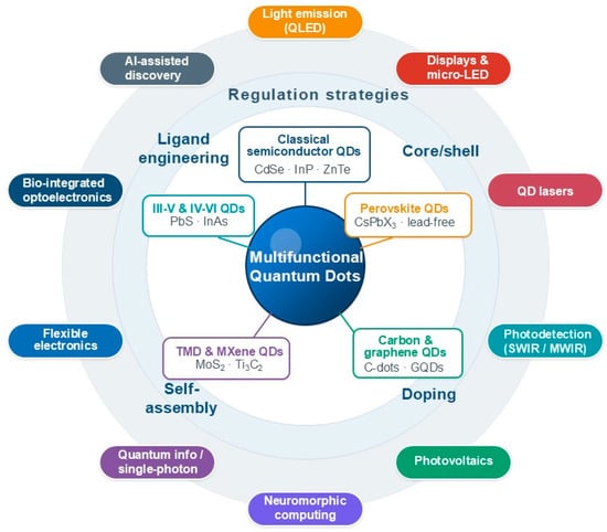
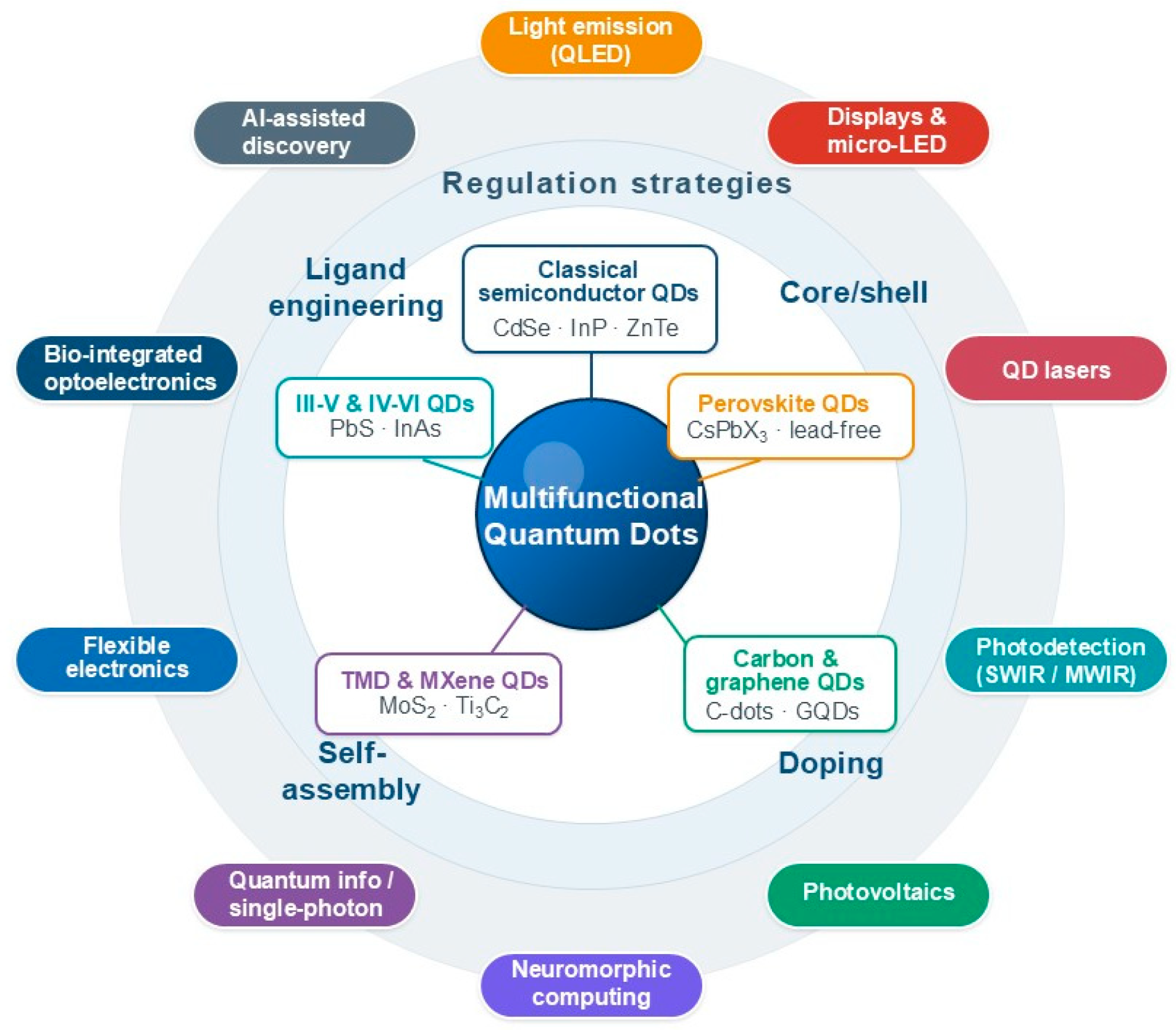
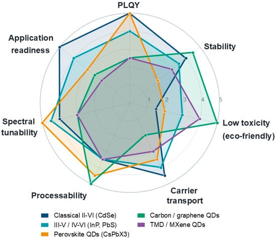
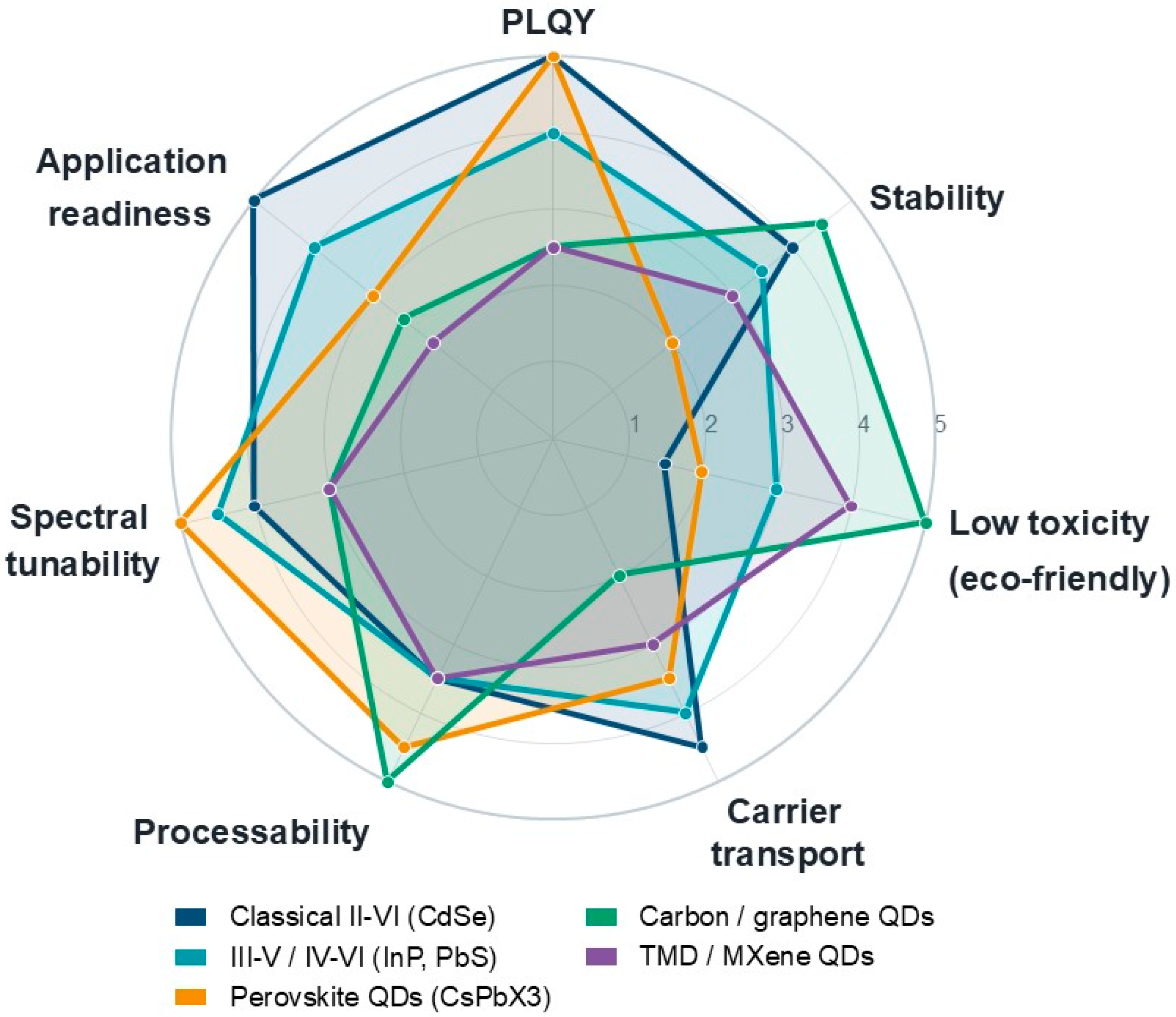
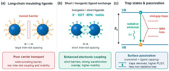
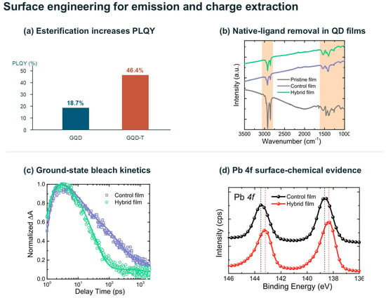
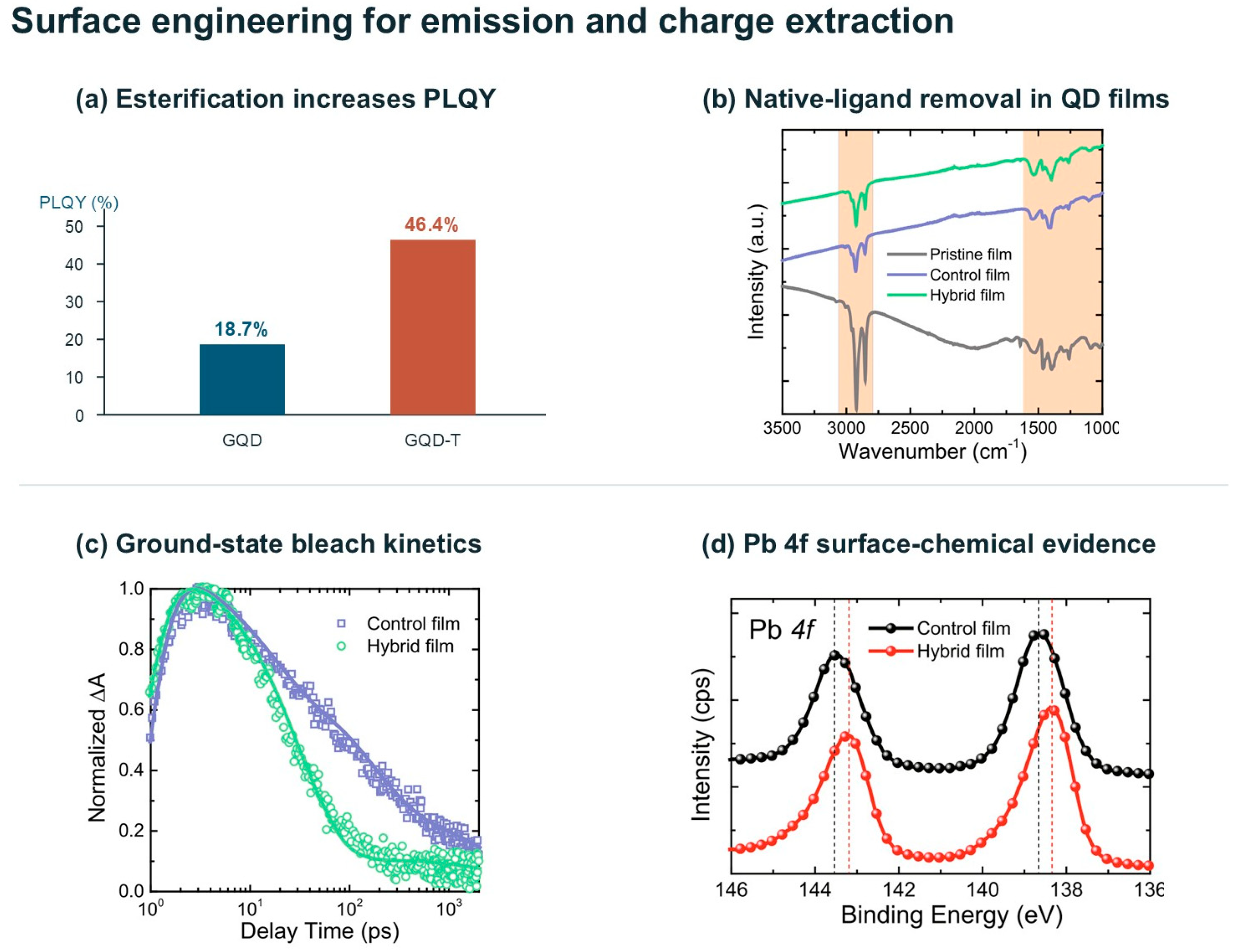
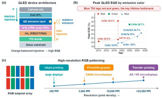
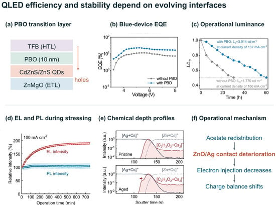
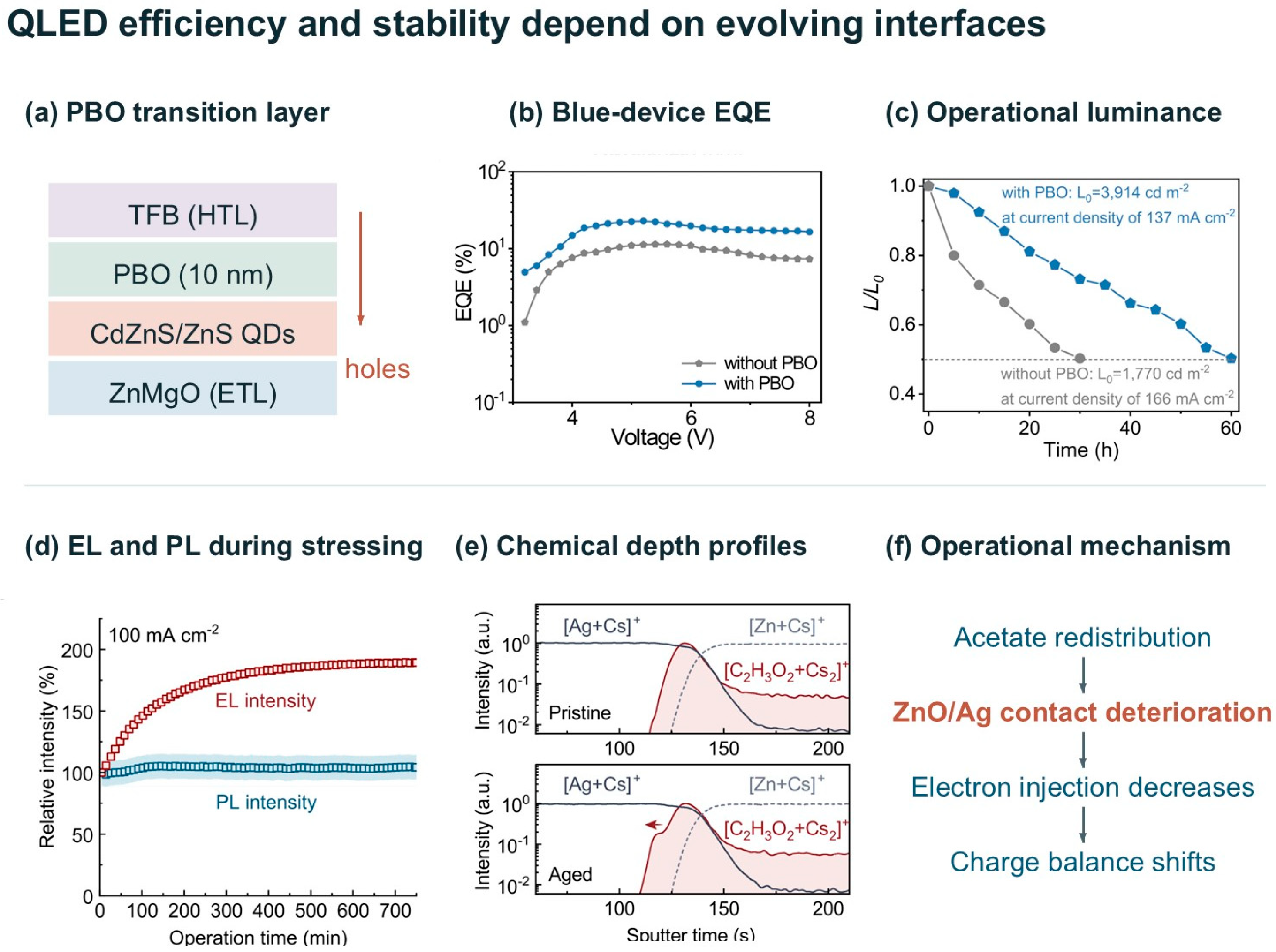
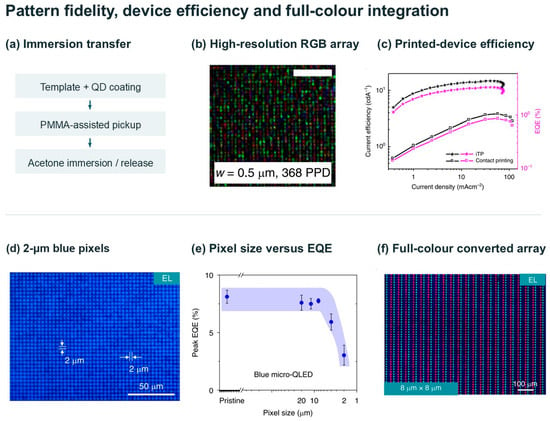
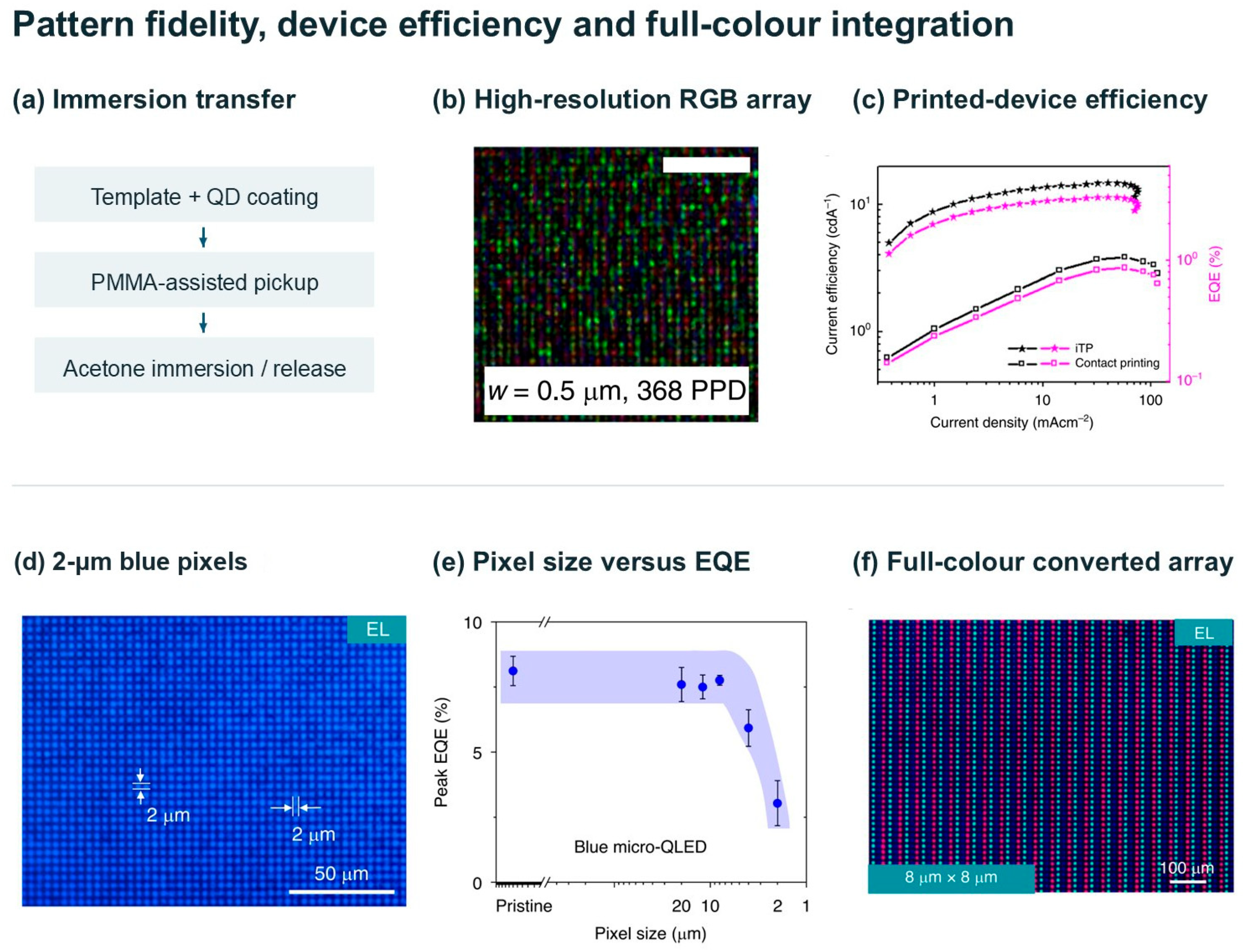
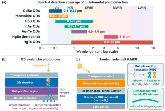
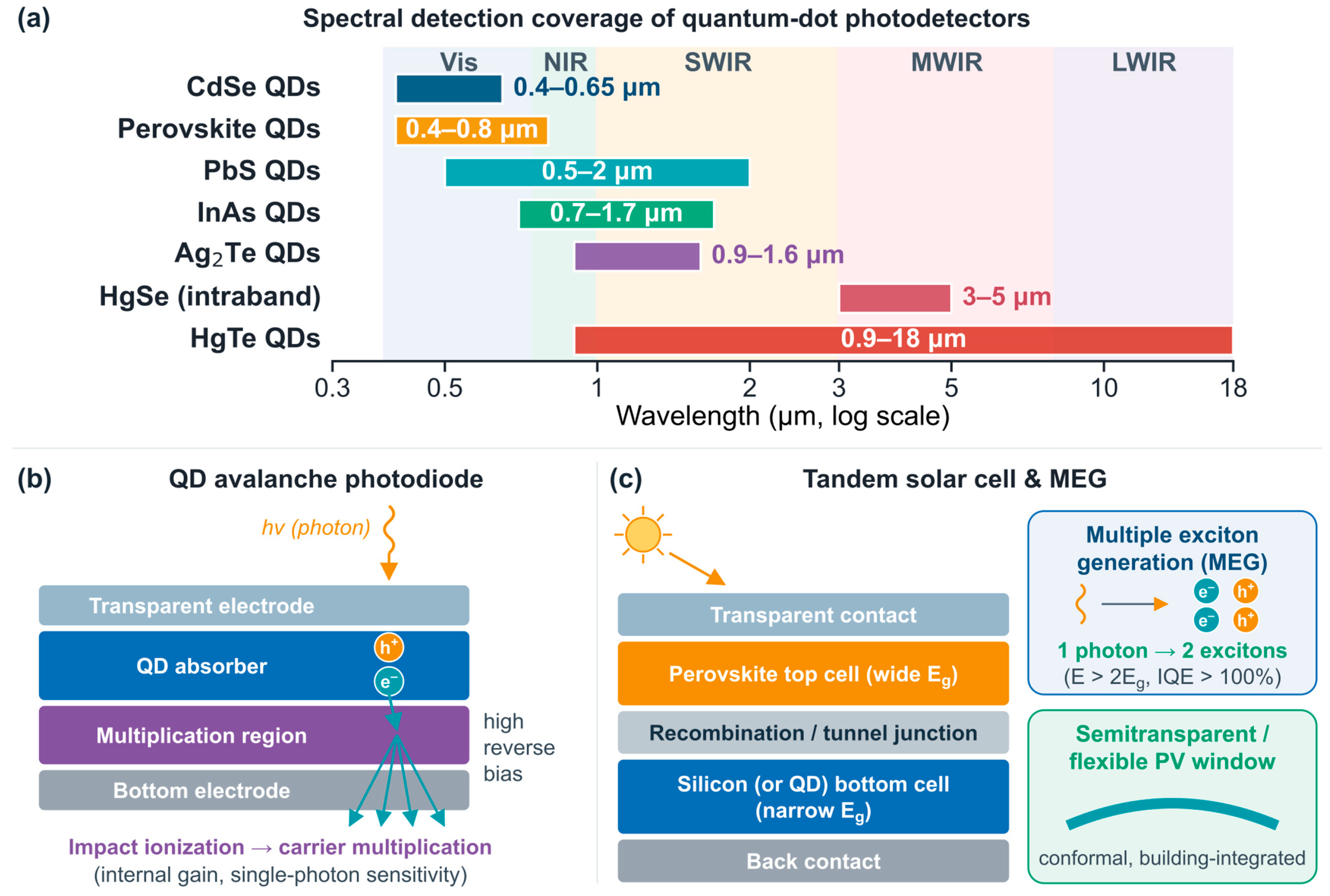
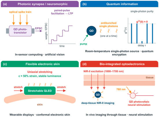
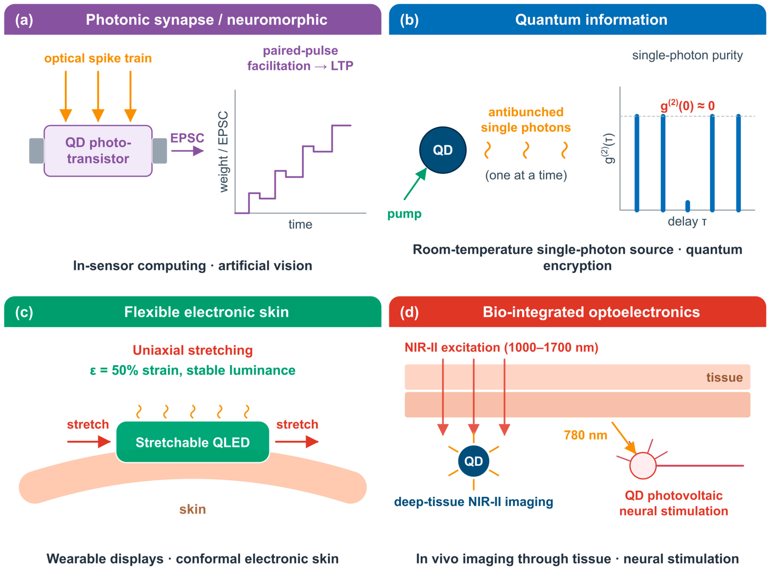
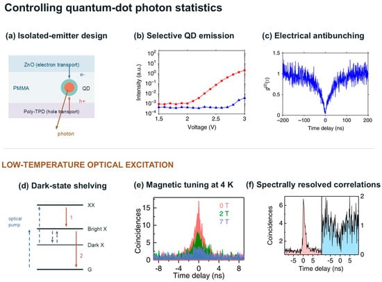
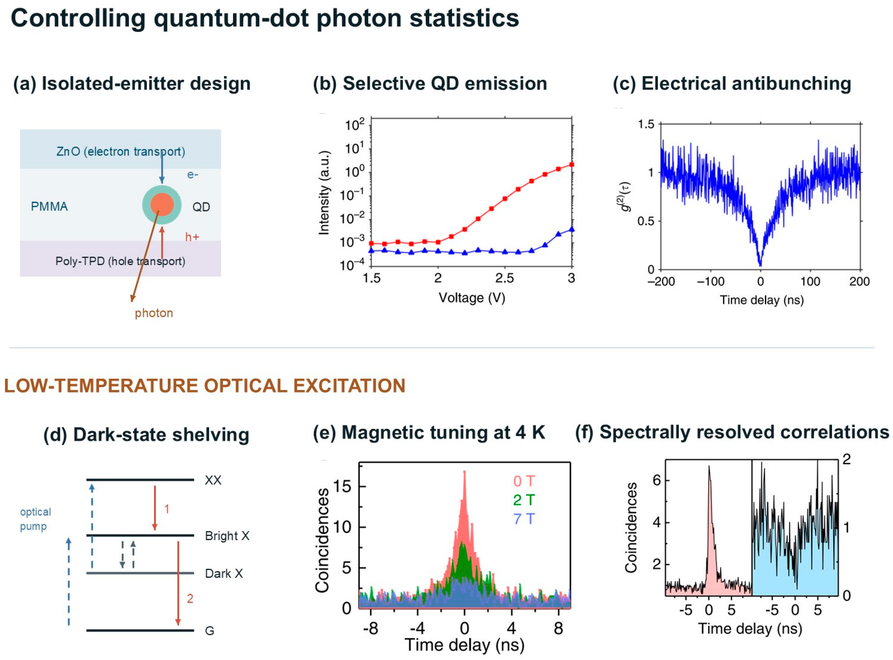
Disclaimer/Publisher’s Note: The statements, opinions and data contained in all publications are solely those of the individual author(s) and contributor(s) and not of MDPI and/or the editor(s). MDPI and/or the editor(s) disclaim responsibility for any injury to people or property resulting from any ideas, methods, instructions or products referred to in the content. |
© 2026 by the authors. Licensee MDPI, Basel, Switzerland. This article is an open access article distributed under the terms and conditions of the Creative Commons Attribution (CC BY) license.