


Abstract
This paper presents a novel extra-X second-generation current-controlled conveyor (EX-CCCII) with controllable current gain. Unlike the conventional EX-CCCII, the proposed EX-CCCII provides a controllable current gain between the - and -terminals. To demonstrate the advantages of the EX-CCCII with the controllable current gain, the proposed EX-CCCII is employed to realize a universal current-mode filter and a three-phase current-mode oscillator. The universal filter can realize five standard filtering responses (low-pass, high-pass, band-pass, band-stop, and all-pass) using the same topology. The current gains of these filters can be controlled through the current gain of the EX-CCCII, while the natural frequency of the universal filter can be electronically tuned via the intrinsic resistance at the x-terminal. When the proposed EX-CCCII is used to implement the three-phase oscillator, the condition of oscillation can be adjusted through the current gain of the EX-CCCII, whereas the oscillation frequency can be tuned using the parasitic resistance of the x-terminals. The proposed EX-CCCII and its applications were verified through SPICE simulations using the transistor model parameters NR100N (NPN) and PR100N (PNP) of the bipolar array ALA400-CBIC-R from AT&T to confirm the functionality and feasibility of the proposed topologies. Furthermore, experimental verification of the EX-CCCII and its integration into a three-phase oscillator further substantiates the proposed concept and demonstrates its practical viability.
1. Introduction
The second-generation current conveyor (CCII) is a flexible active building block that is particularly applicable for the implementation of circuits with both voltage- and current-mode [1,2]. Circuits based on the CCII have advantages over those based on the operational amplifier (op-amp). For example, they provide a wider signal bandwidth, higher slew rate, simpler structure, and lower power consumption [3,4]. A conventional CCII has three terminals, namely , , and , and the relation of these terminals can be given by and . The - and -terminals possess a high resistance (ideally infinite), and the -terminal possesses a low resistance (ideally zero). A conventional CCII has a single input and a single output terminal, which is a limitation for applications requiring the addition and subtraction of processed signals. These applications usually utilize many passive resistors, which are not well-suited for integrated circuits. To extend the capabilities of the CCII, the differential voltage current conveyor (DVCC) [5], the differential difference current conveyor (DDCC) [6], the fully differential second-generation current conveyor (FDCCII) [7], the dual-X second-generation current conveyor (DXCCII) [8], and the extra-X second-generation current conveyor (EX-CCII) [9] have been introduced. DVCC, DDCC, and FDCCII-based circuits easily allow the addition and subtraction of voltage signals, which is advantageous for feedback connections. The FDCCII and DXCCII can provide differential input and differential output current signals between the - and -terminals, while the EX-CCII can provide several independent current signals between the - and -terminals. The EX-CCII is a flexible active device that can offer several independent current signals between the - and -terminals in a single circuit. In the literature, the EX-CCII is featured in various applications, such as in first-order all-pass filters [10,11,12], precision rectifiers [13,14,15], analog multipliers [16], controller circuits [17], square/triangular wave generators [18], fractional-order circuits [19,20], and universal filters [21]. However, the parasitic resistance at the x-terminal of the EX-CCII is typically not utilized as a tuning parameter in practical applications. Consequently, external passive resistors are usually required, making electronic tuning difficult to achieve.
The parasitic resistance at the -terminals of the EX-CCII can be advantageously used as a tuning parameter to reduce the number of external passive resistors and enable the electronic tuning capability for applications. The extra-X current-controlled current conveyor (EX-CCCII) was introduced in [22]. In the EX-CCCII, the number of parasitic resistances at the -terminals is equal to the number of -terminals. This EX-CCCII has been implemented in many current-mode analog signal processing circuits, examples including instrumentation amplifiers [23,24], precision rectifiers [25], immittance simulators [26], first-order all-pass filters [27], universal filters [28,29,30,31,32,33,34], oscillators [35,36,37], and fractional-order circuits [19]. A single EX-CCCII can provide several pairs of - and -terminals, where the parasitic resistances at the -terminals are identical in the ideal case. However, the current gain between the - and -terminals is still equal to one, i.e., .
Therefore, in this paper, an EX-CCCII with controlled current gain is proposed to enhance the capability of the EX-CCCII. Unlike the conventional EX-CCCII, the proposed device provides a current gain between the - and z-terminals. Furthermore, this current gain can be electronically controlled while preserving the key features of the original EX-CCCII, namely multiple - and -terminals and the parasitic resistance at the -terminal. To the best of our knowledge, this concept has not yet been applied to the EX-CCCII, which constitutes the main contribution of this work. In order to highlight the improvements of the newly proposed EX-CCCII, it was used to realize a universal current-mode filter and a three-phase oscillator. For the universal current-mode filter, the current gain of the EX-CCCII can be used to electronically control the current gain of the filter transfer functions, and the bias current of the EX-CCCII can be used to electronically control the natural frequency of the universal filter. For the quadrature oscillator, the oscillation condition can be controlled by the current gain of the EX-CCCII, and the oscillation frequency can be controlled electronically by the bias current of the EX-CCCII. The proposed current-gain controlled EX-CCCII, and its application to a universal filter and a quadrature oscillator were simulated and designed using SPICE and model process parameters of the NR100N (NPN) and PR100N (PNP) bipolar array transistors ALA400-CBIC-R from AT&T to confirm the functionality and feasibility of the new circuits.
2. Proposed Circuit
2.1. EX-CCCII with Controlled Current Gain
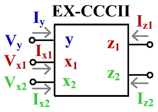
Figure 1 shows the electrical symbol of the conventional EX-CCCI [22]. Its port characteristics can be expressed by
It should be noted that the device provides two independent relationships between the - and -terminals, i.e., and , with two parasitic resistances and appearing at the - and -terminals, respectively. In general, multiple relationships between the - and -terminals can be realized, i.e., , …, , where denotes the number of terminal pairs [19].
Figure 1.
Electrical symbol of conventional EX-CCCII.
A conventional CCII/CCCII that offers current gain between the - and -terminals has been introduced [38,39,40,41,42]. The circuits in [38,39] are realized using active devices, whereas the circuit in [40] is implemented using bipolar technology, and the circuits in [41,42] are implemented using CMOS technology. However, conventional CCII/CCCII with controlled current gain in [38,39,40,41,42] provide only a single current gain between the x- and z-terminals per CCII/CCCII. In this work, the concept of a CCII/CCCII with controllable current gain is adopted to modify the conventional EX-CCCII [22], enabling multiple controllable current gains between the x- and z-terminals. Consequently, the proposed EX-CCCII can provide multiple current gains between the x- and z-terminals. The concept used to obtain current gain in [40] is adopted in this work.
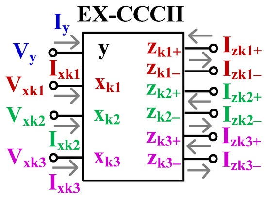
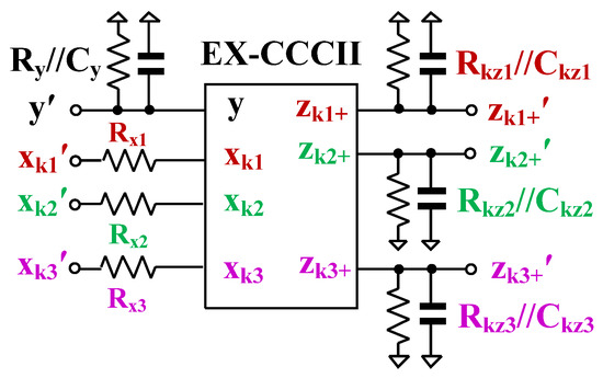
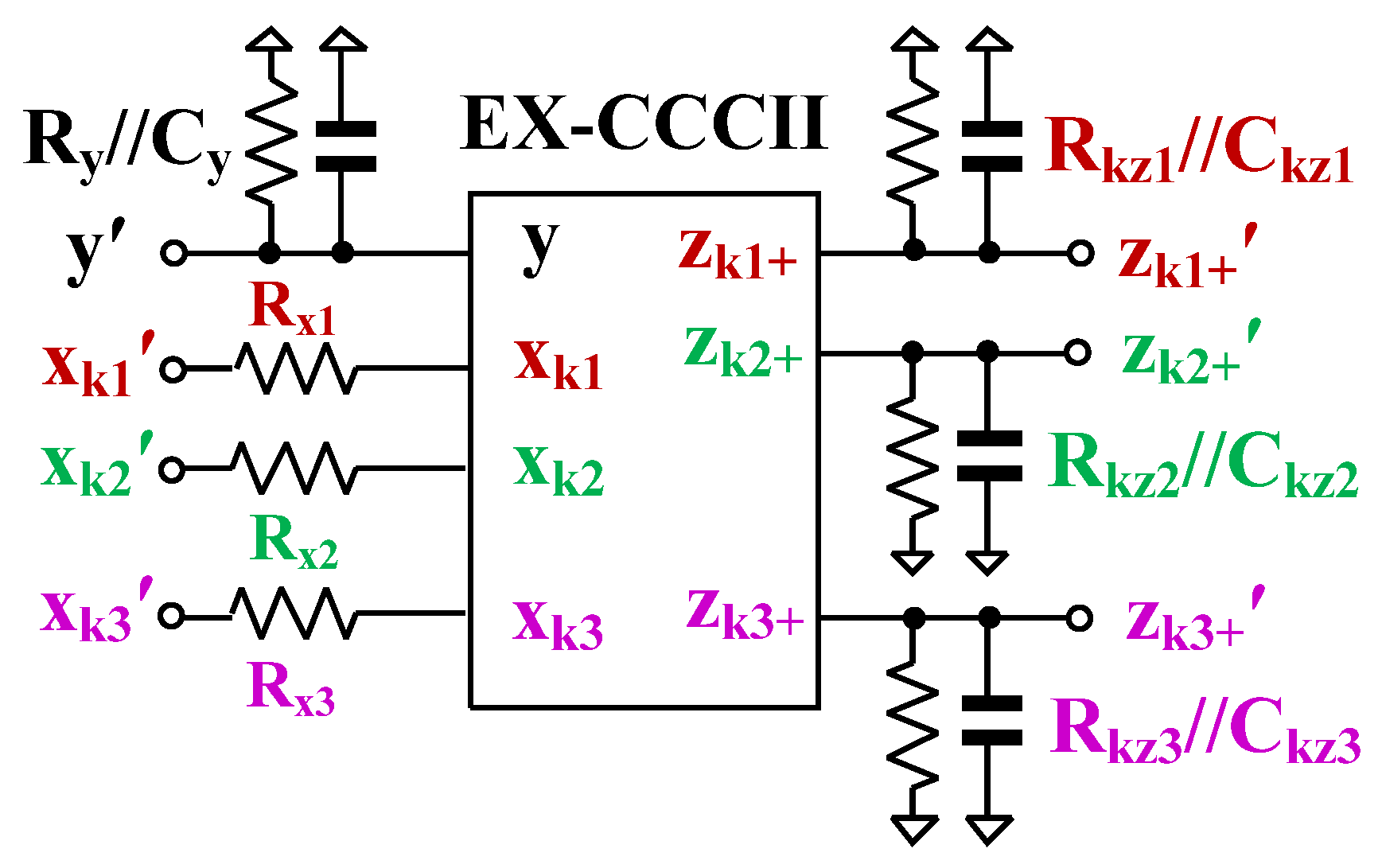
Figure 2 shows the electrical symbol of the proposed EX-CCCII with controllable current gain. Its characteristics are similar to those of the conventional EX-CCCII [22], except that it enables a controllable current gain between the - and -terminals. The proposed EX-CCCII establishes three independent relationships between the - and -terminals, and provides three current gains . The parasitic resistances appear at the -terminals, where . It should be noted that the three current gains can be independently controlled. In addition, the device provides both positive- and negative-type output currents at the -terminal, denoted as and , respectively.
Figure 2.
Electrical symbol of the proposed EX-CCCII.
The port characteristics of the device in Figure 2 can be expressed as follows:
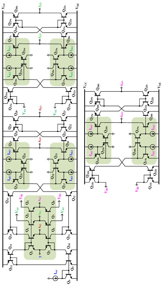
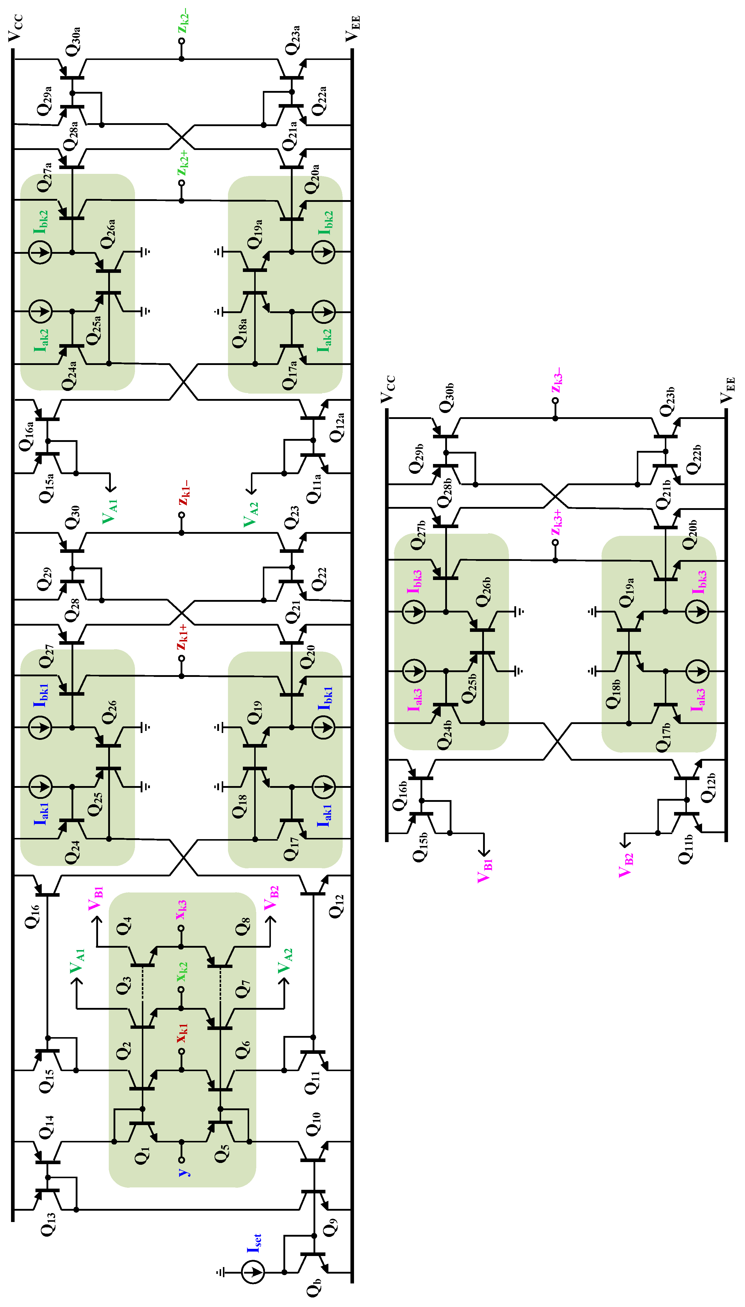
Figure 3 shows a possible implementation of the EX-CCCII with a controlled current gain that corresponds to Figure 2. Transistors Q1 to Q8 create a translinear loop, and transistors Qb, Q9, Q10, Q13, Q14, and work as current sources to properly bias this translinear loop.
Figure 3.
BJT implementation of the EX-CCCII with controlled current gain.
Assuming that transistors Q1–Q8 are identical, and that transistors Qb, Q9, Q10, Q13, and Q14 are well matched, with their collectors connected to load transistors, the following relationships can be obtained: , , and . Accordingly, the parasitic resistances , , and can be expressed as given in [43].
where is the bias current of the EX-CCCII and is the thermal voltage (≈26 mV).
The current amplifier between the - and -terminals is realized by current mirrors Q11–Q12, Q15–Q16, Q17–Q20, and Q24–Q27, where Q17–Q20 and Q24–Q27 form current mirrors that provide current gain [4]. Assuming all transistors are well matched, the current gain between the - and -terminals is given in [40].
It should be noted that the current gain can be electronically controlled via the ratio .
Note that the -terminal provides a positive current gain, whereas the -terminal provides a negative current gain. The negative output is realized using cross-coupled (inverting) current mirrors Q21–Q23 and Q28–Q30. It should also be noted that multiple - and -terminals can be obtained by employing current mirrors implemented with complementary NPN and PNP transistors. Accordingly, the current relationship between the - and -terminals can be expressed as .
The current gains between the - and -terminals and the - and -terminals are realized using current mirrors similar to those used for . The second current gain stage, between the - and -terminals, is implemented using current mirrors Q11a–Q12a, Q15a–Q16a, Q17a–Q20a, and Q24a–Q27a. Similarly, the third current gain stage, between the - and -terminals, is realized using current mirrors Q11b–Q12b, Q15b–Q16b, Q17b–Q20b, and Q24b–Q27b. Transistor groups Q17a–Q20a, Q24a–Q27a, and Q17b–Q20b, Q24b–Q27b form current mirrors with a current gain of four. Assuming that these transistors are identical, the current gain between the - and -terminals and - and -terminals can be given, respectively, by [40]
The cross-coupled current mirrors (Q21a–Q23a, Q28a–Q30a and Q21b–Q23b, Q28b–Q30b) provide negative current gains at the and -terminals. As discussed previously for obtaining multiple -terminals, multiple - and -terminals can be realized using current mirrors implemented with complementary NPN and PNP transistors. Therefore, it can be concluded that the circuit in Figure 3 provides multiple current gains, , , and , which can be independently controlled. By employing the concept of multiple terminals reported in [19], the proposed circuit can be extended to realize the -th - and -terminals with a corresponding current gain for the intended applications.
2.2. EX-CCCII with Its Parasitic Components
Taking into account non-idealities, the considered EX-CCCII can be described by the following equation:
where is the voltage transfer gain from the - to -terminals, is the current transfer gain from the to -terminals, and = 1, 2, 3. Ideally, and are equal to 1; however, in practice, these parameters suffer from tracking errors that can be expressed by , , where represents the voltage tracking error and represents the current tracking error.
Figure 4 shows the EX-CCCII, including its parasitic components at high frequencies. Here, and denote the parasitic capacitance and resistance at the -terminal, respectively, while and represent the parasitic capacitance and resistance at the -terminal, respectively .
Figure 4.
EX-CCCII with its parasitic components.
2.3. Applications of the EX-CCCII
2.3.1. Current-Mode Universal Filter
Universal filters using CCII/CCCII with a controlled current gain have been introduced in [42,44]. The current gain of the CCII can be used to control the magnitude of the transfer functions [42] and the quality factor [44] of the filters. The filters in [42] employ three CCIIs while those in [44] employ two CCCIIs.
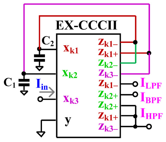
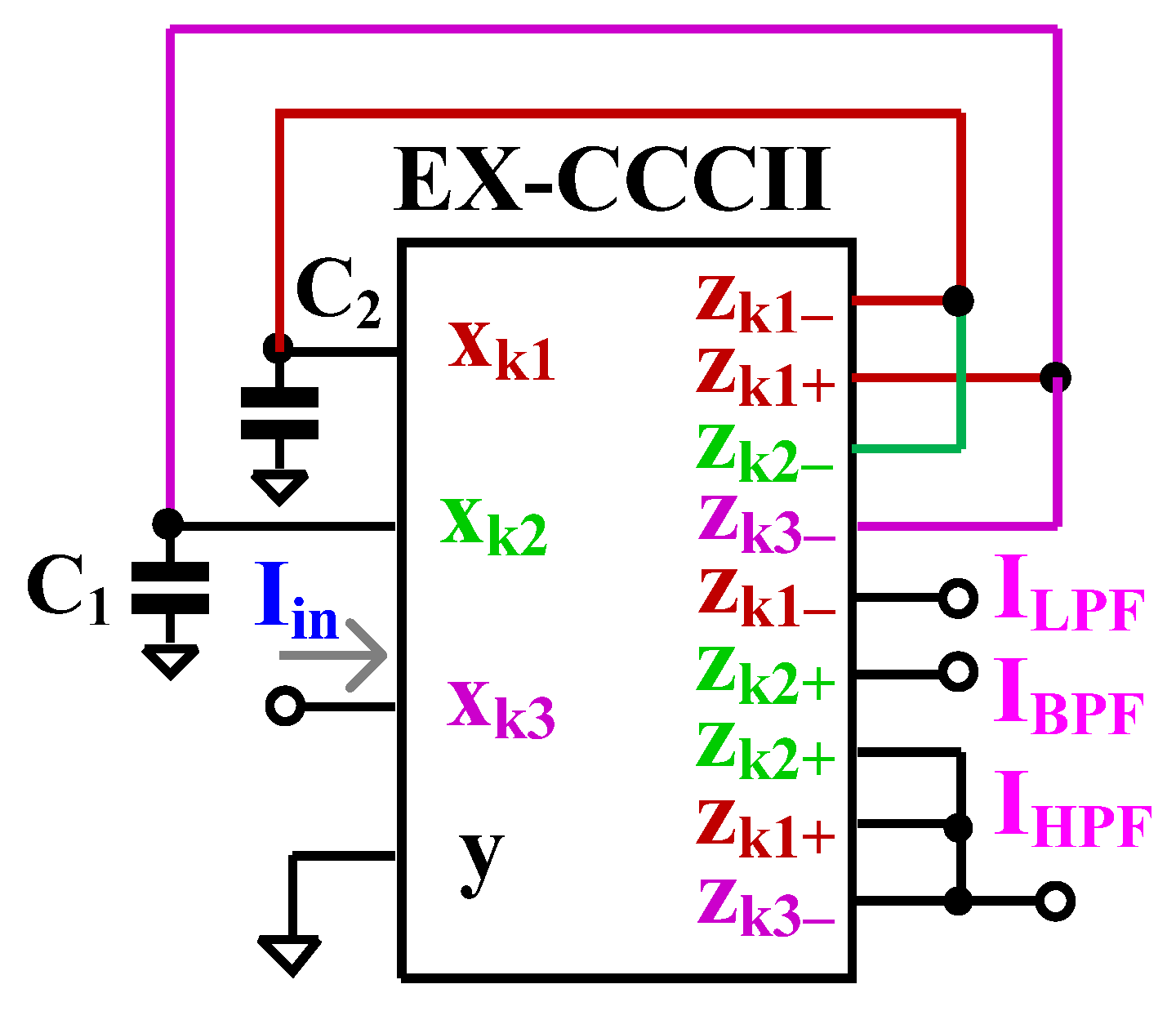
Since the proposed EX-CCCII with the controllable current gain in Figure 3 exhibits three parasitic resistances, , , and , as well as three independent current gains, , , and , it is well suited for the implementation of a current-mode universal filter. Figure 5 shows the proposed current-mode universal filter using an EX-CCCII with a controlled current gain as the active building block. It uses only a single EX-CCCII and two grounded capacitors. The circuit is based on two-integrator loops: and , which works as a lossless integrator, and and , which works as a lossy integrator. The resistance is not utilized. The circuit offers low-input impedance and high-output impedance, which is required by current-mode circuits. It can realize a low-pass filter (LPF), band-pass filter (BPF), high-pass filter (HPF), band-stop filter (BSF), and all-pass filter (APF) in the same topology through the proper selection of the output terminals. The current gain of the EX-CCCII can be used to adjust the magnitude of the transfer functions of the filters.
Figure 5.
The proposed current-mode universal filter.
By setting and applying (1) along with nodal analysis, the output of the current-mode universal filter in Figure 5 can be expressed as follows:
The BSF can be obtained by as:
The APF can be obtained by as:
The natural frequency ( and the quality factor ( can be, respectively, given as:
The current gain of the transfer functions (H(s)) can be expressed as:
It is evident from (13) and (14) that can be electronically controlled by and (with ) via the bias current . The quality factor is determined by the ratio , while the current gain of the transfer functions can be electronically controlled by .
Using non-idealities of EX-CCCII in (7) and EX-CCCII with its parasitic components in Figure 4, the denominator of filtering functions can be expressed as:
where denotes the current transfer gain from the -terminal to the -terminal, and denotes the current transfer gain from the -terminal to the -terminal, for . The parasitic capacitances at the and terminals affect the capacitance , resulting in . Similarly, the parasitic capacitances at the and terminals affect the capacitance , yielding .
The non-ideal natural frequency () and quality factor () of the filter can be, respectively, expressed as:
The non-ideal current gains of all transfer functions are give as:
The effects of parasitic capacitances can be mitigated by choosing and .
The active and passive sensitivities of the filter, with respect to the parameters of the natural frequency and quality factor, are expressed in Table 1 and Table 2.
Table 1.
Active and passive sensitivities of .
Table 2.
Active and passive sensitivities of .
2.3.2. Current-Mode Three-Phase Oscillator
The multiphase sinusoidal oscillators (MSO) can be realized using variant sub-circuits, such as a first-order APF [45], first-order LPF [46], or first-order HPF [47]. The MSO-based CCCII, with the controlled current gain, has been introduced in [48]. The system is based on a first-order LPF with the current gain of the CCCII being used to control the condition of oscillation. To realize a three-phase oscillator, the system employs three CCCIIs and three grounded capacitors. Since the proposed EX-CCCII, with a controlled current gain, possesses parasitic resistances, , , and , as well as three current gains, , , and , it can be used to realize a current-mode three-phase oscillator.
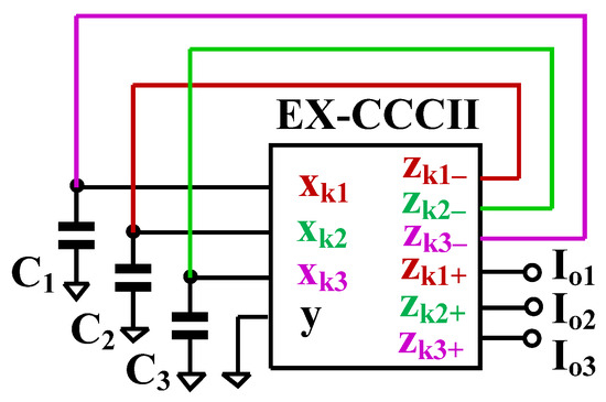
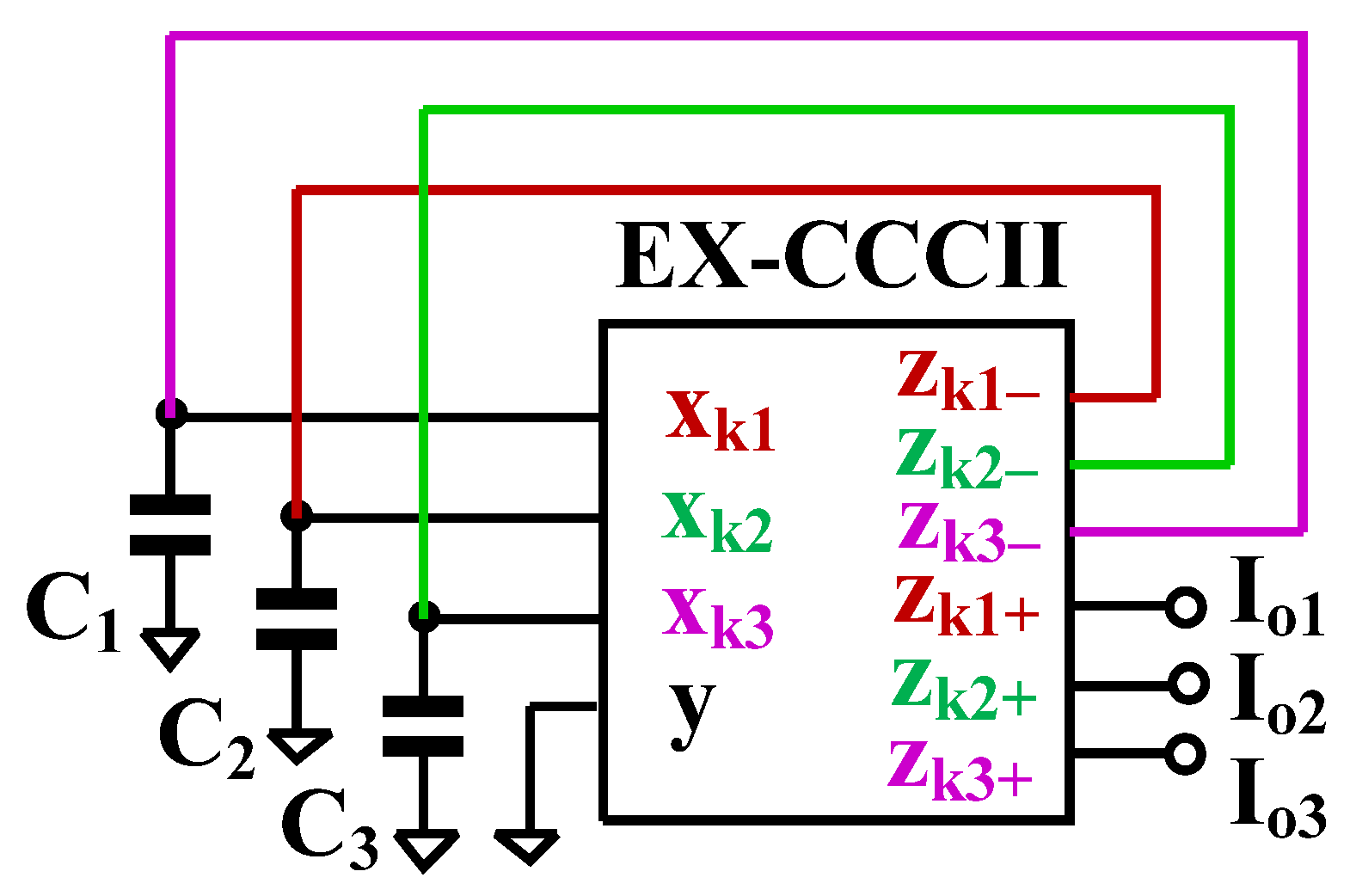
Figure 6 shows the proposed current-mode three-phase oscillator realized using three first-order LPFs. The system uses an EX-CCCII with a controlled current gain that has three associations between the - and -terminals (). Thus, the EX-CCCII has three independent current gains, , , and , and three parasitic resistances, , , and .
Figure 6.
Proposed current-mode three-phase oscillator.
Letting , , and , the loop-gain of the system in Figure 6 can be expressed as:
Assuming unity loop gain, we obtain the following condition:
Or:
Letting the current gain be:
The system can generate a frequency of:
Thus, the condition of oscillation can be given by , and the frequency of oscillation can be controlled by . Both parameters can be electronically controlled, which can easily compensate for the effects of tracking errors of the EX-CCCII, temperature variation, and process variations. The circuit can generate three output waveforms with equal amplitude, out of phase with each other by 120 degrees at the oscillating frequency.
By taking into account the non-ideal and parasitic parameters of the EX-CCCII with controlled current gain, the three-phase oscillator can be re-evaluated. Assuming that , where represents the current transfer gain from the -terminal to the -terminal , the non-ideal loop gain of the oscillator shown in Figure 6 becomes:
Or:
Here, , where denotes the parasitic capacitance at the -terminal .
It follows from (26) that the current gain errors affect the condition of oscillation of the oscillator system. However, by employing the EX-CCCII with a controlled current gain, this issue can be mitigated through the appropriate adjustment of the current gain. The parasitic capacitances , , and affect the oscillation frequency. To reduce their impact, the conditions , , and should be satisfied.
3. Results
3.1. Simulation Results
The proposed EX-CCCII with controlled current gain and its applications to a current-mode universal filter and current-mode sinusoidal oscillator were simulated and designed by SPICE and the transistor model parameters of AT&T’s ALA400 CBIC-R [49]. The supply voltage was ±1.2 V.
The performance of the EX-CCCII was investigated. The setting current was set to 25 μA, the biasing current was set to 20 μA, and the biasing current was used to vary the current gain of the EX-CCCII (). The performances of the -, -, -terminals of EX-CCCII are evaluated.
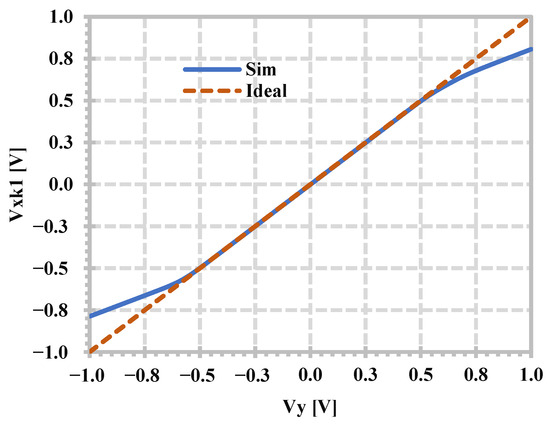
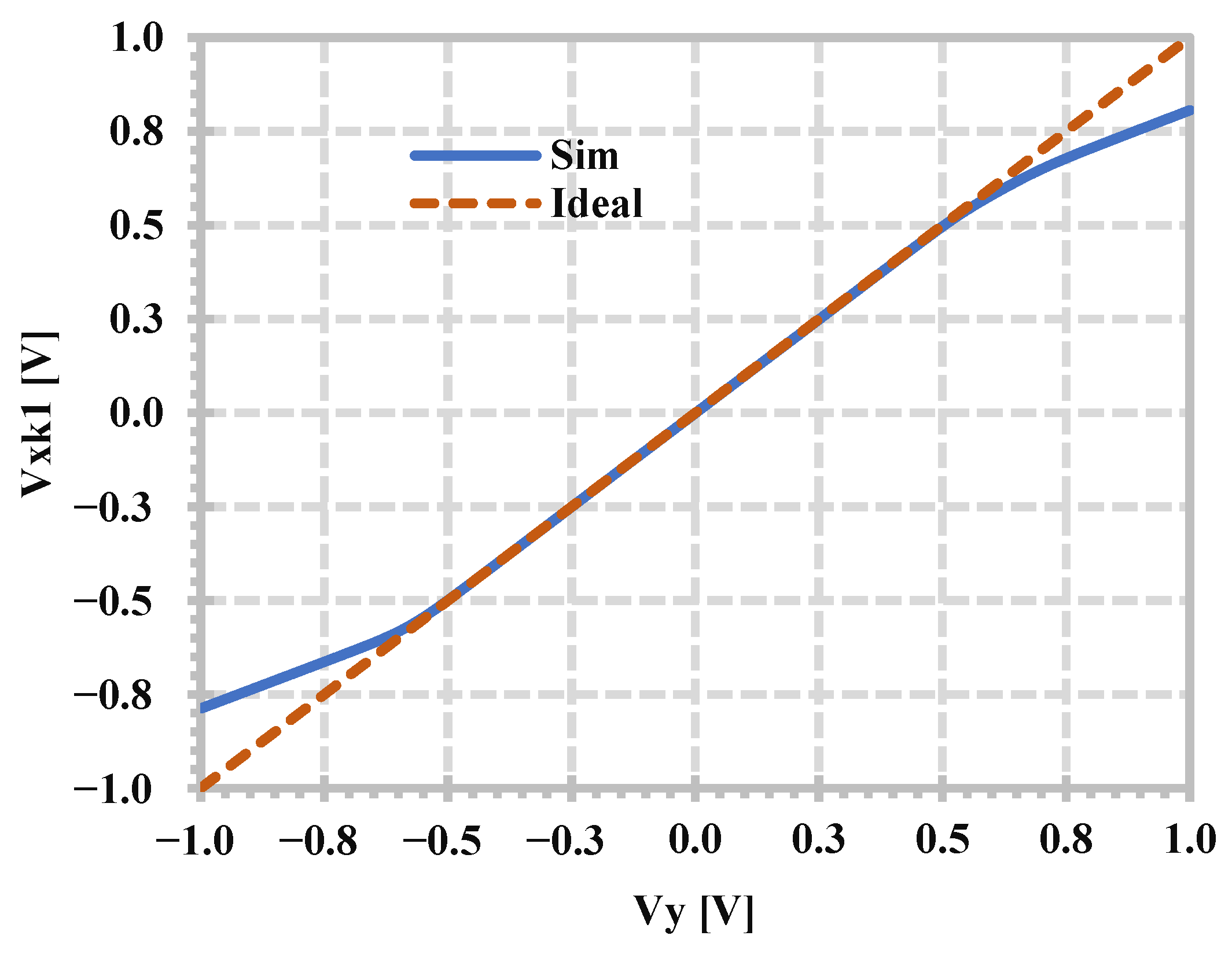
Figure 7 shows the – characteristic of the proposed EX-CCCII compared to the ideal characteristic. The linear operating range of is approximately ±0.5 V. When , an offset voltage of −35 µV is observed. For , in the range of −0.5 V to 0.5 V, the voltage error is less than 4.38 mV.
Figure 7.
DC transfer characteristics versus showing the ideal and simulated input voltage range.
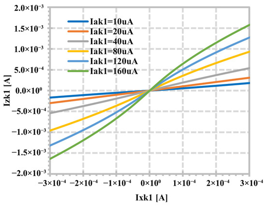
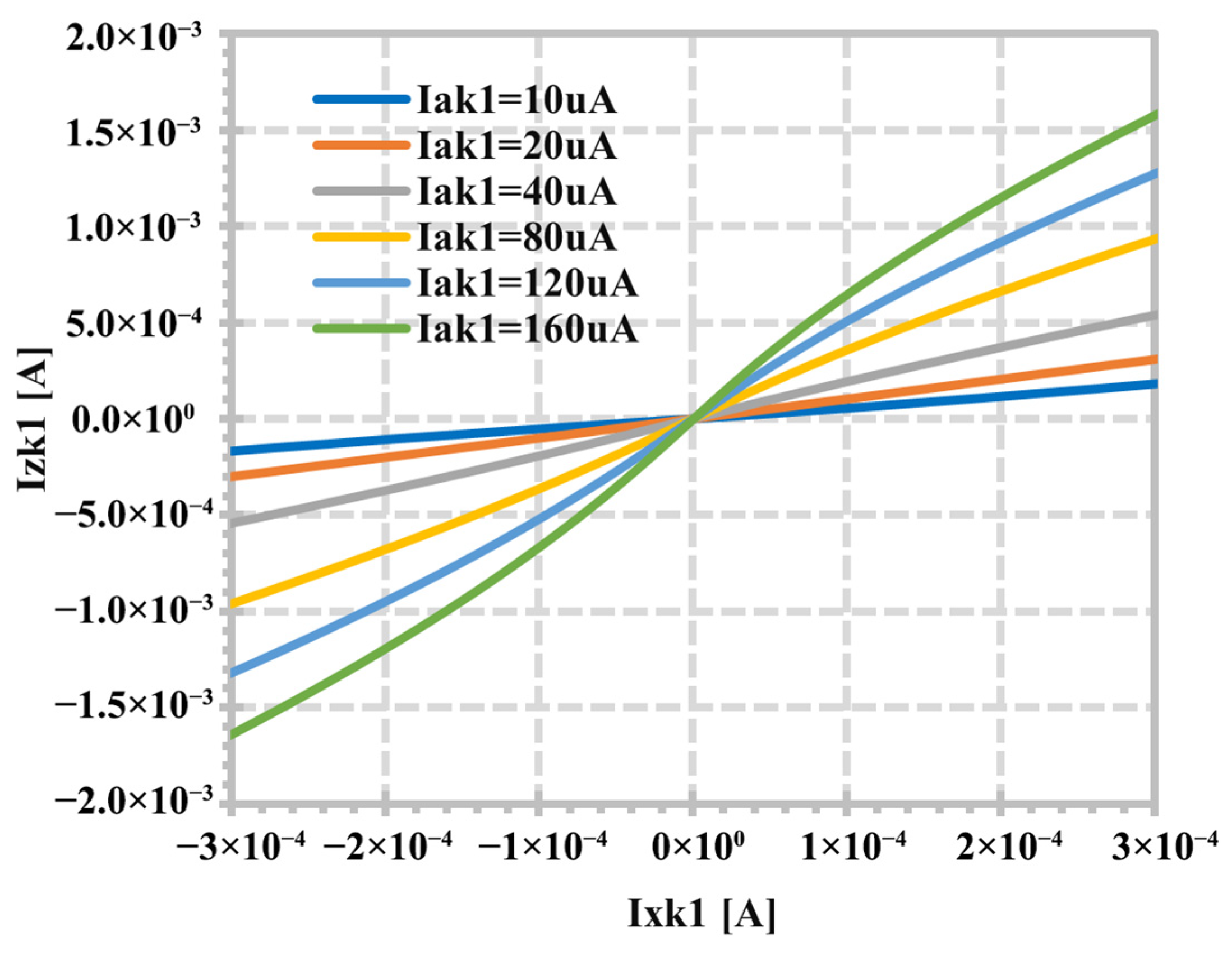
Figure 8 shows the – characteristic of the proposed EX-CCCII for biasing currents set to 10, 20, 40, 80, 120, and 160 µA. At a unity current gain ( µA), the current gain error is 0.57%. When the current gain is increased to 8 ( µA and µA), the error rises to 11.34%.
Figure 8.
DC transfer characteristics versus with different gain .
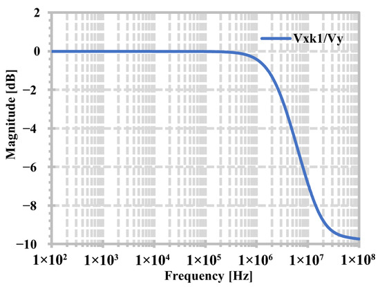
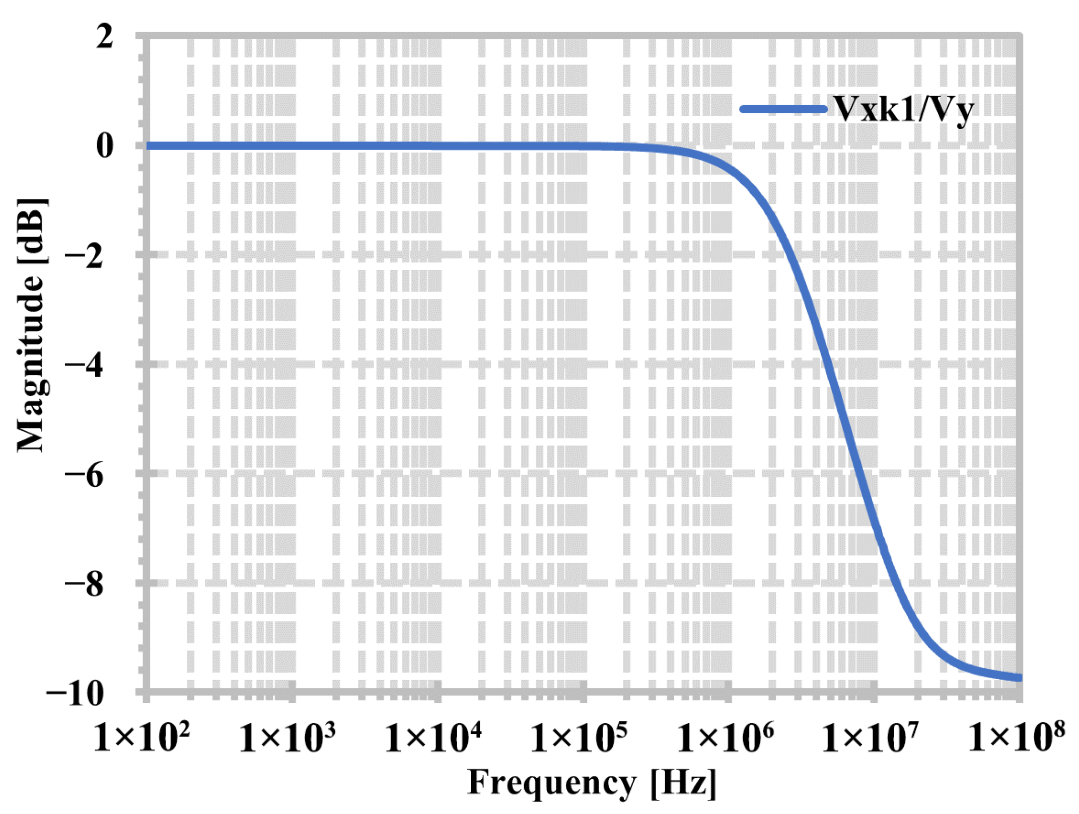
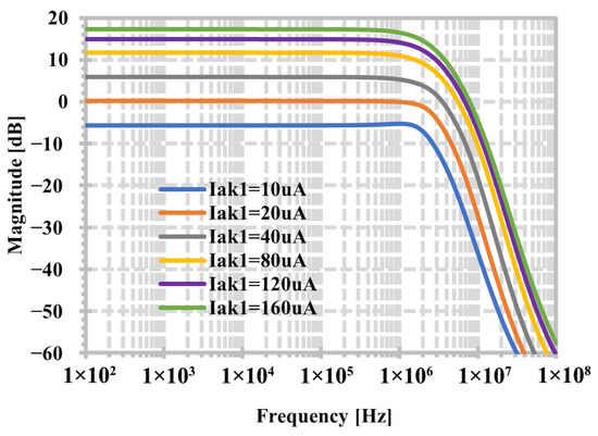
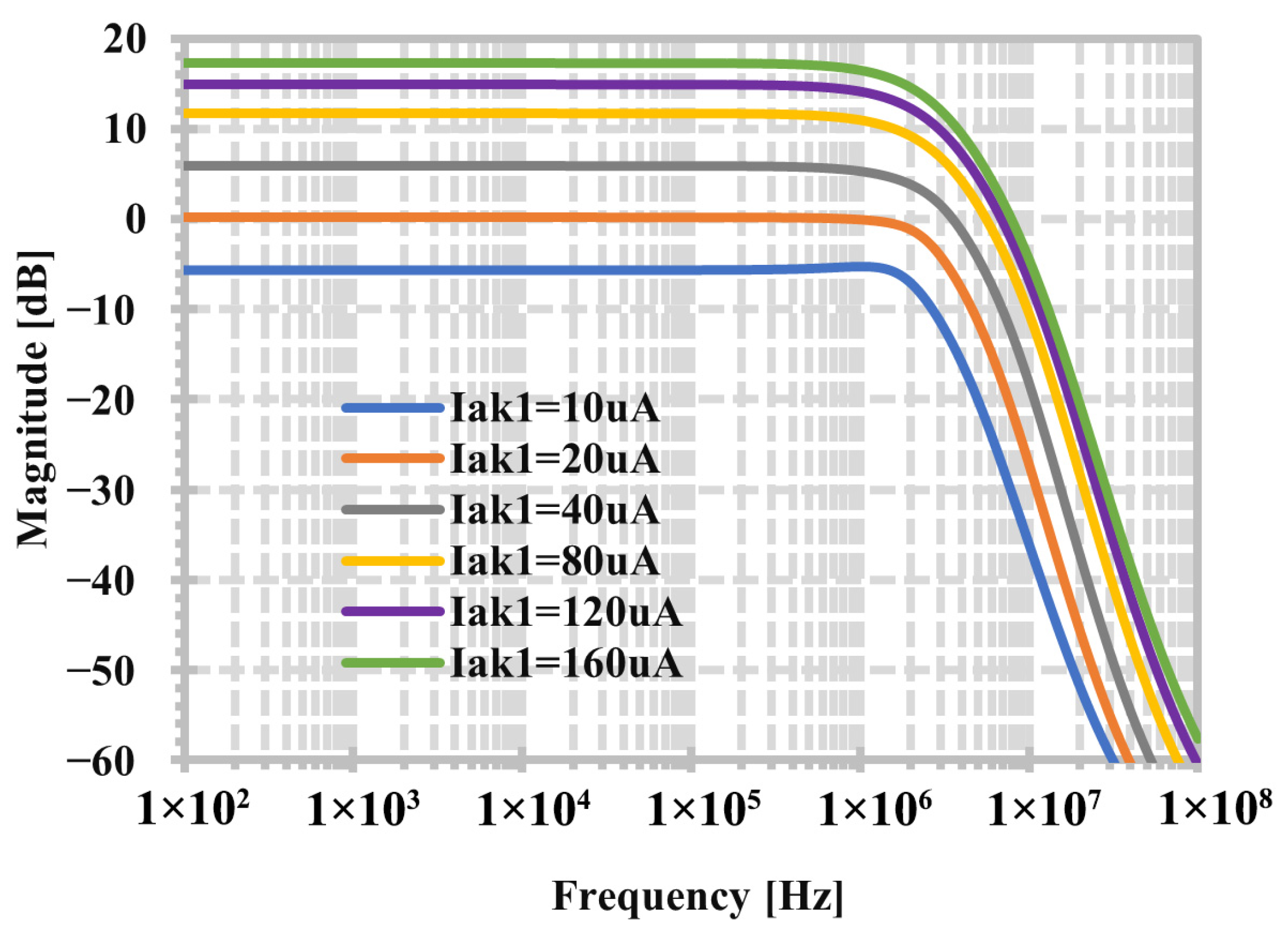
Figure 9 shows the simulated magnitude characteristic of the voltage gain of the EX-CCCII. The cut-off frequency of the voltage gain was 3.6 MHz. Figure 10 shows the simulated magnitude characteristic of the current gain with a varying EX-CCCII gain, accomplished by setting = [10, 20, 40, 80, 120, 160] μA. The cut-off frequency of the current gain was 2.66 MHz. In practical implementations, when the biasing current is increased to achieve a higher current gain, a discrepancy between the simulated and expected values may arise due to the non-ideal characteristics of BJTs, including finite a current gain (), early voltage, and base current mismatch in the current mirrors. These effects introduce errors in the realized current gain parameters.
Figure 9.
Magnitude characteristic of the voltage gain .
Figure 10.
Magnitude characteristic of the current gain with different .
However, thanks to the wide electronic tuning capability of the proposed circuit, the desired current gain can be effectively compensated by appropriately adjusting the biasing current . Therefore, despite the presence of non-idealities, the circuit can still achieve the required current gain with acceptable accuracy in practical applications.
At a nominal bias current of , the total power dissipation of the proposed EX-CCCII with controlled current gain was 2.34 mW.
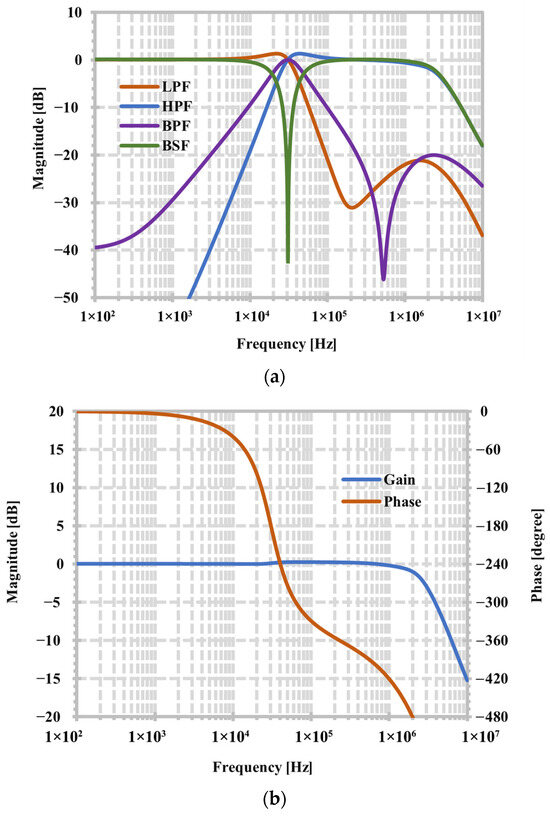
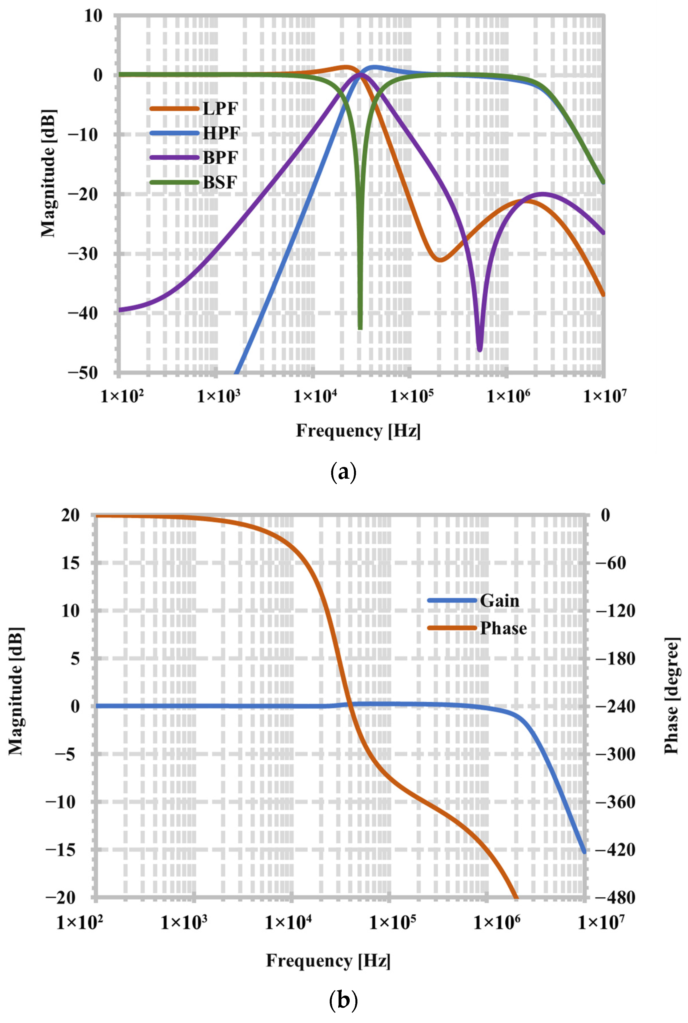
The proposed current-mode universal filter in Figure 5 was simulated. The capacitance value of and were 9 nF. Figure 11 shows the simulated magnitude frequency responses of the LPF, BPF, HPF, BSF, and APF when the setting current 25 μA and the biasing currents 20 μA. The simulated natural frequency was 30.9 kHz, whereas the theoretical value was 34 kHz. This deviation is mainly attributed to the non-ideal current transfer gains of the EX-CCCII with the controlled current gain, as described by (17). The circuit consumed 1.5 mW of power.
Figure 11.
Gain and phase frequency responses of the current-mode filter: (a) LPF, HPF, BPF, BSF, and (b) APF.
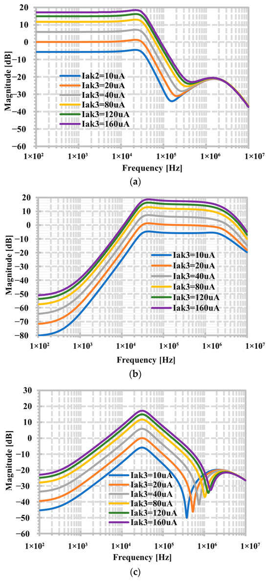
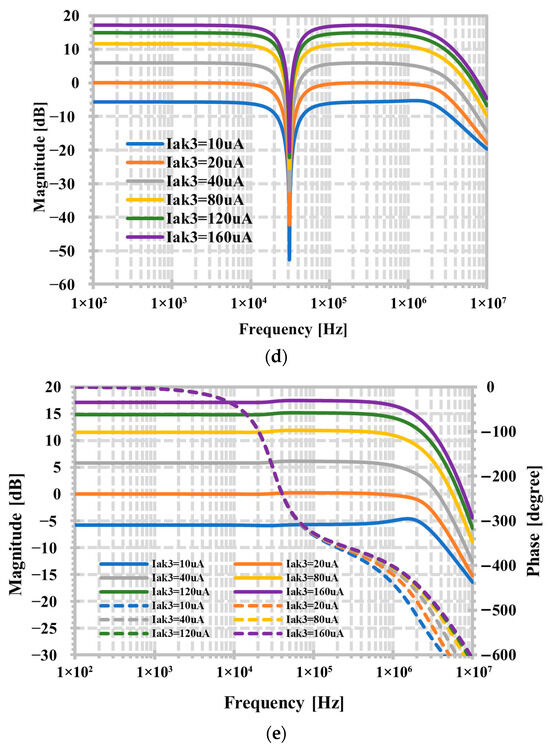
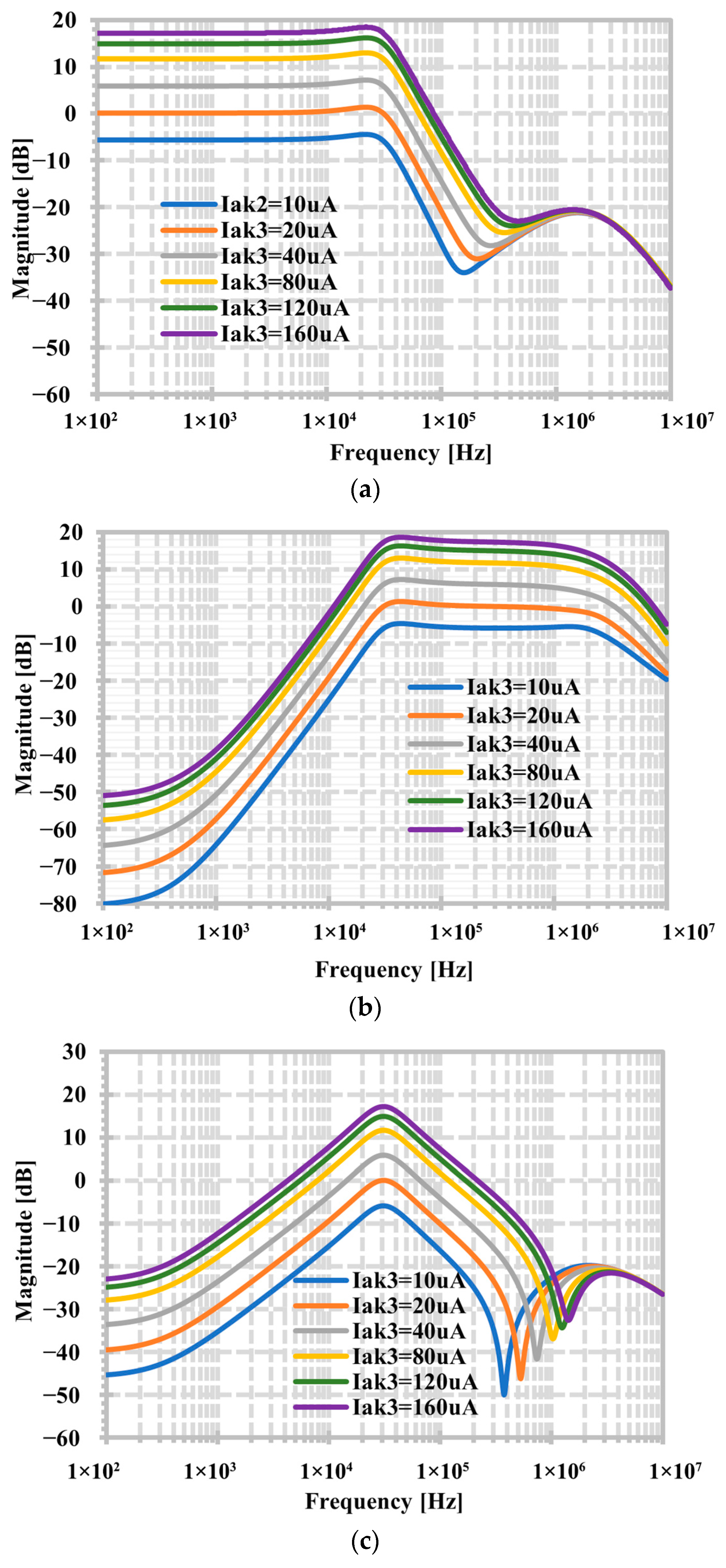
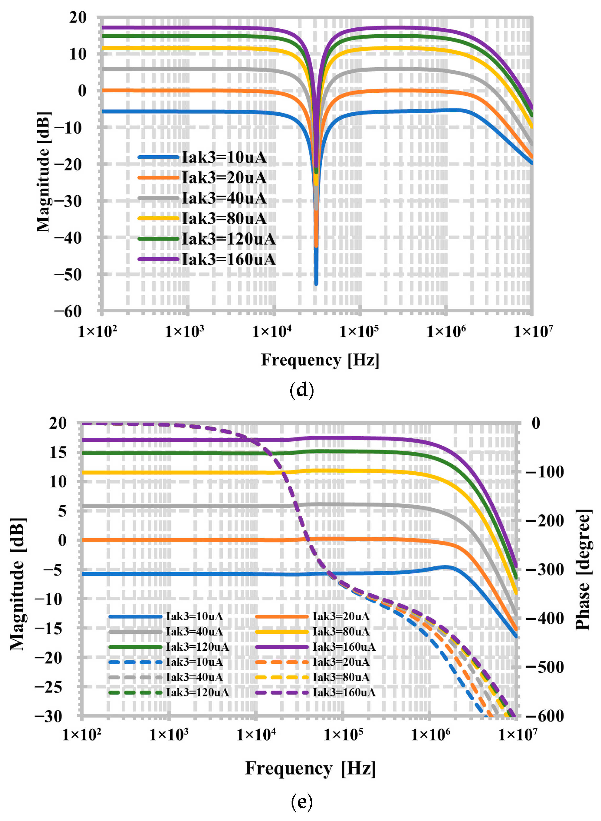
To demonstrate that the current gain of the filters’ transfer functions can be controlled, Figure 12 shows the simulated magnitude frequency responses of the LPF, BPF, HPF, BSF, and APF when the current gain was varied by the biasing current (10, 20, 40, 80, 120, and 160 μA), and the biasing current was fixed as 20 μA. The maximum power consumption ( = 160 μA) was 3.72 mW.
Figure 12.
Simulated magnitude frequency responses of the (a) LPF, (b) HPF, (c) BPF, (d) BSF, and magnitude and phase frequency responses of the (e) APF, with different gains.
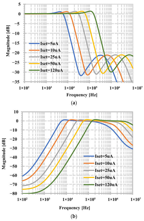
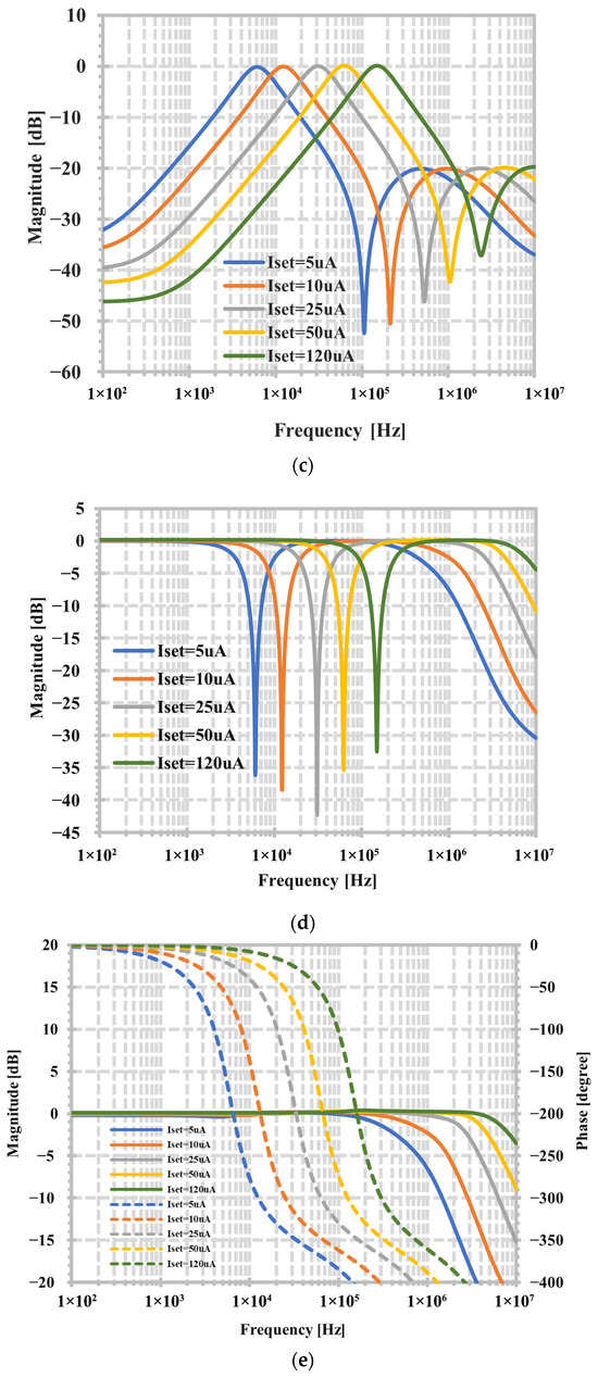
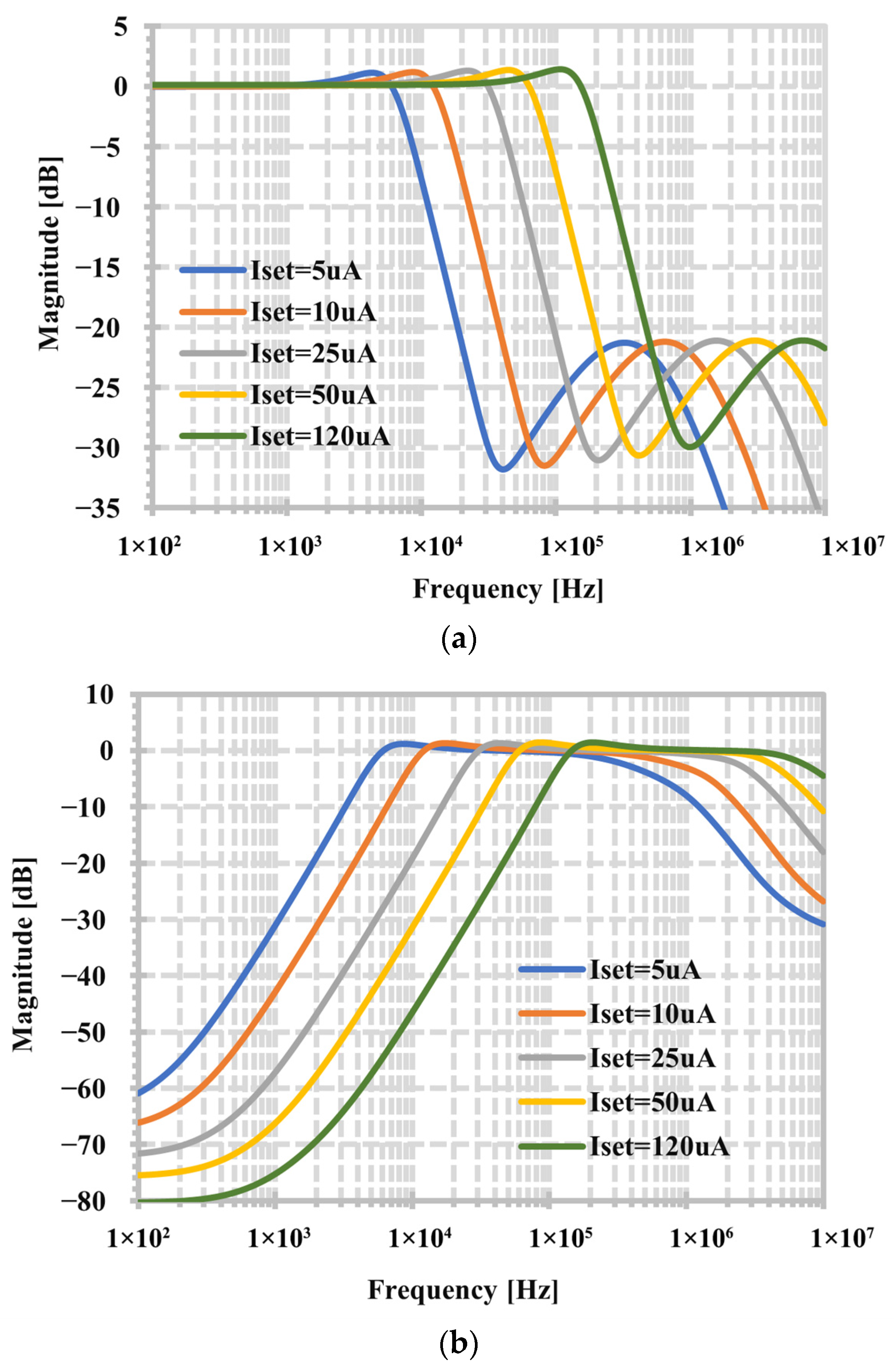
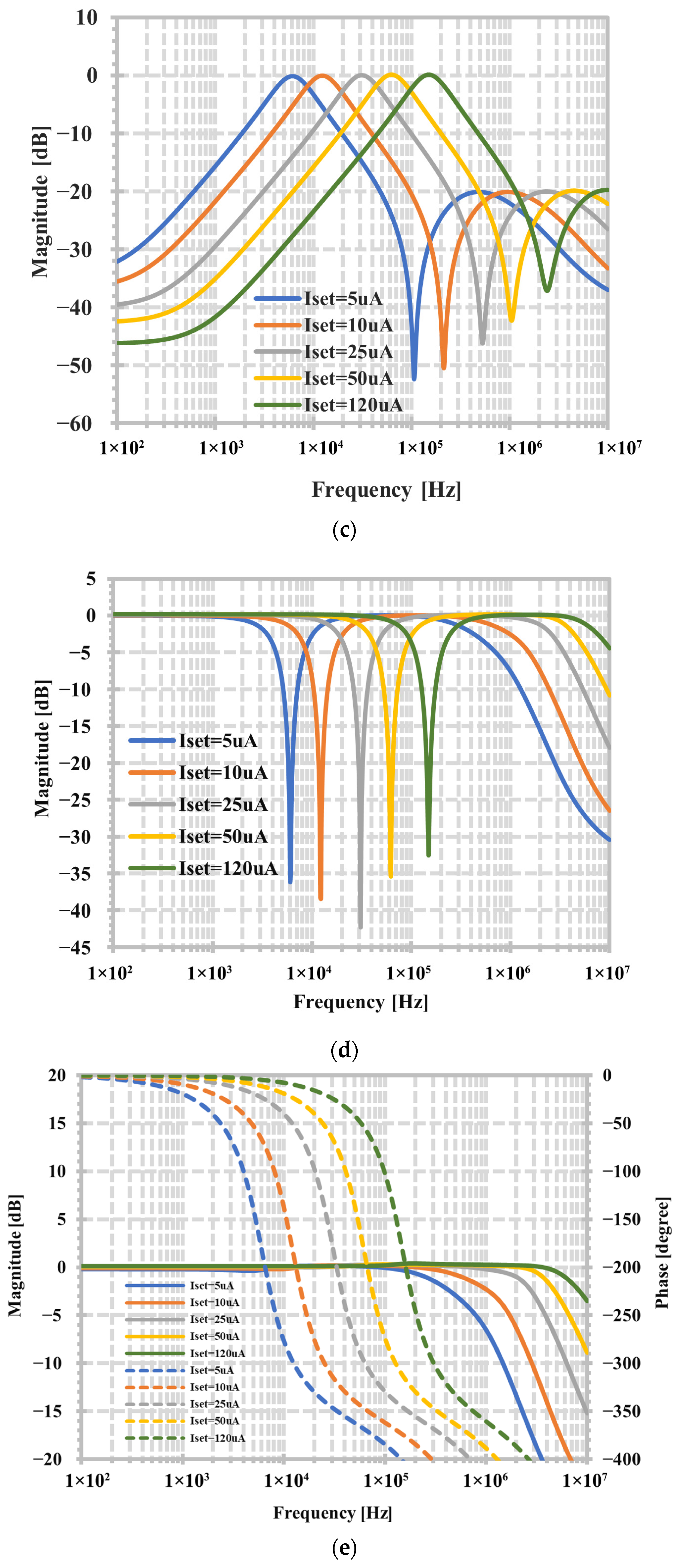
Figure 13 shows the simulated magnitude frequency responses of the LPF, BPF, HPF, BSF, and APF when the biasing current was varied. When was set to [5, 10, 25, 50, 120] μA, the natural frequencies were [6.09, 12.3, 30.9, 63.37, 149.62] kHz, respectively. For the minimum = 5 μA and the maximum = 120 μA, the power consumptions were [0.47 and 6.37] mW, respectively.
Figure 13.
Magnitude frequency responses of the (a) LPF, (b) HPF, (c) BPF, (d) BSF, and magnitude and phase frequency responses of the (e) APF, with a different biasing current .
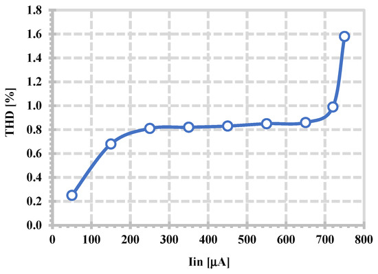
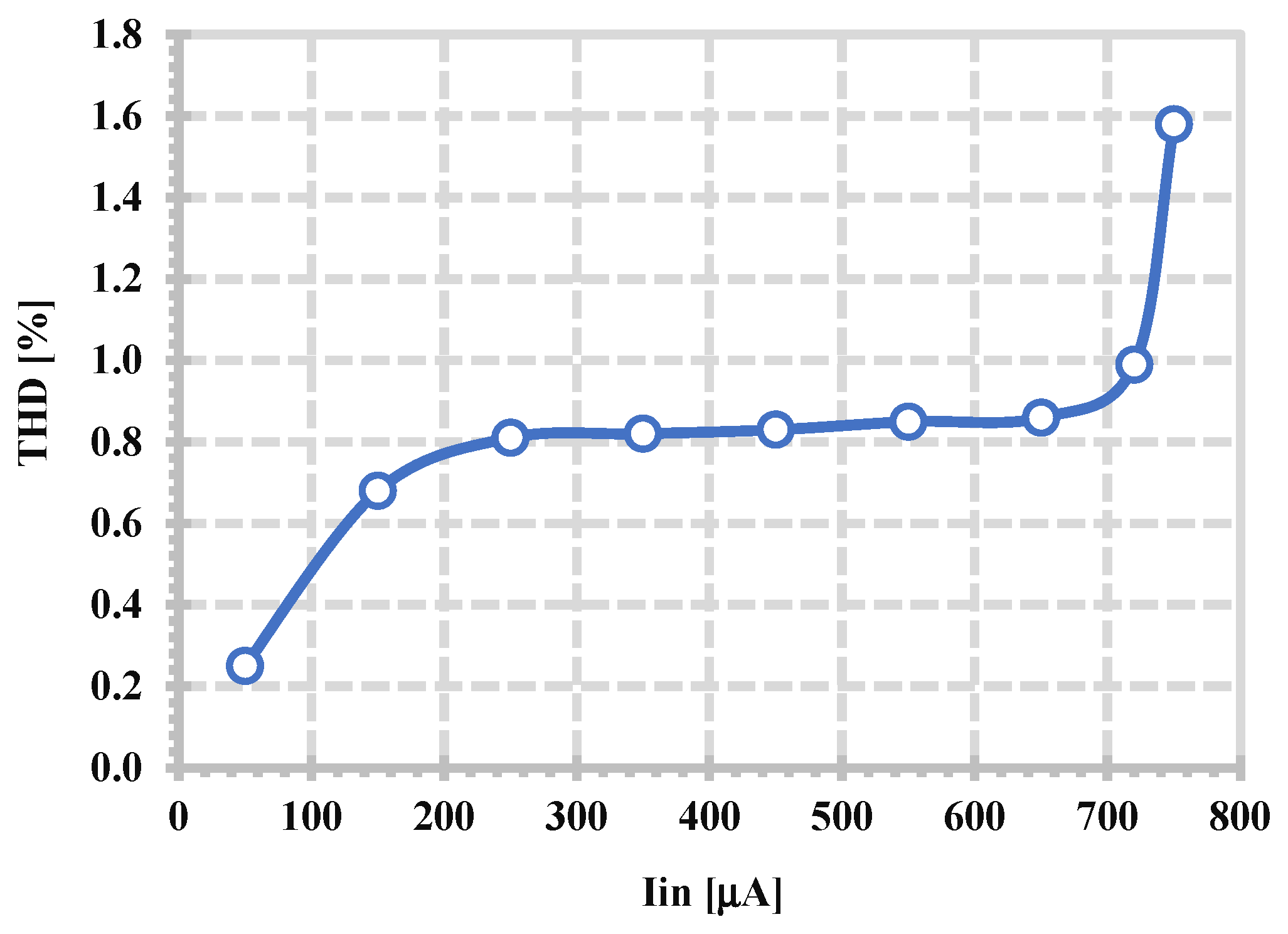
Figure 14 shows the simulated total harmonic distortion (THD) of the LPF when the input frequency of 1 kHz was applied, and the input amplitude was varied. For a THD of 1%, the input amplitude was 720 μA.
Figure 14.
THD of the LPF with a different amplitude of the input current and 1.
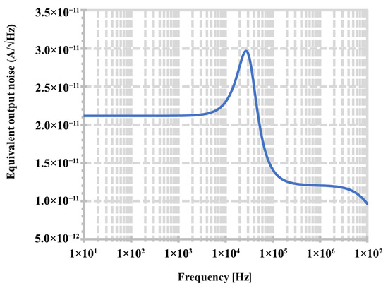
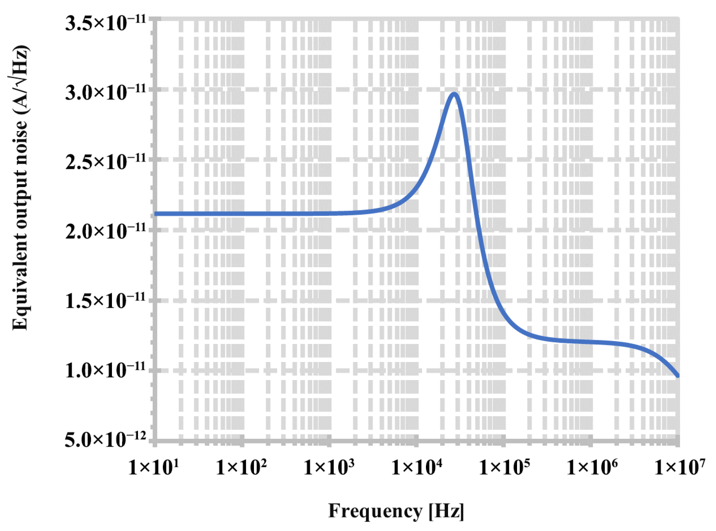
Figure 15 shows the equivalent output current noise of the LPF, which can be used to evaluate the dynamic range (DR) of the filter. For the bandwidth of 30.9 kHz, the integrated output noise was calculated to be 4.45 nA, giving a dynamic range (DR) of 101.16 dB.
Figure 15.
The equivalent output current noise of the LPF.
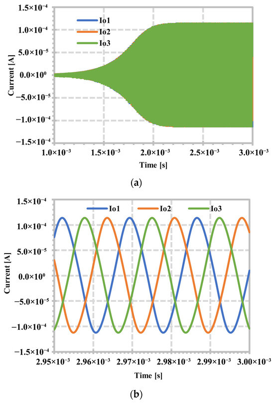
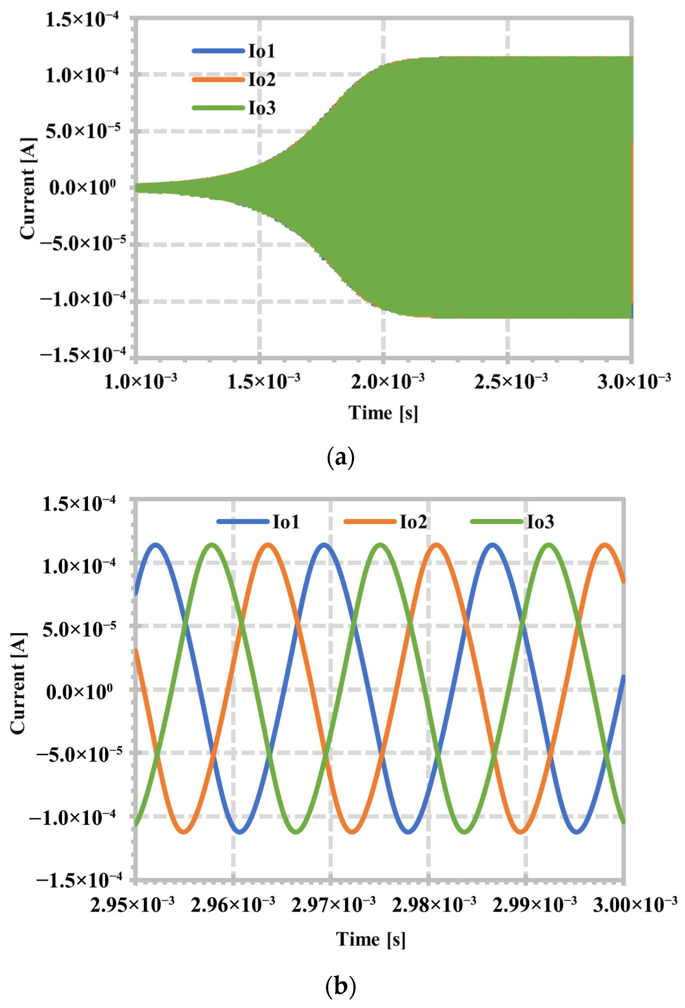
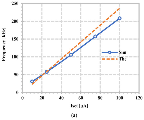
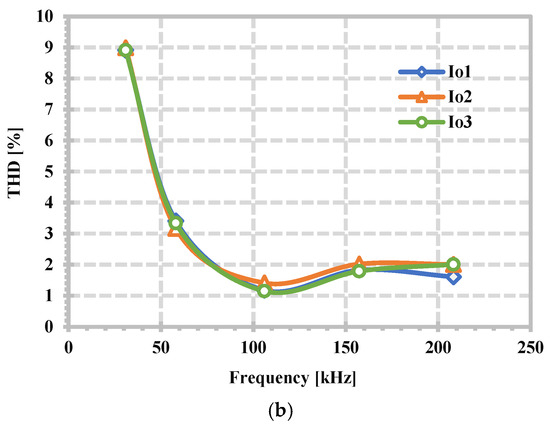
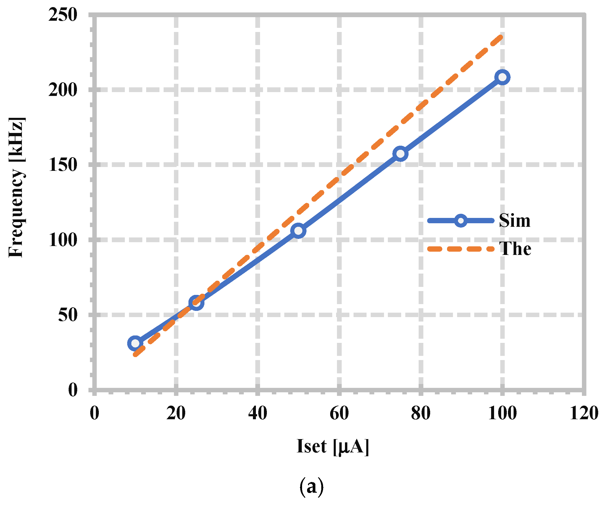
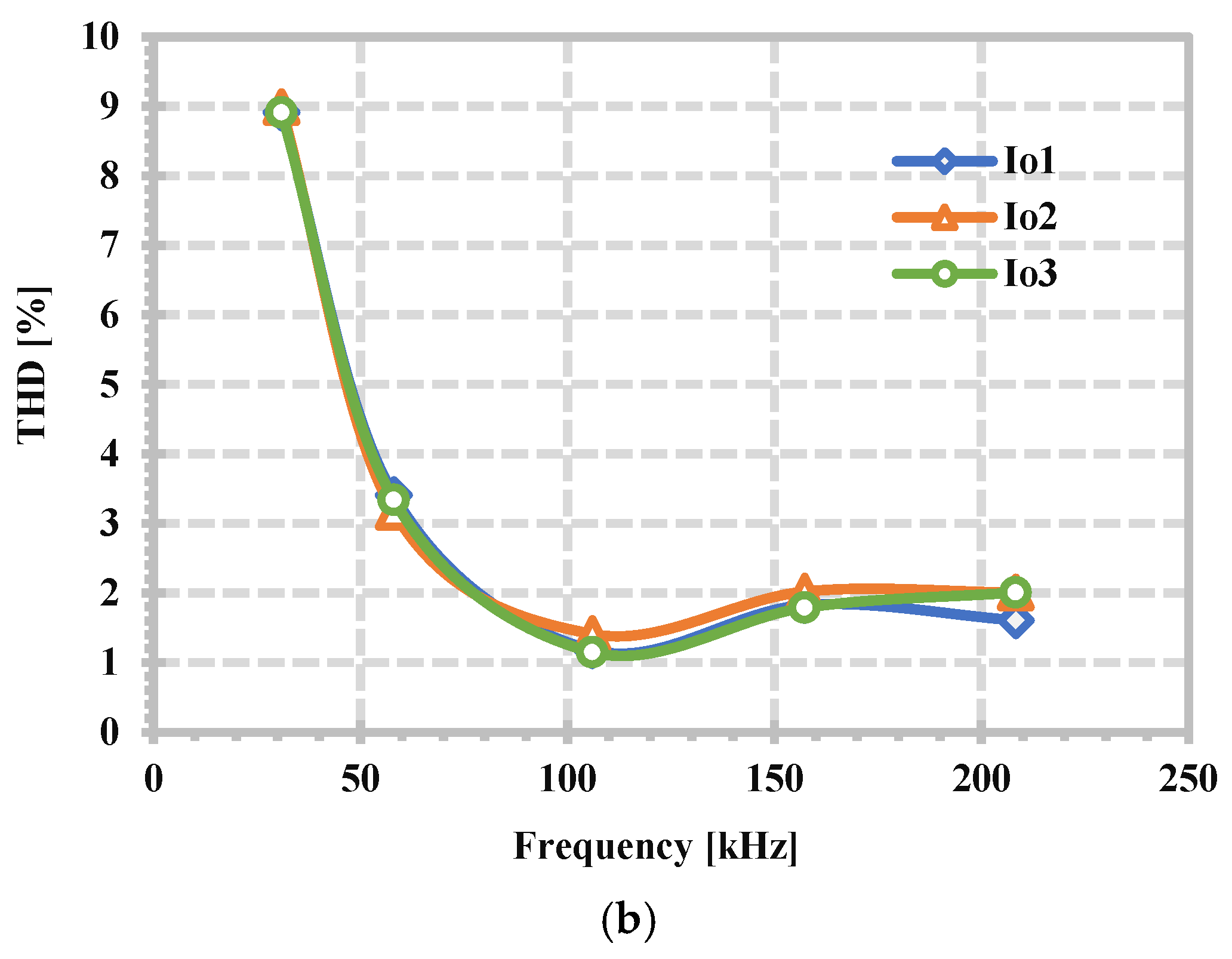
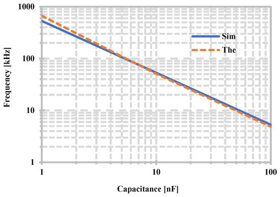
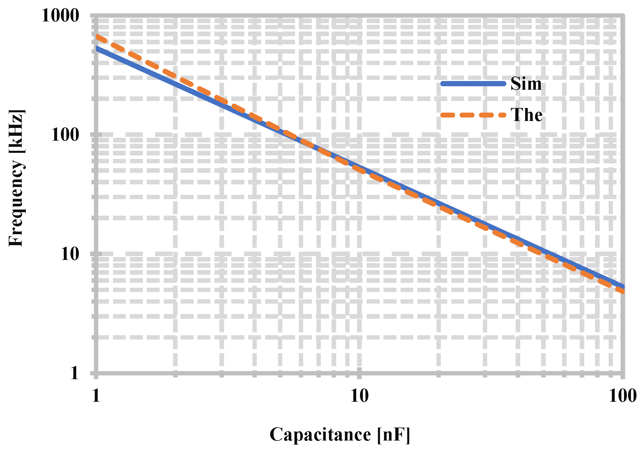
The proposed three-phase sinusoidal oscillator was also simulated. The capacitance value of 9 nF was used. Figure 16 shows the simulated output waveforms of the three-phase sinusoidal oscillator when the biasing currents = 25 µA and 20 µA, and the biasing current was used to control the condition of oscillation ( 40 µA). The circuit generated 58 kHz of oscillating frequency. Figure 17a shows the simulated oscillating frequency when the setting current was varied. The circuit generated frequencies from 30.9 to 200.8 kHz when was varied from 10 to 108.2 μA. The theoretical value given by (24) was used for comparison. Under the same conditions used to obtain the result in Figure 17a, the THD of the output signals was investigated and is shown in Figure 17b. Figure 18 illustrates the oscillating frequencies when the capacitance value () was varied. The theoretical value by (24) was also used for comparison.
Figure 16.
Simulated output waveform of the three-phase oscillator, (a) the starting oscillation, and (b) the steady state.
Figure 17.
(a) Variation of the oscillating frequency with different biasing currents , (b) THD of output signals.
Figure 18.
Variation of the oscillating frequency with different capacitances.
3.2. Experimental Results
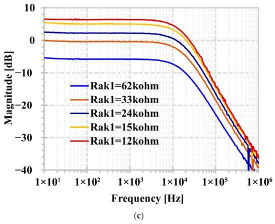
The proposed EX-CCCII was realized using commercially available bipolar junction transistors, namely the 2N3904 (NPN) and 2N3906 (PNP) types. The EX-CCCII operates with a ±1.2 V supply. The bias current is defined by a 24 kΩ resistor. Similarly, the bias currents and (for 1, 2, 3) are established by appropriate resistor values to control the current gain. The current is fixed by a 33 kΩ resistor (), whereas the bias current , which governs the current gain of the EX-CCCII, is configured through suitable resistor values ().
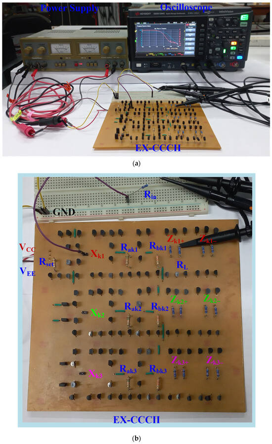
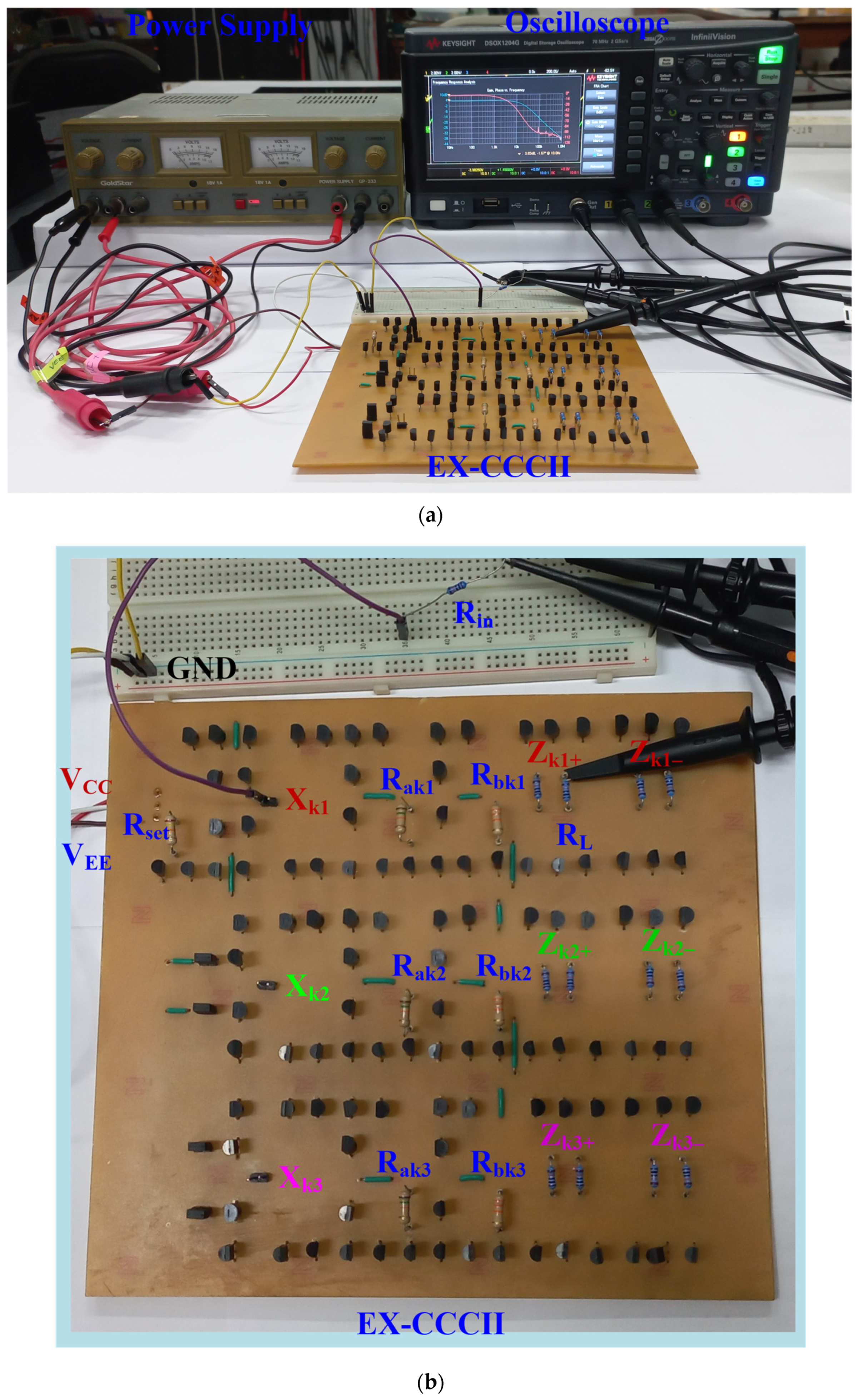
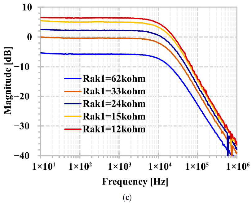
Figure 19a,b shows the implementation of EX-CCCII. To test the frequency response, a KEYSIGHT DSOX1204G oscilloscope was used both to supply the sinusoidal input signal and to measure the output waveforms. A 100 kΩ resistor () is used to convert the voltage input signal into a current, while another 100 kΩ resistor () is employed to convert the current output signal into a voltage. The measured frequency responses corresponding to the values of 65 kΩ, 33 kΩ, 24 kΩ, 15 kΩ, and 12 kΩ are shown in Figure 19c.
Figure 19.
Experimental implementation of the EX-CCCII: (a) test setup, (b) close-up view of the EX-CCCII, and (c) measured frequency responses for different current gain values.
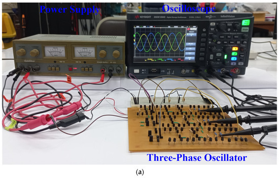
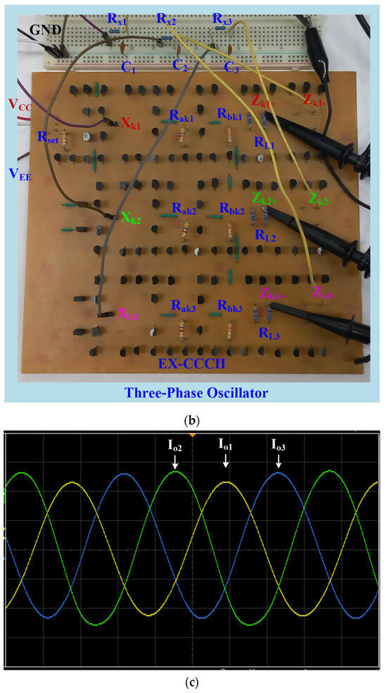
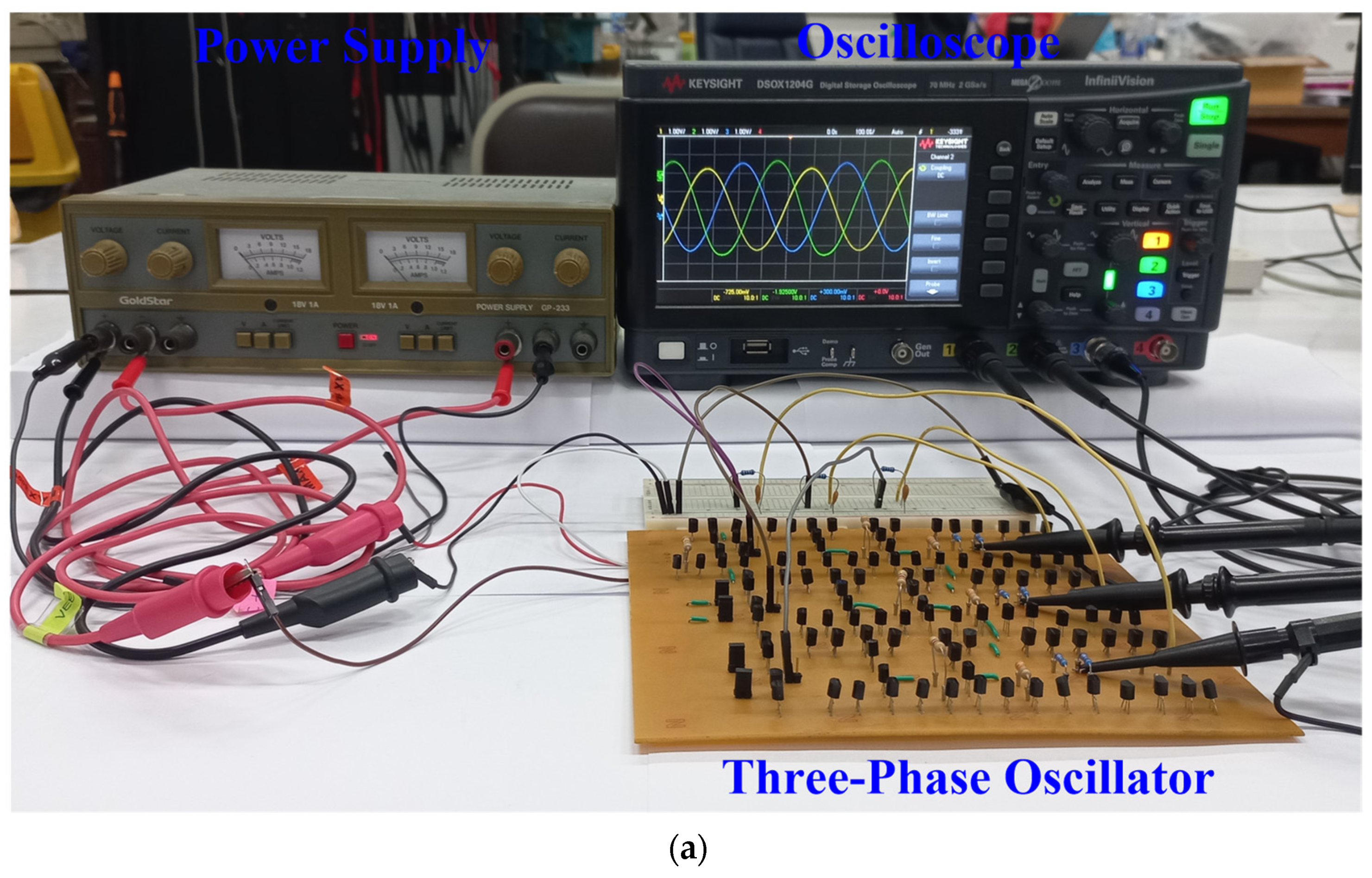
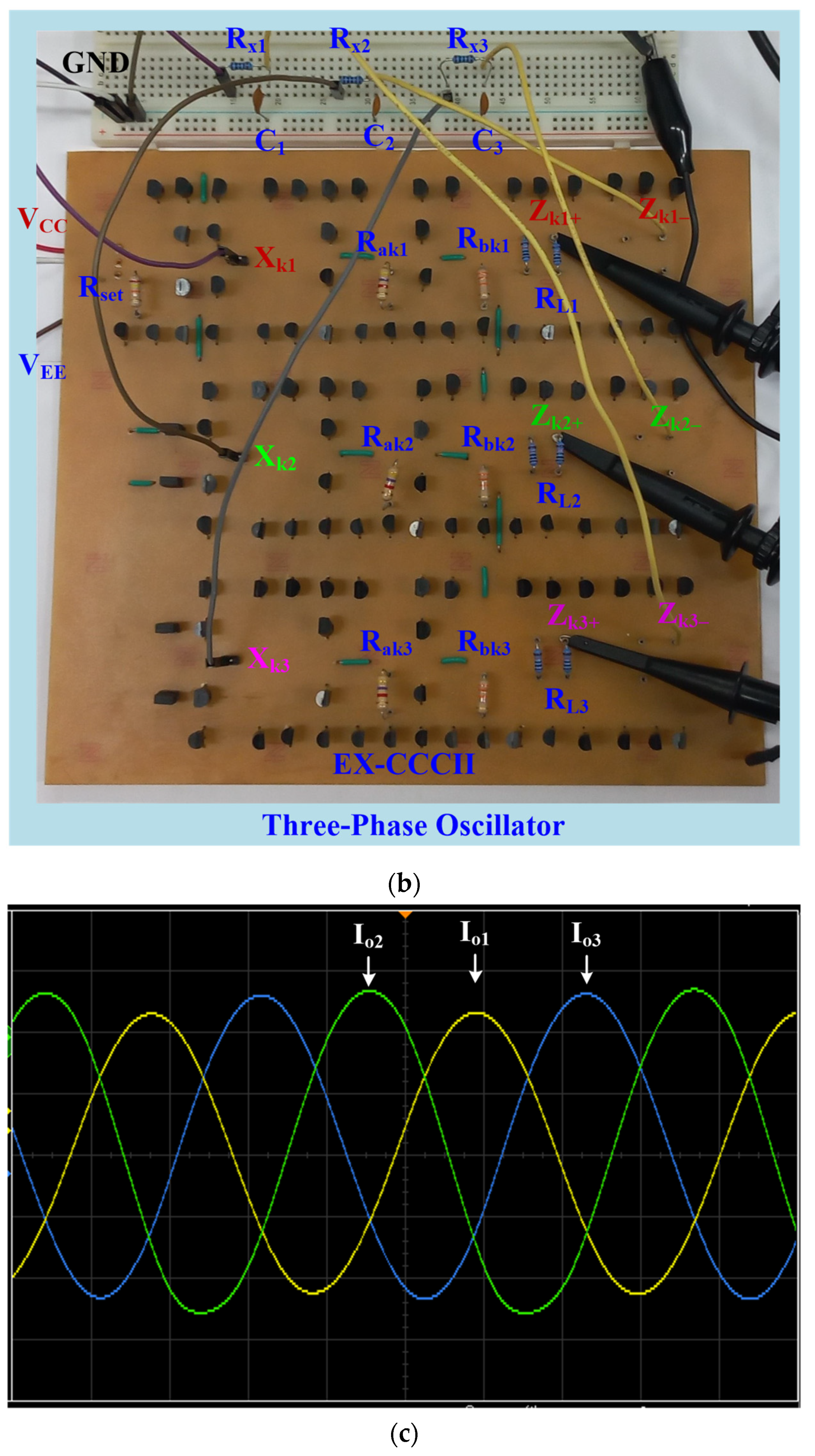
To validate and demonstrate its practical functionality, the EX-CCCII was implemented in a three-phase oscillator, as illustrated in Figure 20a,b. In this study, the condition of oscillation in the oscillator is controlled by adjusting the current gain of the EX-CCCII. The resistors (for = 1, 2, 3) of EX-CCCII are set to 10 kΩ, and the capacitors , , and are chosen to be 10 nF. The output currents , , and are converted to voltages using resistor values of 100 kΩ. The measured output waveform of a three-phase oscillator is shown in Figure 20c. The circuit produced an output frequency of 2.55 kHz, with each phase equally spaced, which is consistent with the theoretical analysis.
Figure 20.
Experimental application of the EX-CCCII in a three-phase oscillator: (a) test setup, (b) zoomed-in view of the oscillator, and (c) measured output waveform.
However, since the proposed circuit has not yet been fabricated in integrated circuit form, the simulations were performed using bipolar parameters corresponding to an integrated circuit implementation, whereas the experimental results were obtained using discrete components (e.g., 2N3900 and 2N3600 transistors, resistors, and capacitors). Due to this difference, some deviations between the simulated and experimental results are expected. Nevertheless, the experimental results are primarily used to confirm the fundamental operation and feasibility of the proposed EX-CCCII with a controlled current gain, and they exhibit consistent trends with the simulation results. Therefore, although the experimental setup may not fully verify all performance parameters of the EX-CCCII with the controlled current gain and the oscillator, it provides practical validation of the circuit functionality.
The proposed EX-CCCII with a controlled current gain is compared to previously reported works in [40,41,42], as summarized in Table 3. The circuits in [40,41,42] provide only a single output current gain. Therefore, they employ fewer active transistors. In contrast, the proposed circuit employs 67 active transistors to realize three output current gains. The circuit in [42] provides a high-performance current conveyor with high current gain accuracy. Although it achieves a higher current gain accuracy than the proposed circuit, the proposed BJT-based implementation offers a wider tunable range compared to the CMOS-based circuits, limited by the square-law characteristic. This wider tunability provides greater design flexibility in practical applications, partially compensating for the reduced current gain accuracy.
Table 3.
Comparison of the proposed circuit with selected previous works.
4. Conclusions
This paper presents a novel EX-CCCII with controlled current gain. For this EX-CCCII, the current gain between the - and -terminals is available, and the parasitic resistance at the -terminals is provided. Both current gain and parasitic resistance can be electronically controlled. To highlight the benefits of the proposed EX-CCCII with the controlled current gain, it was used to implement a current-mode universal filter and a current-mode three-phase sinusoidal oscillator. The applications show that the current gain of the EX-CCCII can be used to adjust the current gain of the filters’ transfer functions and the oscillator’s condition of oscillation. The natural frequency of the universal filter and the frequency of oscillation of the oscillator can be electronically controlled. The simulation results validate the functionality and the benefits of the proposed circuit and its applications. Furthermore, the experimental results of the EX-CCCII, along with its application in the three-phase oscillator, provide additional validation of the concept and confirm its practical functionality. Although a single EX-CCCII with controlled current gain can be used to realize a universal filter or a three-phase oscillator, its internal structure consists of numerous bipolar transistors. As a result, adjusting the bias currents to achieve the desired current gain is difficult in practice. However, this limitation can be alleviated when the circuit is implemented in integrated circuit form.
Author Contributions
Conceptualization, S.T., M.K., and F.K.; methodology, T.K., F.K., and M.K.; software, F.K. and M.K.; validation, M.K. and F.K.; formal analysis, F.K., T.K., and M.K.; investigation, F.K., T.K., T.N., and M.K.; resources, S.T., T.N., and M.K.; data curation, F.K., J.V., and M.K.; writing—original draft preparation, F.K. and M.K.; writing—review and editing, F.K. and M.K.; visualization, F.K. and M.K.; supervision, F.K. and M.K.; project administration, F.K. and M.K.; funding acquisition, S.T. All authors have read and agreed to the published version of the manuscript.
Funding
This research received no external funding.
Institutional Review Board Statement
Not applicable.
Informed Consent Statement
Not applicable.
Data Availability Statement
Dataset available on request from the authors.
Acknowledgments
This work was supported in part by the School of Engineering, King Mongkut’s Institute of Technology Ladkrabang, under Grant 2568-02-01-022, and in part by the University of Defence, Brno, within the Organization Development Project VAROPS.
Conflicts of Interest
The authors declare no conflicts of interest.
References
- Sedra, A.; Smith, K. A Second-Generation Current Conveyor and Its Applications. IEEE Trans. Circuit Theory 1970, 17, 132–134. [Google Scholar] [CrossRef] [Scilit]
- Senani, R.; Bhaskar, R.R.; Singh, A.K. Current Conveyors: Variant Applications and Hardware Implementations; Springer: Berlin/Heidelberg, Germany, 2015. [Google Scholar]
- Wilson, B. Analogue Current Mode Circuits. Int. J. Electr. Eng. Educ. 1989, 26, 206–223. [Google Scholar] [CrossRef] [Scilit]
- Toumazou, C.; Lidgey, F.J.; Haig, D.G. Analogue IC Design: The Current-Mode Approach, London, Peter Peregrinus; Presbyterian Publishing Corp: Louisville, KY, USA, 1990. [Google Scholar]
- Elwan, H.O.; Soliman, A.M. Novel CMOS Differential Voltage Current Conveyor and Its Application. IEE Proc.-Circuits Devices Syst. 1997, 144, 195–200. [Google Scholar] [CrossRef] [Scilit]
- Chiu, W.; Liu, S.-I.; Tsao, H.-W.; Chen, J.-J. CMOS Differential Difference Current Conveyors and Their Applications. IEE Proc.-Circuits Devices Syst. 1996, 143, 91–96. [Google Scholar] [CrossRef] [Scilit]
- El-Adawy, A.A.; Soliman, A.M.; Elwan, H.O. A Novel Fully Differential Current Conveyor and Applications for Analog VLSI. IEEE Trans. Circuits Syst.-II 2000, 47, 306–313. [Google Scholar] [CrossRef] [Scilit]
- Kacar, F.; Metin, B.; Kuntman, H. A New CMOS Dual-X Second Generation Current Conveyor (DXCCII) with an FDNR Circuit Application. AEU-Int. J. Electron. Commun. 2010, 64, 774–778. [Google Scholar] [CrossRef] [Scilit]
- Maheshwari, S. Realization of Simple Electronic Functions Using EXCCII. J. Circuits Syst. Comput. 2017, 26, 1750171. [Google Scholar] [CrossRef] [Scilit]
- Maheshwari, S.; Agrawal, D. High Performance Voltage-Mode Tunable All-Pass section. J. Circuits Syst. Comput. 2015, 24, 1550082. [Google Scholar] [CrossRef] [Scilit]
- Maheshwari, S. Current Conveyor All-Pass Sections: Brief Review and Novel Solution. Sci. World J. 2013, 2013, 429391. [Google Scholar] [CrossRef] [Scilit]
- Maheshwari, S. Tuning Approach for First-Order Filters and New Current-Mode Circuit Example. IET Circuits Devices Syst. 2018, 12, 478–485. [Google Scholar] [CrossRef] [Scilit]
- Maheshwari, S. Voltage-Mode Full-Wave Precision Rectifier and an Extended Application as ASK/BPSK Circuit Using a Single EXCCII. Int. J. Electron. Commun. 2018, 84, 234–241. [Google Scholar] [CrossRef] [Scilit]
- Agrawal, D.; Maheshwari, S. Current-Mode Precision Full-Wave Rectifier Circuits. Circuits Syst. Signal Process. 2017, 36, 4293–4308. [Google Scholar] [CrossRef] [Scilit]
- Das, R.; Paul, S.K. Resistorless Current Mode Precision Rectifier Using EXCCII. Analog. Integr. Circuits Signal Process. 2020, 103, 511–522. [Google Scholar] [CrossRef] [Scilit]
- Kumar, A. Single EXCCII-Based Analog Multiplier Structure. J. Circuits Syst. Comput. 2021, 30, 2150107. [Google Scholar] [CrossRef] [Scilit]
- George, M.A.; Bhavani, D.; Kamath, D.V. EX-CCII Based FOPID Controller for Electric Vehicle Speed Control. In IEEE International Conference on Distributed Computing, VLSI, Electrical Circuits and Robotics (DISCOVER), India; IEEE: New York, NY, USA, 2020; pp. 47–51. [Google Scholar] [CrossRef] [Scilit]
- Chaturvedi, B.; Kumar, A. Single EXCCII Based Square/Triangular Wave Generator for Capacitive Sensor Interfacing and Brief Review. In VLSI and Post-CMOS Electronics: Devices, Circuits and Interconnects; IET: London, UK, 2019; Volume 2, pp. 329–349. [Google Scholar] [CrossRef] [Scilit]
- Kapoulea, S.; Psychalinos, C.; Elwakil, A.S. Single Active Element Implementation of Fractional-Order Differentiators and Integrators. Int. J. Electron. Commun. 2018, 97, 6–15. [Google Scholar] [CrossRef] [Scilit]
- Joshana, R.; Singh, Y.S.; Ranjan, A. An Electronically Tunable Fractional Order Inductor Employing VD-EXCCII. Int. J. Electron. Commun. 2023, 174, 155055. [Google Scholar] [CrossRef] [Scilit]
- Faseehuddin, M.; Herencsar, N.; Albrni, M.A.; Sampe, J. Electronically Tunable Mixed-Mode Universal Filter Employing a Single Active Block and a Minimum Number of Passive Components. Appl. Sci. 2021, 11, 55. [Google Scholar] [CrossRef] [Scilit]
- Maheshwari, S.; Agrawal, D. Cascadable and Tunable Analog Building Blocks Using EX-CCCII. J. Circuits Syst. Comput. 2017, 26, 1750093. [Google Scholar] [CrossRef] [Scilit]
- Agrawal, D.; Maheshwari, S. Cascadable Current Mode Instrumentation Amplifier. AEU-Int. J. Electron. Commun. 2018, 94, 91–101. [Google Scholar] [CrossRef] [Scilit]
- Singh, P.; Nagaria, R.K. Single EX-CCCII Based Electronically Tunable Current Mode Instrumentation Amplifier. Eng. Rev. 2022, 42, 1–16. [Google Scholar] [CrossRef] [Scilit]
- Singh, P.; Nagaria, R.K. Low Voltage EX-CCCII Based on Quasi-Floating Gate Technique and its Application as Precision Rectifier. Int. J. Electron. Commun. 2022, 155, 154378. [Google Scholar] [CrossRef] [Scilit]
- Agrawal, D.; Maheshwari, S. Electronically Tunable Grounded Immittance Simulators Using an EX-CCCII. Int. J. Electron. 2020, 107, 1625–1648. [Google Scholar] [CrossRef] [Scilit]
- Singh, P.; Varshney, V.; Kumar, A.; Nagaria, R.K. DV-EXCCCII-Based Electronically Tunable Voltage Mode All-Pass Filter. In Recent Trends in Electronics and Communication; Dhawan, A., Tripathi, V.S., Arya, K.V., Naik, K., Eds.; Lecture Notes in Electrical Engineering; Springer: Singapore, 2022; Volume 777. [Google Scholar] [CrossRef] [Scilit]
- Agrawal, D.; Maheshwari, S. Current Mode Filters With Reduced Complexity Using a Single EX-CCCII. Int. J. Electron. Commun. 2017, 80, 86–93. [Google Scholar] [CrossRef] [Scilit]
- Singh, P.; Nagaria, R.K. Electronically Tunable DV-EXCCCII-Based Universal Filter. Int. J. Electron. Lett. 2020, 9, 301–317. [Google Scholar] [CrossRef] [Scilit]
- Agrawal, D.; Maheshwari, S. High-Performance Electronically Tunable Analog Filter Using a Single EX-CCCII. Circuits Syst. Signal Process. 2021, 40, 1127–1151. [Google Scholar] [CrossRef] [Scilit]
- Agrawal, D.; Maheshwari, S. Electronically Tunable Mixed-Mode Third-Order Universal Filter Using a Single EX-CCCII. Aust. J. Electr. Electron. Eng. 2022, 19, 307–323. [Google Scholar] [CrossRef] [Scilit]
- Singh, P.; Nagaria, R.K. DV-EXCCCII Based Resistor-Less Current-Mode Universal Biquadratic Filter. Adv. Technol. Innov. 2023, 8, 12–28. [Google Scholar] [CrossRef] [Scilit]
- Kumngern, M.; Khateb, F.; Kulej, T.; Tooprakai, S. Current-Mode Active Filter Using EX-CCCII. Electronics 2024, 13, 2059. [Google Scholar] [CrossRef] [Scilit]
- Agrawal, D.; Tripathi, S.K.; Reddy, N.S.; Reddy, S.V.; Shoaib, M. Design a Configurable First Order Universal Filter Using a Single EX-CCCII. Russ. Microelectron. 2024, 53, 290–296. [Google Scholar] [CrossRef] [Scilit]
- Bhatt, V.; Ranjan, A.; Singh, Y.S. Resistorless Chua’s Diode Implementation for Chaotic Oscillation Employing Single EXCCCII. Int. J. Electron. Commun. 2022, 156, 154398. [Google Scholar] [CrossRef] [Scilit]
- Li, Y.; Hou, J. Pathological Models of EXCCCII and its Applications in Oscillator Synthesis. Wuhan Univ. J. Nat. Sci. 2021, 26, 115–122. [Google Scholar]
- Banerjee, K.; Joshi, M.; Sarkar, C.; Biring, S. Low-Frequency Resistorless Electronically Tunable Quadrature Oscillator Based on an EX-CCCII. J. Electron. Mater. 2023, 52, 3510–3515. [Google Scholar] [CrossRef] [Scilit]
- Senani, R. Novel circuit implementation of current conveyors using an O.A. and an O.T.A. Electron. Lett. 1980, 16, 2–3. [Google Scholar] [CrossRef] [Scilit]
- Knobnob, B. Electronically tunable differential difference current conveyor using commercially available OTAs. J. Circuits Syst. Comput. 2023, 32, 2350295. [Google Scholar] [CrossRef] [Scilit]
- Fabre, A.; Mimeche, N. Class A/AB Second Generation Current Conveyor with Controlled Current Gain. Electron. Lett. 1996, 43, 82–91. [Google Scholar] [CrossRef] [Scilit]
- Surakampontorn, W.; Kumwachara, K. CMOS-Based Electronically Tunable Current Conveyor. Electron. Lett. 1992, 28, 1316–1317. [Google Scholar] [CrossRef] [Scilit]
- Mimaei, S.; Sayin, O.K.; Kuntman, H. A New CMOS Electronically Tunable Current Conveyor and Its Application to Current-Mode Filters. IEEE Trans. Circuits Syst.–I Regul. Pap. 2006, 53, 1448–1458. [Google Scholar] [CrossRef] [Scilit]
- Fabre, A.; Saaid, O.; Wiest, F.; Boucheron, C. High Frequency Applications Based on a New Current Controlled Conveyor. IEEE Trans. Circuits Syst. I Fundam. Theory Appl. 1996, 43, 82–91. [Google Scholar] [CrossRef] [Scilit]
- Kumngern, M.; Chanwutitum, J.; Dejhan, K. Current-Tunable Current-Mode Universal Filter Using Minimum Elements. In 2009 6th International Conference on Electrical Engineering/Electronics, Computer, Telecommunications and Information Technology, Chonburi, Thailand; IEEE: New York, NY, USA, 2009; pp. 582–585. [Google Scholar] [CrossRef] [Scilit]
- Tangsrirat, W.; Tanjaroen, W.; Pukkalanun, T. Current-Mode Multiphase Sinusoidal Oscillator Using CDTA-Based Allpass Sections. AEU-Int. J. Electron. Commun. 2009, 63, 616–622. [Google Scholar] [CrossRef] [Scilit]
- Wu, D.-S.; Liu, S.-I.; Hwang, Y.-S.; Wu, Y.-P. Multiphase Sinusoidal Oscillator Using Second-Generation Current Conveyors. Int. J. Electron. 1995, 78, 645–651. [Google Scholar] [CrossRef] [Scilit]
- Thongdit, P.; Kunto, T.; Prommee, P. OTA high pass filter-based multiphase sinusoidal oscillator. In 2015 38th International Conference on Telecommunications and Signal Processing (TSP), Prague, Czech Republic; IEEE: New York, NY, USA, 2015; pp. 1–5. [Google Scholar] [CrossRef] [Scilit]
- Kumngern, M.; Junnapiya, S.; Dejhan, K. Current-Mode Multiphase Sinusoidal Oscillator Using Translinear Conveyors. In 2009 6th International Conference on Electrical Engineering/Electronics, Computer, Telecommunications and Information Technology, Chonburi, Thailand; IEEE: New York, NY, USA, 2009; pp. 538–541. [Google Scholar] [CrossRef] [Scilit]
- Frey, D.R. Log Domain Filter: An Approach to Current Mode Filtering. IEE Proc. Part G Circuits Devices Syst. 1993, 140, 406–416. [Google Scholar] [CrossRef] [Scilit]

Disclaimer/Publisher’s Note: The statements, opinions and data contained in all publications are solely those of the individual author(s) and contributor(s) and not of MDPI and/or the editor(s). MDPI and/or the editor(s) disclaim responsibility for any injury to people or property resulting from any ideas, methods, instructions or products referred to in the content. |
© 2026 by the authors. Licensee MDPI, Basel, Switzerland. This article is an open access article distributed under the terms and conditions of the Creative Commons Attribution (CC BY) license.