Ka-Band Marchand Balun with Edge- and Broadside-Coupled Hybrid Configuration


Abstract
:1. Introduction
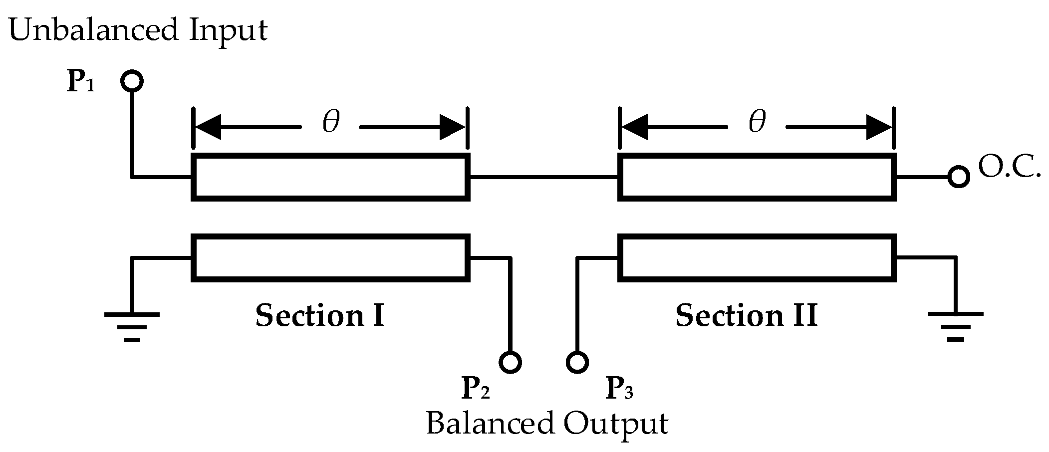
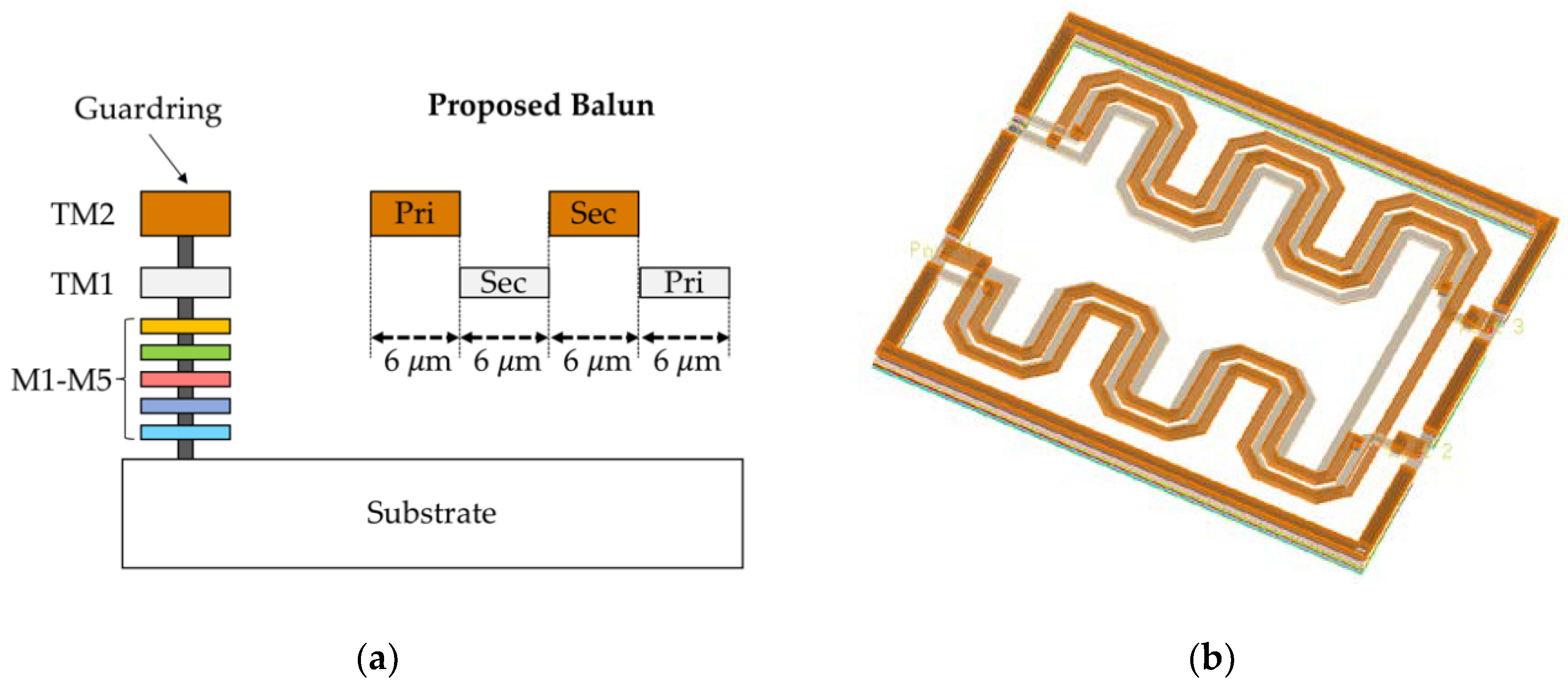
2. Design of the Proposed Balun
2.1. Technology
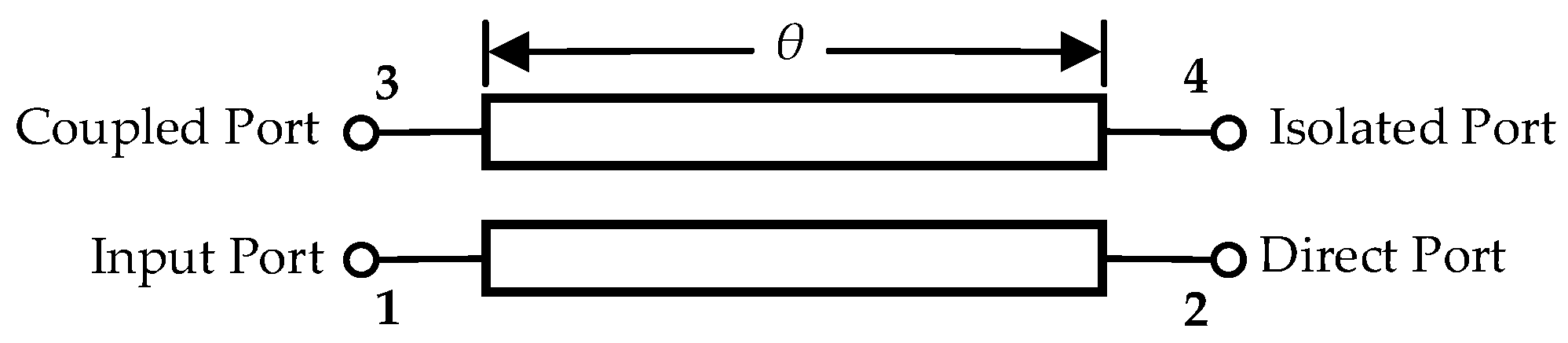
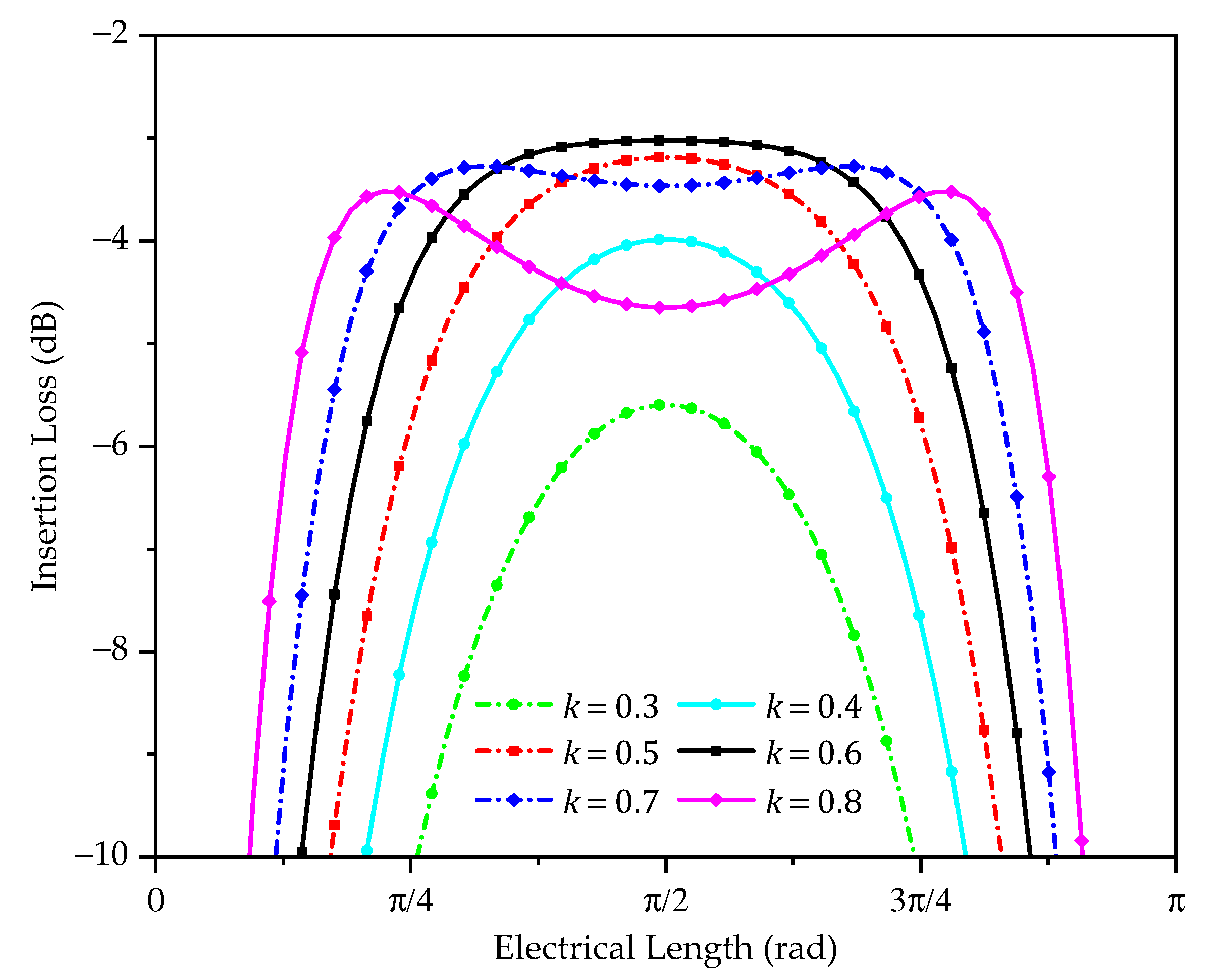
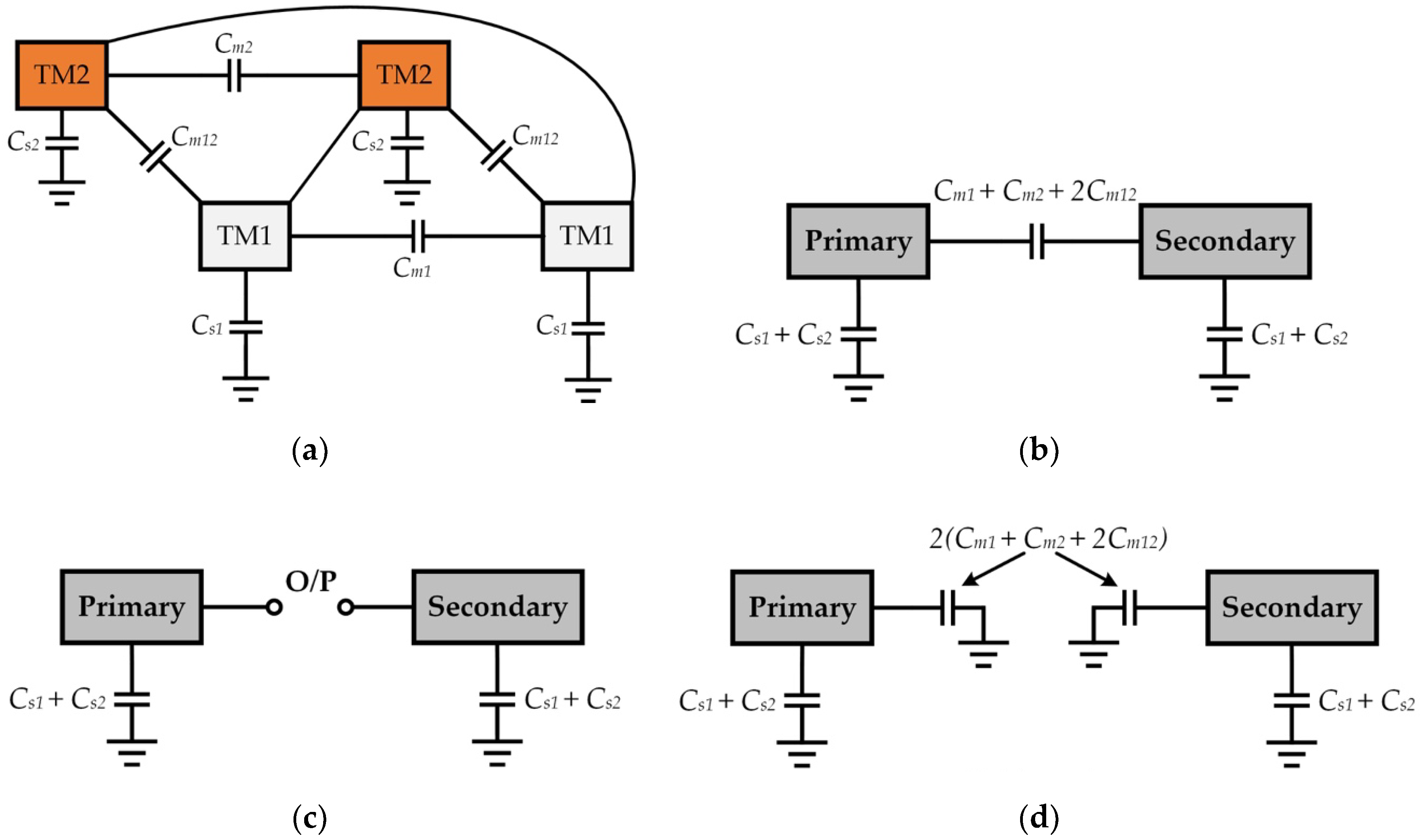
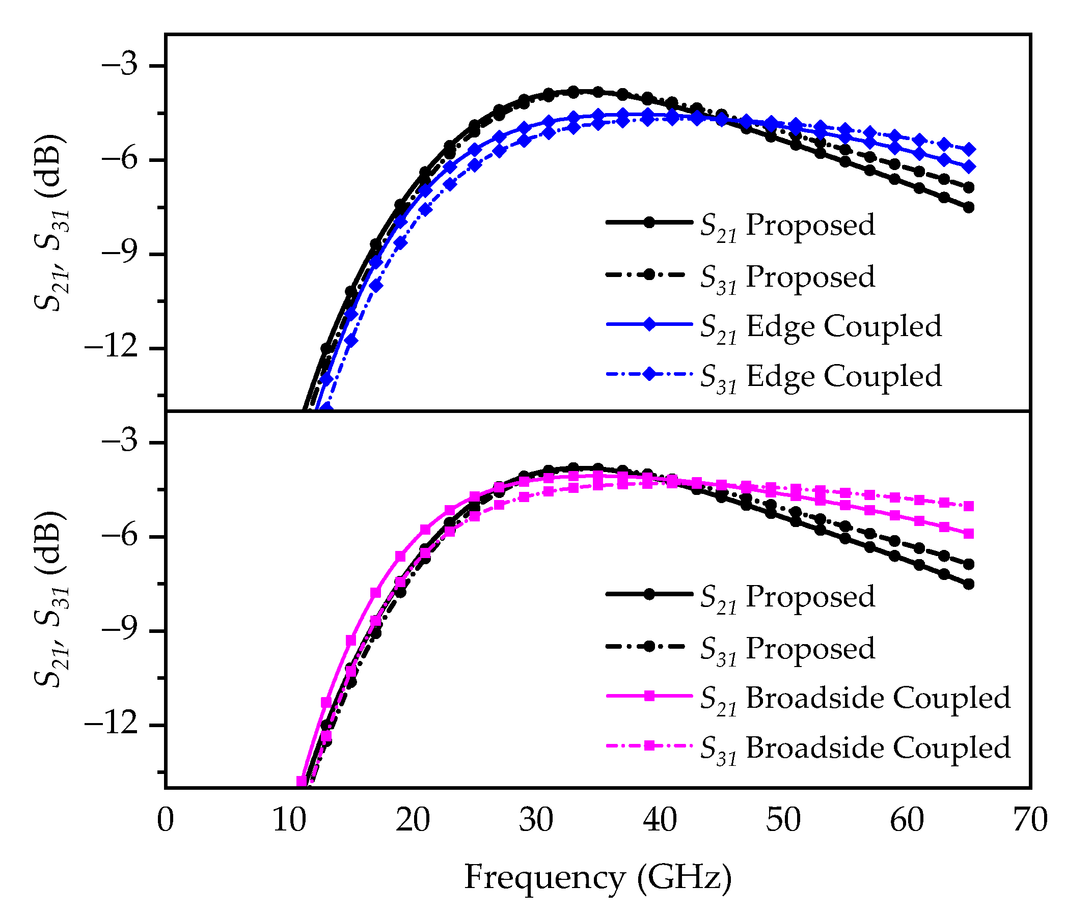
2.2. Balun Analysis
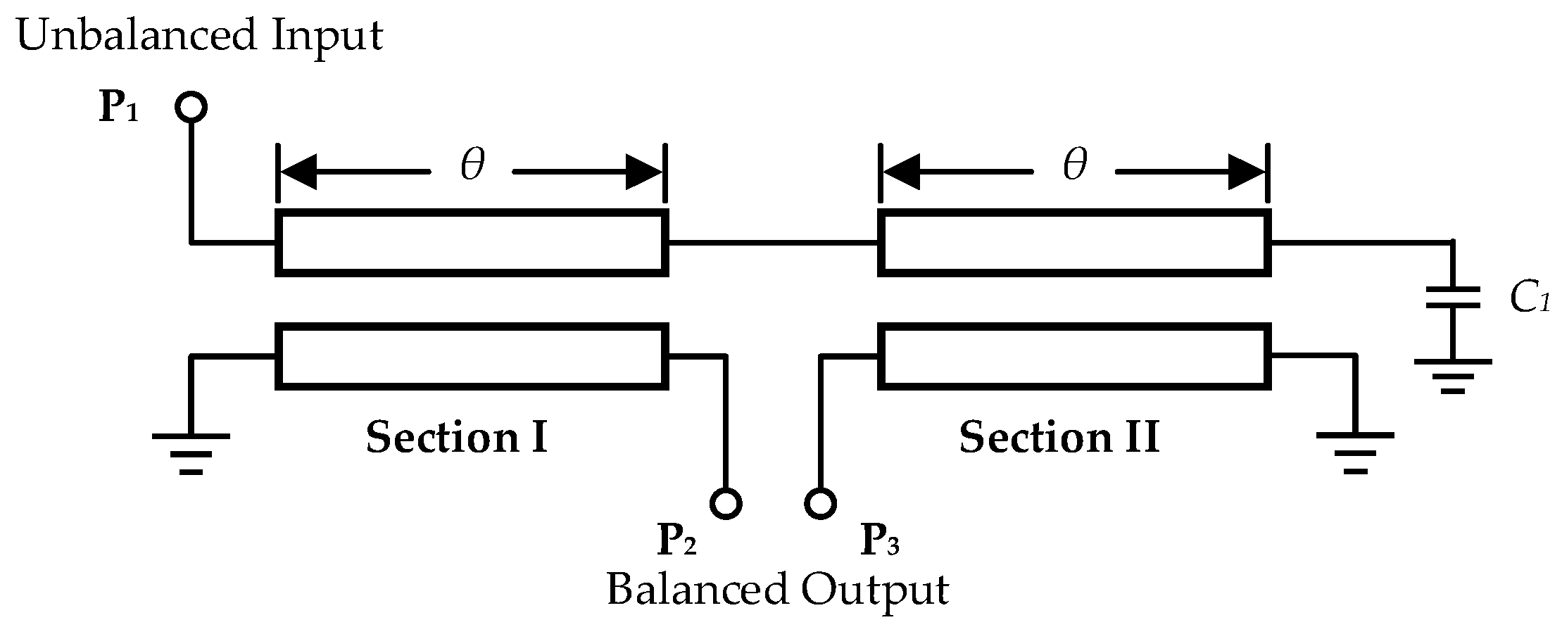
2.3. Proposed Balun
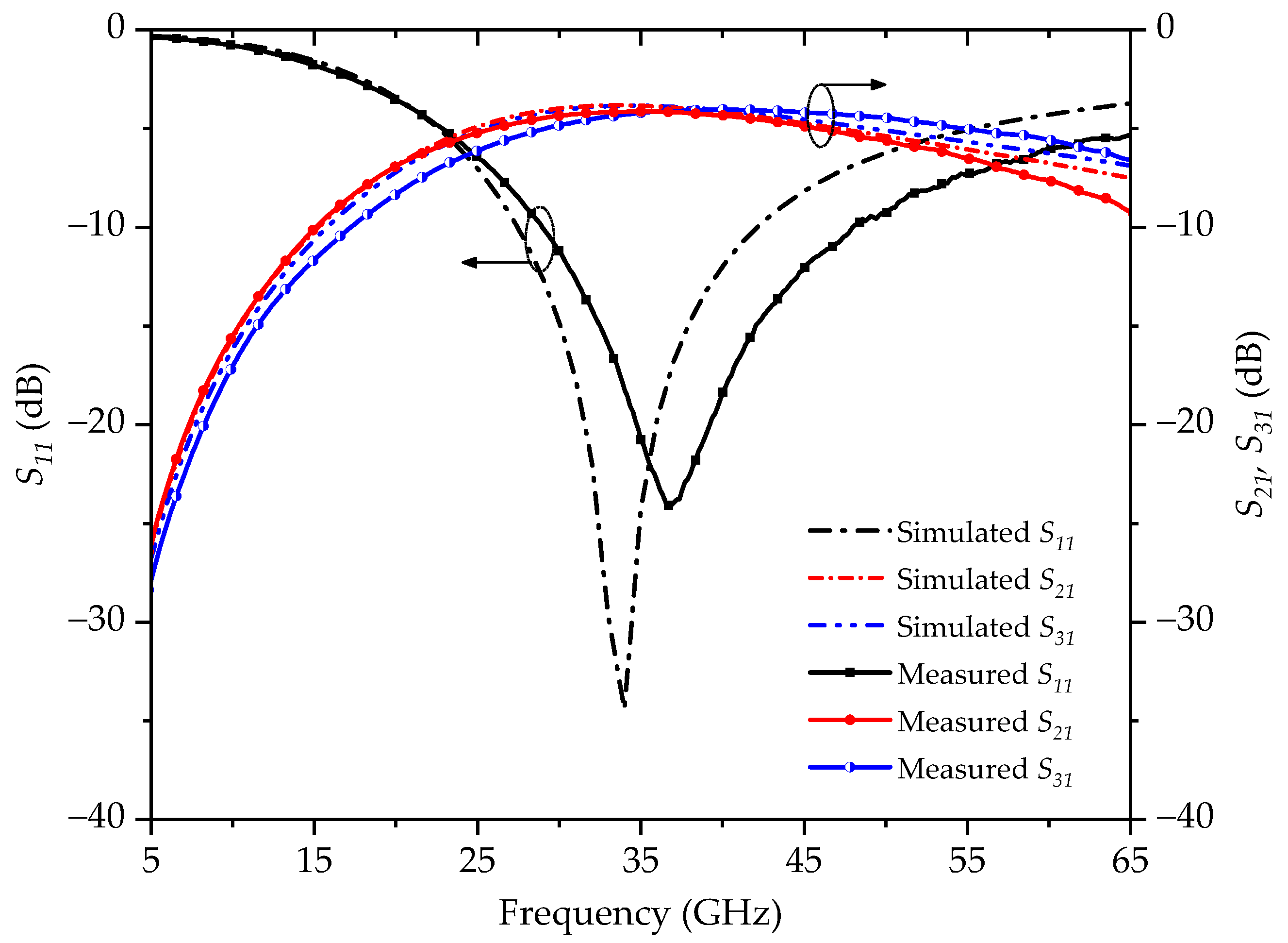
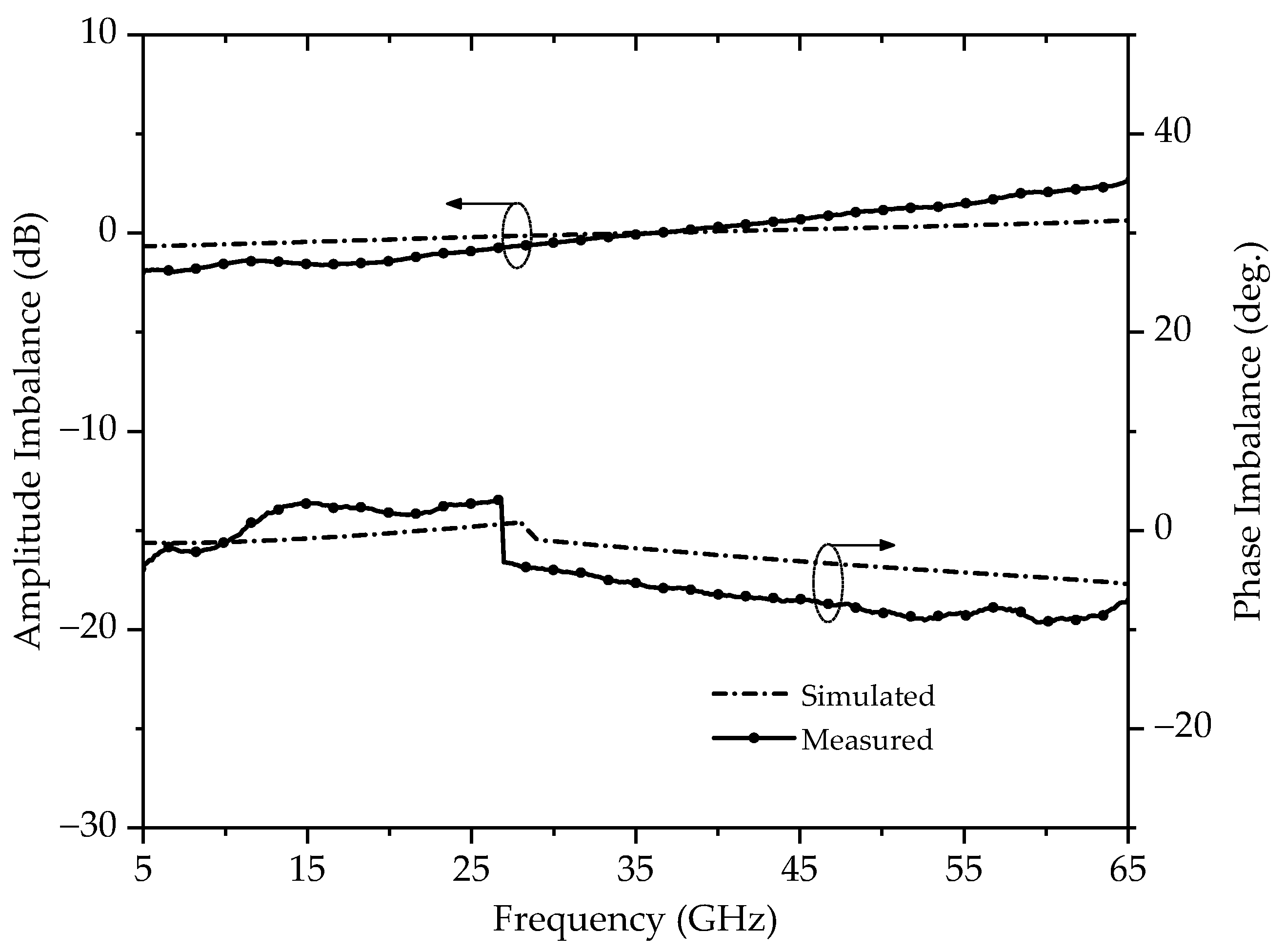
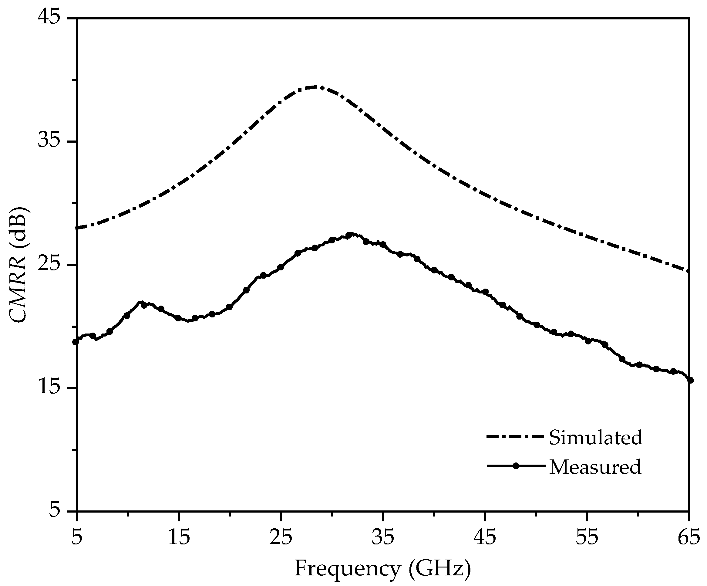
3. Experiment Results
4. Conclusions
Author Contributions
Funding
Conflicts of Interest
References
- Yang, G.; Wang, Z.; Li, Z.; Li, Q.; Liu, F. Balance-Compensated Asymmetric Marchand Baluns on Silicon for MMICs. IEEE Microw. Wirel. Compon. Lett. 2014, 24, 391–393. [Google Scholar]
- Song, I.; Schmid, R.L.; Howard, D.C.; Jung, S.; Cressler, J.D. A 34–110 GHz wideband, asymmetric, broadside-coupled Marchand balun in 180 nm SiGe BiCMOS technology. In Proceedings of the 2014 IEEE MTT-S International Microwave Symposium (IMS2014), Tampa, FL, USA, 1–6 June 2014. [Google Scholar]
- Zhang, J.; Ye, Y.; Sun, X.W. A W-band high conversion gain, single-balanced subharmonically gate-pumped mixer with novel size-reduced Marchand balun. In Proceedings of the 2015 IEEE MTT-S International Microwave Symposium, Phoenix, AZ, USA, 17–22 May 2015. [Google Scholar]
- Xu, L.; Sjoland, H.; Törmänen, M.; Tired, T.; Pan, T.; Bai, X. A Miniaturized Marchand Balun in CMOS With Improved Balance for Millimeter-Wave Applications. IEEE Microw. Wirel. Compon. Lett. 2014, 24, 53–55. [Google Scholar] [CrossRef]
- Tsai, P.; Lin, Y.-H.; Kuo, J.-L.; Tsai, Z.-M.; Wang, H. Broadband Balanced Frequency Doublers With Fundamental Rejection Enhancement Using a Novel Compensated Marchand Balun. IEEE Trans. Microw. Theory Tech. 2013, 61, 1913–1923. [Google Scholar] [CrossRef]
- Chiou, H.K.; Lin, J.Y. Symmetric Offset Stack Balun in Standard 0.13-um CMOS Technology for Three Broadband and Low-Loss Balanced Passive Mixer Designs. IEEE Trans. Microw. Theory Tech. 2011, 59, 1529–1538. [Google Scholar] [CrossRef]
- Xu, Z.; MacEachern, L. Optimum Design of Wideband Compensated and Uncompensated Marchand Baluns With Step Transformers. IEEE Trans. Microw. Theory Tech. 2009, 57, 2064–2071. [Google Scholar]
- Chiou, H.; Yang, T. Low-Loss and Broadband Asymmetric Broadside-Coupled Balun for Mixer Design in 0.18-mm CMOS Technology. IEEE Trans. Microw. Theory Tech. 2008, 56, 835–848. [Google Scholar] [CrossRef]
- Lin, C.S.; Wu, P.-S.; Yeh, M.-C.; Fu, J.-S.; Chang, H.-Y.; Lin, K.-Y.; Wang, H. Analysis of Multiconductor Coupled-Line Marchand Baluns for Miniature MMIC Design. IEEE Trans. Microw. Theory Tech. 2007, 55, 1190–1199. [Google Scholar] [CrossRef]
- Jia, H.; Chi, B.; Kuang, L.; Wang, Z. A W-Band Power Amplifier Utilizing a Miniaturized Marchand Balun Combiner. IEEE Trans. Microw. Theory Tech. 2015, 63, 719–725. [Google Scholar] [CrossRef]
- Chakraborty, S.; Milner, L.E.; Hall, L.T.; Parker, A.; Heimlich, M. A 30–60 GHz SiGe transformer balun with offset radii coils for low amplitude and phase imbalance. In Proceedings of the 2017 IEEE MTT-S International Microwave Symposium (IMS), Honololu, HI, USA, 4–9 June 2017. [Google Scholar]
- Qian, H.J.; Luo, X. Compact 6.5-28.5 GHz On-Chip Balun With Enhanced Inband Balance Responses. IEEE Microw. Wirel. Compon. Lett. 2016, 26, 993–995. [Google Scholar] [CrossRef]
- Mongia, R.; Bhartia, P.; Bahl, I.J. RF and Microwave Coupled-Line Circuits; Artech House: Norwood, MA, USA, 2007. [Google Scholar]
- Leite, B. Design and Modeling of mm-Wave Integrated Transformers in CMOS and BiCMOS Technologies 2012. Ph.D. Thesis, University of Bordeaux 1, Talence, France, 2012; p. 162. [Google Scholar]
- Hsu, H.; Huang, J.-S.; Chen, S.-Y.; Lai, S.-H. Design of an On-Chip Balun With a Minimum Amplitude Imbalance Using a Symmetric Stack Layout. IEEE Trans. Microw. Theory Tech. 2010, 58, 814–819. [Google Scholar]
- Ma, K.; Yan, N.; Yeo, K.S.; Lim, W.M. Miniaturized 40–60 GHz On-Chip Balun With Capacitive Loading Compensation. IEEE Electron Device Lett. 2014, 35, 434–436. [Google Scholar] [CrossRef]


| Topology | Edge Coupled | Broadside Coupled | Proposed |
|---|---|---|---|
| Simulated ILmin (dB) | 1.616 | 1.190 | 0.816 |
| Calculated ILmin (dB) | 1.212 | 1.046 | 0.791 |
| Reference | [11] | [12] | [16] | Proposed |
|---|---|---|---|---|
| Process | 0.13-μm SiGe BiCMOS | 0.13-μm SiGe BiCMOS | 0.18-μm SiGe BiCMOS | 0.13-μm SiGe BiCMOS |
| Topology | Broadside coupled | Broadside coupled | Broadside coupled | Broadside and edge coupled |
| Frequency (GHz) | 30.0–60.0 | 6.5–28.5 | 40.0–60.0 | 29.0–46.0 |
| Insertion loss * (dB) | <3 | <3 | 1.9 | 1.02 |
| Amplitude Imbalance (dB) | <0.14 | <±1.0 | <0.2 | <±0.83 |
| Phase Imbalance (deg.) | <1 | <±1.65 | <2.7 | −3.8 to −7.3 |
| Chip area (μm2) | 200 × 145 | 360 × 150 | 200 × 180 | 270 × 280 |
© 2020 by the authors. Licensee MDPI, Basel, Switzerland. This article is an open access article distributed under the terms and conditions of the Creative Commons Attribution (CC BY) license (http://creativecommons.org/licenses/by/4.0/).
Share and Cite
Yan, J.; Liu, H.; Zhu, X.; Men, K.; Yeo, K.S. Ka-Band Marchand Balun with Edge- and Broadside-Coupled Hybrid Configuration. Electronics 2020, 9, 1116. https://doi.org/10.3390/electronics9071116
Yan J, Liu H, Zhu X, Men K, Yeo KS. Ka-Band Marchand Balun with Edge- and Broadside-Coupled Hybrid Configuration. Electronics. 2020; 9(7):1116. https://doi.org/10.3390/electronics9071116
Chicago/Turabian StyleYan, Jinna, Hang Liu, Xi Zhu, Kai Men, and Kiat Seng Yeo. 2020. "Ka-Band Marchand Balun with Edge- and Broadside-Coupled Hybrid Configuration" Electronics 9, no. 7: 1116. https://doi.org/10.3390/electronics9071116
APA StyleYan, J., Liu, H., Zhu, X., Men, K., & Yeo, K. S. (2020). Ka-Band Marchand Balun with Edge- and Broadside-Coupled Hybrid Configuration. Electronics, 9(7), 1116. https://doi.org/10.3390/electronics9071116