Abstract
A process-voltage-temperature (PVT)-robust, low power, low noise, and high sensitivity, super-regenerative (SR) receiver is proposed in this paper. To enable high sensitivity and robust-PVT operation, a fast locking phase-locked-loop (PLL) with initial random phase error reduction is proposed to continuously adjust the center frequency deviations of the SR oscillator (SRO) without interrupting the input data stream. Additionally, a concurrent quenching waveform (CQW) technique is devised to improve the SRO sensitivity and its noise performance. The proposed SRO architecture is controlled by two separate biasing branches to extend the sensitivity accumulation (SA) phase and reduce its noise during the SR phase, compared to the conventional optimal quenching waveform (OQW). The proposed SR receiver is implemented at 2.46 GHz center frequency in 180 nm SMIC CMOS technology and achieves better sensitivity, power consumption, noise performance, and PVT immunity compared with existent SR receiver architectures.
1. Introduction
The low complexity and low power consumption characteristics make super-regenerative (SR) receivers, mainly composed of a LC-tank super regenerative oscillator (SRO), an envelope detector (ED), and a demodulator, a suitable alternative for short-range wireless communications. Unlike linear receivers which tend to be more robust to PVT variations [1,2], SR receivers are nonlinear and hence are inherently more prone to PVT variations. The in-band SRO gain is simultaneously affected by the frequency deviations between the carrier frequency of the input OOK signal and SRO’s center frequency and the design of its quenching waveform as shown in Figure 1a. Any deviation in the center frequency or the shape of its quenching waveform will result in selectivity and sensitivity degradations. To achieve high performance under low power consumption, a frequency calibration circuit is required to adjust the SRO center frequency and an optimal quenching waveform (OQW) [3] is needed to optimize the SRO performance.
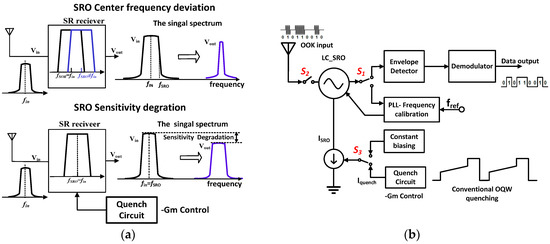
Figure 1.
Challenges in the design of SRR: (a) SRO’s selectivity and sensitivity under PVT (process-voltage-temperature) variations, and (b) the conventional frequency calibration for SR (super-regenerative) receiver with OQW (Concurrent Quenching Waveform).
Recently, several frequency calibration techniques have been proposed for SR receivers using a phase-locked-loop (PLL) [4,5] or a counter-based frequency-locked-loop (FLL) [6] as shown in Figure 1b. Although these techniques can calibrate the SRO to the expected center frequency, they have to interrupt receiving of the input OOK data stream. For example, the frequency calibration loop in Reference [4] uses a charge-pump based PLL to compensate for the frequency deviations of the SRO at start-up; however, it is not able to continuously track the frequency deviation under PVT variations. During normal operation while receiving the input data, any frequency deviation with respects to the SRO nominal center frequency will cause degradation of the SRO performance (as illustrated in Figure 1a). Due to the initial phase error between the reference clock and SRO’s feedback clock at the start of each calibration cycle, the conventional PLL or FLL-based methods need a considerable time exceeding the quenching cycle to overcome this initial phase error and that causes error in the frequency calibration (refer to Section 2.1.1). As a result, it is not feasible to use the conventional techniques to calibrate the SRO frequency in background (refer to Figure 2). In contrast, a novel initial phase error reduction is proposed in this paper to shorten the frequency detection time to less than the quenching cycle. That offers the proposed calibration the capability to continuously adjust the SRO center frequency in every quenching cycle to compensate for the SRO selectivity deviation during normal operation.
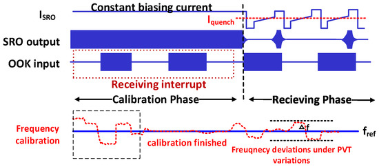
Figure 2.
The timing diagram of the conventional frequency calibration.
The sensitivity of the SR receiver is determined mainly by its quenching signal design. An optimal quenching waveform (OQW), shown in Figure 1b, was proposed in Reference [1] to optimize the sensitivity of the SRO. This quenching signal places the SRO into two regions, namely the sensitivity accumulation (SA) region and the super-regenerative (SR) region. In this paper, a concurrent quenching waveform (CQW) technique is presented to extend the SA region over the entire quenching period to allow maximum sensitivity accumulation and alleviate the requirement on the slope shape of the OQW under PVT variations. In addition, the proposed CQW reduces the SRO noise substantially and improves its signal-to-noise ratio (SNR) during the SR region.
This paper is organized as follows: Section 2 firstly presents the SRO theoretical background analysis and important design parameters, and then introduces the proposed background frequency calibration and concurrent quenching waveform techniques. Section 3 includes the simulation results. Section 4 concludes this paper.
2. Materials and Methods
2.1. SRO Theoretical Background Analysis
2.1.1. PLL with Random Initial Phase Error
To improve the SR receiver selectivity, compensation of its center deviation is required. There are several methods currently used to calibrate the oscillating frequency of the SRO using PLL [4,5] and FLL [6]. However, all of them are infeasible to conduct background frequency calibration as the reason described below.
Figure 3a illustrates the schematic of the SR receiver with a conventional PLL-based frequency calibration. In contrast with the continuous operation of a normal PLL used for clock synchronization, a PLL used for SRO oscillating frequency calibration operates in intermittent mode. when the input enable signal is high, PLL is activated to detect the phase error between the reference clock and the feedback clock , and converts this phase error into the pulse width on the outputs and of the phase-frequency detector (PFD), and accordingly drive the charge pump to adjust the varactors’ tuning voltage to tune the oscillating frequency of SRO to be the desired one. When is low, the PLL must freeze its operation. Since and are unsynchronized when turns active, there exists a random phase error between and as shown in Figure 3b.
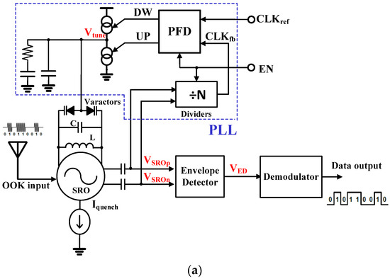
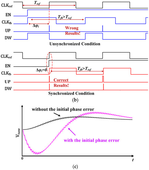
Figure 3.
The challenges of conventional PLL-based frequency calibration: (a) the schematic of the SR receiver with the PLL-based calibration (b) the impacts of the unpredictable initial phase error on the phase error detection and (c) on the settling time of PLL.
The phase difference between and can be expressed as follows:
where and are the frequencies corresponding to and the reference clock and the PLL loop’s feedback clock respectively, is the initial phase error between these two clocks at the start of the detection, and is the detecting time. As shown in Figure 3b, although the period of the reference clock is smaller than the feedback clock’s period , will result in incorrect values at the PFD’s output signals on and , which causes increasing by PLL instead of decreasing it. That will increase substantially the PLL’s settling time (as indicated by the settling time of in Figure 3c), therefore, it is hard for the conventional PLL-based calibration to adapt SRO’s intermittent operation because the quenching cycle is too short for PLL to acquire correct phase error detection. As a consequence, the SR receiver has to interrupt its receiving process and keep SRO oscillating continuously till the finish of frequency calibration.
2.1.2. Quenching Signal Analysis under PVT Variations
To optimize the sensitivity of the SRO, an optimal quenching waveform (OQW) is proposed in Reference [1] as shown in Figure 4. The OQW offers clearly better performance compares with conventional quenching waveforms such as square wave, sawtooth, and sinusoidal quenching. The OQW signal places the SRO into 2 regions, the sensitivity accumulation (SA) region and the super-regenerative (SR) region, to optimize the SRO sensitivity (Figure 5).
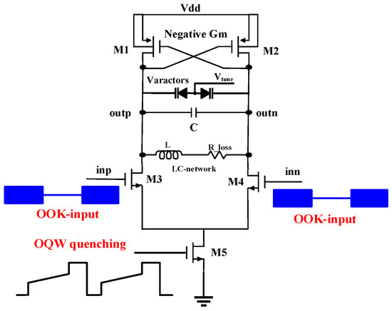
Figure 4.
The conventional SRO architecture with OQW.
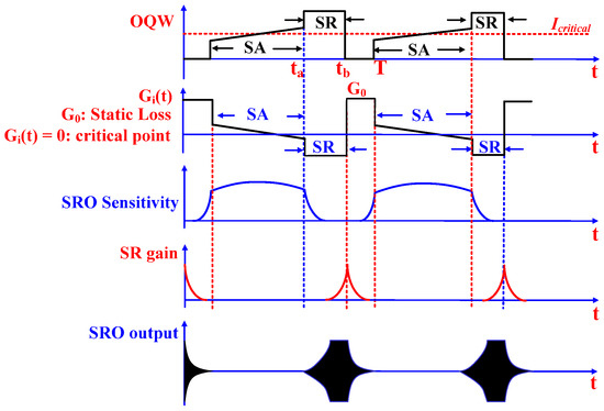
Figure 5.
The timing diagram of the conventional SRO architecture with OQW.
According to Reference [1], the expression of the SRO voltage output can be written as:
where , , represents the passive gain, quiescent damping factor, center frequency of the SRO respectively. is the dynamic damping factor for the entire system and is the first derivative of the input current. The dynamic damping factor is given:
where represents the SRO static loss, is the transient value of the negative transconductance. C is the total capacitance of the LC-tank and represents the instantaneous transconductance due to the quenching controller. The sensitivity and SR gain functions extracted from Equation (2) are:
As it is shown in the timing diagram of the OQW based SRO in Figure 5, the sensitivity reaches its maximum value when the SRO biasing current is equal to a critical current (equivalently when the instantaneous transconductance ). However, once the oscillation starts to build up in the SR region, the SRO will not respond to the input signal because the sensitivity rapidly decays afterwards in the SR region (refer to Figure 5). Since the maximum sensitivity of the SRO is achieved only when the OQW crosses in the middle of SA region, any change in the OQW’s slope due to PVT variations in the SA region will cause sensitivity degradation as shown in Figure 6. At the end of the SA region, the OQW is stepped up to a maximum value to place the SRO in the SR region and regenerate the output signal. In the SR region, the SRO regenerative gain is dramatically reduced because the sensitivity decays to 0 (refer to Figure 6b), therefore, the input referred noise will dramatically increase which will degrade the SNR.
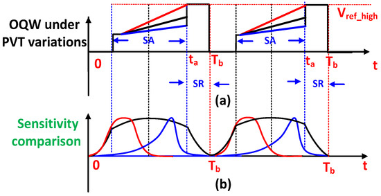
Figure 6.
Optimal quenching waveform under PVT variations: (a) OQW slope variations and (b) sensitivity variations under slope variations.
2.2. Proposed SR Receiver with Background Frequency Calibration and Concurrent Quenching Waveform
2.2.1. SR Receiver Architecture Overview
The block diagram of the proposed SR receiver is illustrated in Figure 7. This receiver consists of an SRO quenched by the proposed CQW and a PLL with the initial phase error reduction, built around the SRO for frequency calibration. Beside the components illustrated in Figure 3a, the proposed PLL includes an initial phase error reducing circuit (IPERC), a comparator (COM) used to trigger frequency calibration periodically, a divider (CT1) employed to generate a synchronized reference clock from the input clock , and an analog OTA-based buffer to drive the varactors and hold the charge on the capacitor . Unlike the above mentioned PLL or FLL techniques in References [4,6] that interrupt the receiving phase to perform frequency calibration, the proposed PLL can perform frequency calibration without disturbing the data receiving. When the envelope detector output goes high, exceeding a preset threshold voltage , the output of comparator COM in PLL turns high accordingly to enable PLL to detect the frequency difference between the SRO output frequency and the desired one, and tune the SRO center frequency via the voltage . Meanwhile, the proposed CQW technique is applied to the SRO to achieve noise reduction and sensitivity enhancement robust to PVT variations.
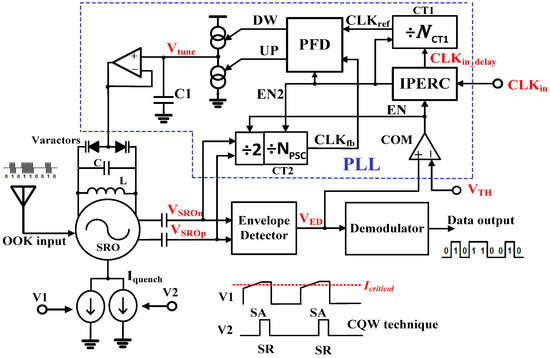
Figure 7.
The block diagram of the proposed SR receiver with background frequency calibration and CQW technique.
2.2.2. Fast Frequency Calibration Using PLL with Initial Phase Reduction
As shown in Figure 7, the proposed PLL is composed mainly of a phase detector, a high-speed analog divider (÷2) combined with a pulse-swallow counter (CT2) for RF signal frequency division, a counter (CT1) for the reference clock generation, an initial phase error reduction circuit (IPERC), and a comparator (COM). IPERC is used to eliminate the initial phase error between the reference clock () and the feedback clock () stemming from SRO’s output. After initial phase error reduction, the actual phase error between and is detected by the phase detector and converted into the pulse width on the phase detector’s output and . Then, and drive the charge pump to charge or discharge the capacitor to adjust its voltage . Finally, the voltage on is buffered and fed to the varactors to tune SRO’s oscillating frequency.
The required frequency calibration time per quenching cycle for the proposed intermittent frequency calibration technique is much shorter than conventional techniques mentioned in Reference [1,2,4] owing to the initial phase error reduction. Equation (6) shows the design parameters which will influence the calibration time. The phase detector output represents the frequency detecting accuracy and can be derived as:
where is the initial phase error occurring in the nth cycle, represents the phase detecting time, is the overall division ratio including the ratio of the analog divider (÷2) and from CT2 respectively; and are the frequency of and respectively, and is the result of dividing by the division ratio of CT1. is defined as the calibration resolution which represents the difference between the desired SRO oscillating frequency and the current SRO oscillating frequency. As indicated, the ultimate phase error includes the unpredictable and the actual phase error between and .
Compared with the conventional counterparts in the sate-of-art design, IPERC is the essential of the proposed PLL. Figure 8 shows the schematic of the IPER and its signal propagation delay diagram, while Figure 9a illustrates its timing diagram.
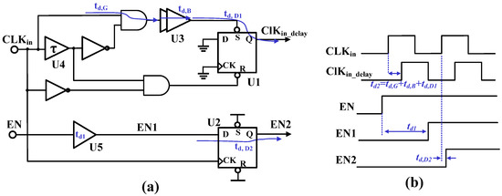
Figure 8.
The initial phase error reduction principle: (a) the schematic and (b) its signal propagation delay.
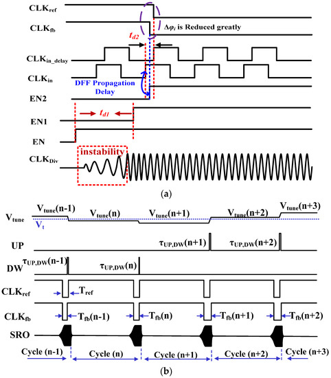
Figure 9.
The timing diagram of the proposed PLL calibration with IPRC: (a) the timing diagram of the initial phase error reduction, and (b) the critical signals in the proposed PLL (assuming quasi-periodic steady state).
In conjunction with those figures, the working principle of IPERC is explained as follows. This circuit includes two identical DFF-type latches, U1 and U2, with a set (S) and a reset (R) inputs. The latch U1 along with a buffer chain (U3), a delay cell (U4), two AND2 gats and two inverters are used to generate which is a delayed version of the input . The input is delayed by through the delay cell U5 to generate the signal which is sampled in U2 by to generate the output . As shown in Figure 8b, the rising edges of will lag behind the corresponding rising edges of by a delay of calculated by:
where is the AND gate’s propagation delay, is the buffer chain’s delay, and is the latch’s propagation delay from its input S to its output Q.
Simultaneously, the rising edge of will lag behind the rising edges of by a delay of , the latch U2’s propagation delay from its clock input CK to its output Q. The delay of on is aimed at preventing the division ratio from the instability of the analog divider during the initial start-up phase as shown in Figure 9a. To avoid the degradation of detecting accuracy caused by the instability, the value of must be set greater than the settling time of the analog divider. The duration of the instability varies with PVT variation, and its worst-case scenario is about 5 ns in the proposed design, hence is set to 10 ns in this design.
As shown in Figure 7, is used to enable the dividers CT1 and CT2 at the same time to synchronize the generation of and , and consequently eliminate their initial phase error . According to Equation (7), the rising edge of will always lead the rising edge of by a value of . That prevents CT1 from missing the first rising edge of when turns high. Since approximately equals , can be set by the buffer chain U3 to provide synchronization between with . As a result, can be reduced from tens nanoseconds to less than 1 ns despite PVT variations.
Figure 9b presents the timing diagram of the main signals in the proposed PLL. The PLL operates on cycle by cycle basis by detecting the frequency error between and , and adjusting the tuning voltage and consequently the oscillating frequency of SRO in each cycle. To systematically analyze its performance, the following hypotheses are considered: (1) the PLL operated in a quasi-periodic steady state mode; (2) The transient charging or discharging behavior of the charge pump is neglected. After calibration, the negative pulse width of approximately equals , the counterpart of ; while the tuning voltage will approach the desired level . Therefore, the following equations can be found:
where is the initial phase error in the cycle , is the pulse width of PFD’s outputs; is the current of the charge pump; is the capacitance of C1; and is the voltage-to-frequency gain of SRO (assumed to have a negative value), is the oscillating frequency of SRO while is its initial value. Those equations can be combined as:
It is notable that equals the target frequency which is expected to be . Additionally, ∆Vtune(n)∆Tfb(n) is sufficiently small compared to other terms in Equation (9), and can be neglected. The Equation (9) can be rewritten as:
Substituting Equation (10) into Equation (8) yields:
By applying Z-domain analysis to Equation (11), the transfer function of the PLL can be written as:
As implied by Equation (12), the necessary and sufficient condition for the stability of the proposed PLL is:
The step response of the system can be written as:
From the above equation, it can be observed that a larger can lead to a faster system’s convergence but results in a larger ripple on . In this design, is set to 0.27 to guarantee accurate frequency calibration as it is discussed in Section 3.
2.2.3. SRO with Concurrent Quenching Waveform
The proposed SRO architecture and its timing diagram are shown in Figure 10 and Figure 11 respectively. In contrast to conventional SRO architectures, the SA and SR regions in the proposed one are separately controlled by M5 and M6 which perform the proposed CQW operation. M5 is controlled by and is on for the entire quenching period (case when in Figure 11). M6 is controlled by and is on only during the SR region. When M5 is on, the SRO is always operating in the vicinity of Icritical and accumulates sensitivity during the entire quenching phase. When M6 is on, the SRO performs super-regeneration and sensitivity accumulation simultaneously, while the conventional SRO architecture with OQW loses sensitivity accumulation during SR region. When the transistors M5–6 are both on, the SRO is in SR region and concurrently regenerates the SRO output and samples the input signal for the entire quenching cycle.
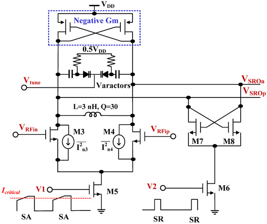
Figure 10.
The proposed SRO architecture with CQW technique.
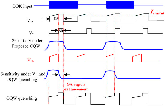
Figure 11.
Comparison between the conventional OQW and the proposed CQW techniques.
Splitting the quenching signal into and allows optimizing the noise performance in addition to improving the accumulated sensitivity compared to OQW as will be explained later. Figure 12c shows the SRO output noise with different waveforms, and , along with OQW scheme. For , M5 is on for the entire quenching period to improve sensitivity and noise compared to OQW. For M5 is turned off to improve more the noise performance compared to the case of while achieving same sensitivity as OQW.
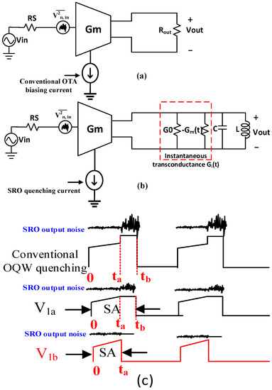
Figure 12.
Noise analysis comparison between conventional OTA and SRO: (a) small signal model for OTA, and (b) SRO; (c) SRO quenching strategy and noise performance comparison.
To understand how to optimize the noise of the SRO it is instructive to compare the noise performance of an OTA and an SRO as shown in Figure 12a,b. The small signal model of an OTA and SRO are different by the type of load. Additionally, the OTA is biasing using constant current while an SRO is biased using its customized quenching waveform. The output referred noise of an OTA can be analyzed as follows:
where and are the input and output referred noise respectively. Gain of an OTA, simply equals . Since the biasing current is a constant value which means that the maintains a constant value. In conventional linear receivers with OTA placed as the front-end signal detector, increasing the biasing current will cause input referred noise to decrease because the current thermal noise of an MOS transistor is proportional to while the input referred noise is inversely proportional to .
Similarly, the input referred noise of the SRO can be intuitively analyzed also by starting from the SRO gain [7,8] as the following:
with
where is the SRO regenerative gain and is the SR gain as given in Equation (5).
The gain can also be written as the following:
where is the the equivalent noise bandwidth (ENB) of the SRO frequency response. and refer to the effective transconductance of M3–4 in Figure 10 and static loss of the SRO. For practical design purposes, in Equations (16)–(19) the SRO regenerative gain is much greater than the SR gain for the SRO to achieve good sensitivity. The noise bandwidth in Equation (18) is determined by the selectivity of the SRO.
As we can notice, the major difference for the noise analysis between conventional OTA-based receivers and SR receiver is that the gain of an SRO is consists of 3 different components, namely static loss, regenerative gain, and super-regenerative gain corresponding to respectively. For the proposed CQW scheme applied as quenching signal for the SRO under , the sensitivity region has been extended over the entire quenching cycle and the SRO is always responding to the input OOK signal for both SA and SR regions. Therefore, the major contribution of the SRO gain is not degrading through the entire quenching cycle and hence reducing the input referred noise and improving the SNR. In contrast, for the SRO under OQW quenching, the SR region is only responsible for generating the oscillation envelope, in response to the SA region, while is dramatically reduced because the sensitivity decays to 0 (refer to Figure 11). Therefore, the input referred noise will dramatically increase and hence degrade the SNR. It is straightforward to find that the SRO frequency response has narrower noise bandwidth for the proposed CQW technique compared with the conventional OQW quenching because the proposed CQW technique extends the sensitivity for the SRO in time domain and therefore, it automatically reduces the to reduce the noise.
The dominant noise source of the SRO circuits is stemmed from the input transistors (M3–4 in Figure 10); when the transistors M3-M4 are turned off in SO region to reduce the noise as highlighted in red in Figure 12c. That will maintain the same SA region compared with the OQW while reducing the biasing current completely in the SR region for the input transistors M3–4 to maximize the SNR for the SRO under the trade-off of lower sensitivity accumulation compared to the case of .
3. Simulation Results and Discussion
The proposed SR receiver with PLL frequency calibration and CQW technique is implemented in at transistor level using 180 nm SMIC CMOS technology. An inductor of 3 nH with a quality factor (Q) of 30 and a pair of varactors with a nominal capacitance of 0.5 pF (at ) are used to set the SRO resonance frequency around 2.46 GHz. A Gm-boosted crossing-coupled PMOS pair with an aspect ratio of 450/0.18 is used to provide sufficient negative transconductance under a supply voltage of 1 V. The aspect ratio of input pair (M3/M4/M7/M8) in Figure 10 is 150/0.18.
Figure 13 is the simulation results to illustrate the operating principle of the proposed SRO with CQW technique. The CQW extends the SA region during the control voltage , while is only used to generate fast start-up oscillation. As a result, the effect of the process variation on slope changes can be reduced. As shown, the process variations does not degrade the sensitivity accumulation because the SA region has been extended over the entire quenching cycle and the SRO is able to detect the input signal correctly with different slopes of the voltage .
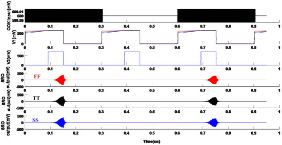
Figure 13.
The simulation results illustrating the SRR’s immunity against process variations when the proposed quenching waveform is applied. From top to bottom: the input OOK signal, the proposed CQW voltage under process variations, the proposed CQW voltage , and the SRO output signals under process variations (the red line for the fastest-speed process corner (FF), the black is for the typical (TT), and the blue is for the slowest one (SS)).
In contrast to Figure 13, Figure 14 show how the conventional OQW suffers under process variations which dramatically reduce the sensitivity of the SRO. That is indicated from the oscillation at the SRO output during the absence of input OOK signal. Figure 15 and Figure 16 show the immunity of the proposed the proposed CQW architecture against voltage and temperature variations respectively. Figure 17 shows how the proposed CQW architecture can reduce the oscillation at the SRO output during the absence of input signal with the presence of noise compared with OQW. That is indicated by reducing the oscillation at the SRO output during the absence of input OOK signal.
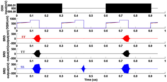
Figure 14.
The simulation results illustrating the SRR’s immunity against process variations when the conventional optimal quenching waveform is applied. From top to bottom: input OOK signal, the combined CQW waveform, and the SRO output signals under process variation (the red line for the fastest-speed process corner (FF), the black is for the typical (TT), and the blue is for the slowest one (SS)).
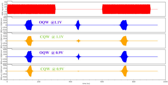
Figure 15.
The simulation results illustrating the SRR’s immunity against supply voltage variations. From top to bottom: the input OOK signal, the OQW @ 1.1V, the proposed CQW @ 1.1V, the OQW @ 0.9V, and the proposed CQW @ 0.9V.
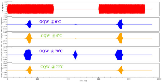
Figure 16.
The simulation results illustrating the SRR’s immunity against temperature variations. From top to bottom: the input OOK signal, the OQW @ 0 °C, the proposed CQW @ 0 °C, the OQW @ 70 °C, and the proposed CQW @ 70 °C.
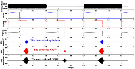
Figure 17.
The simulation results illustrating noise analysis comparison between the proposed CQW technique and the conventional OQW technique. From top to bottom: the input OOK signal, the proposed CQW quenching voltage , the proposed CQP quenching voltage , the conventional OQW quenching voltage, and the SRO output signals corresponding with different quenching waves.
Figure 18 shows the proposed PLL with initial phase error reduction. is set to 50 MHz and the division ratio of and are 5 and 123 respectively to expect a final of 2.46 GHz. As Figure 16 indicates, due to the random initial phase between and , the time shift can be up to 18 ns. However, by applying the proposed initial phase error reduction, the actual phase error can be shortened to be around 0.12 ns. Therefore, the proposed PLL can differentiate the small frequency deviation between and and then adjust the voltage in each calibration cycle. Figure 19 illustrates the proposed frequency calibration process during SR receiver’s receiving. In simulations, each quenching cycle lasts 1.25 μS to match a data rate of 800 kbps wherein the SR phase only occupies a length of 300 ns. Despite the short SR phase, the proposed PLL is still able to adjust the oscillating frequency from 2.55 GHz to 2.46 GHz with a frequency error of less than 10 MHz as shown. In contrast, when the initial phase error reduction is disabled, the PLL fails to obtain sufficiently precise frequency error detection, and the initial phase error misleads the adjustment of . As a result, the PLL finally settles down to a wrong as shown in Figure 20.
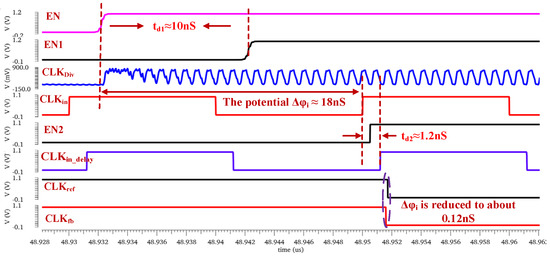
Figure 18.
The simulation results of the proposed phase error reduction under clock synchronization and delay compensation.
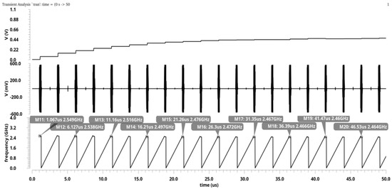
Figure 19.
The simulation results of the proposed background frequency calibration, sequentially including: the control voltage, SRO’s output signal, and the frequency calibration results (the calibration results in each quenching cycle have been labeled).
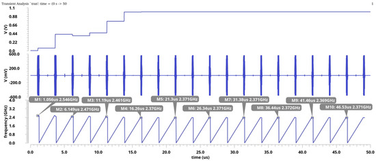
Figure 20.
The simulation results without the proposed initial phase error reduction, sequentially including: the control voltage, SRO’s output signal, and the frequency calibration results (the calibration results in each quenching cycle have been labeled).
In the following simulation the immunity of the proposed PLL is evaluated under technology process variations. The SRO’s frequency versus voltage curves are tested with corners variation as shown in Figure 21. The frequency variation can be up to 50 MHz with a fixed due to the process variation while the voltage-to-frequency gain is about −267 MHz/V at under the TT process corner. Figure 22a shows the settling behavior of PLL is with different values of changed by selecting different according to Equation (13). As shown in Figure 22a, when is less than 2, all waveforms of gradually converge but with ripple due to the random in each cycle. A larger leads to a faster convergence, but more ripples. To achieve a precise frequency calibration, is set to 0.27. In this case, the settling time of PLL is about 35 μs, and the ripple of is limited to less than 25 mV which corresponds to a frequency variation of 6.7 MHz. Figure 22b shows the settling behavior under various process corners with . It can be seen that the waveforms can converge regardless of the process variation with a maximum voltage ripple less than 25 mV.
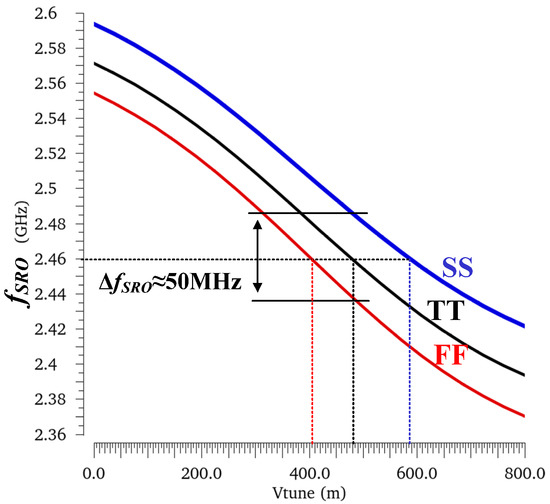
Figure 21.
The simulation curves of vs under different process corners.
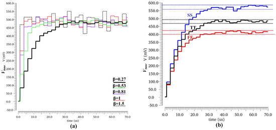
Figure 22.
The simulated settling waveforms of (a) with different values of , and (b) under process variation with a constant .
Figure 23 shows the breakdown power consumption of the proposed SR receiver. The total power consumption of the receiver is about 802 μW, including the main blocks of the receiver: the SRO, the envelop detector (ED), and the demodulator (Dem.), contributes a power consumption of about 395 μW; while the PLL consumes a power of 407 μW in average. Table 1 summarizes the performance of this work in comparison with the state-of-arts. The main features of the proposed design are the ability to achieve background frequency calibration with a good sensitivity and less power consumption compared to the counterparts.
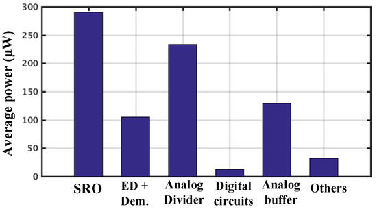
Figure 23.
The simulated power consumption summary.

Table 1.
Performance table and comparison to the prior works.
4. Conclusions
This paper proposed a new background frequency calibration and quenching techniques to improve the sensitivity and selectivity of SR receiver. In this work, the importance of cancelling of the initial phase error is discussed and frequency calibration using a PLL with the initial phase error reduction has been proposed to calibrate the SRO center frequency without interrupting the incoming data stream and simultaneously improving the selectivity of the SR receiver. The proposed architecture achieves much shorter phase detecting time to support discrete frequency calibration compared with conventional techniques. Moreover, the proposed CQW quenching technique allows the sensitivity accumulation region to be enlarged through the entire quenching cycle which improves the SRO sensitivity, noise performance, and reduce the power consumption compared with conventional SRO architecture. Meanwhile, immunity to PVT variations has also been improved due to the SA region extension.
Author Contributions
All the authors contributed substantially to this paper. The conceptualization, methodology, validation, and formal analysis of PLL, Y.Y.; The conceptualization, methodology, validation, and formal analysis of CQW, X.F. and K.E.-S.; investigation, Y.Y.; writing—original draft preparation, Y.Y., and X.F.; writing—review and editing, Y.Y. and K.E.-S.; funding acquisition, Y.Y., and K.E.-S.
Funding
This research was partly funded by THE FUJIAN PROVINCIAL NATURAL SCIENCE FOUNDATION OF CHINA, grant number 2017J01760, and 2017J01734, and THE NATURAL SCIENCE AND ENGINEERING RESEARCH COUNCIL OF CANADA.
Conflicts of Interest
The authors declare no conflicts of interest.
References
- Kopta, V.; Barras, D.; Enz, C.C. An approximate zero IF FM-UWB receiver for high density wireless sensor networks. IEEE Trans. Microw. Theory Tech. 2017, 65, 374–385. [Google Scholar] [CrossRef]
- Selvakumar, A.; Zargham, M.; Liscidini, A. Sub-mW current reuse receiver front-end for wireless sensor network applications. IEEE J. Solid-State Circuits 2015, 50, 2965–2974. [Google Scholar] [CrossRef]
- Fernandez-Rodriguez, F.; Sanchez-Sinencio, E. Advanced Quenching Techniques for Super-Regenerative Radio Receivers. IEEE Trans. Circuits Syst. I Regul. Pap. 2012, 59, 1533–1545. [Google Scholar] [CrossRef]
- Chen, J.; Flynn, M.; Hayes, J. A fully integrated auto-calibrated super-regenerative receiver in 0.13-μm CMOS. IEEE J. Solid-State Circuits 2007, 42, 1976–1985. [Google Scholar] [CrossRef]
- Tung, C.-J.; Liu, Y.H.; Liu, H.H.; Lin, T.H. A 400-MHz super-regenerative receiver with digital calibration for capsule endoscope systems in 0.18-μm CMOS. In Proceedings of the 2008 IEEE International Symposium on VLSI Design, Automation and Test (VLSI-DAT), Hsinchu, Taiwan, 23–25 April 2008; pp. 43–46. [Google Scholar]
- Rezaei, V.D.; Entesari, K. A Fully On-Chip 80-pJ/b OOK Super-Regenerative Receiver with Sensitivity-Data Rate Tradeoff Capability. IEEE J. Solid-State Circuits 2018, 53, 1443–1456. [Google Scholar] [CrossRef]
- Favre, P.; Joehl, N.; Vouilloz, A.; Deval, P.; Dehollain, C.; Declercq, M. A 2-V 600-μA 1-GHz BiCMOS super-regenerative receiver for ISM applications. IEEE J. Solid-State Circuits 1998, 33, 2186–2196. [Google Scholar] [CrossRef]
- Moncunill-Geniz, F.X.; Pala-Schonwalder, P.; Mas-Casals, O. A generic approach to the theory of super-regenerative reception. IEEE Trans. Circuits Syst. I Regul. Pap. 2005, 52, 54–70. [Google Scholar] [CrossRef]
© 2019 by the authors. Licensee MDPI, Basel, Switzerland. This article is an open access article distributed under the terms and conditions of the Creative Commons Attribution (CC BY) license (http://creativecommons.org/licenses/by/4.0/).