


Abstract
This paper presents an in-depth analysis of a non-isolated buck–boost DC–DC converter which uses coupled inductors. The converter is designed to achieve a high static conversion ratio while using a moderate number of semiconductor devices. The proposed topology, originally introduced in a former paper of the authors, under ideal operating conditions, is now evaluated taking into account non-ideal components, modeling the conduction losses of the semiconductor devices and the equivalent series resistance of the output capacitor. In order to get a regulated output voltage, closed-loop behavior is also investigated. By using the state-space modeling approach, the calculation of the converter static conversion ratio and control-to-output transfer functions is performed. Because the topology is of fourth order, a procedure for controller design is provided. A type III error amplifier is chosen, and the pole-zero placement technique is used for its design, demonstrating that the classical control strategy still works even with this fourth-order converter. Thus, a good phase margin of 62.3 degrees is achieved. The theoretical results are validated both on open-loop and closed-loop operation, in the presence of conduction losses. Furthermore, a laboratory prototype is implemented, and it validates the theoretical and simulation results. The study demonstrates that the proposed coupled inductors buck–boost converter is a good choice for step-up applications that need a large difference between input and output voltages.
1. Introduction
The rapid growth of renewable energy systems, electric vehicles (EVs), portable electronics, and DC microgrids has increased the demand for flexible and efficient power conversion interfaces. DC–DC converters are very important for setting the voltage levels, ensuring power quality, and managing energy in a wide range of circumstances and operating conditions.
Buck–boost converters [1] are a widely used class of DC–DC converters because they are capable of increasing or decreasing the input voltage depending on what the application requires. Examples include photovoltaic systems (PV) that modify under changing irradiation, battery-powered systems that charge and discharge, fuel-cell energy conversion, and electric vehicle powertrains. In these cases, the converter needs to keep the output voltage stable even when the input voltage and load conditions change a lot. It also needs the converter to be small, efficient, and not put too much stress on the components.
The conventional buck–boost topology has an output voltage that is opposite to the input voltage [2]. Many topologies [3] based on the classical buck–boost architecture have been suggested in the literature. These include switched-capacitor cells [4], switched-inductor [5,6,7,8,9], coupled inductors [10], semi-quadratic or quadratic type [11,12,13], hybrid structures [14], interleaved, transformer-based cells [15], or soft-switching buck–boost topologies.
For renewable-energy and DC microgrid applications, a single-switch, non-isolated buck–boost DC–DC converter derived from the Ćuk topology, capable of achieving a wide voltage conversion ratio with continuous input and output currents and negative output polarity, is shown in [16]. Having three inductors, four capacitors, two diodes, and one transistor, the proposed converter attains a quadratic voltage gain at moderate duty cycles while significantly reducing current stress on the active switch and improving overall efficiency. Other structures with inverted output polarity are presented in [17]. There, three fourth-order buck–boost converter topologies with continuous input and output currents providing minimum-phase behavior through reverse inductor coupling are shown.
For medium-voltage renewable-energy applications such as offshore wind farms, a modular, non-isolated hybrid interleaved DC–DC converter based on an input-parallel output-series (IPOS) structure that integrates an inverting and a non-inverting buck–boost converter to achieve high voltage gain with reduced component count is described in [18]. Interleaved PWM operation enables a significant reduction in input current ripple and output voltage ripple, while the IPOS configuration halves the voltage and current stress on power devices and passive components.
A comprehensive review of non-isolated DC–DC converter topologies frequently used in renewable energy systems, with a specific focus on photovoltaic applications, can be read from [19]. Another review regarding the state-of-the-art of unidirectional, non-isolated single-phase power factor correction (PFC) converters, presented in [20], classifies the converters into fundamental and modified topologies and evaluates them in terms of power factor, total harmonic distortion, efficiency, power rating, and voltage range for both low-voltage and high-voltage EV battery applications. Both reviews provide practical performance comparisons and design-oriented insights, offering clear guidelines for selecting suitable PFC converter topologies for short- and long-distance EV charging systems. In [21] a comprehensive review and comparative analysis of DC–DC buck–boost and boost converter topologies for integrating fuel cells (FCs) into electric vehicles and DC microgrid applications is presented. The study highlights that single-switch buck–boost converters and boost converters employing impedance networks, particularly switched-inductor configurations, offer a favorable trade-off between high voltage gain, efficiency, and suitability for FC systems, providing practical guidelines for topology selection in EV and microgrid applications.
A family of extended boosting range non-isolated buck–boost converter (NIBBC) topologies that provide continuous input current, a common grounded structure, and enhanced quadratic voltage conversion ratio, can be found in [22].
Another family of non-isolated inverting buck–boost DC–DC converters with extended step-down and step-up voltage conversion ratios, including the inverting buck2–boost converter (IB2BC) and the inverting buck–boost2 converter (IBB2C), is shown in [23]. Without using transformers or coupled inductors, the proposed fourth-order converters achieve high voltage gain at moderate duty cycles, common-ground structures, low component voltage and current stress, and avoidance of capacitor voltage discontinuities.
A novel isolated buck–boost DC–DC converter capable of operating in buck, buck–boost, and boost modes while providing a wide input voltage regulation range and galvanic isolation is presented in [24]. The topology employs a current-fed structure with a three-winding high-frequency transformer and six active switches, enabling zero-voltage switching (ZVS) for all main devices across all operating modes. It demonstrates that the converter is able to provide a constant output voltage over a wide input range and is suitable for photovoltaic microconverter applications [24].
A single-switch, non-isolated buck–boost DC–DC converter featuring a quadratic voltage gain and a wide voltage conversion range is shown in [25]. The proposed topology operates in both step-up and step-down modes, shares a common ground between input and output, and requires only one active switch, resulting in simple control and gate-drive implementation. This converter can be used in renewable energy applications where solar or wind variation uncertainties are typically present. The proposed topology from [26] is a non-isolated, unidirectional buck–boost DC–DC converter employing an active switched-inductor (ASI) configuration to achieve high voltage gain with a reduced number of components. This converter ensures continuous input current, noninverting output voltage, and reduced voltage and current stress on switches and passive components. A modified buck–boost converter with a boost stage included, yielding a quadratic voltage gain in boost mode and strong step-down capability in buck mode with a low number of components, is proposed in [27]. This non-isolated buck–boost DC–DC converter achieves a wide voltage conversion range, while significantly reducing the voltage stresses on semiconductor devices and maintaining continuous input current.
In [28], the analysis and implementation of a two-stage isolated twin buck–boost DC–DC converter for electric vehicle (EV) battery charging applications is described. The architecture combines a CLLC resonant isolation stage with a twin buck–boost converter, enabling wide output voltage regulation suitable for both normal and fast charging modes while reducing voltage stress on power devices. A comparative evaluation of proportional–integral (PI) and fuzzy logic controllers (FLC) demonstrates that the FLC achieves superior dynamic performance in terms of reduced rise time, settling time, and steady-state error.
A paper review on error-reduction techniques for closed-loop buck–boost converters by comparatively analyzing classical PID, fuzzy logic control (FLC), hybrid fuzzy–PID, and model predictive control (MPC) strategies is presented in [29].
One of the main goals of all these works is to get a higher voltage gain, less voltage ripple, better efficiency, or more power density. The primary benefit of buck–boost converters that use coupled inductors is that they can get a much higher voltage conversion ratio, provided that the right duty cycle and turns ratio are chosen. Changing the turns ratio can greatly improve the converter’s ability to step up or step down while keeping the voltage stress on the semiconductor devices at a moderate level. These features make these types of converters especially suitable for applications that require high conversion ratios [30], like renewable energy systems [31,32,33], electric vehicles [34], and battery management systems [35,36,37]. Another benefit is that the usage of coupled inductors allows for improved energy transfer and causes less stress on the power switches than in the classical buck–boost converter.
In the paper [38], a wide step-up and step-down Ćuk-type converter is presented, with inverted output polarity. This converter employs coupled inductors, a reduced number of passive components, and a higher voltage gain at the same duty cycle compared to the classical Ćuk. A coupled-inductor buck–boost DC–DC converter (CIBuBoC) that achieves an ultra-wide step-up/step-down voltage conversion ratio with continuous input current, common ground, and positive output polarity is shown in [39]. By employing two simultaneously operated switches and a coupled inductor with an adjustable turns ratio, the converter provides semi-quadratic voltage gain, reduced device voltage stress, and a tunable step-up/step-down boundary. Comprehensive steady-state analysis, loss modeling, and state-space averaged small-signal modeling are presented, and the experimental results demonstrate high efficiency, low input current ripple, and superior performance compared with existing high-gain buck–boost converters for photovoltaic applications. A coupled inductor soft-switching non-isolated DC/DC converter family with double synchronous rectification can be found in [40]. By relocating the auxiliary coupled inductor branch and replacing the auxiliary diode with a synchronously controlled MOSFET, zero-voltage switching is achieved for all active switches without increasing control complexity [40]. In [41], a non-isolated, coupled-inductor-based bidirectional buck–boost DC–DC converter with high voltage gain and soft-switching capability for DC microgrid applications is described. The proposed converter’s main switches work in ZVS mode, while its auxiliary switches work in ZCS mode.
The buck–boost converter proposed in the present paper falls in the same category of coupled-inductor topologies. It was first introduced in [42], and that work focused primarily on the ideal operating conditions, providing the theoretical dc analysis, along with simulation results. That paper also includes some aspects regarding the non-ideal converter, with conduction losses considered, as well as a comparative representation of the ideal and non-ideal theoretical and simulated static conversion ratio. This makes the converter work more effectively in general, especially in step-up conditions.
The purpose of the present paper is a continuation of [42], which stopped at the simulation level, by further investigating the proposed converter and addressing a number of complementary aspects. First, a comparison of the circuit static conversion ratio with those of other step-up/step-down topologies highlights its most important features. Second, a more in-depth examination of the non-ideal converter is performed utilizing a state-space modeling approach. This allows a small-signal analysis to be performed, thus finding the control-to-output transfer function of the proposed topology and the controller to be designed. Finally, the converter is practically implemented, and the results are presented.
The comparative analysis of the converter, together with state-space matrices and how the control-to-output transfer function was obtained, is presented in Section 2. Also, the design of the type III error amplifier can be found in the same section. Section 3 presents the simulation results of the proposed converter with conduction losses considered, both in open-loop and closed-loop situations. In the same section, the practical implementation of the converter, followed by a comparison between theoretical and experimental results, is also available. The research results are discussed in Section 4, and the paper ends with the conclusions drawn in Section 5.
2. Materials and Methods
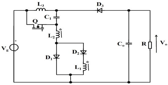
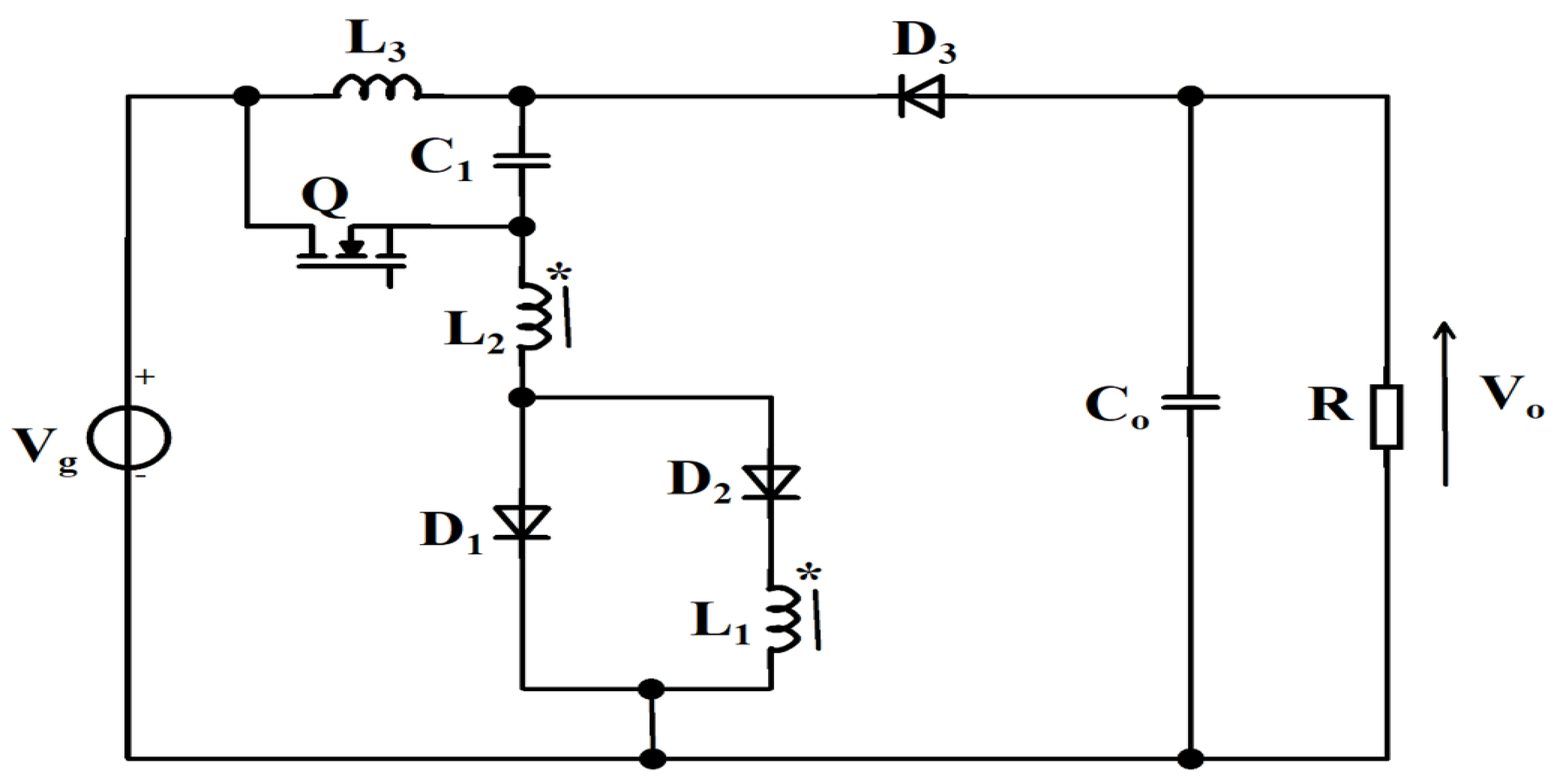
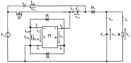
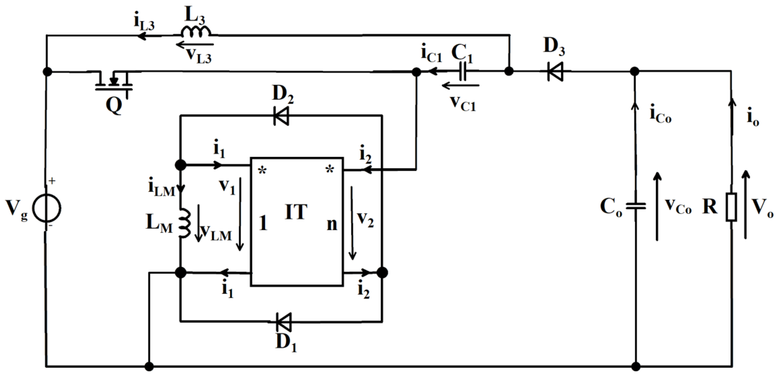
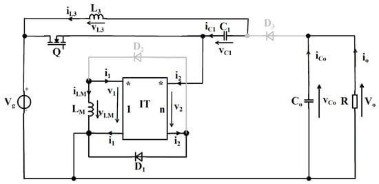
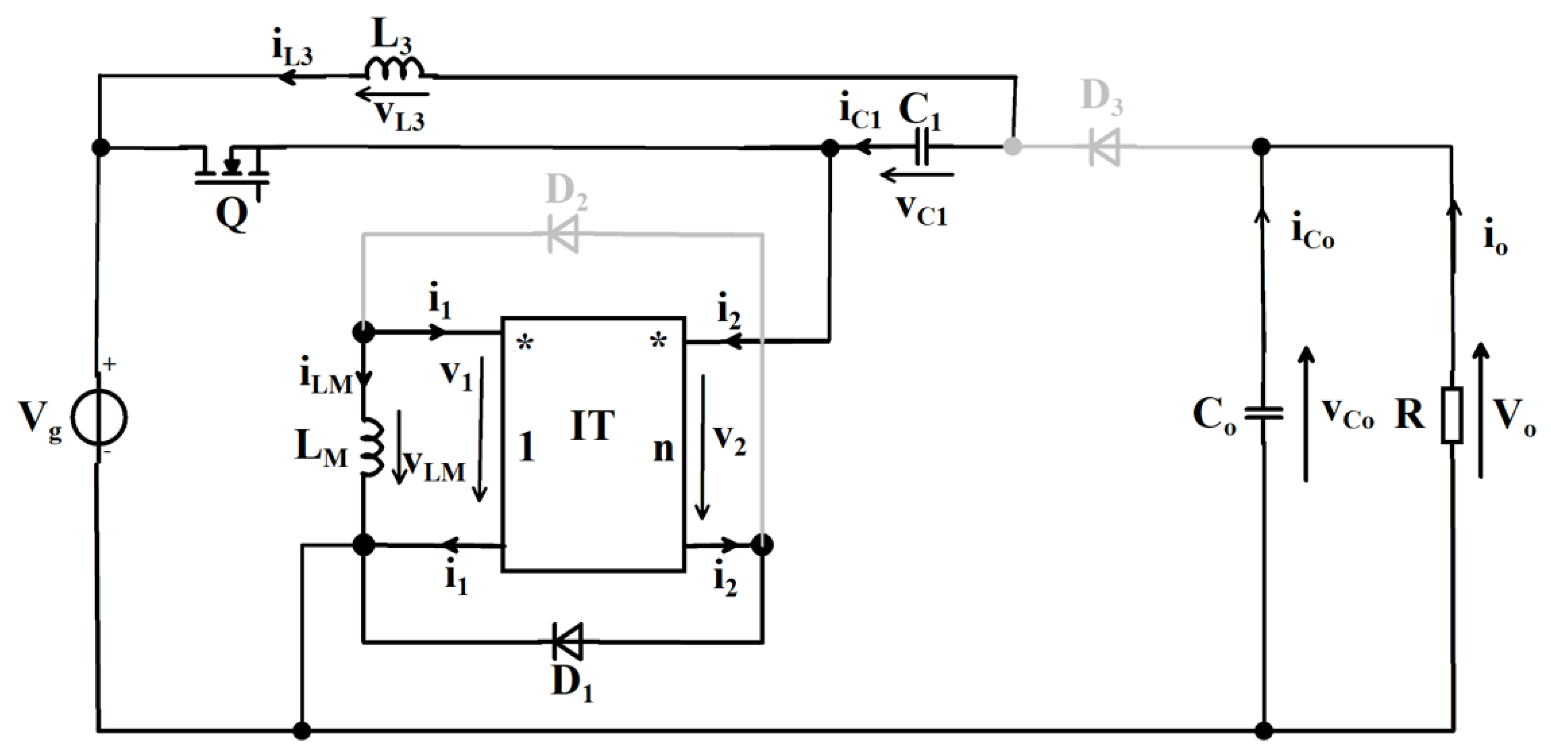
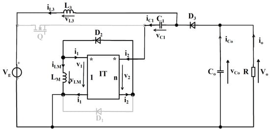
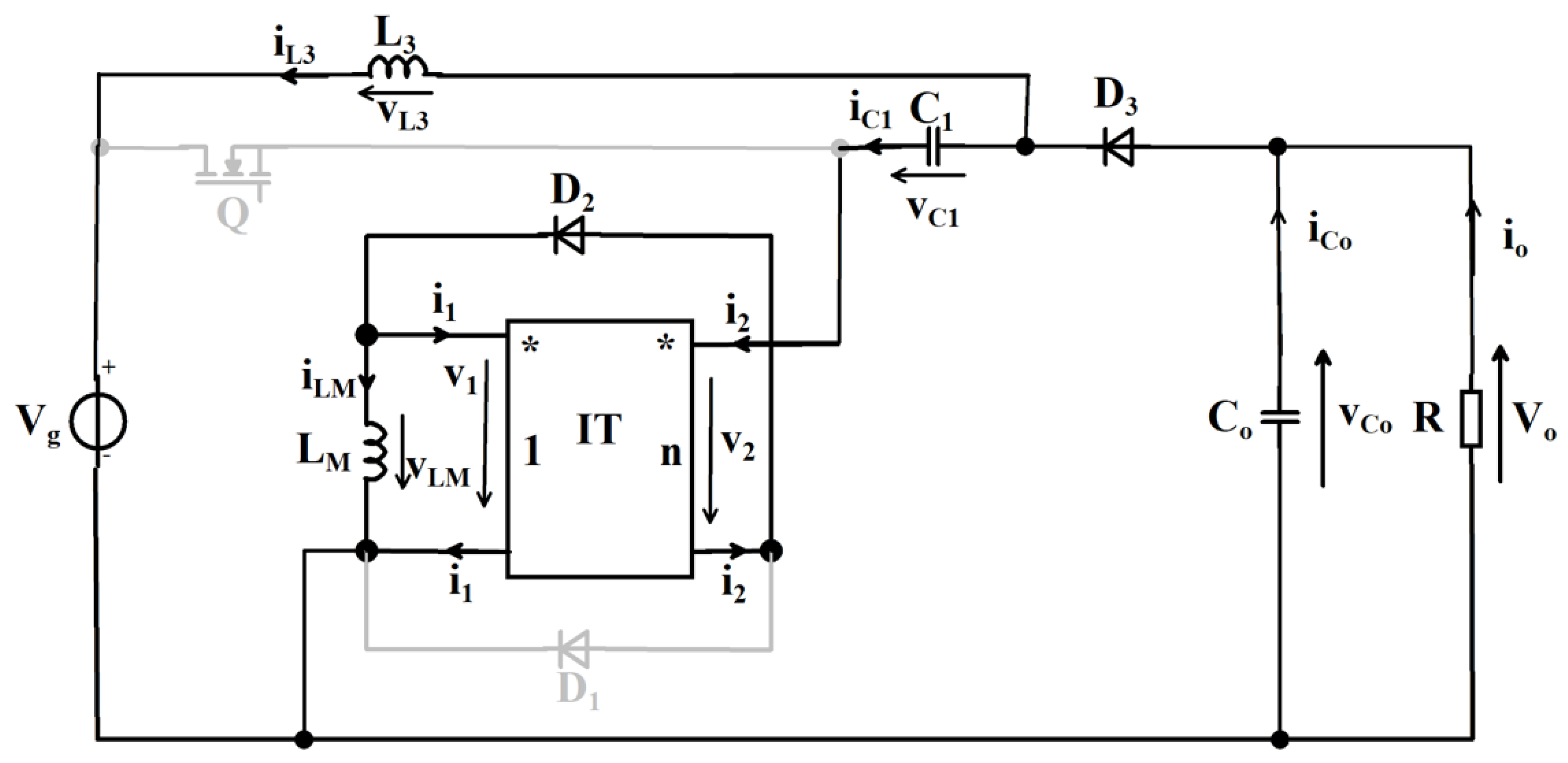
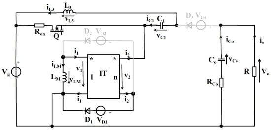
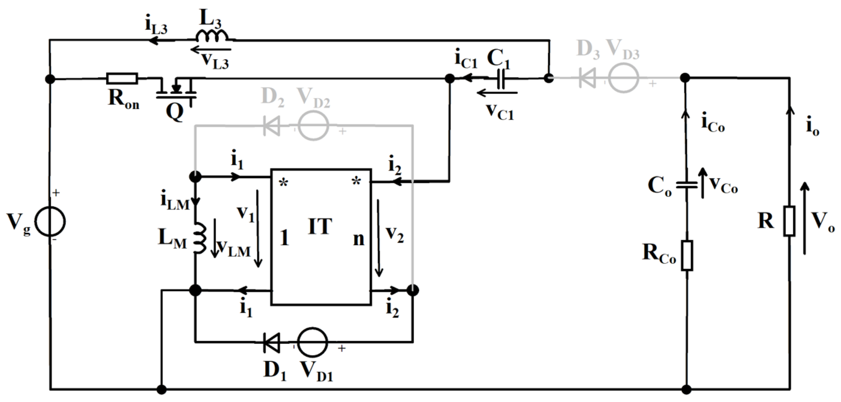
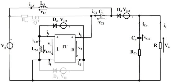
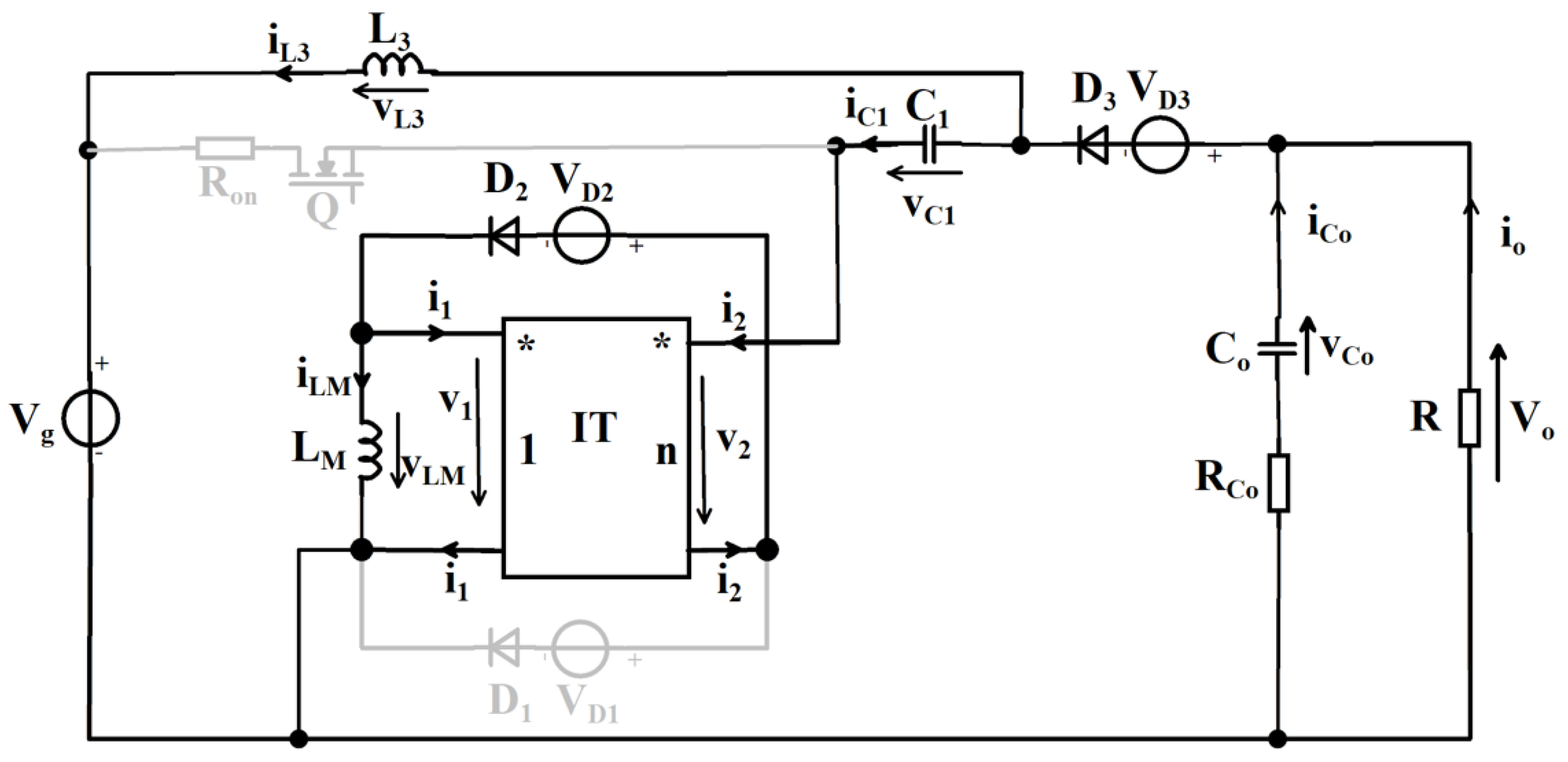
The structure of the proposed converter [42], as seen in Figure 1, contains two perfectly coupled inductors, which are traditionally modeled for analysis by an ideal transformer (IT) together with its corresponding magnetizing inductor, equal to L1, as presented in Figure 2. The turns ratio n = is presumed to be less than unity. It is also easily observed that the presence of only one transistor in the schematic allows the converter control to be performed in a simple manner, by varying only the duty cycle D value, while maintaining a constant switching frequency fs, and switching period Ts, respectively. The continuous conduction mode (CCM) operation is assumed to be valid and, therefore, the converter exhibits two topological states, as seen in Figure 3 and Figure 4. It is remarked that the conduction state of the semiconductor elements depends on the topological state.
Figure 1.
The buck–boost topology proposed in [42].
Figure 2.
The equivalent model of the converter [42].
Figure 3.
Equivalent schematic of the proposed converter [42]—first topological state.
Figure 4.
Equivalent schematic of the proposed converter [42]—second topological state.
The ideal transformer is typically characterized by two equations, as seen below:
Performing traditional dc analysis by invoking volt-second balance and charge balance equations, the expressions of the capacitor dc voltages, inductor dc currents, and static conversion ratio M result as follows:
As mentioned in [42], there are certain duty cycle limits, which depend only on the value of the turns ratio n, that define the behavior of the proposed converter. For proper operation, the duty cycle must not go below . As Equation (4) reveals, a lower turns ratio leads to a higher static conversion ratio than that of a standard buck–boost converter. Moreover, it can be demonstrated that, for a specified n, the duty cycle values exceeding produces a static conversion ratio that is greater than that of the buck–boost topology. Because decreases as n gets smaller, lower turns ratios lead to a more pronounced boosting capability. If the duty cycle is higher than , it can be demonstrated that the static conversion ratio becomes higher than that of the classical boost converter. On the other hand, the proposed topology also has a step-down operating mode for duty cycles lower than . This means that the step-down operating region narrows as the turns ratio n gets lower. The limiting duty cycles satisfy the inequality Dlim1 < Dlim4 < Dlim2 < Dlim3.
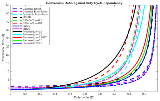
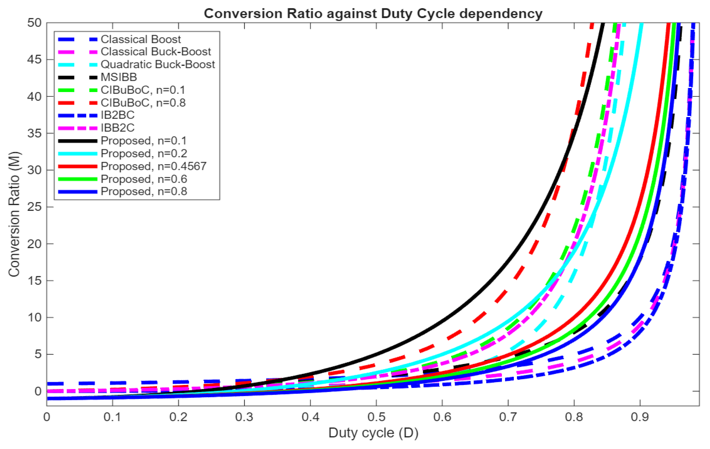
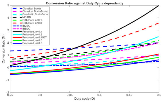
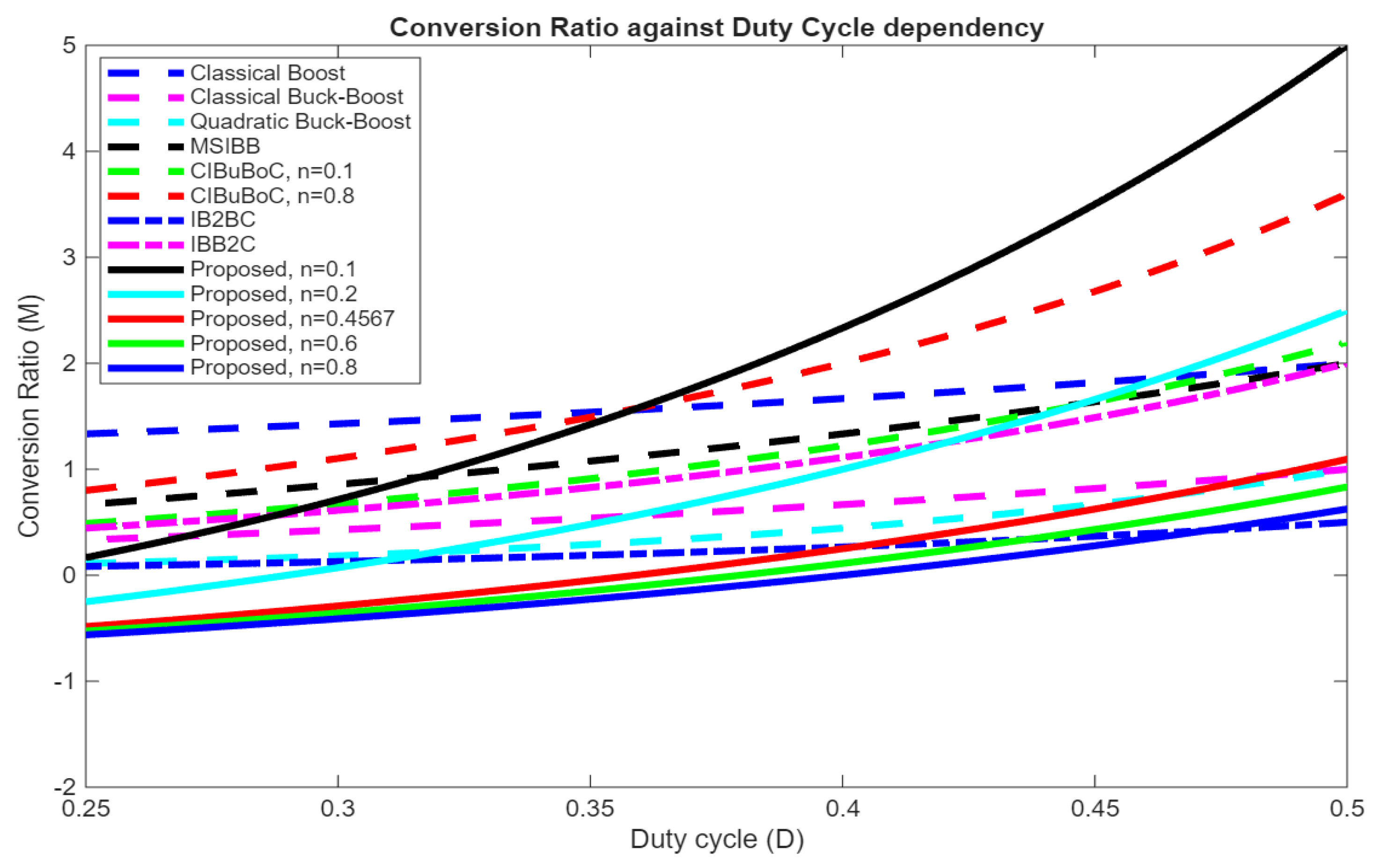
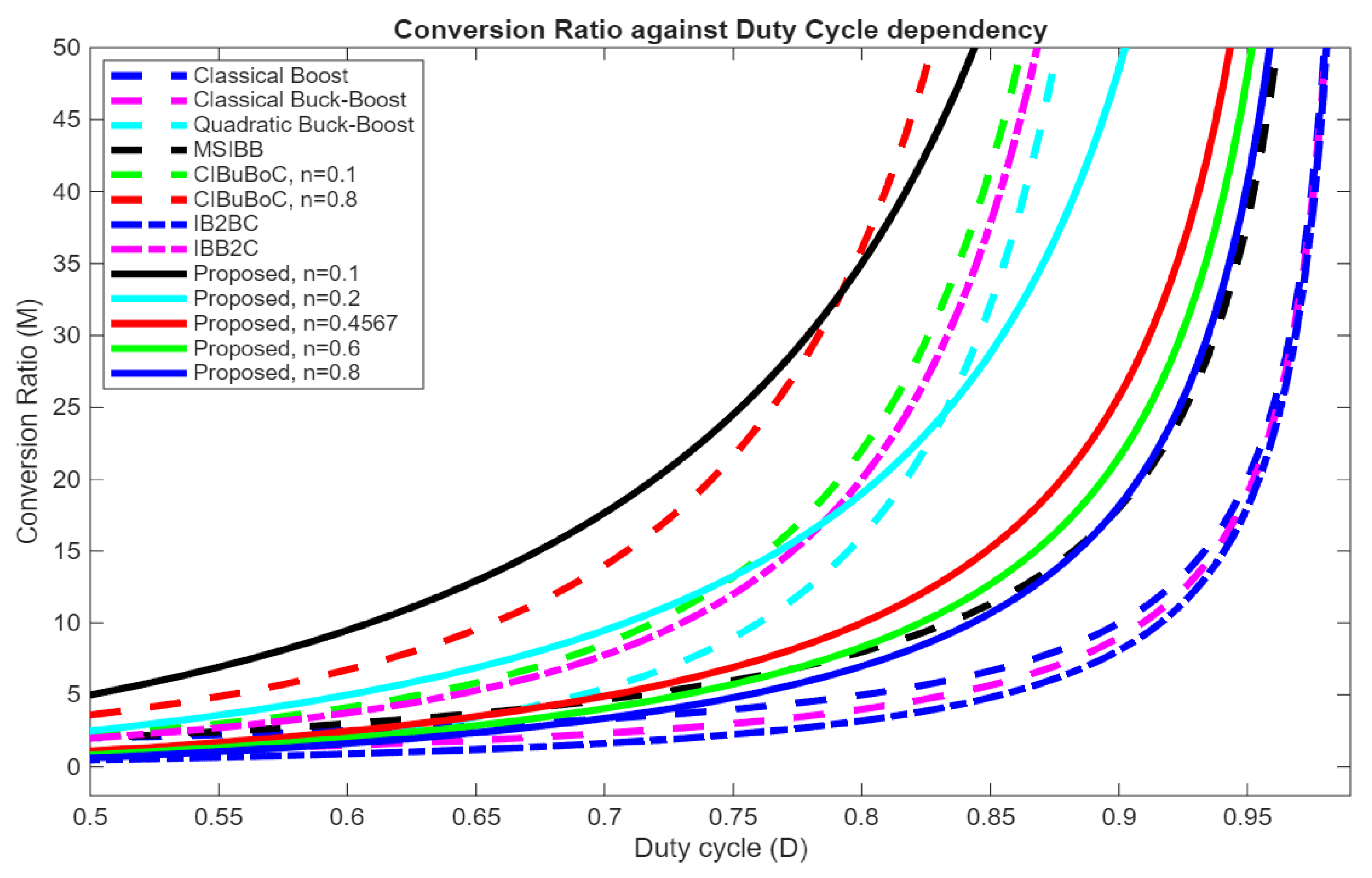
The static conversion ratio comparison performed for several values of the turns ratio n together with the corresponding characteristics of the classical boost [2], classical buck–boost [2], quadratic buck–boost [11], MSIBB [9], CIBuBoC [39], IB2BC [23] and IBB2C [23] converters is depicted in Figure 5, Figure 6 and Figure 7. To enhance visibility of the operating regions, Figure 6 presents the characteristics with limited duty cycles between 0.25 and 0.5, and Figure 7 illustrates the duty cycle range between 0.5 and 0.99.
Figure 5.
Static conversion ratio comparison—graphical representation up to M = 50.
Figure 6.
Static conversion ratio comparison—graphical representation up to M = 5 and with restricted duty cycle range (D between 0.25 and 0.5).
Figure 7.
Static conversion ratio comparison—graphical representation up to M = 50 and with restricted duty cycle range (D between 0.5 and 0.99).
Depending on the value of n, the buck region is different. For example, from Figure 6, it can be observed that for n = 0.1, the proposed converter operates in a step-down regime from approx. D = 0.25 to D = 0.34. This behavior classifies this topology as having the shortest buck region compared to the other converters. As the duty cycle increases (Figure 7), the proposed converter exhibits a smooth transition in conversion ratio, maintaining a predictable, strictly monotonic increasing dependence on both D and n. In this region, the proposed topology demonstrates a more pronounced step-up when the turns ratio n = 0.1 relative to the other converters, and comparable to CIBuBoC [39] when n = 0.8.
Table 1 provides a comparison between the proposed buck–boost converter and the classical boost [2], classical buck–boost [2], quadratic buck–boost [11], MSIBB [9], CIBuBoC [39], IB2BC [23], and IBB2C [23] converters.
Table 1.
Comparison between different converter topologies.
Examining Table 1, it is clear that the advantage of the proposed topology is the need for only one active switch, similar to the classical [2] and quadratic [11] converters. This feature simplifies the control strategy and gate driver circuit when compared to topologies that employ multiple transistors. The proposed topology is a higher-order system than the classical boost [2] and buck–boost [2] converters, the same fourth order with MSIBB [9], IB2BC [23], and IBB2C [23], but lower than the quadratic [11] and CIBuBoC [39]. The proposed solution differs from the classical [2] and quadratic [11] converters in the sense that it exhibits a better conversion ratio and, typically, to buck–boost counterparts, inverted output voltage compared to the input is provided. The comparison indicates that the proposed converter maintains a good balance between circuit complexity and voltage conversion ratio.
In each converter design, the evaluation of current and voltage stresses on the transistor and diodes has a major impact on the selection of the semiconductor devices. Due to their great importance, the stresses are expressed by using (2), (3), (5), and (6):
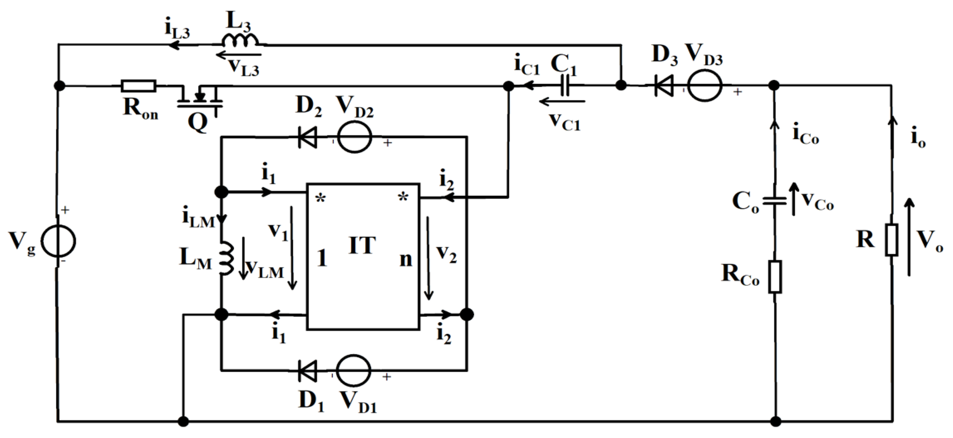
In practical implementations, it usually happens that in the region where step-up converters have a high voltage gain, they exhibit a totally different behavior compared to the ideal case due to the unavoidable presence of conduction and switching losses. Therefore, since the proposed buck–boost converter has a relatively wide duty cycle range where its step-up character is prominent, the analysis of the circuit in the presence of losses is of utmost importance. The considered losses, as depicted in Figure 8, are those introduced by the on-resistance (Ron) of the transistor, the forward voltage drops of the diodes (VD1, VD2, VD3), and also the one from the output capacitor (RCo). The analysis of the lossy converter is based on the state-space approach, where the input vector is chosen to be , while the state vector and the output vector are and respectively. Continuous conduction mode (CCM) operation is assumed, that is, the converter cycles through two distinct topological states.
Figure 8.
The proposed buck–boost converter, with losses.
Based on Figure 9, the state matrices corresponding to the first topological state are:
Figure 9.
The first topological state of the proposed buck–boost converter, with conduction losses.
According to Figure 10, the resulting state matrices corresponding to the second topological state, where , are:
Figure 10.
The second topological state of the proposed buck–boost converter, with conduction losses.
Applying the averaging operator in order to get a dc steady-state operation, the dc value of the output vector, in this case Vo, is obtained by applying the well-known formula [2]:
where the matrices AD, BD, ED, and FD are:
Equations (17) and (18) are typical for dc analysis of two state topologies, being the same for any converter. By using (17), the expression of the lossy static conversion ratio, which is the ratio between the output and input voltages (Vo/Vg), is calculated as follows:
Knowing the averaged state matrices, written in (18), the control-to-output transfer function of the proposed topology, denoted by GC, is obtained after linearizing the state-space equations around a dc constant steady-state operating point. It results in:
where I is the fourth-order unity matrix and:
The results in (20) and (21) are well-known and general, their formalism being the same for any DC–DC CCM-operated converter. The difference is made only by the state matrices.
The converter design is performed while considering the design parameters summarized in Table 2. Using the design equations provided in [42], the resulting component values are presented in Table 3.
Table 2.
Design parameters.
Table 3.
Component values.
The 100 kHz switching frequency is chosen high enough to get a compact and small converter, but low enough such that the switching losses can be neglected compared to the conduction ones, as the analysis was performed taking into account only the conduction losses.
The transformer ratio is chosen such that the converter operates at a reasonable duty cycle. In this case, the duty cycle was chosen to be 0.6986.
The losses are given by the semiconductor devices, which are selected based on their respective current and voltage stresses. Therefore, the chosen transistor is FDP083N15A, while all of the diodes are MURF1660CT. Looking at the datasheets, the transistor on-resistance is Ron = 8.3 mΩ and the diodes forward voltage drops are VD1 = VD2 = VD3 = 1.5 V. The equivalent series resistor (ESR) of the output capacitor is considered to be 50 mΩ. The inductors were manufactured in the laboratory.
Using the component values and the input-output parameters that were imposed for the design, the numerical expression of the control-to-output transfer function is determined to be:
The poles, and zeros, of the control to output transfer function are:
It can be easily seen that the control transfer function is of fourth order with two pairs of left-half plane (LHP) complex conjugate poles, one LHP zero, and three right-half plane (RHP) zeros.
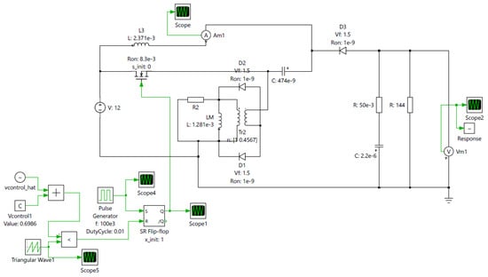
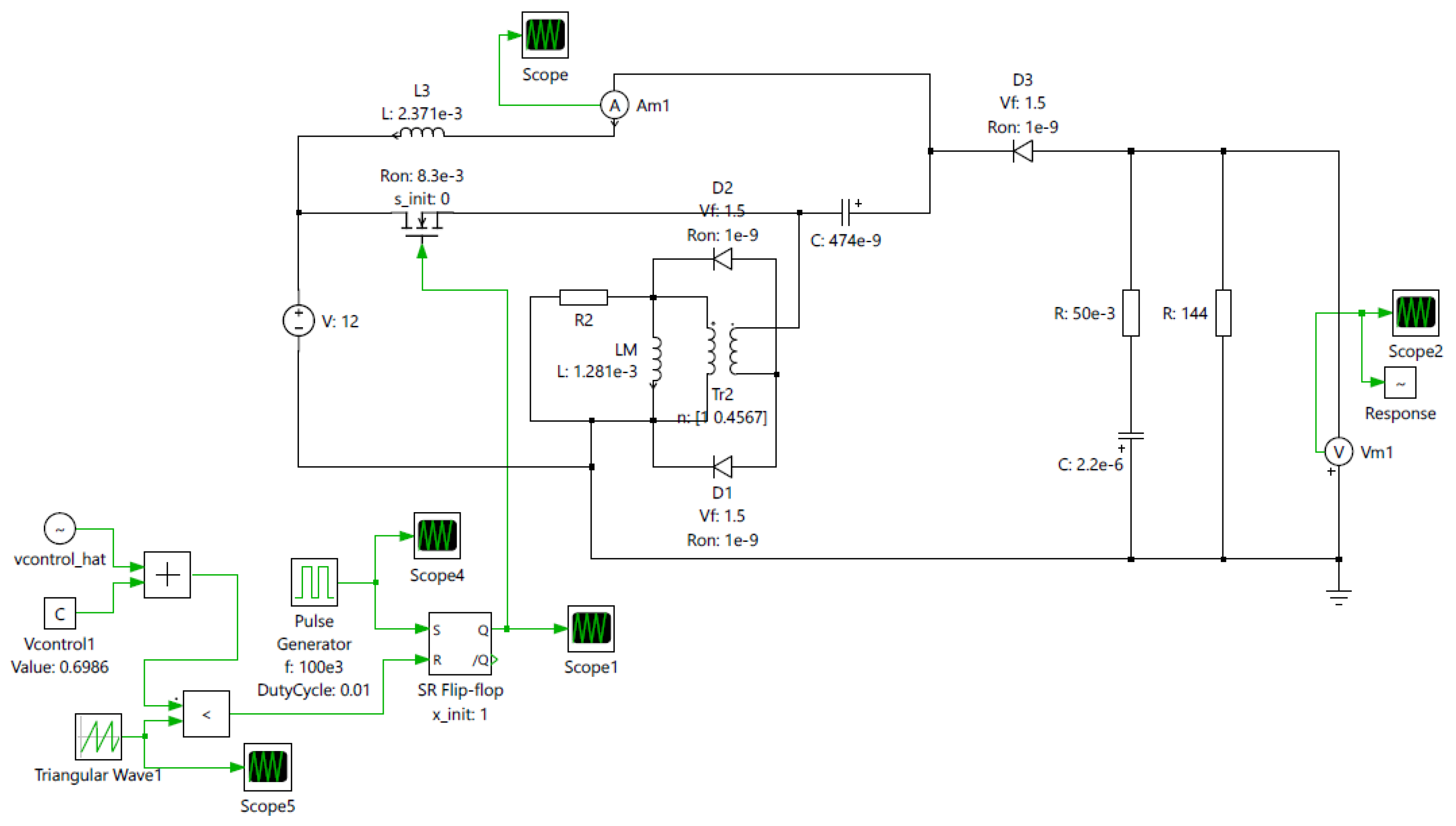
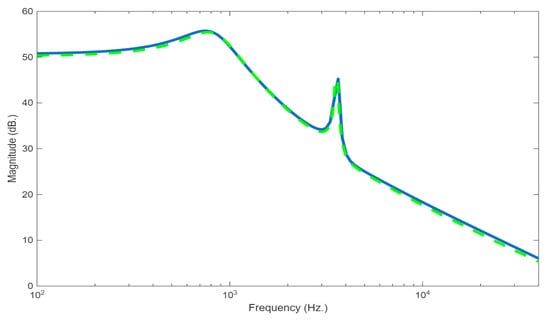
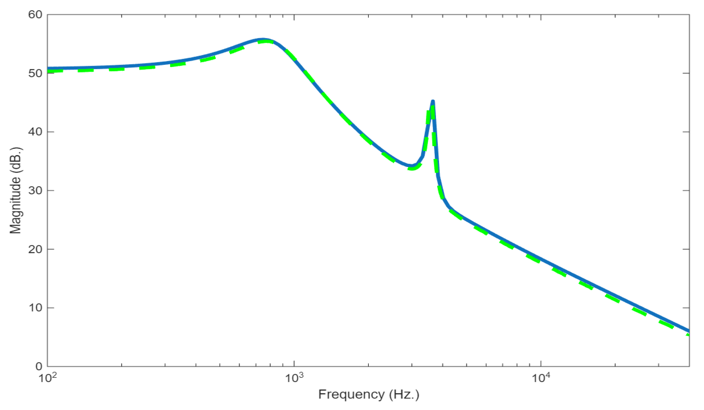
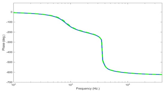
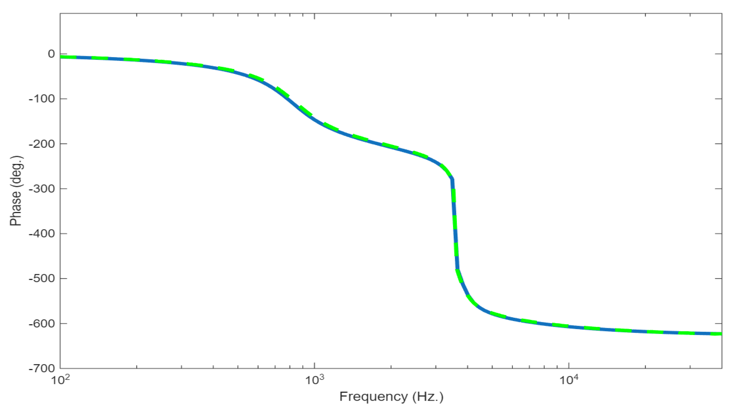
To validate the analytical Expression (22) of the open-loop control-to-output transfer function obtained in MATLAB 2025a [43], the proposed converter is also simulated using the PLECS simulation tool v5.0.1 [44], which provides an AC sweep analysis functionality and generates the Bode plots of the required transfer function. The converter schematic created in PLECS is depicted in Figure 11. The Bode plots obtained from the PLECS simulation and those resulting from MATLAB are compared in Figure 12 and Figure 13, where it can be observed that both the magnitude and phase characteristics are overlaid, thus validating the theoretical considerations.
Figure 11.
PLECS simulation schematic of the proposed converter.
Figure 12.
Comparison between magnitude characteristics—result from transfer function (blue) and AC sweeping (dashed green).
Figure 13.
Comparison between phase characteristics—result from transfer function (blue) and AC sweeping (dashed green).
In the design of the controller, the type III error amplifier is still an adequate choice despite the higher converter order. From [45], considering an ideal type III amplifier, the typical formula of its transfer function is written as follows:
The design parameters, corresponding to the error amplifier, result after invoking the use of an analytical technique based on the system poles and zeros, usually known as the pole-zero placement method. Similar to the buck–boost and boost converters, the presence of the RHP zeros restricts the cut-off frequency. As is known, the type III amplifier exhibits two LHP poles and two LHP zeros. The zeros are chosen to cancel the first two pairs of conjugate poles, , while one pole is equal to , and the other is placed at half of the switching frequency. The cutoff frequency of 300 Hz is chosen according to the rules provided in [45,46]. A phase margin equal to 60 degrees is adopted, and the calculation of the component values that are part of the error amplifier is performed in MATLAB [43]. The results obtained are, the notations being those of [45]:
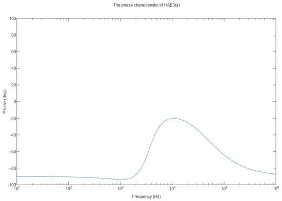
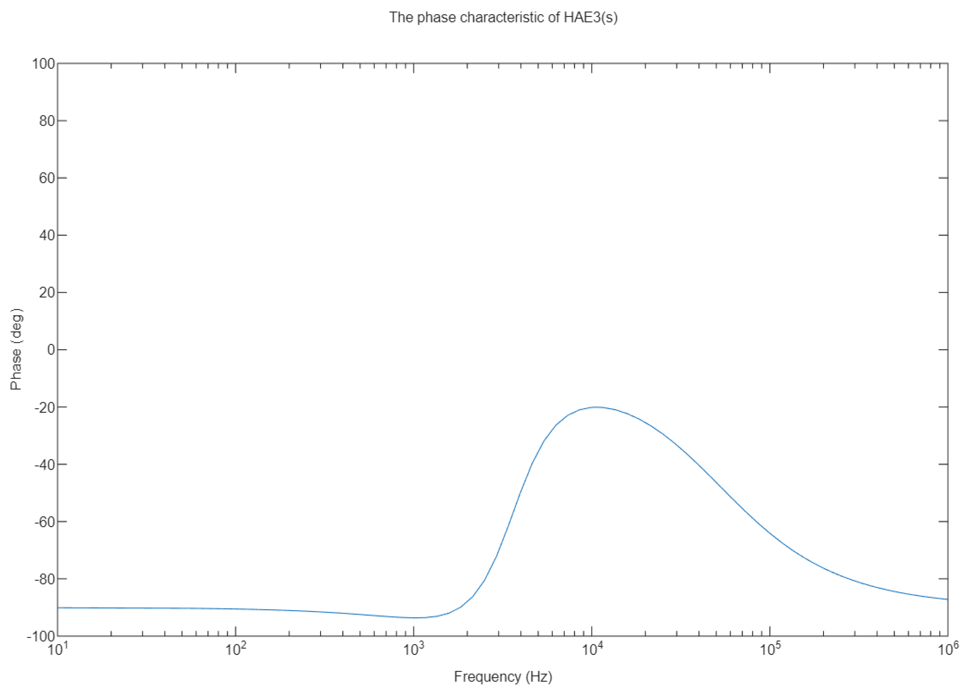
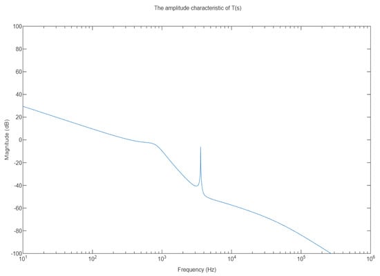
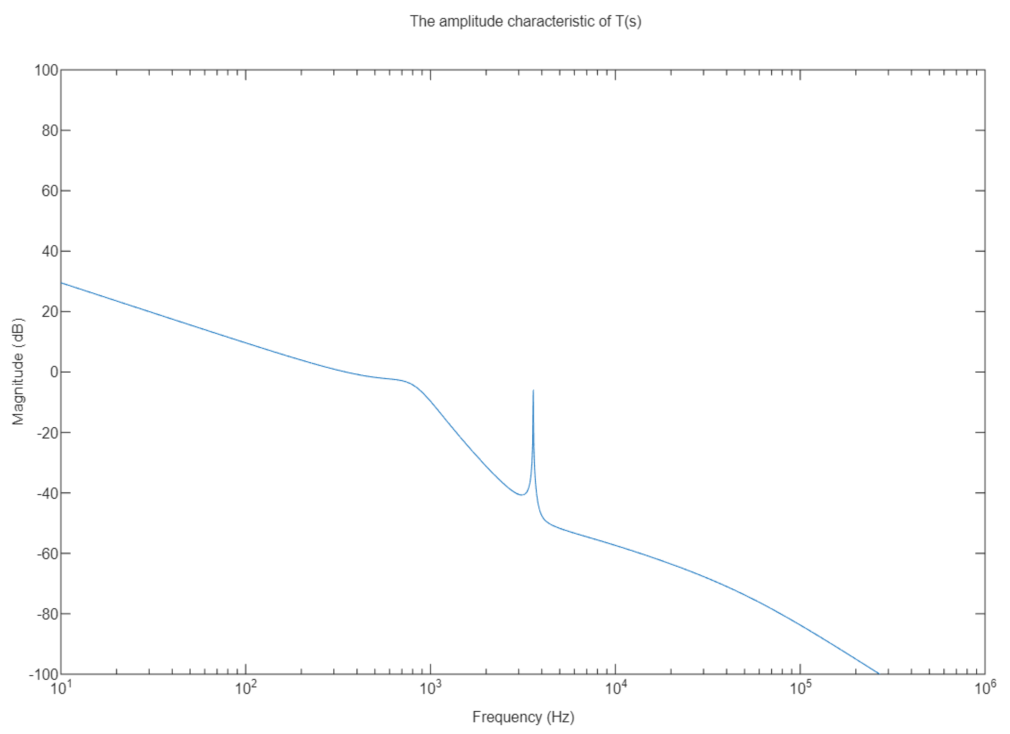
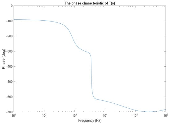
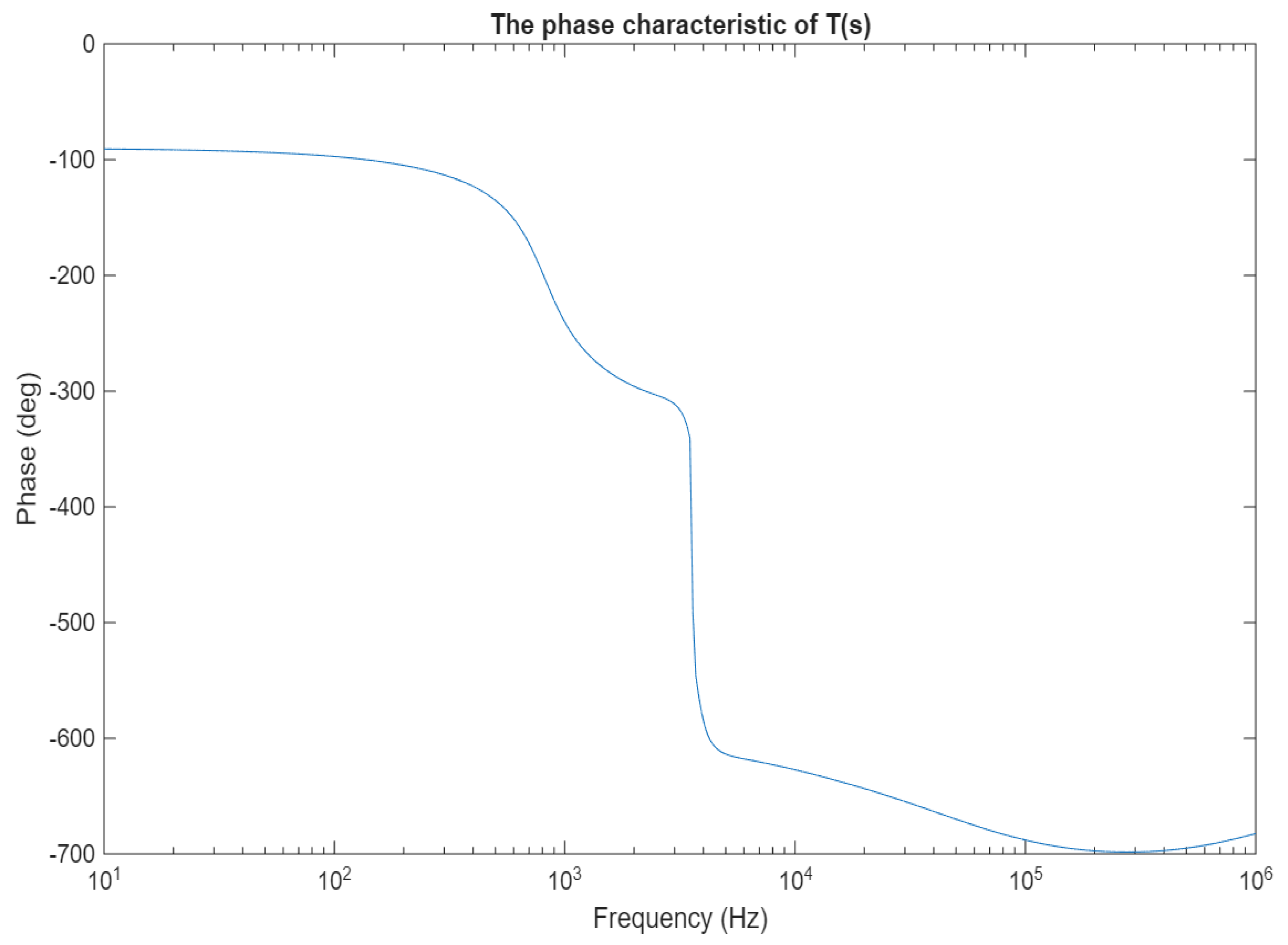
Figure 14 illustrates the magnitude characteristic of the error amplifier for the selected parameter values, whereas Figure 15 shows its phase characteristic. The magnitude characteristic of the open-loop transfer function is shown in Figure 16, while the corresponding phase characteristic is presented in Figure 17.
Figure 14.
Error amplifier—magnitude characteristic obtained in MATLAB.
Figure 15.
Error amplifier—phase characteristic obtained in MATLAB.
Figure 16.
Open-loop transfer function—magnitude characteristic obtained in MATLAB.
Figure 17.
Open-loop transfer function—phase characteristic obtained in MATLAB.
As seen from the graphical representation above, the actual crossover frequency is 347.6279 Hz, and the resulting phase margin is 62.3304 degrees.
3. Results
The simulations of the proposed converter, as well as the experimental part, are performed while considering the design parameters mentioned above.
3.1. Simulation Results
3.1.1. Open-Loop Simulation
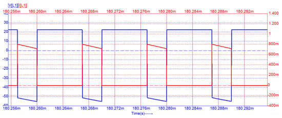
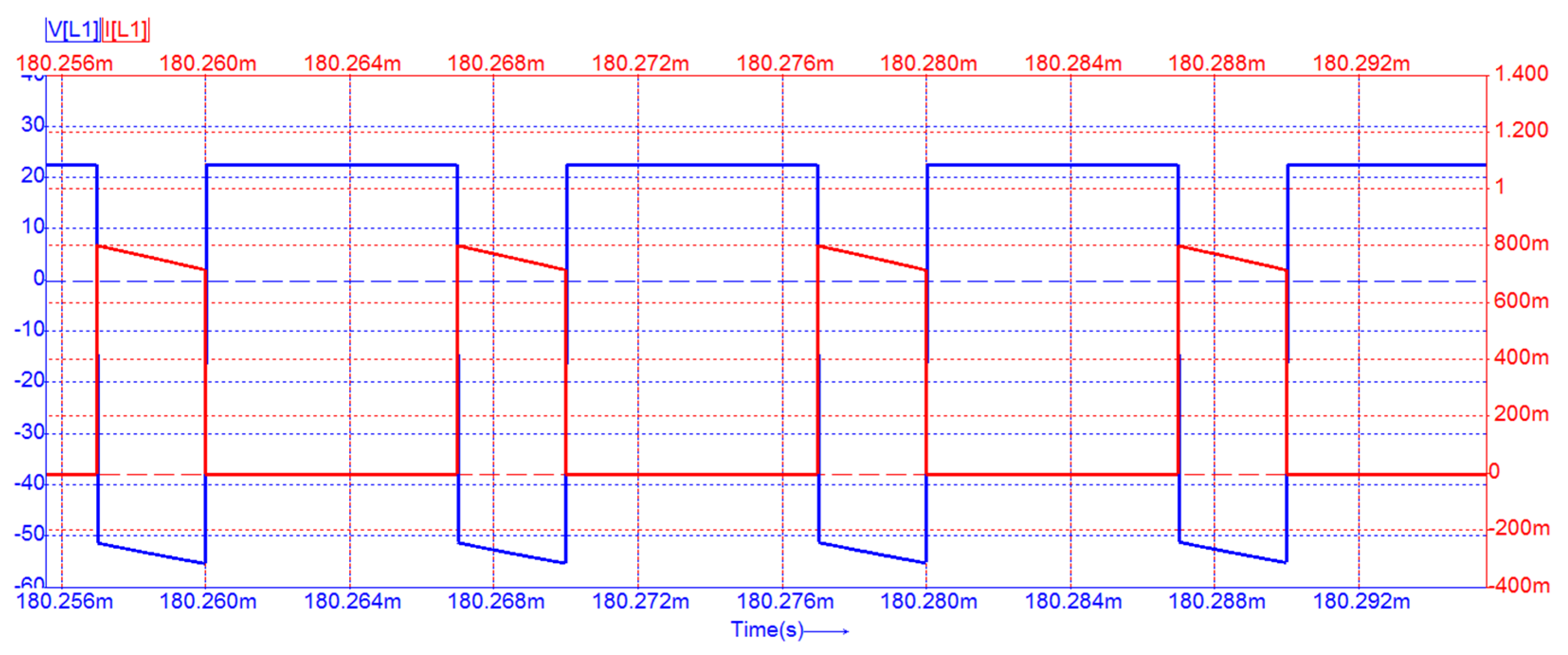
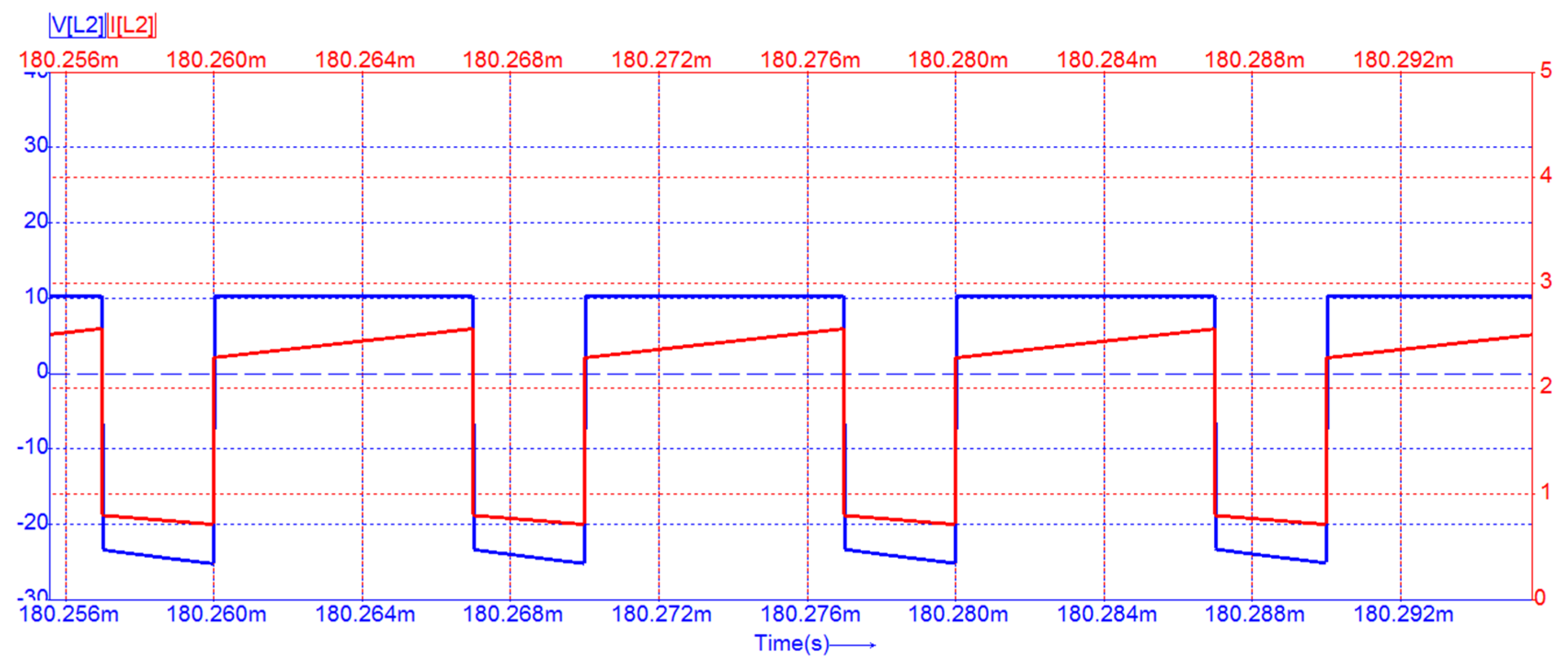
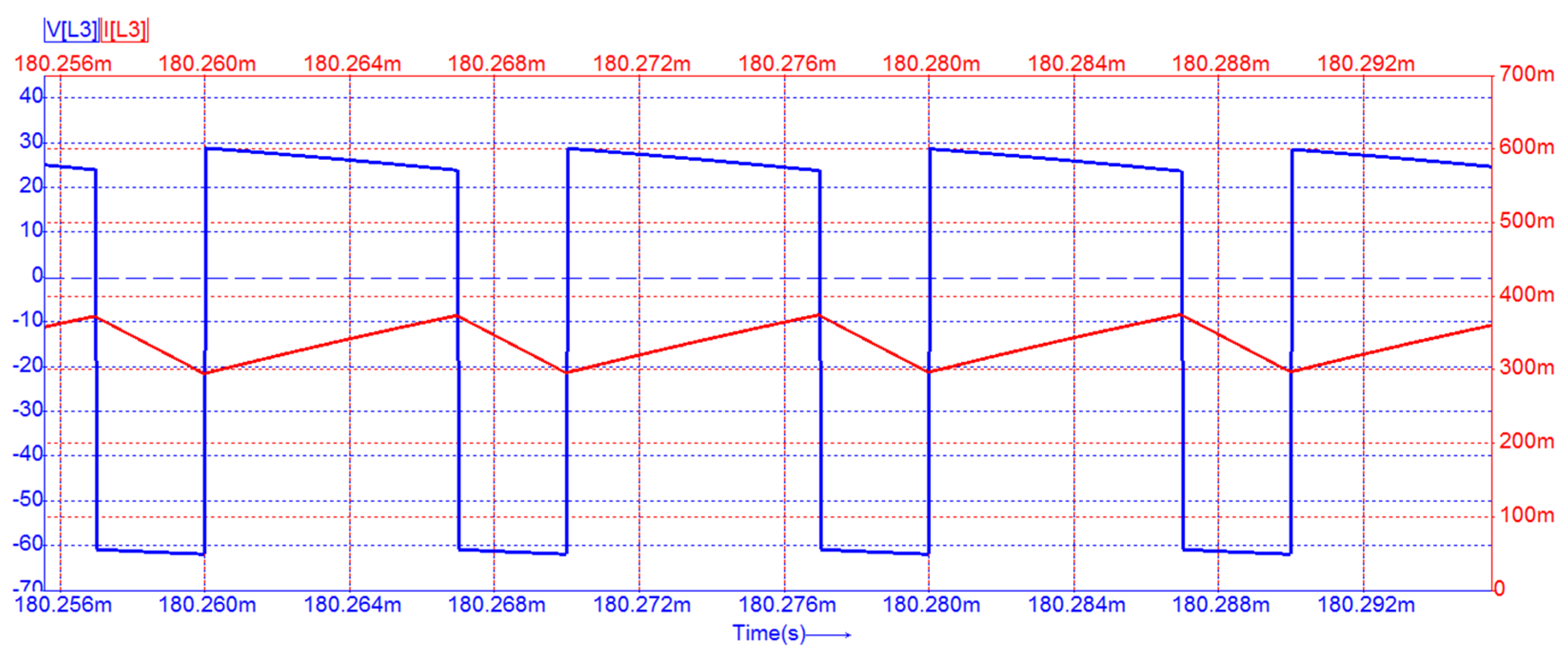
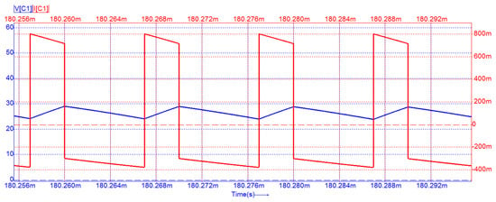
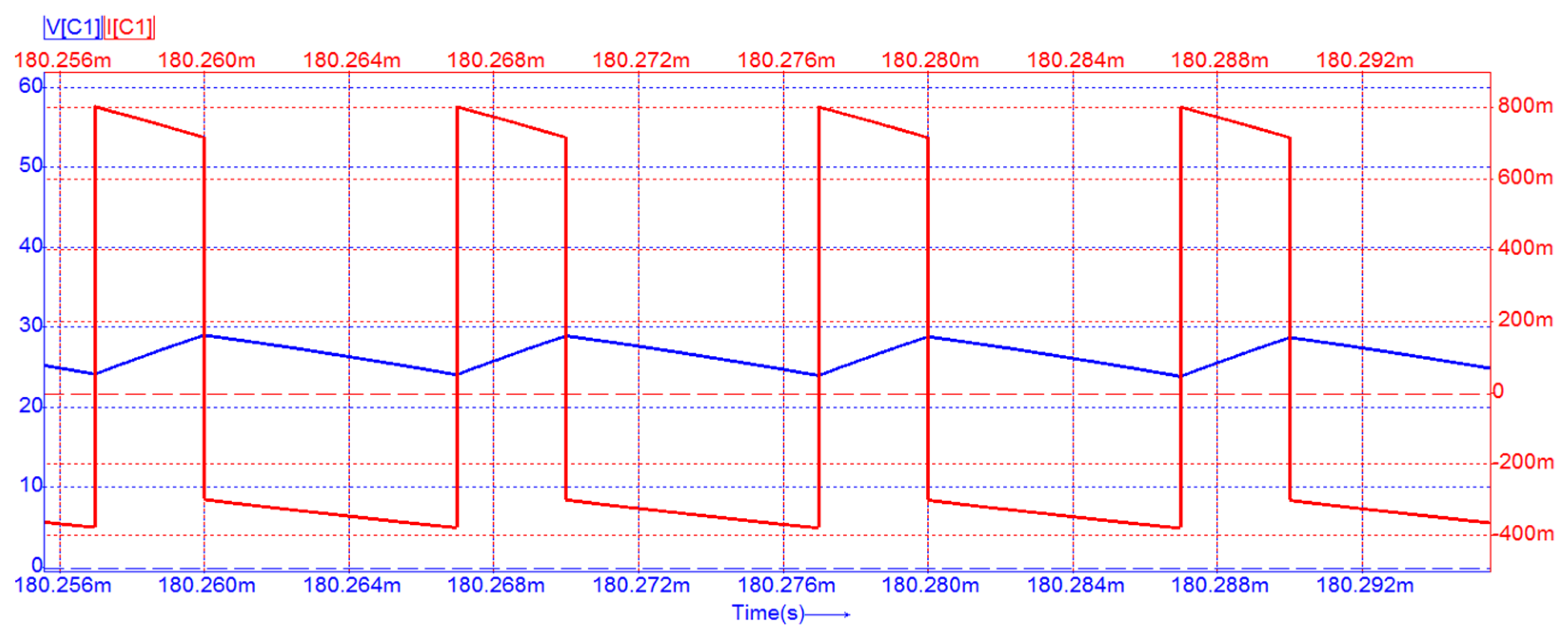
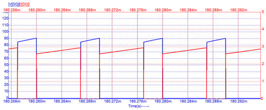
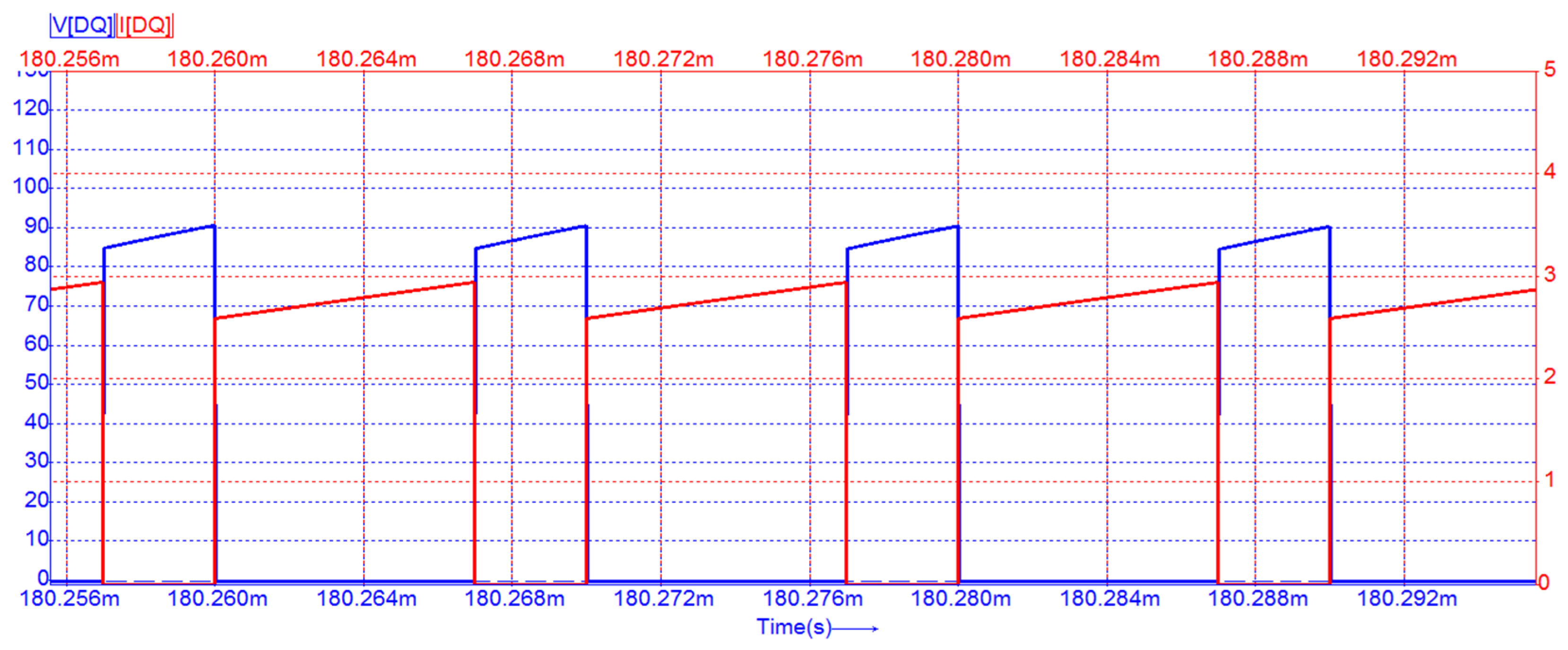
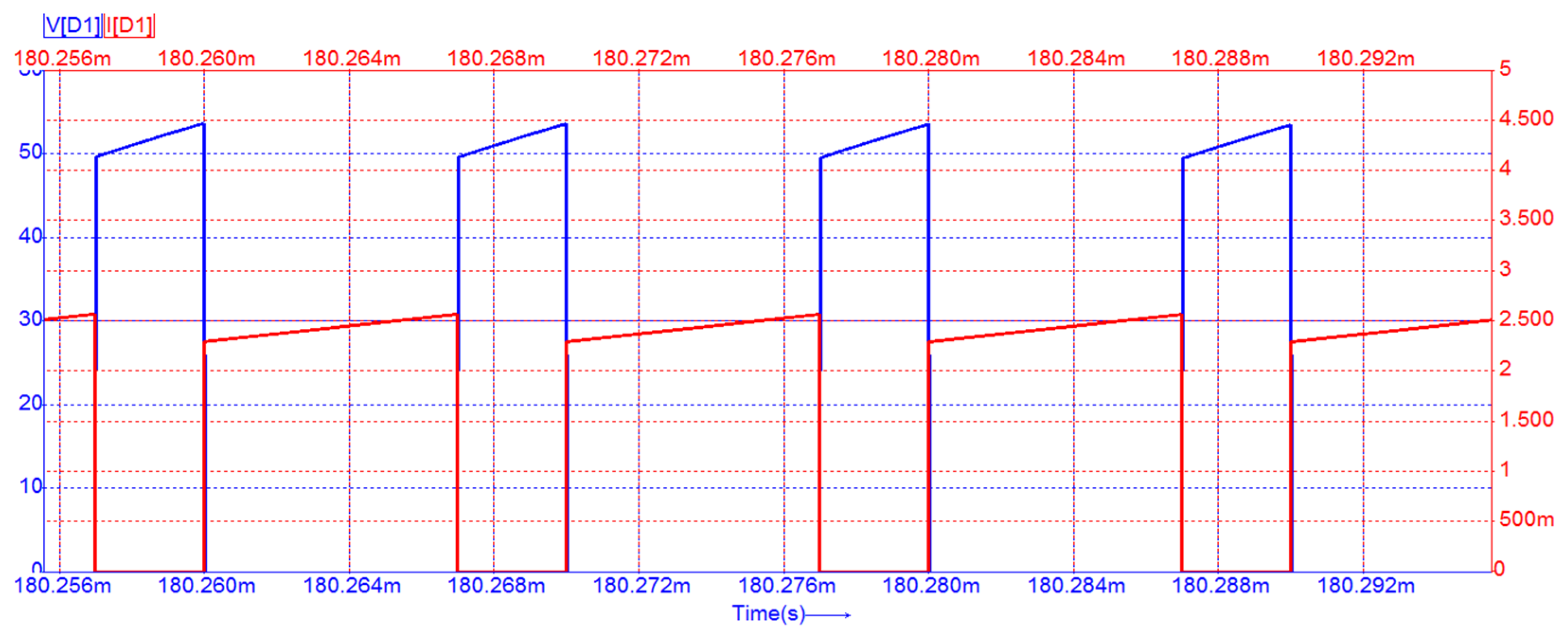
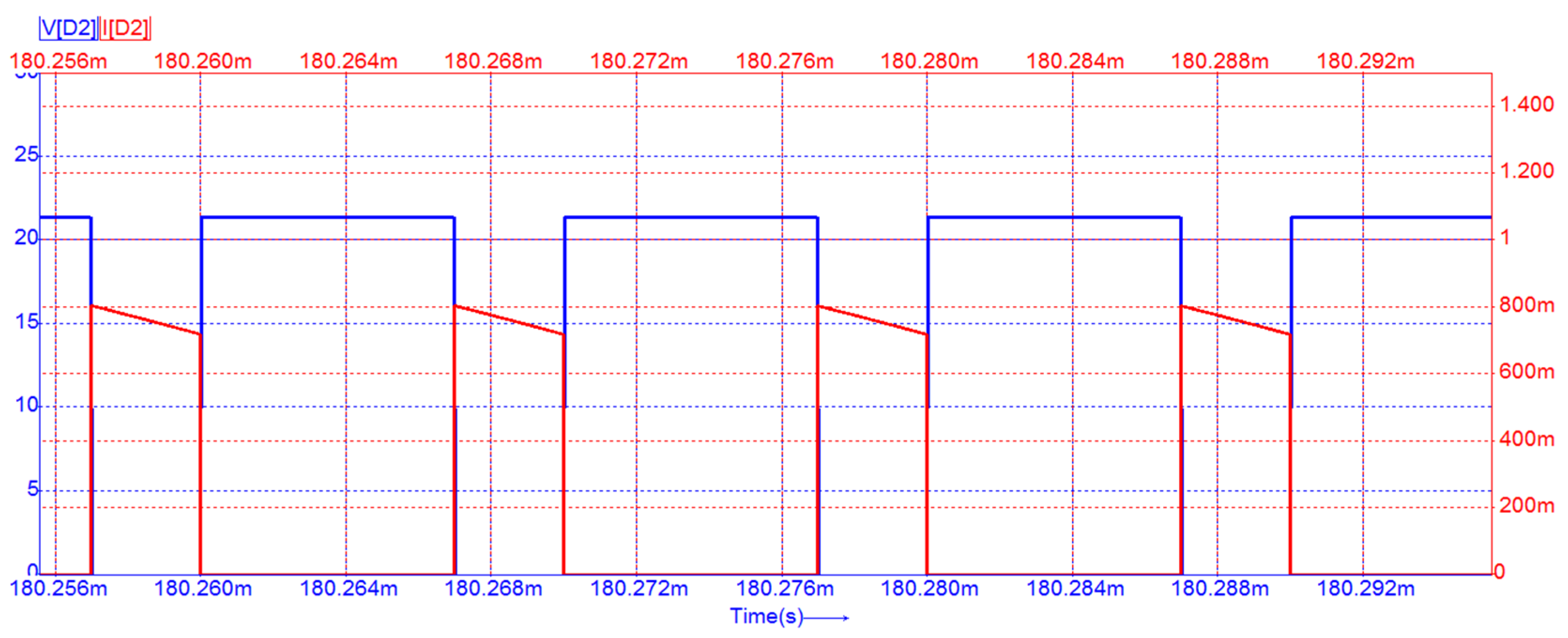
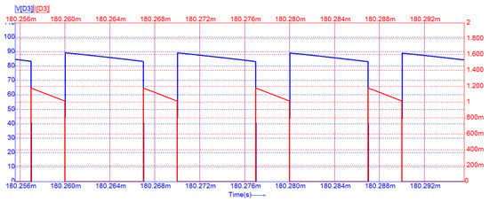
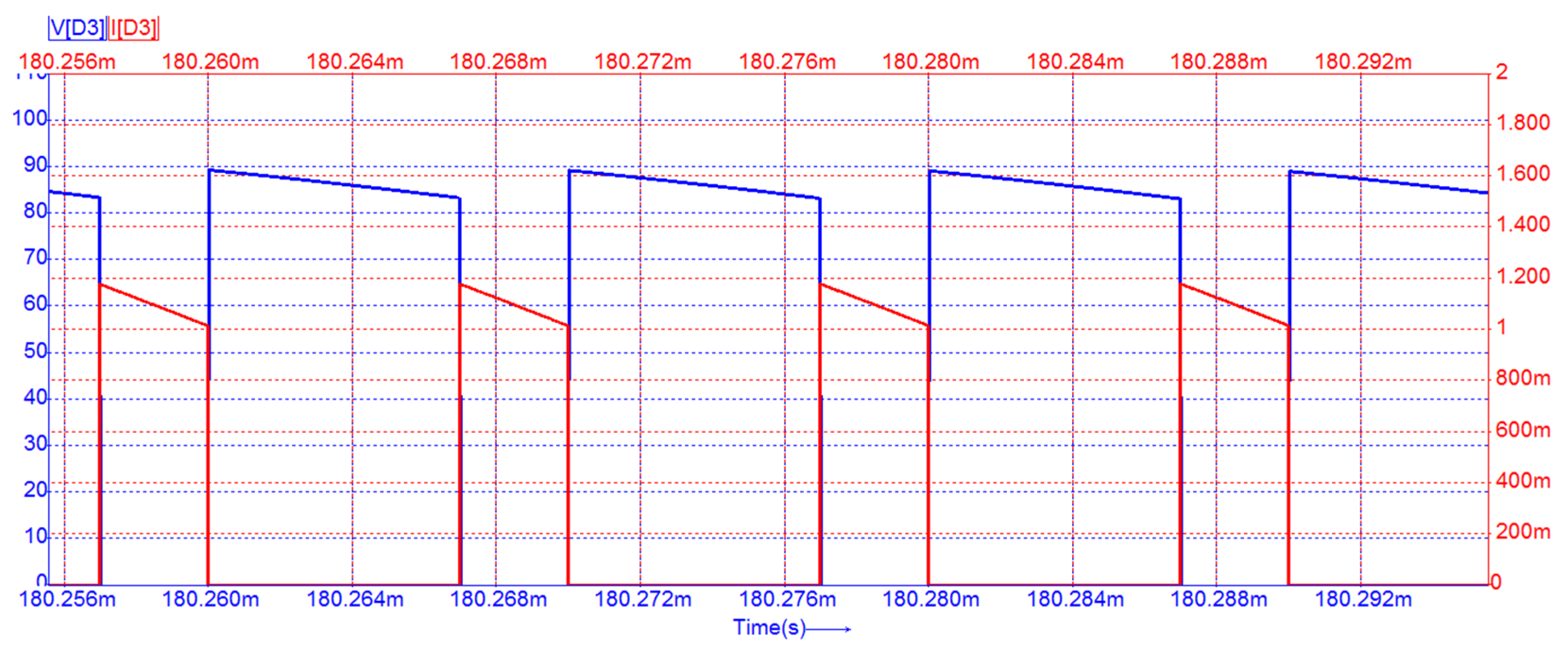
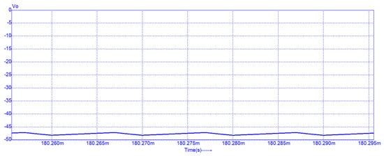
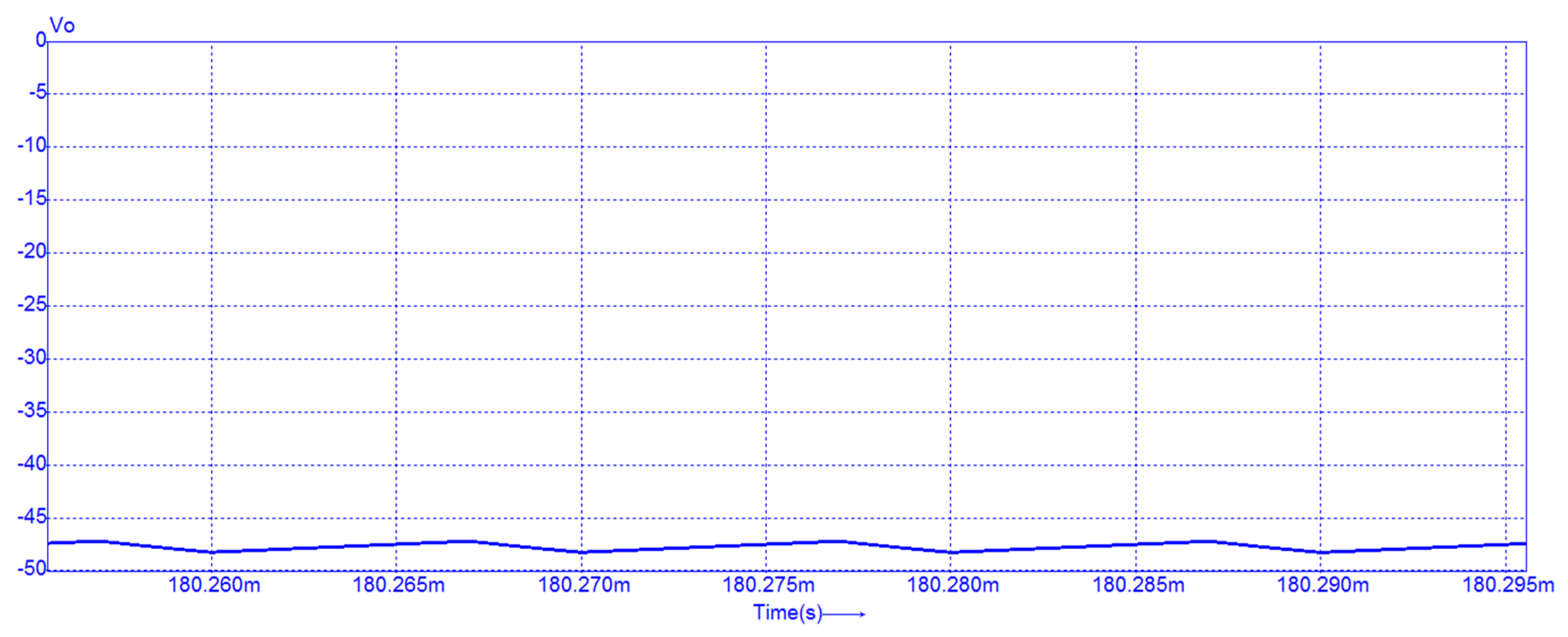
The lossy converter was simulated using the CASPOC 2017 package [47], and the simulation results are shown in Figure 18, Figure 19, Figure 20, Figure 21, Figure 22, Figure 23, Figure 24, Figure 25 and Figure 26. The same parameters as those adopted in the previous section are used. As a convention, the currents are represented in red, while the waveforms of the voltages are depicted in blue.
Figure 18.
Converter with losses (open loop)—voltage and current corresponding to L1.
Figure 19.
Converter with losses (open loop)—voltage and current corresponding to L2.
Figure 20.
Converter with losses (open loop)—voltage and current corresponding to L3.
Figure 21.
Converter with losses (open loop)—voltage and current corresponding to C1.
Figure 22.
Converter with losses (open loop)—voltage and current corresponding to transistor Q.
Figure 23.
Converter with losses (open loop)—voltage and current corresponding to diode D1.
Figure 24.
Converter with losses (open loop)—voltage and current corresponding to diode D2.
Figure 25.
Converter with losses (open loop)—voltage and current corresponding to diode D3.
Figure 26.
Converter with losses (open loop)—output voltage.
All simulations were performed with a duty cycle of 0.69891, slightly higher than the duty cycle of 0.66967 in the ideal case, as expected. It can be remarked that qualitatively, the main waveforms remain unchanged.
3.1.2. Closed-Loop Simulation
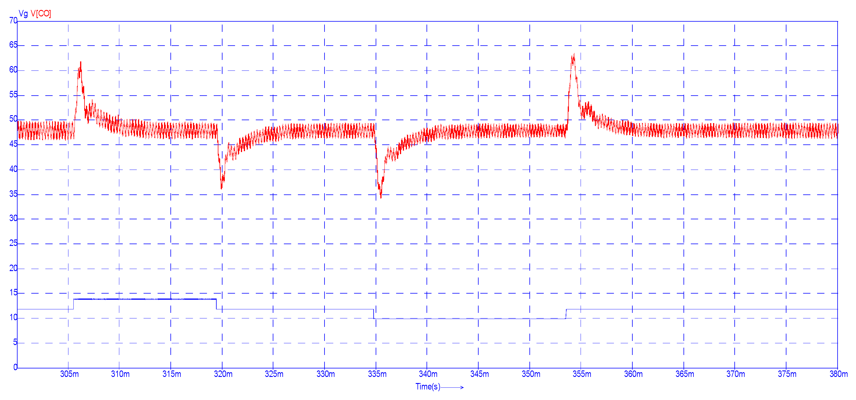
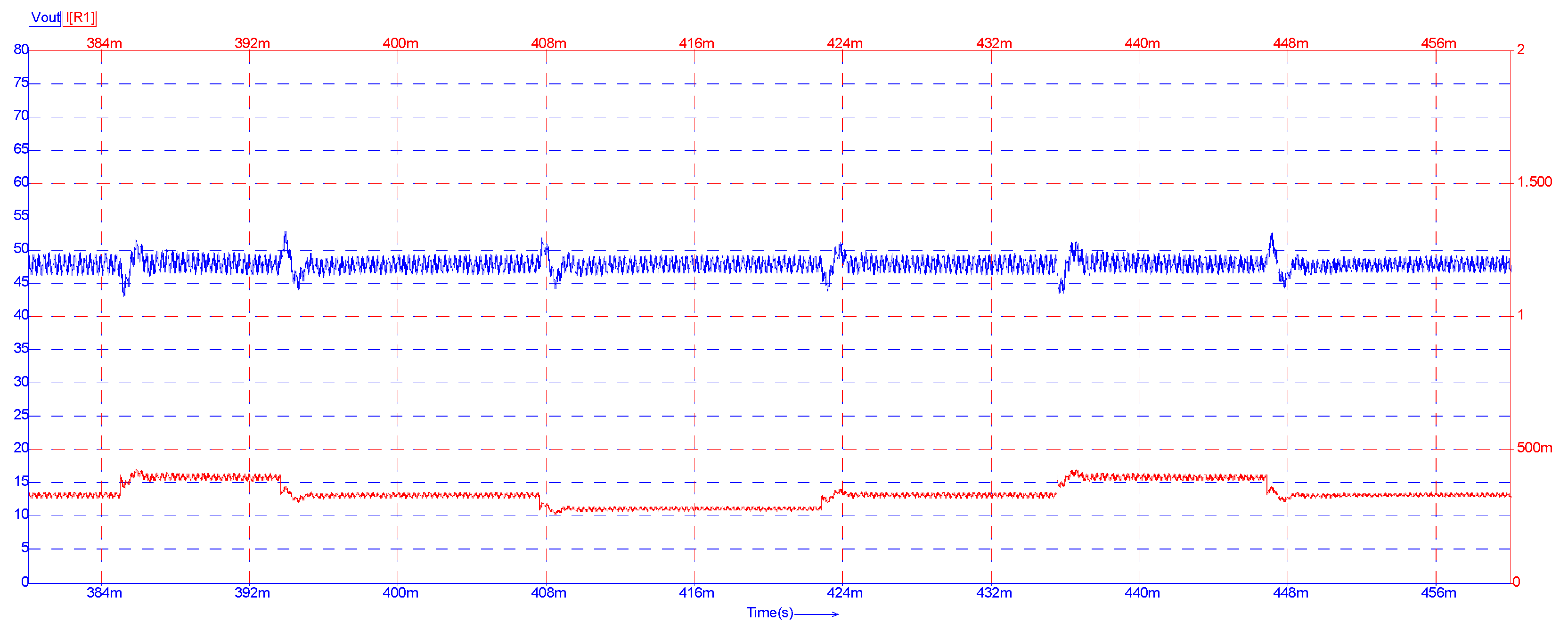
The waveforms corresponding to the proposed topology remain the same as in the case of the open-loop converter. Additionally, in the case of closed-loop simulation, the dynamic response to a step change in the input voltage is shown in Figure 27, while the load resistance is shown in Figure 28.
Figure 27.
Dynamic response to step variation in the input voltage, showing the output (red) and the input (blue) voltage.
Figure 28.
Dynamic response to step variation in the load resistance showing the output voltage (blue) and the output current (red).
In the simulation, for both figures, the print interval is 100 simulation time steps. In Figure 27, the input voltage changes from 12 V to 14 V–12 V–10 V–12 V. It can be observed that, following the transient intervals, the output voltage is successfully regulated to the nominal value of 12 V with moderate overshoot, as specified in the design requirements. The step changes in the load resistance, from Figure 28, show how the converter reacts when the load resistance is modified from the set value of R = 144 Ω. The load is changed from 144 Ω to 120 Ω–144 Ω–170 Ω–144 Ω–120 Ω and back to 144 Ω. The output voltage exhibits good regulation.
3.2. Experimental Results
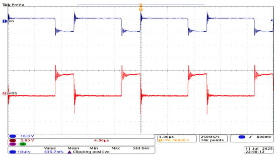
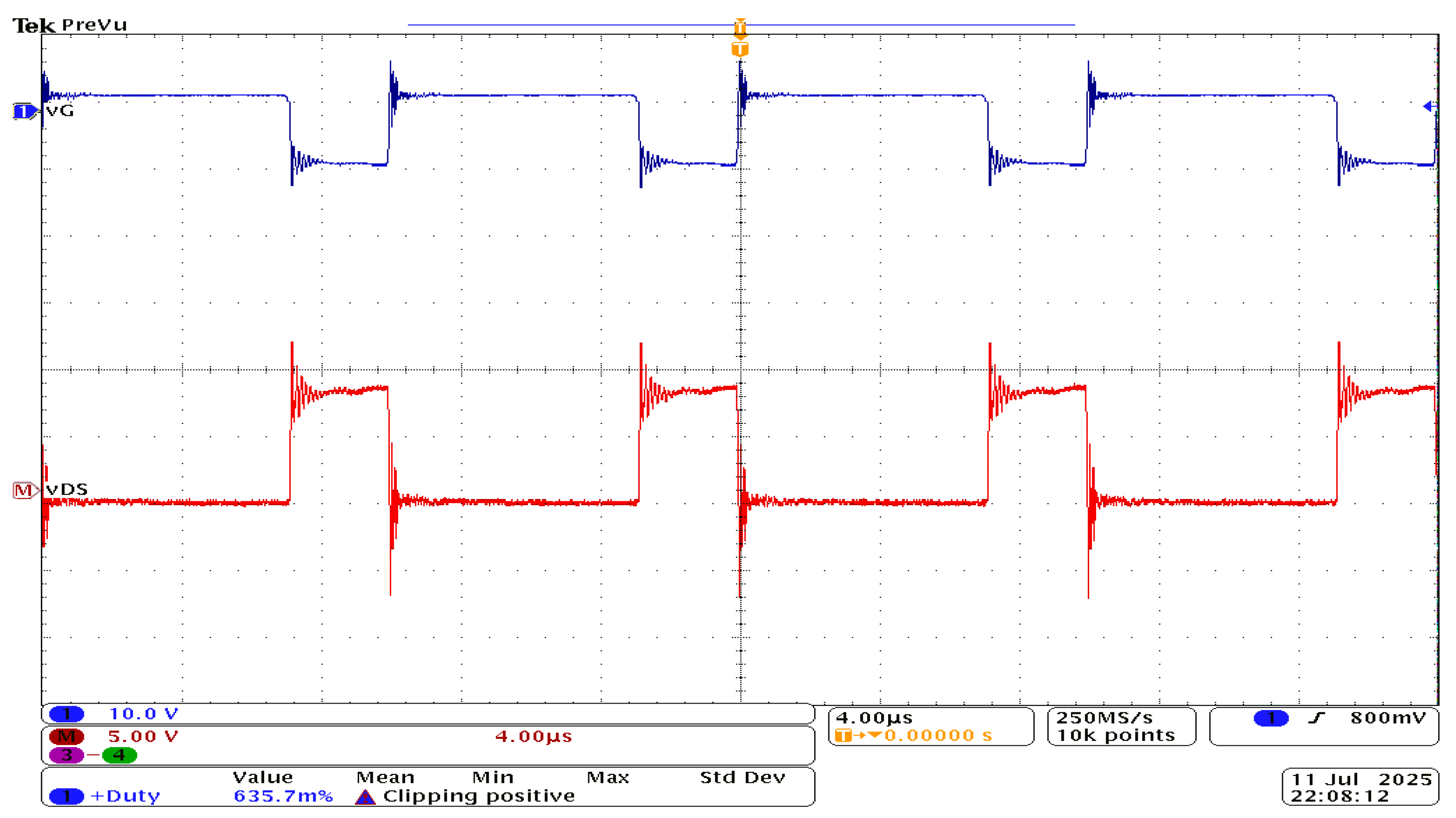
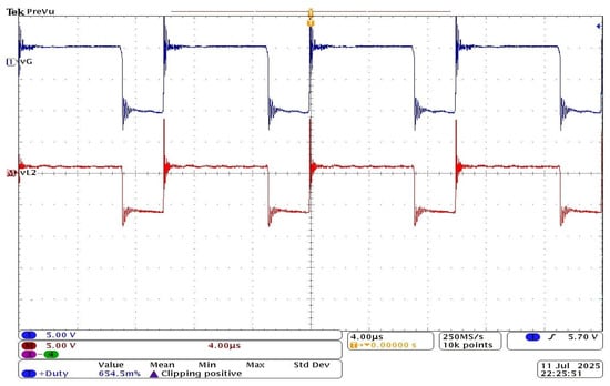
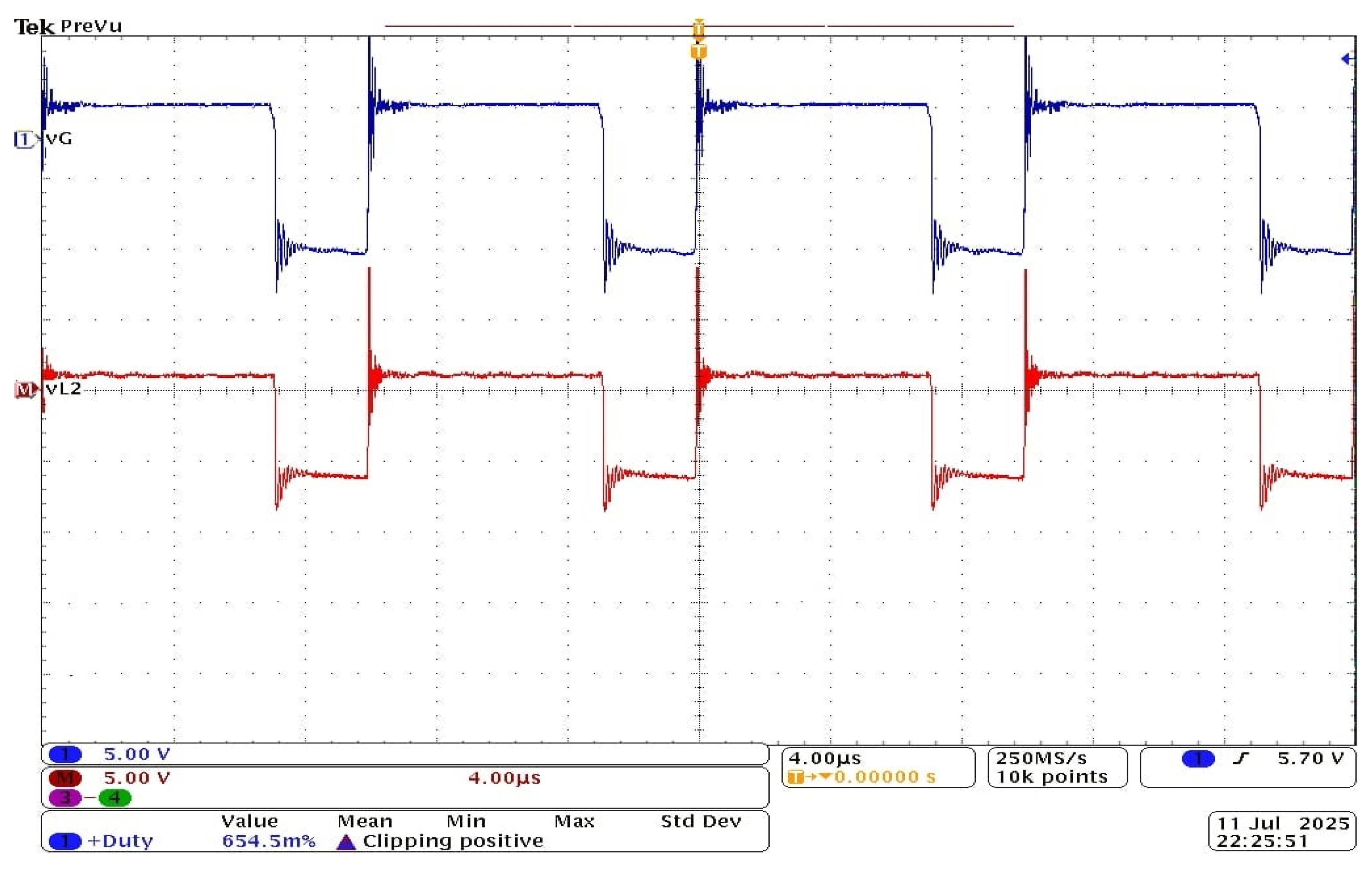
As mentioned beforehand, the component values and design parameters specified at the beginning of Section 2 are being used not only in the simulation, but also in the experimental part. The waveforms acquired from the oscilloscope are presented in Figure 29, Figure 30, Figure 31 and Figure 32, where the transistor gate voltage is considered as a reference signal.
Figure 29.
Experimental waveforms: vG—transistor gate voltage against supply ground (reference signal, acquired with attenuation of 10, represented with dark blue), vDS—transistor drain to source voltage (red).
Figure 30.
Experimental waveforms: vG—transistor gate voltage against supply ground (reference signal, represented with dark blue), vL2—voltage corresponding to inductor L2 (red).
Figure 31.
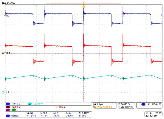
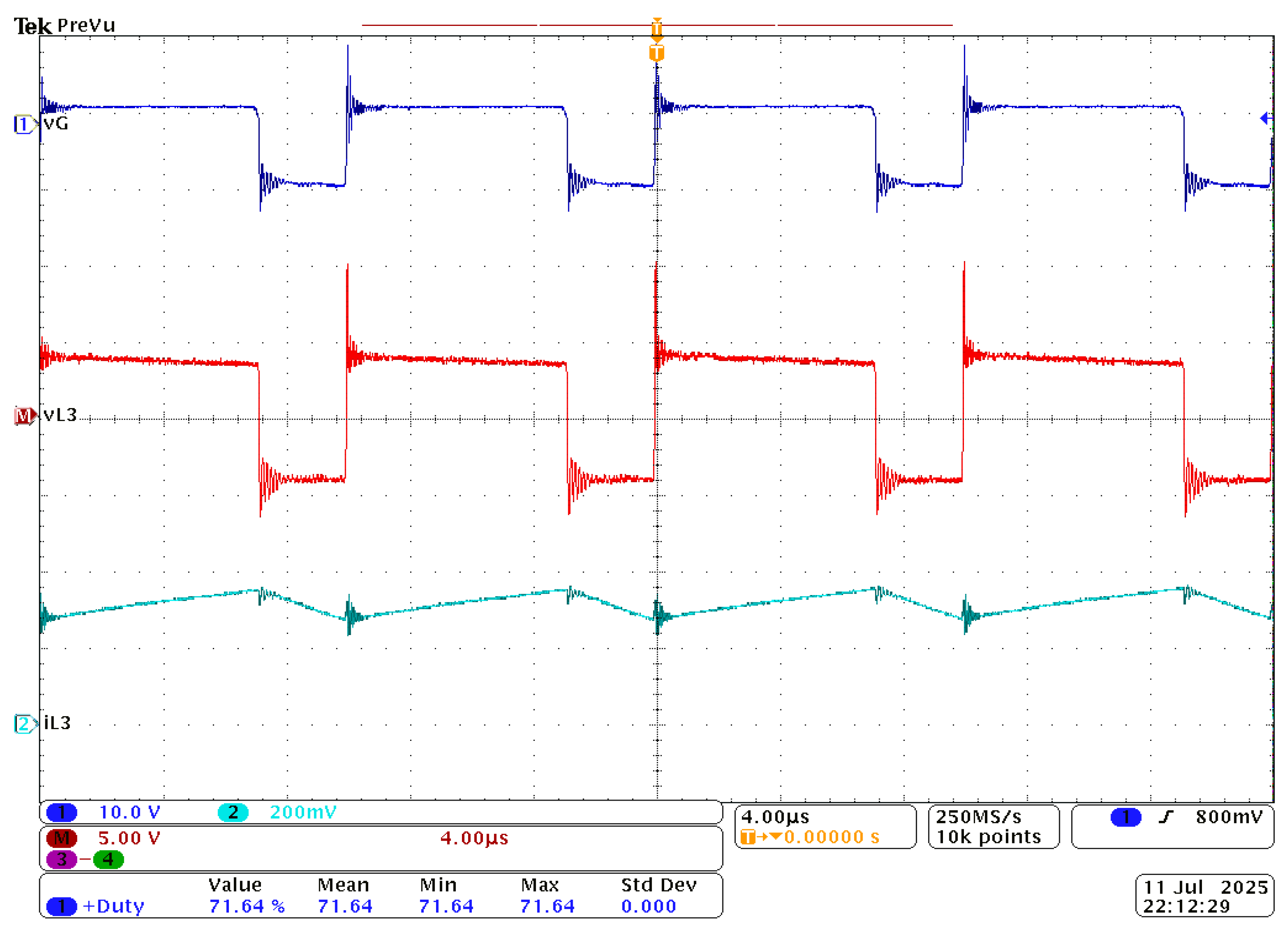
Experimental waveforms: vG—transistor gate voltage against supply ground (reference signal, acquired with attenuation of 10, represented with dark blue), vL3—voltage corresponding to inductor L3 (red), iL3—current through inductor L3 (light blue).
Figure 32.
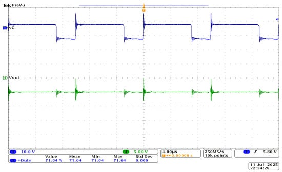
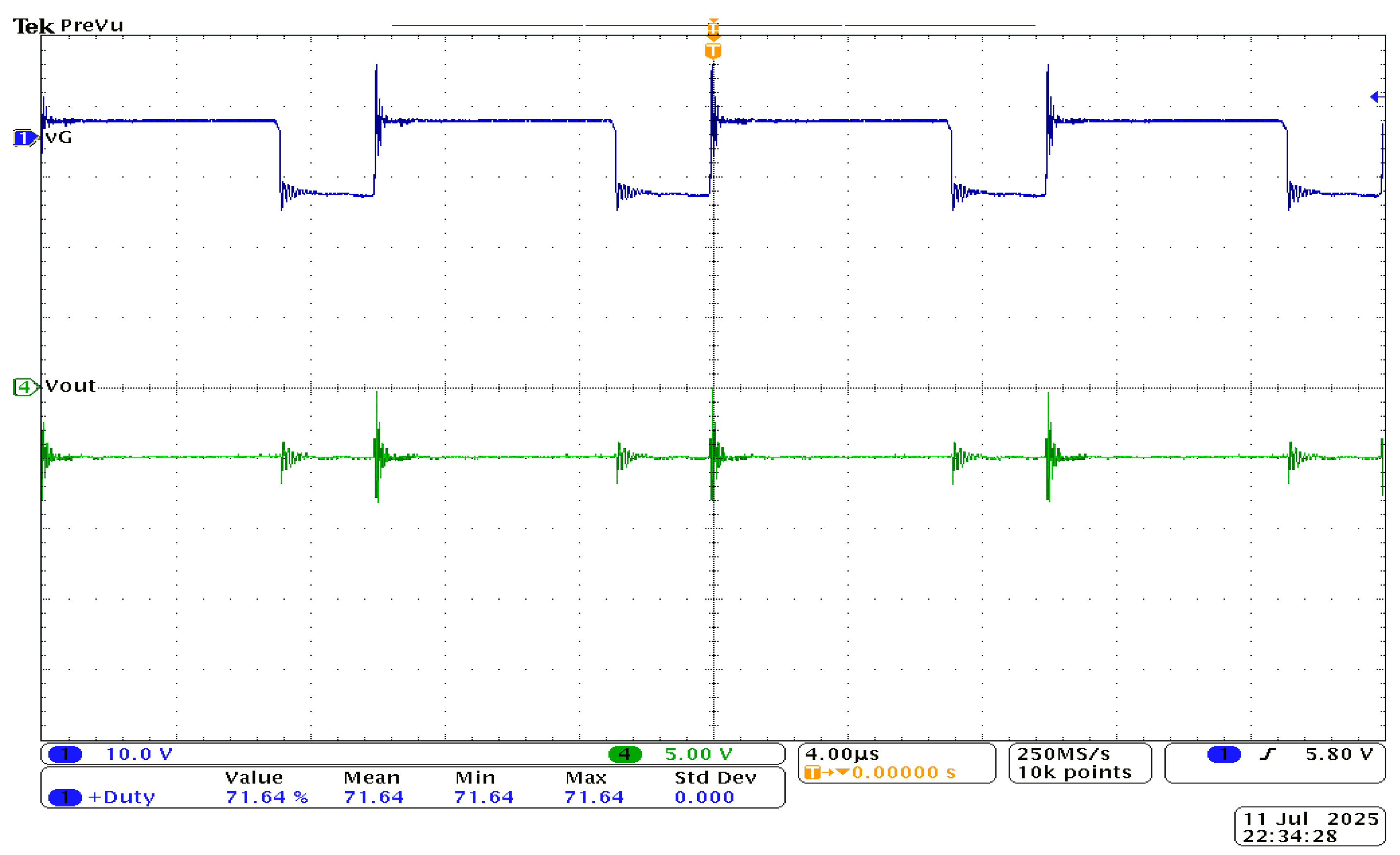
Experimental waveforms: vG—transistor gate voltage against supply ground (reference signal, acquired with attenuation of 10, represented with dark blue), Vout—output voltage (acquired with attenuation of 10, green).
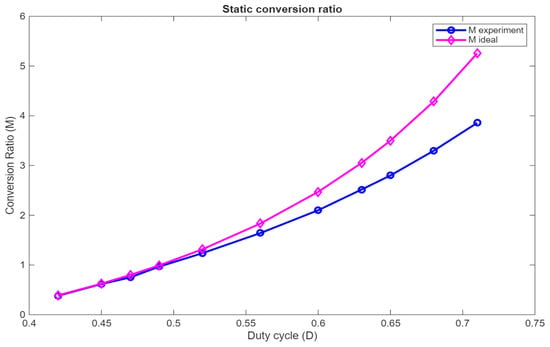
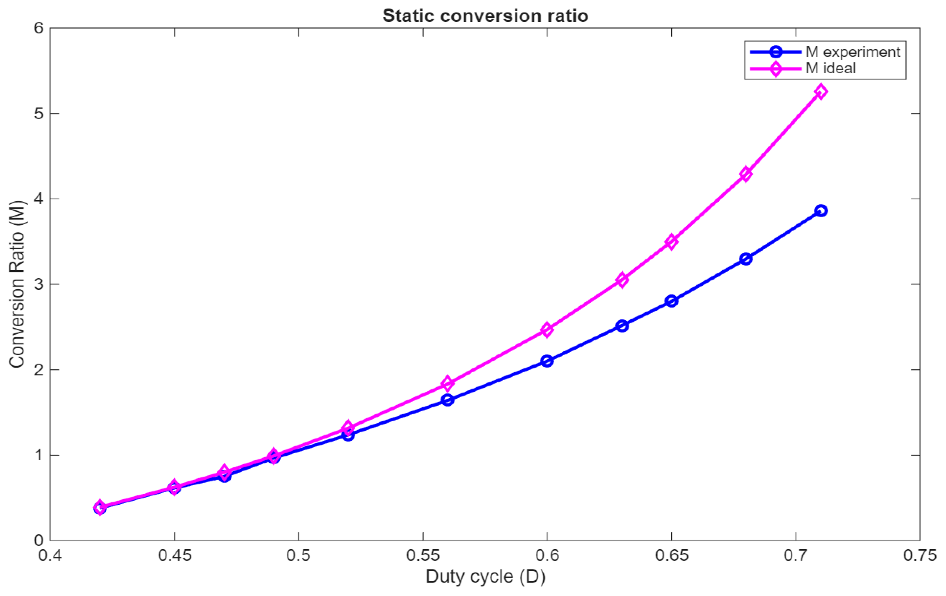
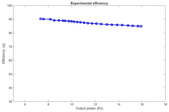
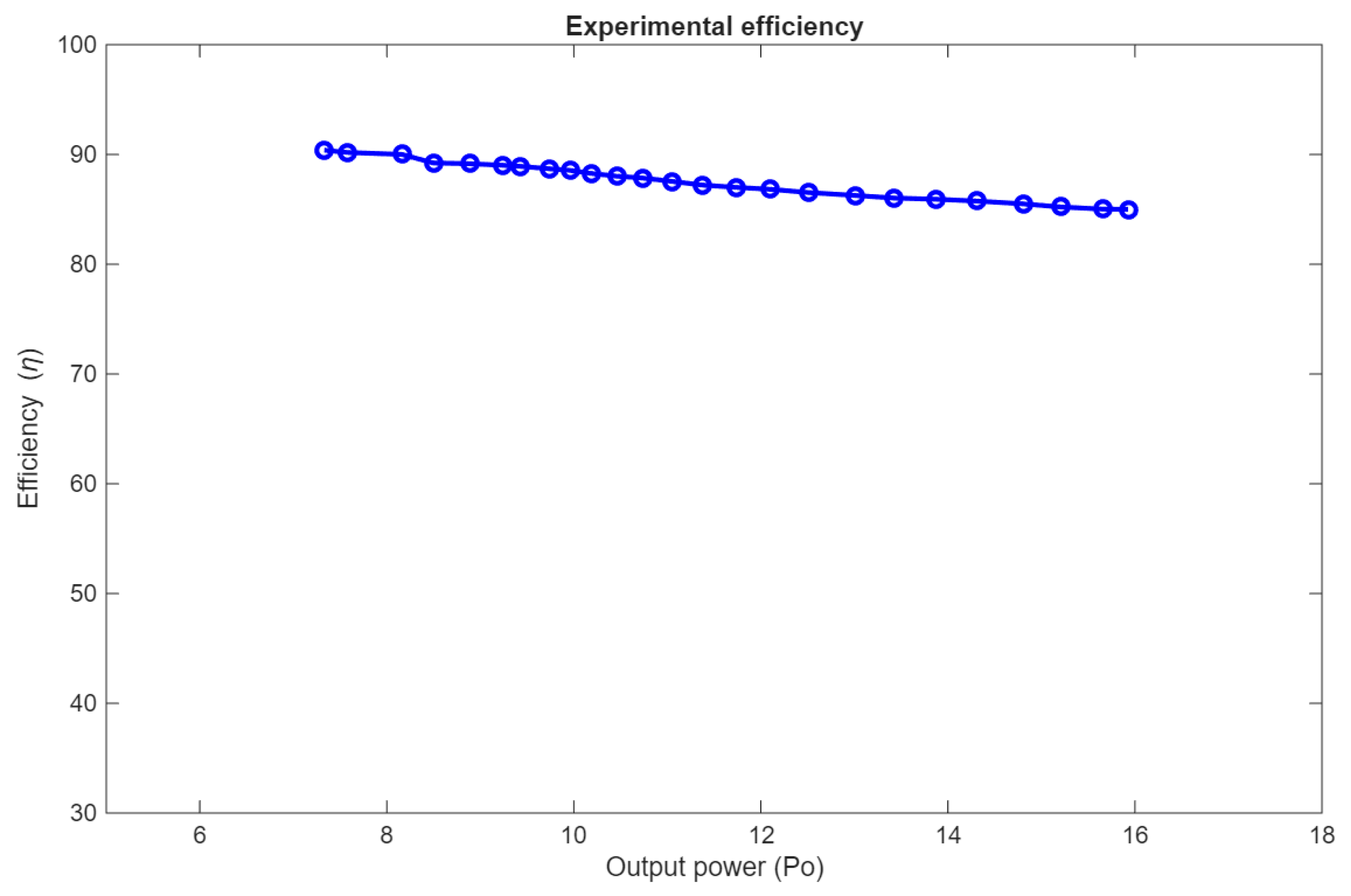
Based on the practical measurements, a comparison between the ideal static conversion ratio of the proposed converter and the one obtained from the experimental part has been performed. Figure 33 reveals that the experimental characteristic in the buck region almost overlapped the ideal one, while in the boost region, as expected, the experimental conversion ratio is below the ideal characteristic. Experimental efficiency against the output power is depicted in Figure 34. Reasonable values around 90% are obtained, with a typical drop at high-duty cycles mainly due to the transistor on-resistance.
Figure 33.
Static conversion ratio—ideal (pink) and from the experiment (blue).
Figure 34.
Experimental efficiency for the proposed converter.
4. Discussion
The performance of the proposed buck–boost converter, with coupled inductors, was evaluated through simulation and experiment, considering both open-loop and closed-loop operation. The proposed converter achieves a high step-up conversion ratio while maintaining stable dynamic behavior. Taking into account the conduction losses, the analysis shows that the converter still provides a high step-up static conversion ratio, and the state-space model is a realistic representation of the practical operation.
Even if the converter is a fourth-order system, the classical control design techniques can be used, without compromising stability. A type III error amplifier was designed using the classical pole-zero placement method, and the simulation results demonstrated that the proposed control strategy is a good choice, with the system being stable and predictable even when changes in the input voltage or load resistance appear.
5. Conclusions
This paper presented an extensive investigation of a fourth-order DC–DC converter, employing coupled inductors, focusing on its analysis when conduction losses and ESR for the output capacitor are taken into account. Starting from steady state and small-signal analysis, the control-to-output transfer function was derived using a matrix-based state-space approach that considers the mentioned losses. The results from MATLAB and PLECS validate the theoretical study. Using the classical pole-zero placement method, a type III error amplifier was successfully designed, and the closed-loop response shows that the system is stable, with a good phase margin and good response to changes in the input voltage and output load. The applications where this converter can be used include energy harvesting systems, power conditioning for sensor nodes, IoT, and, in general, all the applications requiring conversions with a large step-up.
Author Contributions
Conceptualization, D.-A.B., I.-M.P.-C., D.L. and G.-C.Z.; methodology, D.-A.B., I.-M.P.-C. and D.L.; software, D.-A.B.; validation, D.-A.B. and I.-M.P.-C.; formal analysis, D.-A.B. and D.L.; investigation, D.-A.B. and I.-M.P.-C.; data curation, D.-A.B., I.-M.P.-C. and D.L.; writing—original draft preparation, D.-A.B. and I.-M.P.-C.; writing—review and editing, D.-A.B., I.-M.P.-C. and D.L.; supervision, D.L. All authors have read and agreed to the published version of the manuscript.
Funding
This research received no external funding.
Data Availability Statement
Data are contained within the article.
Conflicts of Interest
The authors declare no conflicts of interest.
References
- Andrade, P.; Alcaso, A.N.; Bento, F.; Cardoso, A.J.M. Buck-Boost DC-DC Converters for Fuel Cell Applications in DC Microgrids—State-of-the-Art. Electronics 2022, 11, 3941. [Google Scholar] [CrossRef] [Scilit]
- Erickson, R.W.; Maksimovic, D. Fundamentals of Power Electronics, 3rd ed; Springer: Berlin, Germany, 2020. [Google Scholar]
- Yi, F.; Wang, F. Review of Voltage-Bucking/Boosting Techniques, Topologies, and Applications. Energies 2023, 16, 842. [Google Scholar] [CrossRef] [Scilit]
- Kumar, M.; Yadav, V.K.; Verma, A.K. Switched Capacitor Based High Gain Boost Converter for Renewable Energy Application. IEEE J. Emerg. Sel. Top. Ind. Electron. 2023, 4, 818–826. [Google Scholar] [CrossRef] [Scilit]
- Axelrod, B.; Berkovich, Y.; Ioinovici, A. Switched-Capacitor/Switched-Inductor Structures for Getting Transformerless Hybrid DC–DC PWM Converters. IEEE Trans. Circ. Syst. 2008, 55, 687–696. [Google Scholar] [CrossRef] [Scilit]
- Axelrod, B.; Berkovich, Y.; Ioinovici, A. Switched-capacitor (SC)/switched inductor (SL) structures for getting hybrid step-down Cuk/Sepic/Zeta converters. In Proceedings of the 2006 IEEE International Symposium on Circuits and Systems (ISCAS‘06), Kos, Greece, 21–24 May 2006. [Google Scholar] [CrossRef] [Scilit]
- Axelrod, B.; Berkovich, Y.; Ioinovici, A. Transformerless dc–dc Converters with a Very High dc Line-to-Load Voltage Ratio. In Proceedings of the 2003 International Symposium on Circuits and Systems (ISCAS‘03), Bangkok, Thailand, 25–28 May 2003. [Google Scholar] [CrossRef] [Scilit]
- Axelrod, B.; Berkovich, Y.; Ioinovici, A. Hybrid switched-capacitor-Cuk/Zeta/Sepic converters in step-up mode. In Proceedings of the IEEE International Symposium on Circuits and Systems (ISCAS), Kobe, Japan, 23–26 May 2005. [Google Scholar] [CrossRef] [Scilit]
- Hamood-Ur-Rehman; Ahmed, N.; Sher, H.A.; Al-Durra, A.; Hasanien, H.M. Comprehensive analysis and design of a switched-inductor type low inductance-requirement DC-DC buck-boost converter for low power applications. IET Power Electron. 2023, 16, 1239–1254. [Google Scholar] [CrossRef] [Scilit]
- Alizadeh, D.; Babaei, E.; Mousavi, S.M.J. High conversion ratio buck–boost DC–DC converter based on coupled inductor. IET Power Electron. 2023, 16, 645–658. [Google Scholar] [CrossRef] [Scilit]
- Zhang, N.; Zhang, G.; See, K.W.; Zhang, B. A Single-Switch Quadratic Buck–Boost Converter with Continuous Input Port Current and Continuous Output Port Current. IEEE Trans. Power Electron. 2018, 33, 4157–4166. [Google Scholar] [CrossRef] [Scilit]
- Gholizadeh, H.; Sarikhani, A.; Hamzeh, M. A Transformerless Quadratic Buck-Boost Converter Suitable for Renewable Applications. In Proceedings of the 10th International Power Electronics, Drive Systems and Technologies Conference (PEDSTC), Shiraz, Iran, 12–14 February 2019; pp. 470–474. [Google Scholar] [CrossRef] [Scilit]
- Gholizadeh, H.; Gorji, S.A.; Sera, D. A Quadratic Buck-Boost Converter with Continuous Input and Output Currents. IEEE Access 2023, 11, 22376–22393. [Google Scholar] [CrossRef] [Scilit]
- Bagewadi, M.D.; Dambhare, S.S. A Buck-Boost topology based hybrid converter for standalone nanogrid applications. In Proceedings of the IEEE Second International Conference on DC Microgrids (ICDCM), Nuremburg, Germany, 27–29 June 2017; pp. 502–506. [Google Scholar]
- Flores-Bahamonde, F.; Rivera, M.; Baier, C.; Calvente, J.; Giral, R.; Restrepo, C. DC transformer based on the versatile DC-DC noninverting buck-boost converter for fuel cell emulation. In Proceedings of the IEEE Southern Power Electronics Conference (SPEC), Puerto Varas, Chile, 4–7 December 2017; pp. 1–6. [Google Scholar]
- Okati, M.; Osmani-Bojd, M.; Samimi, S. A New Non-isolated Buck-Boost DC/DC Converter Based on Cuk Topology with Single Switch for Renewable Energy Application. Signal Process. Renew. Energy 2024, 8, 1–20. [Google Scholar] [CrossRef]
- Lazar, B.; Lascu, D. Fourth-Order Buck-Boost Converters Exhibiting Minimum Phase by Reverse Inductor Coupling. In Proceedings of the 2020 International Symposium on Electronics and Telecommunications (ISETC), Timisoara, Romania, 5–6 November 2020; pp. 1–4. [Google Scholar] [CrossRef] [Scilit]
- Zakaria, A.; Marei, M.I.; Mashaly, H.M. A Hybrid Interleaved DC-DC Converter Based on Buck-Boost topologies for Medium Voltage Applications. e-Prime-Adv. Electr. Eng. Electron. Energy 2023, 6, 100301. [Google Scholar] [CrossRef] [Scilit]
- Kumar, B.H.; Parimalasundar, E.; Muga, T.; Vari, K.K.R.R.; Gari, S.S.S.; Potlapadu, R.K.R. A Review of Non-Isolated DC-DC Converter Topologies. In Proceedings of the 2024 International Conference on Recent Innovation in Smart and Sustainable Technology (ICRISST), Bengaluru, India, 15–16 March 2024; pp. 1–6. [Google Scholar] [CrossRef] [Scilit]
- Sayed, S.S.; Massoud, A.M. Review on State-of-the-Art Unidirectional Non-Isolated Power Factor Correction Converters for Short-/Long-Distance Electric Vehicles. IEEE Access 2022, 10, 11308–11340. [Google Scholar] [CrossRef] [Scilit]
- Mishra, S.C.; Nanda, L.; Misra, B. Review and Comparison of DC-DC Buck Boost and Boost Converter Topologies for Fuel Cell Integration in Electric Vehicles and Microgrids. In Proceedings of the 2025 IEEE 1st International Conference on Smart and Sustainable Developments in Electrical Engineering (SSDEE), Dhanbad, India, 28 February–2 March 2025; pp. 1–7. [Google Scholar] [CrossRef] [Scilit]
- Khuntia, M.R.; Veerachary, M. Extended Boosting Range-Based-Non-Isolated Buck-Boost Converters with Continuous Input Current and Common Grounded Structure. IEEE J. Emerg. Sel. Top. Ind. Electron. 2024, 5, 813–826. [Google Scholar] [CrossRef] [Scilit]
- Miao, S.; Gao, J. A Family of Inverting Buck-Boost Converters with Extended Conversion Ratios. IEEE Access 2019, 7, 130197–130205. [Google Scholar] [CrossRef] [Scilit]
- Afshari, H.; Husev, O.; Vinnikov, D. A Novel Isolated Buck-Boost dc-dc Converter with Wide Range of Voltage Regulations. In Proceedings of the 2023 IEEE 17th International Conference on Compatibility, Power Electronics and Power Engineering (CPE-POWERENG), Tallinn, Estonia, 14–16 June 2023; pp. 1–6. [Google Scholar] [CrossRef] [Scilit]
- Pires, V.F.; Foito, D.; Cordeiro, A.; Pereira, P.; Roncero-Clemente, C.; Martins, J. Single-Switch Non-Isolated Buck-Boost DC-DC Converter with Wide Voltage Conversion Ratio. In Proceedings of the IECON 2024-50th Annual Conference of the IEEE Industrial Electronics Society, Chicago, IL, USA, 3–6 November 2024; pp. 1–6. [Google Scholar] [CrossRef] [Scilit]
- Mandal, S.; Prabhakaran, P. A Novel High Gain Unidirectional Buck-Boost DC-DC Converter with Active Switched-Inductor Configuration. In Proceedings of the 2023 IEEE International Conference on Power Electronics, Smart Grid, and Renewable Energy (PESGRE), Trivandrum, India, 17–20 December 2023; pp. 1–6. [Google Scholar] [CrossRef] [Scilit]
- Kamalinejad, K.; Iman-Eini, H.; Aleyasin, S.H.; Ghadi, M.A. A Novel Nonisolated Buck–Boost DC–DC Converter with Low Voltage Stress on Components. IEEE J. Emerg. Sel. Top. Ind. Electron. 2023, 4, 492–501. [Google Scholar] [CrossRef] [Scilit]
- ShyamSanjai, S.; Sivanathan, T.; Venmathi, M. Analysis and Implementation of Isolated Twin Buck-Boost Converter for EV Applications. In Proceedings of the 2024 International Conference on Distributed Computing and Optimization Techniques (ICDCOT), Bengaluru, India, 15–16 March 2024; pp. 1–5. [Google Scholar] [CrossRef] [Scilit]
- Kalaiarasi, A.R.; Dharani, M.; Josphin, A.J.; Rithubarnika, A. A Review on Error Reduction in a Closed-Loop Buck-Boost Converter Through the Implementation of Different Controllers. In Proceedings of the 2024 International Conference on IoT Based Control Networks and Intelligent Systems (ICICNIS), Bengaluru, India, 17–18 December 2024; pp. 677–683. [Google Scholar] [CrossRef] [Scilit]
- Lu, Y.; Wu, H.; Sun, K.; Xing, Y. A Family of Isolated Buck-Boost Converters Based on Semiactive Rectifiers for High-Output Voltage Applications. IEEE Trans. Power Electron. 2016, 31, 6327–6340. [Google Scholar] [CrossRef] [Scilit]
- Banerjee, A.; Praween, G.; Gupta, O.H.; Kumar, S.; Bhushan, R. Design, Simulation & Operation of Buck-Boost Converter for Renewable Energy Application. In Proceedings of the 10th IEEE Uttar Pradesh Section International Conference on Electrical, Electronics and Computer Engineering (UPCON), Gautam Buddha Nagar, India, 1–3 December 2023; pp. 996–1000. [Google Scholar] [CrossRef] [Scilit]
- Zhang, F.; Xie, Y.; Hu, Y.; Chen, G.; Wang, X. A Hybrid Boost–Flyback/Flyback Microinverter for Photovoltaic Applications. IEEE Trans. Ind. Electron. 2020, 67, 308–318. [Google Scholar] [CrossRef] [Scilit]
- Delavaripour, H.; Dehkordi, B.M.; Zarchi, H.A.; Adib, E. Increasing Energy Capture from Partially Shaded PV String Using Differential Power Processing. IEEE Trans. Ind. Electron. 2019, 66, 7672–7682. [Google Scholar] [CrossRef] [Scilit]
- Vinusha, B.; Kalpana, R.; Kishan, D. A Non-Isolated Buck-Boost DC-DC Converter for On-Board Electric Vehicle Powertrain. In Proceedings of the 2023 IEEE International Conference on Power Electronics, Smart Grid, and Renewable Energy (PESGRE), Trivandrum, India, 17–20 December 2023; pp. 1–6. [Google Scholar] [CrossRef] [Scilit]
- Bhanu, P.; Deekshitha, K.; Jayanth, V.; Sandeep, V. Comparative Performance Analysis of Buck-Boost, SEPIC and Zeta Converters for Active Cell Balancing in EV Batteries. In Proceedings of the 2024 International Conference on Social and Sustainable Innovations in Technology and Engineering (SASI-ITE), Tadepalligudem, India, 23–25 February 2024; pp. 224–229. [Google Scholar]
- Zhang, R.; Wu, J.; Wang, R.; Yan, R.; Zhu, Y.; He, X. A Novel Battery Management System Architecture Based on an Isolated Power/Data Multiplexing Transmission Bus. IEEE Trans. Ind. Electron. 2019, 66, 5979–5991. [Google Scholar] [CrossRef] [Scilit]
- Kim, K.-D.; Lee, H.-M.; Hong, S.-W.; Cho, G.-H. A Noninverting Buck–Boost Converter with State-Based Current Control for Li-ion Battery Management in Mobile Applications. IEEE Trans. Ind. Electron. 2019, 66, 9623–9627. [Google Scholar] [CrossRef] [Scilit]
- Lica, S.; Pop-Calimanu, I.-M.; Lascu, D.; Popescu, S.; Tomoroga, M.; Ciresan, A. A New Hybrid Ćuk Converter. In Proceedings of the 2018 International Symposium on Electronics and Telecommunications (ISETC), Timisoara, Romania, 8–9 November 2018; pp. 1–4. [Google Scholar] [CrossRef] [Scilit]
- Hasanpour, S.; Baghramian, A.; Mojallali, H. Analysis and Modeling of a New Coupled-Inductor Buck–Boost DC–DC Converter for Renewable Energy Applications. IEEE Trans. Power Electron. 2020, 35, 8088–8101. [Google Scholar] [CrossRef] [Scilit]
- Cheng, X.-F.; Zhang, Y.; Yin, C. A Family of Coupled-Inductor-Based Soft-Switching DC–DC Converter with Double Synchronous Rectification. IEEE Trans. Ind. Electron. 2019, 66, 6936–6946. [Google Scholar] [CrossRef] [Scilit]
- Maheri, H.M.; Heris, P.C.; Saadatizadeh, Z.; Babaei, E.; Vinnikov, D. A New Coupled-Inductor-Based Buck/Boost DC/DC Converter with Soft Switching for DC Microgrid Applications. In Proceedings of the 2021 IEEE 15th International Conference on Compatibility, Power Electronics and Power Engineering (CPE-POWERENG), Florence, Italy, 14–16 July 2021; pp. 1–6. [Google Scholar] [CrossRef] [Scilit]
- Botila, D.-A.; Zaharia, G.-C.; Pop-Calimanu, I.-M. A Buck-Boost Converter with Coupled Inductors for High Voltage Boosting Performance. In Proceedings of the 2024 International Symposium on Electronics and Telecommunications (ISETC), Timisoara, Romania, 7–8 November 2024; pp. 1–5. [Google Scholar] [CrossRef] [Scilit]
- Mathworks, MATLAB User Manual. Available online: https://www.mathworks.com/help/matlab/index.html (accessed on 5 March 2025).
- Plexim, PLECS User Manual. Available online: https://www.plexim.com/download/documentation (accessed on 15 May 2025).
- Basso, C. Switch-Mode Power Supplies, Spice Simulations and Practical Designs, 2nd ed.; McGraw-Hill: New York, NY, USA, 2014. [Google Scholar]
- Ridley, R. Power Supply Design, Volume 1: Control; Ridley Engineering: Camarillo, CA, USA, 2011. [Google Scholar]
- Simulation Research, Caspoc User Manual. Available online: http://www.caspoc.com (accessed on 26 March 2025).

Disclaimer/Publisher’s Note: The statements, opinions and data contained in all publications are solely those of the individual author(s) and contributor(s) and not of MDPI and/or the editor(s). MDPI and/or the editor(s) disclaim responsibility for any injury to people or property resulting from any ideas, methods, instructions or products referred to in the content. |
© 2026 by the authors. Licensee MDPI, Basel, Switzerland. This article is an open access article distributed under the terms and conditions of the Creative Commons Attribution (CC BY) license.