


Abstract
NAND flash memory reliability is increasingly challenged by rising data density and frequent program/erase cycles. While Error Correction Codes (ECC) are standard, the simultaneous use of ECC-embedded NAND and ECC-capable host systems is generally avoided due to the risk of unpredictable behavior and file system corruption. Existing studies on the use of dual ECC primarily focus on switching between different ECC structures or adaptive decoding based on error rates and data characteristics. In contrast, this paper introduces a novel driver-level coordination framework that enables the concurrent and integrated operation of two independent ECC mechanisms. By managing the interaction within the Memory Technology Device (MTD) layer, our approach enables the simultaneous utilization of internal NAND ECC and host-side ECC—a combination traditionally considered incompatible. Our approach improves overall system reliability and relaxes product-matching restrictions. Although the solution introduces a minor latency penalty, it is highly effective for applications where data integrity is the primary concern. Experimental results demonstrate that our solution prevents data corruption and extends the lifetime of NAND flash memory.
1. Introduction
NAND flash memory has been widely used in systems like mobile devices, consumer electronics, automotive, and Solid State Drives (SSDs). With the increasing number of mobile systems, NAND flash memory is becoming more popular every year. This is because NAND flash memory has advantages such as large storage capacity, shock resistance, low power consumption, and low cost.
With the increasing amount of data that needs to be stored in the industry, manufacturers are doubling the density of NAND flash memory chips each year, and the technology of NAND flash memory keeps developing dramatically [1]. However, the dramatic development of increasing density brings more challenges for reliability. For instance, while Single-Level Cell (SLC) NAND flash memory typically guarantees up to 100,000 program/erase (P/E) cycles due to its single-bit storage per cell, Multi-Level Cell (MLC) NAND, which stores two bits per cell, experiences a significant reduction in endurance, with P/E cycles up to 10,000 [2].
Research presented in [3] analyzed field studies conducted by Facebook, Microsoft, and Google, uncovering the prevalence of several error types in NAND flash memory used in their servers, including retention, read disturb, write, and wear-out errors. The study further indicates that each company has developed unique approaches to address these issues in its solid-state drives. As an illustration, the research notes Google’s method of designating blocks as bad when uncorrectable errors or erase failures occur. A key finding of the study is that uncorrectable errors represent a major challenge in real-world deployments, with more than 90% of drives experiencing them.
Historical incidents, such as the 2015 data loss bugs in Apple [4] and Samsung SSDs [5] and the 2009 data corruption issues in Intel drives [6], serve as stark reminders that data reliability is not merely a desirable feature but an absolute necessity in modern storage systems. The potential consequences of data unreliability extend far beyond mere inconvenience, impacting businesses, organizations, and individuals alike. Data loss can lead to significant financial losses, disruption of critical operations, erosion of trust, and even legal repercussions. Therefore, data reliability must be considered as paramount, holding equal importance to data density and cost in the design and implementation of any storage solution.
NAND flash memory cells have a limited lifespan. Programming (writing) and erasing operations in NAND flash memory cells involve an electrical process. Repeated P/E cycles can cause electrons to become trapped in the oxide layer of NAND flash memory cells, leading to unwanted data corruption, known as endurance [7]. While manufacturers predict a lifetime for NAND flash memories, the exact point at which a specific cell fails is unpredictable. To address the issue of data corruption caused by endurance limitations, Error Correction Codes (ECC) are implemented for NAND flash memory systems [8].
ECC provides the capability to correct bit-flips (incorrect bits) in NAND flash memory, up to a specified threshold determined by the ECC algorithm in use. The raw bit error rate (RBER) is the ratio of bit errors to the total number of bits, while the uncorrectable bit error rate (UBER) represents the error rate after ECC is applied. In NAND flash memory datasheets, the UBER value typically ranges from to [9]. Additionally, ECC systems relay information about corrected bit errors to the host system. If the number of corrected bit errors exceeds a predefined threshold, the host marks the corresponding block as bad and excludes it from future use.
The ECC may be placed in NAND flash memories or the host units, which read/write data to NAND. For example, Toshiba (Kawasaki, Japan) has two types of NAND flash memory, SLC NAND and BENAND. While SLC NAND offers 24 nm technology with a density in a range of 1 Gbit to 128 Gbit by leaving ECC to the host side, BENAND offers the same technology with a maximum 8 Gbit density with embedded ECC to the chips inside as hardware. That means while the host side of SLC NAND memory flash must have ECC, the host side of the BENAND NAND memory flash does not require ECC [10]. Different manufacturers also offer NAND flash memory that either incorporates internal ECC functionality or lacks ECC capability, which requires ECC capability on the host side.
While error correction is fundamental for all NAND-based storage, the complexity of ECC architectures has evolved differently depending on the application—from raw NAND chips to sophisticated SSDs. Although single-ECC architectures have traditionally been the standard for raw NAND, dual-ECC configurations have recently emerged in academic and industrial literature, primarily to optimize latency and power consumption. Various implementations have been proposed to leverage this hierarchical structure: ref. [11] proposed a dual-ECC framework that strategically assigns strong error correction to rarely accessed data exhibiting high latency, while defaulting to a weaker, lower-latency code for standard workloads. Similarly, ref. [12] introduced a fast ECC engine for standard operations and triggers a stronger, higher-latency engine only when the bit error rate exceeds a specific threshold. In the same vein, ref. [13] described a dual-mode decoder designed to switch between low-power and high-power correction modes to optimize energy efficiency. However, these approaches primarily target SSD firmware ecosystems, operating as internal `black box’ mechanisms that manage wear leveling autonomously without exposing error statistics to the host OS.
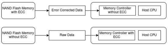
Regardless of the implementation strategy (internal, host-side, or hybrid), ECC must work during each read operation from NAND. That brings a latency penalty to read operations to the NAND flash memory, which boasts about read/write speed. In order to overcome this challenge, host-side manufacturers develop hardware interfaces (see Figure 1) to speed up the work of ECC and lower the latency caused by ECC for the CPU. Due to the advantages of this hardware unit, ECC calculations and the load of the CPU do not affect each other. For instance, NXP provides a hardware unit called the General-Purpose Media Interface (GPMI) [14] in its i.MX CPUs to accelerate ECC tasks. The GPMI applies error correction to the raw data read from the NAND and transfers it to the CPU in an error-corrected state, a feature that has made these processors a common choice for over ten years.
Figure 1.
Example SLC Benand Graph from Toshiba.
When selecting CPUs and NAND flash memory for their products, companies must carefully consider the existing ECC implementations. Due to the nature of these components, companies may need to use different controllers or storage solutions over the product’s lifetime. As previously mentioned, certain issues or bugs may not occur until the end of the NAND flash memory’s lifespan. It is well-known that operating NAND flash memory without any form of ECC will lead to data corruption within a short period of use.
While the standard approach is to implement ECC either on the host side or within the NAND flash itself, the Linux kernel architecture is natively designed to support only a single ECC source. Consequently, the simultaneous use of both is functionally decoupled; the host controller typically masks the internal error corrections of the device, creating a `visibility gap.’ Without coordination, this prevents the operating system from accessing the real-time error statistics required for effective wear leveling, often resulting in file system corruption or total system crashes. In this work, we provide a driver-level solution to bridge this architectural gap and effectively combine ECC-embedded NAND memories with ECC-capable host systems. We validated our approach using a setup featuring Toshiba BENAND NAND flash memory and an I.MX6 CPU. The results demonstrate the viability of the proposed solution; it enhances system reliability, albeit at the cost of a marginal latency penalty. Furthermore, this approach relaxes the constraints on product matching, facilitating greater flexibility in hardware procurement.
The subsequent sections of this paper are organized to guide the reader through our analysis. Section 2 lays the groundwork by explaining the architecture of NAND flash memory, various ECC implementation strategies, wear leveling algorithms, and bad block management procedures. Section 3 then delves into the specifics of memory management for NAND flash devices within the Linux environment. Section 4 details our proposed solution at the driver level. The experimental setup and the resulting findings are presented in Section 5. Lastly, Section 6 offers concluding remarks.
2. Background
2.1. NAND Flash Memory
The NAND flash memory is a basic floating gate and Metal-Oxide Semiconductor (MOS) transistor with a fixed threshold voltage. The electrical state of a NAND flash memory cannot be changed even with a power cut, which makes it a non-volatile memory. The process of tunneling electrons into the storage node is referred to as programming. Conversely, the removal of electrons from the storage node is referred to as erasing. When the P/E cycle is repeated excessively, some electrons become trapped in the oxide layer, which affects the voltage threshold of the memory cell. This side effect brings the disadvantage of the limited lifetime of the NAND flash memory. The lifetime of a NAND flash memory is characterized by its reliability, which is determined by two key properties. First, retention refers to the ability of a memory cell to maintain its programmed voltage level over time. Second, endurance refers to the maximum number of P/E cycles without significant electron loss during programming [7].
The first design of NAND flash memory [15], known as the SLC, stores one bit of data per memory cell. Following the development of MLC NAND flash memory, a single cell became capable of storing two bits of data by utilizing four distinct threshold voltage levels [16]. Building on this principle, triple-level cell (TLC) and quad-level cell (QLC) designs were developed. However, while increasing the number of bits stored per cell enhances storage density, it also reduces the reliability of the flash memory due to the narrower threshold voltage ranges required for distinguishing between multiple states. For example, narrower voltage windows increase the likelihood of read errors, as small variations in voltage can lead to misinterpretation of the stored data. This trade-off between density and reliability has become a critical consideration in the design of modern NAND flash memory technologies.
Another critical aspect of NAND flash memory design is its layered structure. Moore’s Law, which predicts the doubling of transistor density approximately every two years, pushed planar (2D) NAND flash memory to its physical limits. As a result, the shrinking cell size led to increased interference and higher bit error rates. To address these challenges, the industry introduced 3D NAND flash memory, which stacks multiple layers vertically and significantly increases storage density [17].
NAND flash memory is organized hierarchically. Each NAND flash memory chip is divided into blocks, and each block is further subdivided into pages. The typical page sizes for NAND flash memory are 2 KB, 4 KB, and 8 KB. Each block generally consists of 128, 256, or 512 pages.
2.2. Error Correction
ECC play a critical role in ensuring data integrity and reliability during data transmission between NAND flash memory and the host controller. ECC is a mathematical algorithm used to ensure data integrity by detecting and correcting errors, which is essential in NAND flash memory due to the inherent bit error rates caused by factors such as cell wear and P/E cycling. The calculated vectors, known as codewords, consist of a sector of user data combined with parity bits. According to the ECC design, a codeword will fall outside the defined code space if the number of errors exceeds a predefined threshold. The ECC is responsible for mapping the erroneous word back to the closest valid codeword. During a programming operation, the data is divided into 1-kB or 2-kB chunks. For each chunk, the ECC calculates the user data and its corresponding parity data, forming a codeword for each chunk. When the data are read back from the NAND flash memory, the ECC uses the parity data to detect and correct any bit errors. Common ECC algorithms, such as Bose-Chaudhuri-Hocquenghem (BCH) and Low-Density Parity Check (LDPC) codes, offer varying levels of error correction capability, typically correcting up to several bits per codeword. When implemented in hardware, the ECC uses an encoder circuit to generate codewords during programming and a decoder circuit to detect and correct errors during reading [18].
Most ECC engines are based on BCH [19] codes, a class of cyclic error-correcting codes known for their ability to detect and correct multiple bit errors. The codeword structure and error correction capability of the BCH codes are predefined, and the number of correctable bits directly influences the design. For example, a BCH code capable of correcting 4 bits per codeword requires 14 parity bits, while a code correcting 8 bits requires 28 parity bits. However, a higher correctable bit count requires additional parity bits in the codeword and more complex decoding logic in hardware, which can increase latency and power consumption, thereby negatively impacting read performance. This creates a critical trade-off between data reliability and system performance in NAND flash memory applications.
RBER and UBER are key metrics that characterize the ECC, demonstrating its effectiveness in ensuring data reliability. RBER (1), calculated as the ratio of bit errors to the total number of bits read, represents the error rate before ECC correction. In contrast, UBER (3), which reflects the ratio of uncorrectable errors to the total number of bits read, indicates the error rate that remains uncorrectable because the number of errors exceeds the ECC’s correction capability, meaning a codeword failure has occurred. The failure probability of a codeword is mathematically expressed in Equation (2), a formulation adopted from the work presented in [20]. In Equation (2), N is the number of codeword bits, E is the correctable bit count, and i is the error count.
UBER is a standardized metric for evaluating flash memory lifetime, as it directly reflects the point at which the memory becomes unreliable due to uncorrectable errors. This metric is critical for determining the endurance and reliability of NAND flash memory, which guides design and usage decisions [21].
In a NAND flash memory block, if the raw bit error count is above the correctable bits count by the ECC, uncorrectable errors occur. Experiments in [21] demonstrate the relationship between RBER and UBER for different correctable bit counts by the ECC engine. Table 1 summarizes the result of the experiment. As shown in the table, increasing the correctable bit count from 2 to 8 allows the same UBER value to be achieved at an RBER value times higher.
Table 1.
Relation between UBER and RBER for different number of correctable bits counts. A more detailed graph is presented in [21].
Recent advancements in NAND flash reliability have largely focused on internal algorithmic improvements. For instance, bilayer LDPC codes combined with perturbed decoding have been proposed to significantly extend MLC NAND lifetime [22]. Similarly, machine learning techniques have been increasingly applied to internal SSD optimization, as surveyed in [23], to predict wear patterns and optimize garbage collection strategies. On the architectural side, host-to-FTL pipelines have been explored to alleviate bandwidth bottlenecks in high-performance arrays [24].
However, these state-of-the-art solutions predominantly operate within the closed ecosystem of the SSD firmware or require specialized controller logic. They function under the assumption that the error correction process is transparent to the host. In contrast, in embedded systems utilizing Raw NAND with generic Linux drivers, a structural “visibility gap” emerges. Even if advanced ECC algorithms are present on-die, their correction status remains hidden from the Operating System’s wear-leveling subsystem. Unlike the mentioned algorithmic studies, this work addresses the system-level driver integration required to bridge this gap, ensuring that the OS is aware of the physical degradation handled by the hardware.
2.3. Wear Leveling and Bad Block Management
NAND flash memory cells have a finite number of P/E cycles, typically ranging from 10,000 to 1 billion, depending on the technology and architecture. Although ECC protects data integrity within individual blocks, more sophisticated management techniques are crucial for maximizing the memory’s overall lifespan. In systems utilizing NAND flash memory, two primary challenges limit the maximization of lifespan. First, certain blocks may experience significantly more write operations than others, leading to uneven wear distribution. Second, since an entire page must be erased before it can be reprogrammed, modifying data smaller than the page size necessitates reading, erasing, and rewriting the entire page. This results in excessive data transfer for relatively minor updates, known as write amplification. Furthermore, in the event of a power loss during the operation, the entire page of data may be lost, posing a significant risk to data reliability. The techniques designed to address these challenges are collectively referred to as wear-leveling [20].
Wear-leveling is a technique that redistributes data across NAND flash memory to ensure uniform wear across all memory blocks. To achieve this objective, wear-leveling employs a block-mapping technique that decouples the logical addresses used by the host system from the physical addresses utilized by the flash memory. While the host system operates with virtual block numbers, the flash memory manages data using physical addresses. Wear-leveling maps the same virtual block number to different physical addresses whenever data is updated, ensuring that new data is written to a new physical location. As a result, data is redistributed across the flash memory without requiring any changes or awareness from the host system [25].
Additionally, since modified data is written to a new physical page without erasing the old data, this approach provides the ability to prevent data loss caused by a power failure during programming operations. Once the update is successfully completed, the old physical page is marked as obsolete, and the garbage collection mechanism subsequently erases the data stored in that location.
As we mentioned earlier, a NAND Flash memory cell completes its lifetime after a certain amount of the P/E cycle, leading to faults in the block, a group of cells. Bad block management identifies these faulty blocks and marks them as invalid, ensuring that they are excluded from future write and read operations [26]. This process is critical for maintaining data integrity and preventing system failures. If the number of errors exceeds the correction capability, the block is flagged as potentially bad. Similarly, if a block consistently fails to program or erase, it is marked as defective.
To further enhance reliability, the file system plays an active role in identifying potential bad blocks. When errors in a specific region exceed a predefined threshold, the file system flags that area as a potential bad block. It then performs a series of tests to confirm whether the block is truly defective. These tests may include repeated read/write operations and error rate analysis. By proactively identifying and isolating bad blocks in this manner, the file system ensures that data is safely relocated to a healthy block before the defective block is marked as bad [27]. This approach minimizes the risk of data loss and maintains the overall integrity of the storage system.
3. Linux NAND Flash Memory Management
This section examines the underlying architecture of the Linux storage stack and the specific requirements for implementing our driver-level solution. While our analysis uses the Toshiba BENAND and i.MX6 GPMI controller as representative hardware, the approach is generalized for any system combining built-in ECC NAND flash memory with an ECC-capable host. By detailing the interactions between the MTD, UBI, and UBIFS layers, we provide the necessary context to understand how our solution resolves the structural incompatibilities of dual-ECC systems.
3.1. Linux Kernel Layers
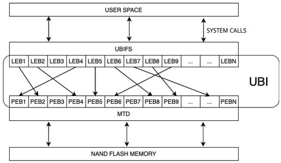
The Linux storage stack incorporates three layers between the NAND flash memory and user space. Figure 2 illustrates this layered architecture and the interactions between its components. The Memory Technology Devices (MTD) layer provides an abstraction of the raw flash memory. Above the MTD layer, the Unsorted Block Images (UBI) layer handles essential functions, including block mapping, wear-leveling, and bad block management. Finally, the UBI File System (UBIFS), a flash-optimized file system, operates on top of UBI volumes.
Figure 2.
Linux NAND Flash Memory Management Layers.
The MTD layer is the first layer, which interacts directly with the NAND flash memory device [28]. The layer provides a hardware-independent interface for managing raw flash devices and MTD character devices (/dev/mtd0, /dev/mtd1), which enable input/output operations for accessing the raw data stored in NAND flash memory. If the host supports ECC functionality, the raw data is processed by the ECC driver to detect and correct potential errors.
3.1.1. UBI Layer
The layer between UBIFS and MTD is UBI, a volume management system designed for raw flash memory devices [29]. UBI is designed according to wear-leveling rules, and it distributes I/O load to increase lifespan by dynamically mapping physical erase blocks (PEB) and logical erase blocks (LEB) to relocate data from more worn-out blocks to less worn-out blocks. UBI also handles bad blocks by replacing newly discovered bad blocks with the reserved good blocks, ensuring data integrity and preventing I/O errors. Another capability of the UBI volume is scrubbing, moving data from PEBs with bit-flip errors to other PEBs to prevent data corruption. Bit-flip errors may occur during read and write operations. The ECC corrects those bit-flips, but over time, the accumulation of the bit-flips can lead to data loss. All these processes are transparent to user space, which decreases the application programming load dramatically by abstracting complex tasks from users. As a result, the UBI layer effectively manages wear-leveling, bad blocks, and scrubbing, ensuring reliable and efficient operation of flash memory devices.
3.1.2. UBIFS Layer
UBIFS, a high-performance, flash-optimized file system, sits at the top of the stack, providing the interface for user-space interaction [30]. Its key advantages include efficient performance regardless of flash memory size, minimal memory footprint, and consistent I/O speeds. Furthermore, UBIFS offers robust power-cut tolerance through its journaling mechanism, enabling rapid recovery.
3.2. Linux Kernel ECC Drivers
In this section, the interaction between the Linux kernel and ECC mechanisms is examined, focusing on host-side ECC, the GPMI driver, and the ECC implementation in Toshiba BENAND NAND flash memory through their respective drivers.
The ECC functions are encapsulated within the nand_ecc_ctrl structure, which is included as the ecc member of the nand_chip structure. Both structures are defined in the /include/linux/mtd/rawnand.h file. The nand_ecc_ctrl structure holds key ECC parameters, such as the ECC engine type, error correction strength, and step size, along with function pointers for read and write operations provided by ECC drivers. The function pointers are assigned to the corresponding read and write functions from the ECC drivers. NAND flash memory drivers allocate the nand_chip structure by using kmalloc. Since the structure embeds an mtd structure, the MTD structure is reachable via nand_to_mtd() function. This design enables all of the structures to be universally utilized across MTD, NAND, and ECC drivers, ensuring a consistent interface for read, write, erase, and ECC operations. After a read operation, three distinct outcomes may occur: (1) correct data requiring no correction, (2) corrected data with a corrected bit-flip count, and (3) uncorrectable data. Corrected data influences the RBER, while uncorrectable data contributes to the UBER.
However, this architecture inherently assumes a single ECC source. The Linux MTD subsystem typically binds the ECC operations defined in nand_ecc_ctrl to a single driver instance, either the host controller or the on-die ECC mechanism. Consequently, the standard framework lacks native support for concurrent engines. When a host-side driver is initialized, it effectively shadows the internal status reporting of the memory device. This architectural exclusivity renders the simultaneous operation of dual ECC engines unnatural within the standard kernel framework, necessitating a custom coordination layer to expose the hidden internal statistics.
3.2.1. GPMI Driver
The GPMI driver [31], ECC hardware accelerator in NXP i.MX processors, retrieves raw data from NAND flash memory and process it. The driver is located in the drivers/mtd/nand/raw/gpmi-nand/ subdirectory.
The driver has gpmi_nand_data structure which includes the nand_chip structure as the nand member, in addition to other essential information. In the driver probe function, gpmi_nand_data is initialized using devm_kzalloc. After initializing, GPMI functions and parameters are assigned to the nand_ecc_ctrl structure within the gpmi_init_last() function. Elements of the nand_ecc_ctrl structure and the corresponding initialization values are given in Table 2. A final step in the initialization is to set the layout of the out-of-band area through mtd_set_ooblayout(mtd, &gpmi_ooblayout_ops) function.
Table 2.
Initialization values of the nand_ecc_ctrl structure for GPMI.
The ECC engine type is configured as NAND_ECC_ENGINE_TYPE_ON_HOST, indicating that the ECC operations are performed on the host side. The read functions utilize gpmi_count_bitflips() to return the bit-flip count. As previously mentioned, the function returns specific values to indicate the status of the data:
- 0x00 (STATUS_GOOD) signifies that no correction was required,
- 0xFE (STATUS_UNCORRECTABLE) indicates the presence of uncorrectable errors, and
- a numerical value representing the count of corrected bit-flips is returned if errors were successfully corrected.
The corrected bit-flip count is forwarded to the UBI volume for scrubbing and wear-leveling.
3.2.2. Toshiba BENAND Driver
Toshiba NAND driver [32] designed to read data from different Toshiba NAND flash memories, including BENAND. The driver is located in the /drivers/mtd/nand/raw/nand_toshiba.c file.
In the driver’s initialization function, the driver checks whether the chip ID matches with BENAND and the ECC engine type is ON-DIE. If these conditions are met, the driver configures the nand_ecc_ctrl structure with BENAND functions and parameters within the toshiba_nand_benand_init() function. The associated nand_ecc_ctrl structure and the initialization values can be found in Table 3.
Table 3.
Initialization values of the nand_ecc_ctrl structure for BENAND.
The read function returns with the function toshiba_nand_benand_eccstatus(), which sends the 0x7A (TOSHIBA_NAND_CMD_ECC_STATUS_READ) command to the NAND to read the ECC status. As is similar to GPMI, the read data’s ECC status is indicated through specific values returned by the function:
- 0x00 (STATUS GOOD) is returned when no correction is needed.
- 0x0F (STATUS UNCORRECTABLE) is used to signal the presence of uncorrectable errors.
- If errors are corrected, the function provides a numerical value indicating the number of fixed bit-flips.
If the status is uncorrectable, the UBER count is incremented, and the read operation is marked as failed. If there are corrected bit-flips, the UBI volume receives the corrected bit-flip count for scrubbing and wear-leveling purposes.
It is observed that, while the GPMI driver forces the ECC engine type to be set to ON-HOST, the BENAND driver ensures that the type is verified and configures the relative functions when the type is ON-DIE. Consequently, the GPMI functions remain in use despite the system’s support for ECC engines on both sides.
4. Methodology for Dual-ECC Coordination
As previously mentioned, when a memory cell containing valid data experiences uncorrectable errors, data loss occurs. To address this, the Linux kernel is designed to prevent the use of memory cells that are likely to develop uncorrectable errors by monitoring and counting correctable errors at the UBI layer, which are obtained from the MTD layer. However, the effectiveness of this preventive mechanism relies entirely on the visibility of error statistics.
In Section 3, we analyzed the interaction between NAND flash memory drivers and the MTD layer. As highlighted in Section 3.2, the Linux kernel architecture inherently assumes a single source of truth for error correction. Consequently, in a system equipped with both GPMI and BENAND ECC engines, the GPMI driver’s functions take priority, effectively `shadowing’ the BENAND driver. This results in the BENAND driver’s functions being ignored, and while the correctable bit count from the GPMI driver is reported, the statistics from the BENAND driver are disregarded, creating a blind spot that leads to unmanaged uncorrectable errors.
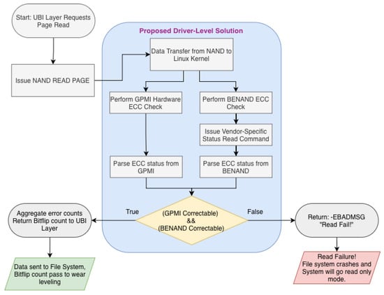
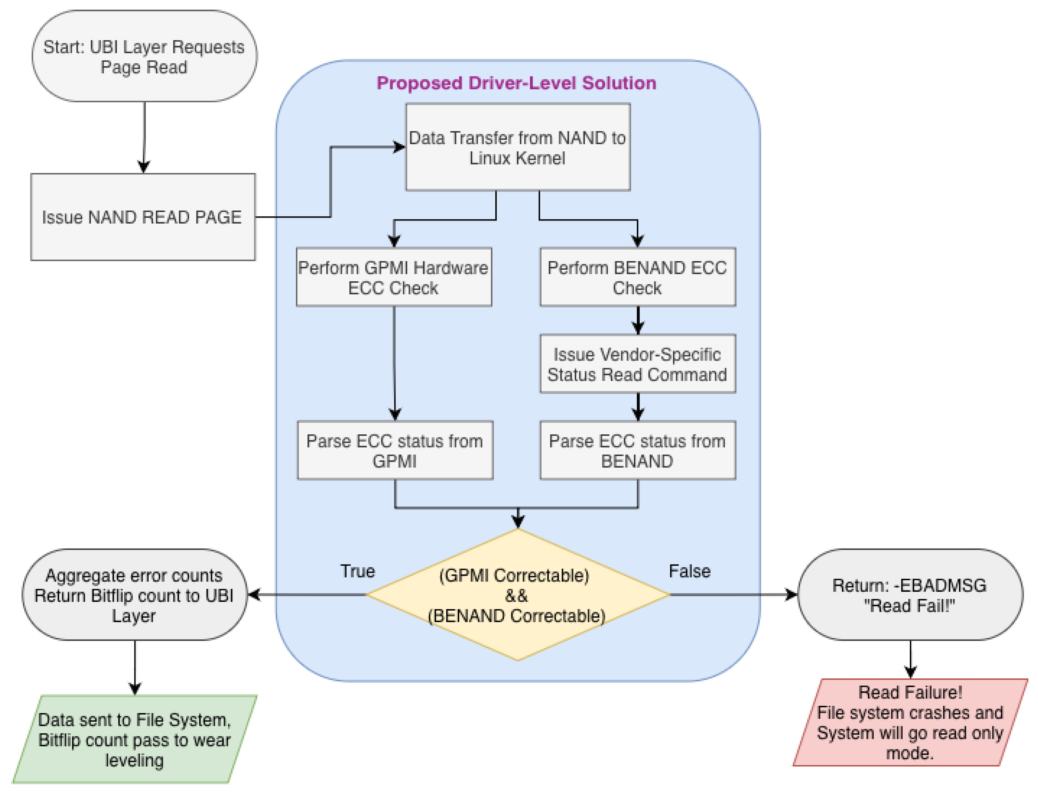
To resolve this conflict, the solution must be implemented at the same architectural layer where the wear-leveling decisions are made. Therefore, we propose sending an ECC status read command to the BENAND driver while using the GPMI driver’s functions. This approach allows us to retrieve ECC statuses from both engines, enabling the system to leverage the functionality of both ECC engines and enhance data reliability. The source code patch is shared on our GitHub repository [33]. While Figure 3 illustrates how our proposed solution is placed in the corresponding Linux Kernel layers. The process begins when the driver intercepts a standard read request. Instead of immediately returning, the driver injects a vendor-specific status command (e.g., 0x7A for Toshiba BENAND) to query the NAND ECC engine. The driver then retrieves the internal bit error count and aggregates it with the host controller’s report. This step resolves the visibility conflict by ensuring that the upper MTD layers receive the cumulative error count—reflecting both the host and device status—rather than an incomplete zero-error report.
Figure 3.
A general chart of proposed solution.
It is important to note that the proposed solution does not modify the wear-leveling algorithms of the UBI subsystem. Instead, it ensures compatibility with the existing Linux layers. By transparently exposing aggregated error statistics to the MTD layer, the standard UBI subsystem is enabled to accurately monitor block health and trigger the default scrubbing and torturing mechanism when necessary. Without this coordination, the standard wear-leveling mechanism would remain blind to error correction events in BENAND, leading to a failure in retiring compromised blocks in a timely manner.
5. Experimental Results
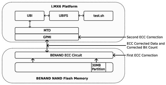
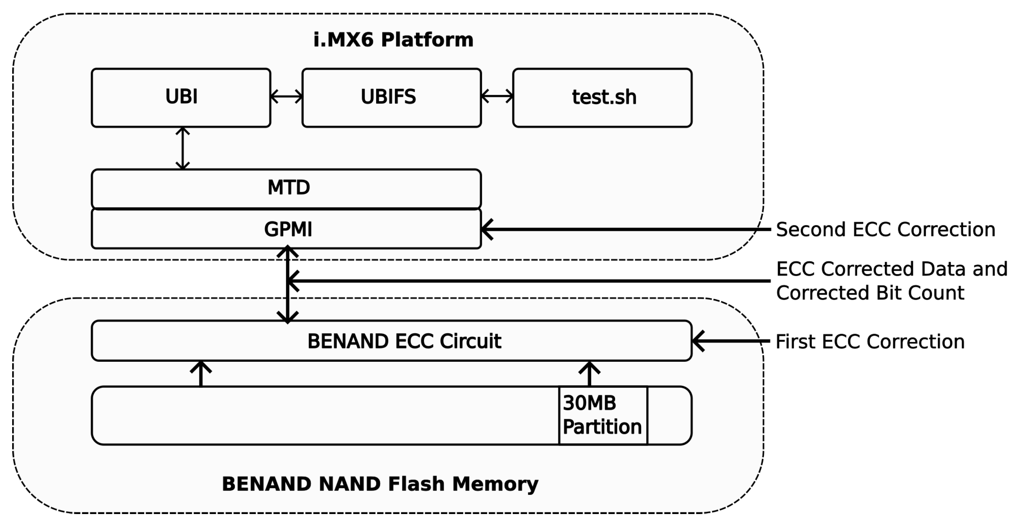
To evaluate the efficacy and reliability of the proposed driver-level solution, we established a dedicated test environment. While this validation utilizes Toshiba BENAND and the NXP i.MX6 CPU, the setup (see Figure 4) serves as a representative case study for generic systems combining on-die and host-side ECC engines. The test scripts and the result logs are shared on our GitHub repository [33].
Figure 4.
A general overview of test environment.
The experimental environment comprises six independent pairs of Toshiba BENAND flash memory and i.MX6 CPUs running Linux kernel version 5.4.0. To assess endurance, each system was subjected to continuous P/E cycles, ranging from 0 to 100,000 cycles.
A specific partitioning strategy was implemented to facilitate these endurance tests within a practical timeframe. Rather than utilizing the full capacity of the 1GB NAND chip—which would distribute wear across too many blocks and require years to reach end-of-life—we allocated a 5 MB active partition. This was achieved by defining a 30 MB area consisting of 120 Physical Erase Blocks (PEBs), each 256 KiB in size. Each block consists of 64 pages, each 4 KiB in size. Within this 120-PEB pool, 36 blocks are designated as available, while the remaining 84 blocks are reserved. This isolated configuration ensures that the 36 active blocks reach their maximum P/E cycle limits much faster, allowing for a comprehensive observation of bit-flip behavior and ECC coordination during the memory’s late-life stages.
In our tests, we repeatedly wrote, verified, and erased data on tests with existing drivers and with our proposed solution. The maximum P/E cycle is adjusted to 100,000. Results are presented in Table 4. As shown in the table, existing drivers cannot go beyond 16K P/E cycles. This is due to the fact that built-in ECC does not report the bit-flip count to the UBI layer. Thus, UBI can not trigger a bad block check. On the other hand, thanks to its dual ECC coordination, our proposed solution is capable of completing the whole test and successfully labeling bad blocks.
Table 4.
Comparison of the existing drivers with the proposed solution over 100,000 P/E cycles. Due to the visibility gap existing drivers leads to a file system crash around 15K P/E cycles. On the other hand use of the proposed system enables detection of bad blocks and system can complete 100,000 P/E cycles.
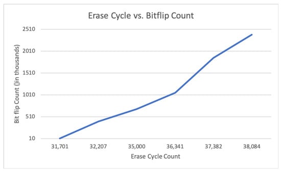
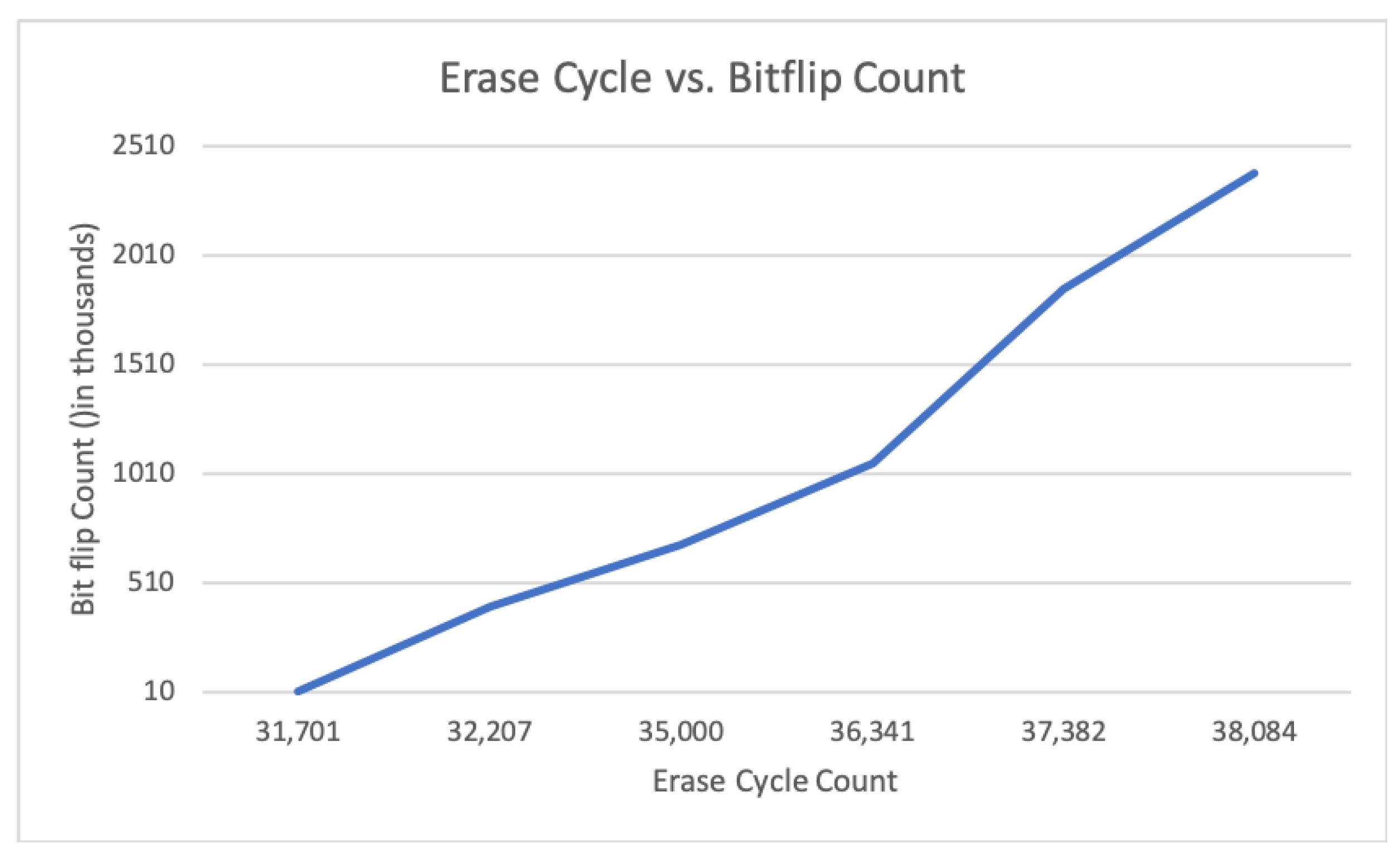
During our test, we also investigated the relationship between the erase cycle count and the bit-flip and observed that it is non-linear as shown in Figure 5. During the initial stages of the memory’s lifespan, bit-flips occur sporadically. However, after a specific threshold, the frequency of bit-flips increases aggressively.
Figure 5.
Relation between erase cycle count and bit-flip count till detection of first bad block.
This aggressive increment explains the sudden file system crashes observed in standard drivers. When the “visibility gap” exists, the system is unable to track these internal corrections. By the time the errors exceed the host’s correction threshold, the system has no warning, leading to the catastrophic failures shown in our results. By contrast, our solution monitors this aggressive curve, allowing for controlled bad-block marking even as error rates spike.
We also evaluated the overhead of our proposed system by conducting read/write tests for different data sizes. Table 5 shows the read/write speeds for different data block sizes, with a total test size of 100 MB. The observed 26.3% reduction in read throughput is a direct consequence of the 55 μs delay required to query the on-die ECC status register for every page read operation. While this penalty is measurable, its significance must be weighed against the operational requirements of the target system. In industrial automation, automotive control units, and medical devices, the primary design constraint is the prevention of data corruption and the assurance of long-term field reliability. In these contexts, the `silent’ accumulation of bit-flips—caused by the host’s inability to see on-die correction activity—poses a critical risk of sudden file system failure. By introducing a deterministic delay to retrieve true error statistics, the proposed solution provides the UBI/MTD layer with the accuracy needed to perform timely scrubbing and wear-leveling. Therefore, we justify this overhead as a necessary trade-off for high-reliability applications.
Table 5.
Comparison of Read/Write speeds for different data sizes.
It is important to note that the performance metrics presented here represent the worst-case scenario, effectively establishing the lower bound of the system speed. This is because the current implementation enforces a status register query for every single page read operation to ensure absolute error visibility. However, this deterministic overhead offers significant room for optimization through adaptive, reliability-aware strategies. By leveraging the erase counts already tracked by the Linux Kernel, future iterations of the driver could be designed to trigger status reads selectively—for example, only for blocks exceeding a specific wear threshold—rather than for every transaction. Such an approach would drastically reduce the frequency of the 55 μs latency penalty, bringing read throughput closer to the hardware’s native limits while maintaining protection for the most vulnerable physical blocks.
6. Conclusions
The research presented in this paper addresses the critical reliability challenges in NAND flash memory systems. We identified a fundamental architectural limitation where the Linux kernel is designed to support only a single ECC source, creating a ‘visibility gap’ when on-die ECC is employed alongside host controllers. To overcome this design constraint, a driver-level coordination mechanism was implemented within the Linux MTD subsystem. This solution was validated on a platform combining Toshiba BENAND and the NXP i.MX6 CPU. The experimental results demonstrate that bridging this gap enables the system to leverage error statistics from both engines, significantly improving data integrity and extending the operational lifespan of the NAND flash memory.
Although validated on a specific hardware configuration, the proposed driver-level methodology is applicable to any hybrid ECC system, such as those involving Micron or Samsung chips. However, generalizing this solution presents challenges, primarily due to the MTD subsystem’s structural inability to natively manage concurrent ECC drivers. Since the kernel architecture typically binds ECC operations to a single driver instance, mechanisms must be developed to expose on-die ECC functions that are otherwise shadowed by the host-side driver. Additionally, implementation must account for vendor-specific variations in status read commands and interoperability across different controller architectures. By addressing these architectural and integration hurdles, this work provides a scalable framework for optimizing dual-ECC utilization in diverse embedded storage environments.
Future research could explore architectural enhancements to the Linux MTD subsystem itself. The MTD core could be extended to natively support hierarchical or multi-stage ECC configurations, allowing for the concurrent and transparent management of on-die and host-side engines. Building upon this architectural foundation, further work will focus on mitigating the latency overhead introduced by status read operations through asynchronous polling or caching strategies. Additionally, studies will investigate the deeper integration of this granular error reporting into the UBI subsystem to evolve wear-leveling algorithms beyond the block erase counts currently recorded by Linux towards a reliability-aware model driven by actual physical degradation.
Author Contributions
Conceptualization, M.D.K. and Z.C.T.; methodology, M.D.K. and Z.C.T.; software, M.D.K.; validation, M.D.K. and Z.C.T.; formal analysis, M.D.K.; investigation, M.D.K.; resources, Z.C.T.; data curation, M.D.K.; writing—original draft preparation, M.D.K.; writing—review and editing, M.D.K. and Z.C.T.; visualization, M.D.K.; supervision, Z.C.T.; project administration, Z.C.T. All authors have read and agreed to the published version of the manuscript.
Funding
This research received no external funding.
Data Availability Statement
The data related to this study are available from the corresponding author upon reasonable request.
Conflicts of Interest
The authors declare no conflicts of interest.
Abbreviations
The following abbreviations are used in this manuscript:
| NAND | NAND flash memory |
| ECC | Error Correction Code(s) |
| CPU | Central Processing Unit |
| RBER | Raw Bit Error Rate |
| UBER | Uncorrectable Bit Error Rate |
| SLC | Single-Level Cell |
| MLC | Multi-Level Cell |
| TLC | Triple-Level Cell |
| QLC | Quad-Level Cell |
| SSD | Solid State Drive |
| P/E | Program/Erase |
| MOS | Metal-Oxide Semiconductor |
| BCH | Bose–Chaudhuri–Hocquenghem |
| LDPC | Low-Density Parity Check |
| MTD | Memory Technology Device(s) |
| UBI | Unsorted Block Images |
| UBIFS | UBI File System |
| PEB | Physical Erase Block |
| LEB | Logical Erase Block |
| GPMI | General-Purpose Media Interface |
| OOB | Out-Of-Band (area) |
| I/O | Input/Output |
| BENAND | Toshiba BENAND (built-in ECC NAND flash) |
References
- Gray, J.; Fitzgerald, B. Flash Disk Opportunity for Server Applications. ACM Queue 2008, 6, 18–23. [Google Scholar] [CrossRef] [Scilit]
- Hernandez, P. SLC vs. MLC vs. TLC NAND Flash. Enterprise Storage Forum. 2018. Available online: https://www.enterprisestorageforum.com/hardware/slc-vs-mlc-vs-tlc-nand-flash/ (accessed on 14 January 2026).
- Schroeder, B.; Merchant, A.; Lagisetty, R. Reliability of NAND-Based SSDs: What Field Studies Tell Us. Proc. IEEE 2017, 105, 1751–1769. [Google Scholar] [CrossRef] [Scilit]
- AppleInsider. Apple Fixes 2015 MacBook Pro Flash Storage Issue in Firmware Update. AppleInsider. 22 July 2015. Available online: https://appleinsider.com/articles/15/07/22/apple-fixes-2015-macbook-pro-flash-storage-issue-in-firmware-update (accessed on 14 January 2026).
- Ferreira, B. Some Samsung SSDs May Suffer From a Buggy TRIM Implementation. The Tech Report. 16 June 2015. Available online: https://web.archive.org/web/20240706073244/https://techreport.com/news/some-samsung-ssds-may-suffer-from-a-buggy-trim-implementation/ (accessed on 14 January 2026).
- Mearian, L. Intel Confirms Data Corruption Bug in New SSDs, Halts Shipments. Computerworld. 3 August 2009. Available online: https://www.computerworld.com/article/1553199/intel-confirms-data-corruption-bug-in-new-ssds-halts-shipments.html (accessed on 14 January 2026).
- Yoon, C.-W. The Fundamentals of NAND Flash Memory: Technology for Tomorrow’s Fourth Industrial Revolution. IEEE Solid-State Circuits Mag. 2022, 14, 56–65. [Google Scholar] [CrossRef] [Scilit]
- Lin, S.; Costello, D.J. Error Control Coding, 2nd ed.; Prentice-Hall, Inc.: Upper Saddle River, NJ, USA, 2004. [Google Scholar]
- Gray, J.; van Ingen, C. Empirical Measurements of Disk Failure Rates and Error Rates. arXiv 2007, arXiv:cs/0701166. [Google Scholar] [CrossRef] [Scilit]
- Toshiba Corporation. SLC NAND & BENAND: Reliability and Performance; Technical Report; Toshiba: Tokyo, Japan, 2016; Available online: https://web.archive.org/web/20170919142931/https://toshiba.semicon-storage.com/content/dam/toshiba-ss/emea/en_gb/fabsheets/Toshiba_FAB_SLC_BENAND_Web.pdf (accessed on 14 January 2026).
- Lv, Y.; Shi, L.; Luo, L.; Li, C.; Xue, C.J.; Sha, E.H.-M. Tail Latency Optimization for LDPC-Based High-Density and Low-Cost Flash Memory Devices. IEEE Trans. Comput.-Aided Des. Integr. Circuits Syst. 2022, 41, 544–557. [Google Scholar] [CrossRef] [Scilit]
- Cui, L.; Wang, Y.; Xiao, R.; Li, M.; Liu, X.; Hei, X. DHD: Double Hard Decision Decoding Scheme for NAND Flash Memory. In Proceedings of the 2025 Design, Automation & Test in Europe Conference (DATE), Lyon, France, 31 March–2 April 2025; pp. 1–7. [Google Scholar] [CrossRef] [Scilit]
- Anholt, M.; Sommer, N.; Dar, R.; Perlmutter, U.; Inbar, T. Dual ECC Decoder. U.S. Patent 8,429,498, 23 April 2013. [Google Scholar]
- Xu, H. Freescale General-Purpose Media Interface (GPMI). Available online: https://www.kernel.org/doc/Documentation/devicetree/bindings/mtd/gpmi-nand.txt (accessed on 14 January 2026).
- Momodomi, M.; Kirisawa, R.; Nakayama, R.; Aritome, S.; Endoh, T.; Itoh, Y.; Iwata, Y.; Oodaira, H.; Tanaka, T.; Chiba, M.; et al. New Device Technologies for 5 V-only 4 Mb EEPROM with NAND Structure Cell. In Proceedings of the International Electron Devices Meeting, San Francisco, CA, USA, 11–14 December 1988; pp. 412–415. [Google Scholar] [CrossRef] [Scilit]
- Takeuchi, K.; Tanaka, T.; Tanzawa, T. A Multipage Cell Architecture for High-Speed Programming Multilevel NAND Flash Memories. IEEE J. Solid-State Circuits 1998, 33, 1228–1238. [Google Scholar] [CrossRef]
- Jung, S.-M.; Jang, J.; Cho, W.; Cho, H.; Jeong, J.; Chang, Y.; Kim, J.; Rah, Y.; Son, Y.; Park, J.; et al. Three Dimensionally Stacked NAND Flash Memory Technology Using Stacking Single Crystal Si Layers on ILD and TANOS Structure for Beyond 30nm Node. In Proceedings of the 2006 International Electron Devices Meeting, San Francisco, CA, USA, 11–13 December 2006; pp. 1–4. [Google Scholar] [CrossRef] [Scilit]
- Gregori, S.; Cabrini, A.; Khouri, O.; Torelli, G. On-Chip Error Correcting Techniques for New-Generation Flash Memories. Proc. IEEE 2003, 91, 602–616. [Google Scholar] [CrossRef] [Scilit]
- Bose, R.C.; Ray-Chaudhuri, D.K. On a Class of Error Correcting Binary Group Codes. Inf. Control 1960, 3, 68–79. [Google Scholar] [CrossRef] [Scilit]
- Ban, A. Wear Leveling of Static Areas in Flash Memory. U.S. Patent 6,732,221, 2001. Available online: https://patents.google.com/patent/US6732221B2/en (accessed on 14 January 2026).
- Mielke, N.; Marquart, T.; Wu, N.; Kessenich, J.; Belgal, H.; Schares, E.; Trivedi, F.; Goodness, E.; Nevill, L.R. Bit Error Rate in NAND Flash Memories. In Proceedings of the 2008 IEEE International Reliability Physics Symposium, Phoenix, AZ, USA, 27 April–1 May 2008; pp. 9–19. [Google Scholar] [CrossRef] [Scilit]
- Kong, L.; Liu, H.; Hou, W.; Meng, C. Bilayer LDPC Codes Combined with Perturbed Decoding for MLC NAND Flash Memory. Entropy 2024, 26, 54. [Google Scholar] [CrossRef] [Scilit]
- Kim, T. Toward Smarter SSDs: A Comprehensive Survey of Machine Learning Techniques for Internal Optimization. IEEE Access 2025, 13, 183116–183133. [Google Scholar] [CrossRef] [Scilit]
- Ding, B.; Liu, S.; Lv, T.; Liu, Y.; Lu, W. Research and Design of Nand Flash Array From Host to Flash Translation Layer. IEEE Access 2023, 11, 70071–70083. [Google Scholar] [CrossRef] [Scilit]
- Gal, E.; Toledo, S. Algorithms and Data Structures for Flash Memories. ACM Comput. Surv. 2005, 37, 138–163. [Google Scholar] [CrossRef] [Scilit]
- Micron Technology. Bad Block Management in NAND Flash Memory; Technical Note, TN-29-19; Micron Technology: Boise, ID, USA, 2006; Available online: https://web.archive.org/web/20071130091256/http://download.micron.com/pdf/technotes/nand/tn2919.pdf (accessed on 14 January 2026).
- Bergmann, A. Optimizing Linux with Cheap Flash Drives. LWN.net. 18 February 2011. Available online: https://lwn.net/Articles/428584 (accessed on 14 January 2025).
- Memory Technology Device (MTD) Subsystem for Linux. Available online: http://www.linux-mtd.infradead.org/doc/general.html (accessed on 14 January 2026).
- Unsorted Block Images (UBI) Subsystem for Linux. Available online: http://www.linux-mtd.infradead.org/doc/ubi.html (accessed on 14 January 2026).
- UBI File-System (UBIFS) Subsystem for Linux. Available online: http://www.linux-mtd.infradead.org/doc/ubifs.html (accessed on 14 January 2026).
- Freescale Semiconductor, Inc. Freescale GPMI NAND Flash Driver. 2015. Available online: https://github.com/torvalds/linux/blob/master/drivers/mtd/nand/raw/gpmi-nand/ (accessed on 14 January 2026).
- Brezillon, B. (Free Electrons). Toshiba NAND Flash Driver. 2017. Available online: https://github.com/torvalds/linux/blob/master/drivers/mtd/nand/raw/nand_toshiba.c (accessed on 14 January 2026).
- Koçoğlu, M.D. GPMI-BENAND-Integration: Source Code for Driver-Level Coordination Framework. Available online: https://github.com/muhammedKocoglu/GPMI-BENAND-Integration (accessed on 20 January 2026).

Disclaimer/Publisher’s Note: The statements, opinions and data contained in all publications are solely those of the individual author(s) and contributor(s) and not of MDPI and/or the editor(s). MDPI and/or the editor(s) disclaim responsibility for any injury to people or property resulting from any ideas, methods, instructions or products referred to in the content. |
© 2026 by the authors. Licensee MDPI, Basel, Switzerland. This article is an open access article distributed under the terms and conditions of the Creative Commons Attribution (CC BY) license.