


Abstract
Rapid technological advancements and the growing use of electronic devices have increased the demand for electrical energy. In this regard, radio frequency (RF) energy harvesting offers an environmentally friendly and cost-effective solution by capturing ambient electromagnetic waves using specially designed antennas. In this study, a compact dual-band microstrip patch antenna operating at 1.75 GHz (GSM-1800 uplink) and 2.45 GHz (Wi-Fi band) was designed on an FR-4 substrate with dimensions of 40 × 47 × 1.6 mm3 (0.23λ × 0.27λ × 0.0093λ at 1.75 GHz). A rectangular slot etched in the ground plane introduces a lower resonance in addition to the fundamental patch mode, and its geometry was optimized using the parametric sweep feature of CST Microwave Studio. An analytical link-budget model relating the incident electric field and the antenna characteristics to the RF power delivered to the harvester was formulated and used to interpret the measurements. The fabricated antenna exhibits measured −10 dB bands that contain both target channels, while peak realized gains of 1.07 dBi and 2.54 dBi and total efficiencies of 68% and 83% were obtained in simulation; the radiation characteristics of the prototype were not measured. Under controlled short-range illumination, the RF power received by the antenna exceeded the minimum input power of a P21XXCSR-EVB harvester, which was activated in both bands, and DC voltages of 3.60 V and 3.85 V were read at its output at 1.75 GHz and 2.45 GHz, respectively. With the simulated gains and under ideal polarization alignment and matching, the analysis gives lower-bound plane-wave-equivalent fields of about 2.5 V/m and 3.3 V/m for reaching the minimum input power of the harvester; such levels generally occur only close to a transmitter. The proposed antenna is therefore a suitable compact receiving element for low-power IoT harvesting systems that operate in sufficiently strong RF fields or employ a rectifier of adequate sensitivity, whereas wearable use remains a possible application that has not been evaluated here.
1. Introduction
Due to their small size, low cost, and ease of production, microstrip patch antennas are widely used in applications such as wireless devices, aerospace, aircraft, and satellite systems [1,2,3]. Radio frequency (RF) energy, a form of ambient energy produced by various electronic devices, can be harvested and converted into usable electrical power through appropriate circuits [4]. These circuits typically consist of five key stages: the antenna, impedance-matching circuit, rectifier circuit, filter circuit, and load.
The antenna is responsible for converting field strength into voltage. The impedance-matching circuit elevates low-level energy to a usable level, diodes handle rectification, and capacitors ensure voltage regulation to efficiently transfer harvested energy to the load [5]. Various microstrip patch antenna designs have been proposed in the literature to improve performance and efficiency. For example, Sahoo et al. [6] designed a Z-shaped antenna using HFSS and optimized it with discrete swarm optimization to operate at 3.5 GHz and 4.3 GHz for satellite applications like Wi-Max/S-band and C-band. Özmen et al. [7] developed a Vivaldi antenna [8] for microwave breast cancer detection systems, using the FR-4 substrate (εr = 4.3, height = 1.6 mm) for operation within the ultra-wideband (UWB) frequency range of 3.05 GHz to 12.2 GHz.
In another study, Chen et al. [9] proposed a compact dual-band antenna designed to operate at 2.18 GHz and 2.45 GHz, employing a binary particle swarm optimization algorithm for design improvements. For 5G applications, Tsao et al. [10] presented a dual-band, dual-polarized 2 × 4 MIMO antenna operating at 28 GHz and 38 GHz, using Rogers RO4003 substrate material. To achieve miniaturization, Boudjerda et al. [11] introduced a thin-film approach that reduced the resonance frequency from 5.8 GHz to 4.0 GHz without altering patch dimensions, improving return loss, VSWR, and bandwidth.
Wang et al. [12] designed a monopole-like end-fire antenna for 5G N77/N78 bands, achieving gains over 4.0/5.30 dBi. Xu et al. [13] proposed a slotted circular patch antenna for Ka-band satellite communications, expanding it into 2 × 2 and 4 × 4 configurations for linear and circular polarization. Additionally, Islam et al. [14] developed a portable UWB antenna for breast cancer detection, enhancing gain and bandwidth in the 2.8–7 GHz range.
RF energy harvesting is an active research area due to the ability of microstrip patch antennas to capture low-power signals efficiently. For instance, Cansız [5] demonstrated an RF harvesting system using a PXIe-1082 signal generator at a 915 MHz carrier frequency, achieving a peak efficiency of 56.92% at 5 dBm. Khan et al. [15] designed an antenna for the 2400–2450 MHz band, developing a two-stage voltage booster that reached a rectifier efficiency of 64% at 0 dBm. Linge et al. [16] explored eco-friendly substrates by using recyclable cardboard materials, achieving gains of 2.98 dB and 2.53 dB at 2.45 GHz.
Further studies have focused on dual-band and multi-band rectennas. En-Naghma et al. [17] designed a dual-band rectenna for the ISM band (2.45–5.8 GHz) using CST MWS, achieving gains of 3.06 dBi and 4.683 dBi. Cansız et al. [18] provided a comprehensive analysis of factors affecting RF energy-harvesting performance, such as propagation distance, antenna gain, operating voltage, and diode type, offering insights into efficiency optimization. Contreras and Rodríguez [19] optimized a 2.45 GHz rectenna with an SMS-7630 diode, achieving a 73% conversion efficiency.
Wearable and IoT applications have also seen significant progress. Wagih et al. [20] developed a textile-based RF harvesting module, storing 10.8 mJ of energy within 7.1 min at a 4.2-m distance. Surender et al. [21] designed a hexagonal patch antenna for the 2.45 GHz Wi-Fi band, demonstrating a maximum gain of 6.14 dBi. Yathavi et al. [22] proposed an ultra-wideband antenna for low-power harvesting, achieving good radiation characteristics in the 1.7–10 GHz range. Benkalfate et al. [23] designed triple-band antennas for IoT applications, achieving RF-to-DC conversion efficiency of 77%.
Despite the extensive research on microstrip patch antennas for RF energy harvesting, many existing designs either lack dual-band capability, exhibit low efficiency, or do not optimize voltage conversion for practical applications. Additionally, most previous studies focus on either GSM or Wi-Fi bands separately, limiting their adaptability in real-world RF energy-harvesting applications. Table 1 summarizes the characteristics reported for antennas and rectennas developed for RF energy harvesting and related low-power applications [24,25,26,27,28,29], as verified against the original publications. Because the cited studies report different quantities, the antenna efficiency (radiation or total) and the RF-to-DC conversion efficiency of the rectifier are listed in separate columns, each value is marked as simulated or measured, and the RF input power, frequency, and load are given for every rectifier efficiency and DC voltage. Quantities that are not reported in a study are indicated as such rather than inferred. Table 1 is therefore intended to position the present work rather than to rank the designs by a common figure of merit. In particular, the DC voltages of [24,26,27,28,29] were obtained with dedicated rectifiers at different input powers and loads, whereas that of the present study is set by the regulator of a commercial harvester (Section 2.2); these values cannot be compared directly, and ref. [25] characterizes the antenna alone. The most closely comparable entries are the harvesting antennas and rectennas operating below 3 GHz [24,26,28]. Against this background, the contribution of the proposed design does not rest on a superior value of an individual metric, but on the placement of its two measured bands on the GSM-1800 uplink and 2.4 GHz Wi-Fi inputs of a commercial multi-band harvester by means of a single-layer slotted-ground structure, and on the interpretation of the harvesting tests through an explicit link budget.
Table 1.
Characteristics reported for antennas and rectennas for RF energy harvesting and related applications.
Considering these advancements, this study aims to develop a dual-band microstrip patch antenna optimized for RF energy harvesting at 1.75 GHz (GSM-1800 uplink) and 2.45 GHz (Wi-Fi band). The design process involved iterative simulations using CST Microwave Studio to achieve optimal performance while maintaining compact dimensions. Optimization-assisted design has also been applied to rectennas for energy harvesting [30], and a geometry-optimized single-band 2.4 GHz patch antenna for RF energy harvesting was reported previously by the authors [31]; the present work extends this approach to dual-band operation aligned with the inputs of a commercial harvester. The antenna utilizes an FR-4 substrate with a dielectric constant of 4.4 and incorporates a rectangular slot in the ground plane to enable dual-band operation. This approach ensures efficient performance, ease of fabrication, and cost-effectiveness, making the design a candidate receiving element for IoT devices and other low-power wireless technologies; wearable electronics are regarded as a possible application that would require a flexible substrate and an on-body evaluation.
The main contributions of this work can be summarized as follows. First, a compact single-layer dual-band antenna (0.23λ × 0.27λ × 0.0093λ at 1.75 GHz) is presented whose two measured bands contain the GSM-1800 uplink (1747.5 MHz) and 2.4 GHz Wi-Fi (2450 MHz) inputs of a commercial multi-band harvester, so that a single low-cost radiator can serve either input. Second, the upper band is identified analytically as the fundamental TM10 mode of the patch, whereas the lower band is shown to be introduced by the ground-plane slot and controlled by its dimensions; this separation of roles yields a simple design procedure for slotted-ground harvesting antennas. Third, an analytical link-budget framework is formulated that connects the incident field strength and the antenna characteristics to the power delivered to the harvester, with the antenna and harvester mismatch defined with respect to a common reference impedance, and it is used to estimate lower bounds of the field required for operation.
Fourth, the fabricated antenna is characterized experimentally in terms of its reflection coefficient and its harvesting performance under controlled illumination, in which the activation of the harvester is related to the lower-bound fields predicted by the link budget. The simulated S11 values are close to −25 dB at both frequencies, the measured −10 dB bands contain both target channels, and the harvester was activated in both bands, with DC voltages of 3.60 V and 3.85 V read at its output. It should be noted, however, that the fields required by the present antenna–harvester combination are considerably stronger than those usually available away from RF sources. Under idealized conditions, the link budget yields lower-bound plane-wave-equivalent fields of about 2.5 V/m at 1.75 GHz and 3.3 V/m at 2.45 GHz, whereas incident fields of 0.1–1 V/m deliver 8–31 dB less power than the harvester requires. Fields of the required strength are expected only within about 1 m of a mobile terminal transmitting at its maximum output power or within about 0.5 m of a Wi-Fi access point radiating at the maximum power permitted in Europe, which is consistent with urban surveys in which even harvesters designed for low input levels could be operated at only about half of the surveyed locations [32]. The harvesting experiments of this study were therefore performed under controlled short-range illumination, and operation in ambient fields is assessed analytically rather than demonstrated.
The rest of the paper is organized as follows. Section 2 presents the analytical framework that relates the ambient electromagnetic field and the antenna characteristics to the harvested power. Section 3 details the design of the dual-band microstrip patch antenna, including the geometry, the dual-band mechanism and the optimization process. Section 4 discusses the simulation results, covering return loss, bandwidth, radiation patterns, gain and efficiency. Section 5 describes the fabrication process using PCB technology. Section 6 presents the measurement results, compares them with the simulations, evaluates the RF energy-harvesting performance under controlled illumination and discusses the implications for operation in ambient fields. Finally, Section 7 concludes the paper and outlines potential future work.
2. Analytical Framework of Ambient RF Energy Harvesting
Before the antenna design is presented, the physical chain that links an ambient electromagnetic field to the DC output of a harvester is summarized. The relations given below are used throughout the paper to interpret the measurements and to quantify how the antenna characteristics and the strength of the ambient field determine the harvested power. A rectenna-type harvester is considered, which comprises a receiving antenna, an impedance-matching network, a rectifier and a DC–DC power management stage [4,5,18].
2.1. Incident Field, Power Density and Received Power
In the far field of a source, the incident wave can be treated locally as a plane wave, and the time-averaged power density S (W/m2) is related to the root-mean-square (RMS) electric field strength E (V/m) by
where η0 ≈ 377 Ω is the intrinsic impedance of free space. The power collected from this wave is governed by the effective aperture of the receiving antenna. Throughout this paper, reflection coefficients and powers are referred to the reference impedance Z0 = 50 Ω of the measurement system. The realized gain of the antenna is Gr = (1 − |Γa|2)ecdD, where D is the directivity, ecd is the radiation efficiency and Γa = S11 is the reflection coefficient of the antenna port with respect to Z0; the antenna mismatch is therefore contained in Gr and is not counted again in the relations that follow. In terms of Gr, the effective aperture becomes [2]:
where λ is the free-space wavelength. The RF power delivered by the antenna to a matched Z0 load, such as the input of a spectrum analyzer, is therefore
in which p (0 ≤ p ≤ 1) is the polarization loss factor between the incident wave and the antenna. When the field is produced by a dedicated transmitter with power Pt and gain Gt located at a distance d, the incident field and the received power follow from the Friis transmission relation [2]:
which holds only when d exceeds the far-field distance 2D2/λ of both antennas, D being the largest antenna dimension. Conversely, when Pr is measured at the antenna port, a plane-wave-equivalent incident field is obtained by inverting Equation (3):
In the near field of a transmitter, the field over the receiving antenna is non-uniform, and Eeq does not represent the local field strength; it is the amplitude of the uniform plane wave that would deliver the same Pr to the antenna under the assumptions of Equation (3). Because Equation (5) is the inverse of Equation (3), a field obtained in this way cannot be used to verify Equation (3) independently.
2.2. Power Transfer to the Harvester and DC Output
Only part of Pr reaches the rectifying element. Let Γh = (Zh − Z0)/(Zh + Z0) denote the input reflection coefficient of the harvester with respect to Z0, Zh being its input impedance. When the antenna is connected directly to the harvester, the RF power accepted by the harvester follows from the transducer power-gain relation for two mismatched ports [33]:
Antenna mismatch enters Equation (6) only through Gr in Pr, whereas the denominator accounts for the multiple reflections between the antenna and harvester ports. If either port is matched to Z0, Equation (6) reduces to Pin = (1 − |Γh|2)Pr for Γa = 0 or to Pin = Pr for Γh = 0. For |Γa| ≤ 0.25, which covers the measured reflection coefficient at both target channels (Section 6.1), and a harvester input matched to better than −10 dB (|Γh| ≤ 0.32), the factor |1 − ΓaΓh|−2 remains within ±0.7 dB. The rectifier converts Pin into DC power with an RF-to-DC conversion efficiency ηRF-DC, which is not constant but depends strongly on the input power level, the frequency f and the load RL, because the diode turn-on voltage dominates at low input levels [18]:
PDC = ηRF-DC(Pin,f,RL)Pin
For a purely resistive load, the DC voltage would simply follow as VDC = (PDCRL)1/2. Commercial harvesters of the type used in this study (P21XXCSR-EVB [34]) instead store the rectified energy in a capacitor Cs; when the capacitor voltage reaches an upper threshold Vmax, a boost converter is enabled and the output is held at a regulated value Vout until the capacitor voltage drops to Vmin (Vmax = 1.25 V and Vmin = 1.02 V for the 1.2 V threshold setting used in this study [34]). Neglecting leakage, the time required to recharge the capacitor is
Two consequences follow from Equations (6)–(8). First, the magnitude of the output voltage is fixed by the regulator setting rather than by the incident power, whereas the incident power governs how frequently the regulated output can be delivered. Since each regulated pulse lasts only as long as the capacitor discharges from Vmax to Vmin (about 34 ms at the 1.2 V threshold setting, as specified by the manufacturer [34]), the regulated level is present only intermittently unless the harvested power suffices for continuous operation. Second, the harvester provides no output unless Pin exceeds its minimum operating input power Pmin, which is specified by the manufacturer [34] as approximately −13 dBm for the GSM-1800 uplink input (J4, 1747.5 MHz) and −12 dBm for the 2.4 GHz Wi-Fi input (J6, 2450 MHz). For this reason, DC voltages reported with such modules are meaningful only when they are accompanied by the incident field strength or the RF input power at which they were recorded.
2.3. Implications for the Proposed Antenna
Equations (1)–(6) show that, for a given ambient field, the received power scales with the product λ2Gr. The antenna therefore influences the harvested power through its realized gain, which combines radiation efficiency, directivity and impedance matching, through its polarization, and through its bandwidth, which must cover the channel occupied by the ambient source. The operating frequency sets the aperture through λ2: for equal E and Gr, an antenna operating at 1.75 GHz collects (2.45/1.75)2 ≈ 1.96 times (2.9 dB) more power than one operating at 2.45 GHz, which partly compensates for the lower realized gain of the proposed antenna in its lower band. In indoor multipath environments, where signals arrive from several directions and with varying polarization, the broad beamwidths reported in Section 4.2 are advantageous, although the average value of Grp is then lower than its boresight value. Setting Pin = Pmin in Equations (3) and (6) gives the minimum incident field required to activate the harvester:
Table 2 lists the quantities obtained from Equations (1)–(3) and (9) using the simulated peak realized gains of the proposed antenna (Section 4.3), under the assumptions of polarization alignment (p = 1) and a matched harvester input (Γh = 0). Under these idealized conditions, plane-wave-equivalent incident fields of at least approximately 2.5 V/m at 1.75 GHz and 3.3 V/m at 2.45 GHz, corresponding to power densities of 16.7 mW/m2 and 29.5 mW/m2, are needed to reach Pmin. These values are lower bounds rather than general field requirements, since polarization mismatch (p < 1), incidence away from the main lobe, a mismatched harvester input (Γh ≠ 0) and a realized gain below the simulated value all raise the field required for activation. For example, the measured S11 of about −12 dB at 1.75 GHz (Section 6.1), compared with about −25 dB in the simulation, lowers the realized gain by about 0.27 dB and raises Emin in this band from 2.51 V/m to about 2.59 V/m. Moreover, since the realized gains are simulated quantities (Section 4.3), the values in Table 2 are simulation-based estimates. For incident fields between 0.1 V/m and 1 V/m, the power delivered to a matched 50 Ω load lies between about −41 dBm and −21 dBm at 1.75 GHz and between −42.5 dBm and −22.5 dBm at 2.45 GHz, i.e., approximately 8–31 dB below the activation threshold of the harvester. Consequently, with a commercial harvester of this sensitivity, an output can be expected only in the vicinity of an RF source, whereas weaker ambient fields call for rectifiers with lower activation thresholds or for antennas and arrays with larger effective apertures. The Pmin values are taken from the manufacturer’s datasheet of the harvester [34].
Table 2.
Link-budget quantities of the proposed antenna obtained from Equations (1)–(3) and (9) with the simulated peak realized gains (p = 1, Γh = 0); the Emin values are lower bounds.
3. Design of the Dual-Band Microstrip Patch Antenna
For the design of the dual-band antenna, FR-4 with a dielectric constant of 4.4 was chosen as the dielectric material due to its widespread availability, mechanical stability, and cost-effectiveness. The FR-4 substrate’s properties make it suitable for a wide range of RF applications, balancing performance with affordability. The dimensions of the substrate were selected as 40 × 47 × 1.6 mm3, which ensures compactness while maintaining effective radiation characteristics.
3.1. Antenna Geometry and Structure
The designed antenna follows a rectangular patch configuration. The patch is placed on the top layer of the substrate, while the bottom layer features a ground plane. The initial patch geometry was obtained from the transmission-line model of the rectangular microstrip patch [2], in which the effective permittivity, the length extension caused by the fringing fields and the resonance frequency of the fundamental TM10 mode are given by
where h is the substrate thickness, c is the speed of light in free space, and Wa and La are the patch width and length listed in Table 3. For the final dimensions (Wa = 36 mm, La = 29.5 mm, h = 1.6 mm, εr = 4.4), Equations (10)–(12) yield εeff ≈ 4.07, ΔL ≈ 0.74 mm and f10 ≈ 2.40 GHz. This estimate agrees closely with the single resonance near 2.36 GHz exhibited by the unslotted antenna, which confirms that this resonance is the fundamental mode of the patch. The antenna’s rectangular patch ensures easy fabrication and good performance in terms of return loss and gain.
Table 3.
Geometrical parameters of the proposed antenna.
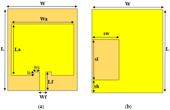
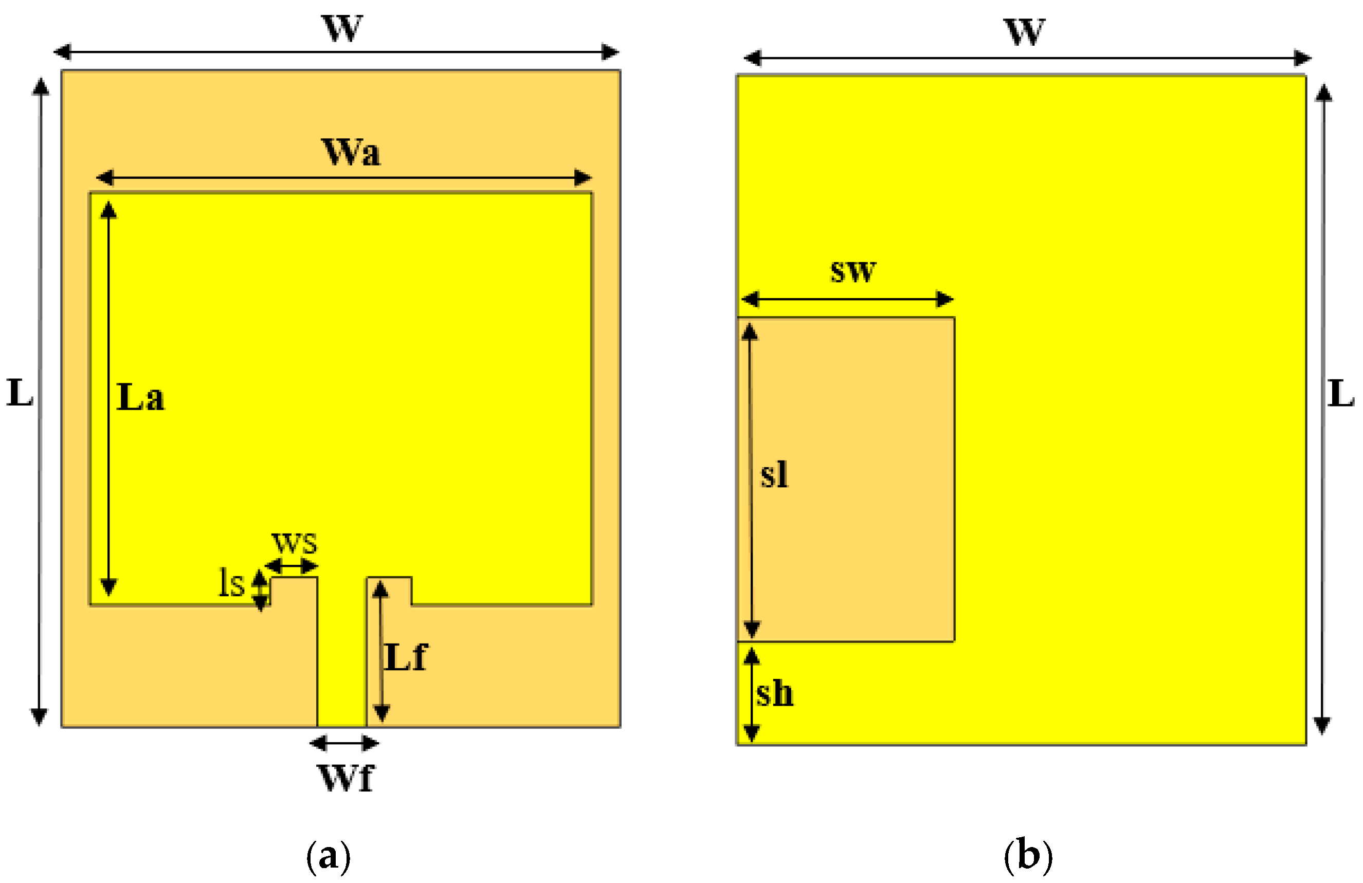
To achieve dual-band operation, a rectangular slot of width sw and length sl was etched in the ground plane at an offset sh (Table 3). The upper band originates from the TM10 mode of the patch identified above; in the presence of the slot, this resonance moves slightly upward (from about 2.36 GHz to about 2.42 GHz) and becomes considerably wider, which is consistent with the lower quality factor of a structure whose ground plane is partly open. The lower band does not exist in the unslotted structure and is therefore introduced by the ground slot; during the parametric study of Section 3.2, its frequency was found to be governed mainly by the slot dimensions and position. A plausible physical interpretation is that the slot interrupts the return current on the ground plane beneath the patch and the feed line and lengthens its path around the slot edges, thereby supporting an additional resonance. Since surface-current distributions are not presented, this interpretation is offered as an explanation consistent with the observed behavior rather than as a demonstrated mechanism; the conclusion established by the results is that the ground slot introduces and controls the lower resonance. This separation of roles leads to a simple design procedure: the patch dimensions are first selected from Equations (10)–(12) to place the upper band, and the slot geometry is then tuned to place the lower band. This approach is advantageous for maintaining a simple, single-layer structure while achieving dual-band operation. The geometry of this antenna is depicted in Figure 1a,b, which show the front and back views, respectively. The optimized slot dimensions were determined through iterative simulations to fine-tune the performance. The geometric parameters of the antenna shown in Figure 1 are presented in Table 3.
Figure 1.
Front (a) and back (b) views of the designed antenna.
3.2. Optimization Process
The slot geometry was optimized using the parametric sweep feature in CST Microwave Studio (CST MWS). This tool allows for systematic variation in the slot dimensions and positions to identify the configuration that minimizes return loss and achieves the desired dual-band operation. Key optimization parameters included slot length and width, slot position, and ground plate modification. The slot dimensions directly affect the lower and upper resonance frequencies. Adjusting the position of the slot relative to the patch center enables fine control over frequency response. Various ground plane configurations were explored to achieve optimal impedance matching and radiation patterns. Starting from the patch dimensions obtained from Equations (10)–(12), the patch and feed dimensions were kept fixed, and the slot length sl, slot width sw and slot offset sh were then varied by parametric sweeps. The objective was to minimize |S11| at 1.75 GHz and 2.45 GHz while keeping both −10 dB bands centered on the target channels; the configuration that best satisfied this objective was retained, and its dimensions are given in Table 3. The use of FR-4 material required careful consideration of losses and substrate thickness to ensure adequate performance.
3.3. Design Considerations
Several design considerations were addressed during the development of the antenna. First, ensuring that the antenna covers the target frequencies with sufficient bandwidth for practical applications was a key priority. Second, balancing gain and efficiency was crucial, particularly due to the lossy nature of the FR-4 substrate. Third, the antenna was designed to be easily manufacturable using standard PCB technology to simplify fabrication. Finally, achieving a good impedance match, typically 50 ohms, was essential to minimize reflection losses and ensure efficient energy transfer. The final design successfully meets these requirements, resulting in a compact, efficient dual-band antenna suitable for RF energy-harvesting applications.
4. Simulation of the Proposed Antenna
The performance of the designed dual-band microstrip patch antenna was evaluated through comprehensive simulations using CST MWS. These simulations focused on key antenna parameters, including reflection coefficient (S11), bandwidth, and radiation patterns, to ensure that the antenna meets the requirements for RF energy-harvesting applications at 1.75 GHz and 2.45 GHz. The obtained results presented in the following subsections indicate that the antenna design meets the requirements for RF energy harvesting in dual-band applications in terms of impedance matching and bandwidth; the radiation characteristics reported below are simulated quantities.
The simulations were carried out in CST MWS (CST Studio Suite 2024) with the time-domain (FIT) solver. The antenna was excited by a waveguide port with a reference impedance of 50 Ω, placed at the substrate edge on the microstrip feed line, and the SMA connector was not included in the model. Open boundary conditions with added free space were applied in all directions, and the far-field quantities were obtained from field monitors at 1.75 GHz and 2.45 GHz. A hexahedral mesh with adaptive mesh refinement was used, and the transient solution was terminated at an energy decay of −40 dB. The patch, feed line and ground plane were modelled as copper with a thickness of 0.035 mm and a conductivity of 5.8 × 10⁷, and the FR-4 substrate with εr = 4.4 and a loss tangent of 0.02.
4.1. Return Loss and Bandwidth Analysis
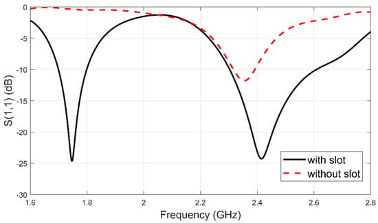
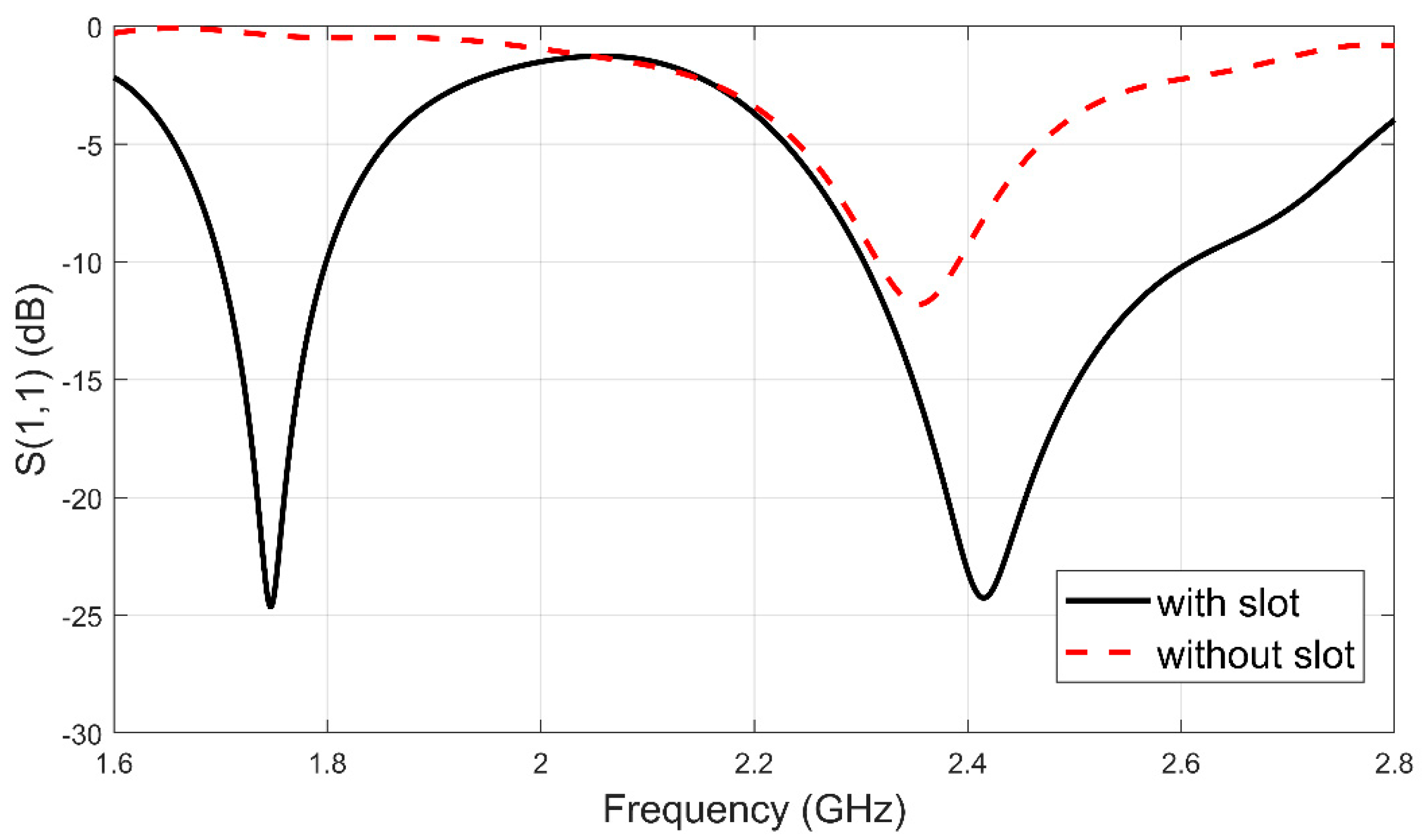
The S11 parameter represents the negative of return loss, which indicates how well the antenna is matched to the input impedance (typically 50 ohms). The goal was to achieve an S11 value of −10 dB or lower at the target frequencies, signifying that at least 90% of the incident power is accepted by the antenna, and at most 10% is reflected back. Simulations were conducted to compare the S11 results before and after incorporating the rectangular slot in the ground plane. As shown in Figure 2, the antenna initially operated as a single-band antenna between 2.32 GHz and 2.39 GHz. After introducing the slot and optimizing its dimensions, the antenna exhibited dual-band behavior, covering 1.7–1.8 GHz (centered at 1.75 GHz) for GSM-1800 uplink and 2.3–2.6 GHz (centered at 2450 MHz) for Wi-Fi. The S11 values at these frequencies were close to −25 dB, indicating good impedance matching and minimal reflection losses. The introduction of the ground slot significantly improved the bandwidth of the antenna. The optimized design achieved a bandwidth of approximately 100 MHz at 1.75 GHz and a bandwidth of approximately 300 MHz at 2.45 GHz. This wide bandwidth ensures robust performance in practical applications, where frequency deviations might occur due to environmental factors or fabrication tolerances. Moreover, the electrical dimensions of the proposed antenna are 0.23λ × 0.27λ × 0.0093λ at 1.75 GHz and 0.33λ × 0.38λ × 0.013λ at 2.45 GHz. The radius of the smallest sphere enclosing the antenna is a ≈ 30.9 mm, which gives ka ≈ 1.13 at 1.75 GHz and ka ≈ 1.58 at 2.45 GHz, k being the free-space wavenumber. Since both values exceed unity, the antenna does not satisfy the conventional criterion of an electrically small antenna (ka < 1) [2] and is therefore described as compact rather than electrically small.
Figure 2.
S11 simulation result of the microstrip patch antenna with and without ground slot.
4.2. Radiation Patterns
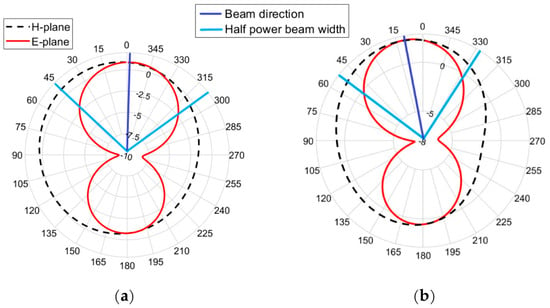
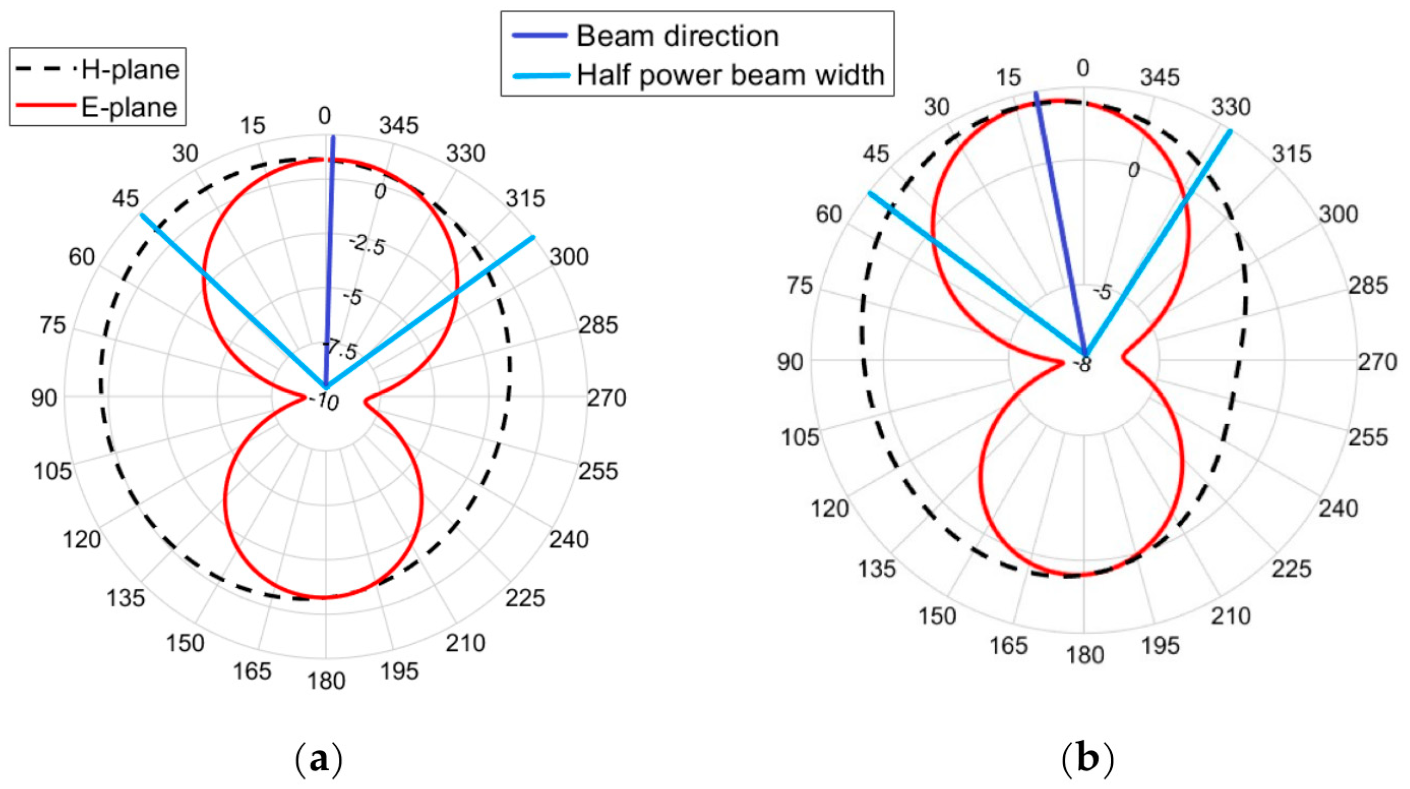
The radiation characteristics of the antenna were analyzed through simulation to determine the distribution of the radiated power at the target frequencies. Figure 3 presents the simulated realized gain patterns in the E- and H-planes as absolute values in dBi, i.e., without normalization; the light-blue lines mark the 3 dB beamwidth and the dark-blue line the main-lobe direction. At 1.75 GHz, the E-plane pattern is bidirectional, with a main-lobe value of 0.912 dBi in the direction of 2.0° and a 3 dB beamwidth of 95.2°, while the H-plane pattern varies only slightly over a wide angular range. The back lobe lies 1.7 dB below the main lobe, which is consistent with radiation through the slotted, partly open ground plane.
Figure 3.
Simulated realized gain patterns (dBi) in the H-plane and E-plane of the proposed dual-band antenna at (a) 1.75 GHz and (b) 2.45 GHz.
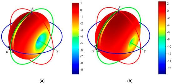
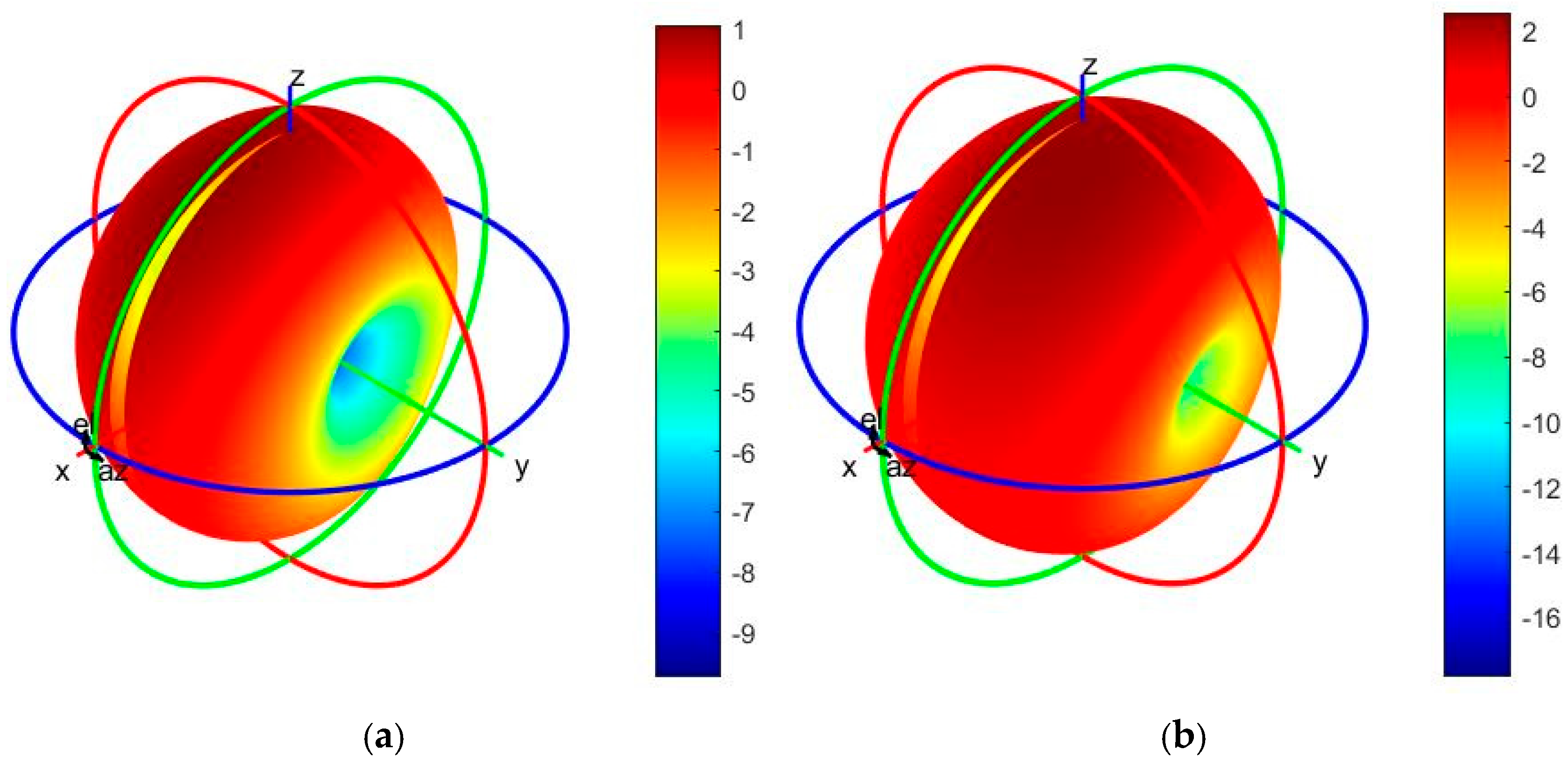
At 2.45 GHz, the E-plane pattern is again bidirectional, with a main-lobe value of 2.49 dBi in the direction of 10.0°, a 3 dB beamwidth of 86.0° and a back lobe 2.0 dB below the main lobe. The higher main-lobe value relative to 1.75 GHz agrees with the realized gains discussed in Section 4.3. The broad beamwidths indicate that, within the two principal planes, the antenna receives with comparable gain over a wide angular range, which is favorable when the direction of arrival of the incident wave is not known in advance. The back lobe and side lobes do not in themselves increase the harvested power; they redistribute the radiated power, and by reciprocity the receiving gain, over a wider range of directions at the expense of the main-lobe gain. Since the patterns are available only in two principal planes and only from simulation, they do not establish omnidirectional reception, and no angular received-power analysis was performed; the discussion of angular coverage is therefore limited to the simulated patterns in Figure 3 and Figure 4. The simulated three-dimensional radiation patterns are presented in Figure 4.
Figure 4.
Simulated three-dimensional radiation patterns of the designed dual-band antenna at (a) 1.75 GHz and (b) 2.45 GHz.
4.3. Efficiency and Gain
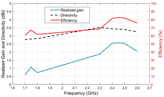
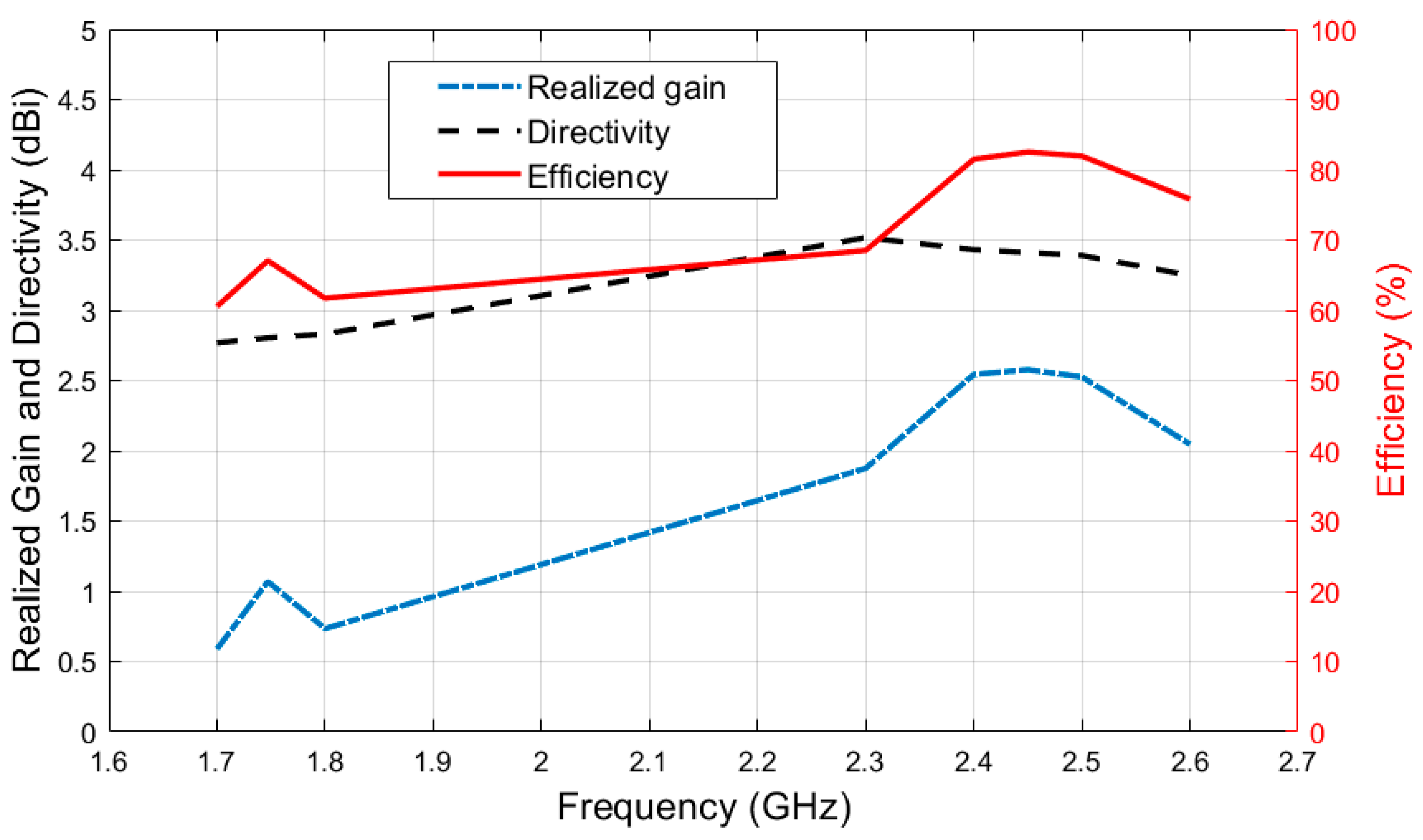
The antenna’s gain, directivity and efficiency were evaluated as critical performance metrics. The simulated realized gain, directivity and calculated efficiency of the proposed antenna presented in Figure 5. As shown in Figure 5, the antenna exhibits simulated peak realized gains of 1.07 dBi at 1.75 GHz and 2.54 dBi at 2.45 GHz, with corresponding directivity values of 2.8 dBi and approximately 3.4 dBi, respectively. The efficiency shown in Figure 5 is the total efficiency of the antenna, ηt = Gr/D, which accounts for conductor, dielectric and mismatch losses; it characterizes the antenna alone and should not be confused with the RF-to-DC conversion efficiency of the harvester introduced in Equation (7). The calculated efficiencies of 68% at 1.75 GHz and 83% at 2.45 GHz indicate that most of the power supplied at the antenna port is radiated rather than dissipated or reflected; by reciprocity, the same efficiency applies in reception. The higher efficiency at 2.45 GHz indicates lower losses in this band. The lower efficiency at 1.75 GHz is reflected in the lower realized gain of this band, which is partly offset by the larger effective aperture at the lower frequency (Section 2.3).
Figure 5.
Simulated realized gain, directivity, and total efficiency of the designed antenna versus frequency.
It should be emphasized that the realized gain, directivity and efficiency in Figure 5, like the patterns in Figure 3 and Figure 4, are simulated quantities; far-field measurements of the prototype were not carried out in this study. Of the factors that make up the realized gain, only the mismatch term is verified experimentally, since the measured S11 agrees closely with the simulation in the upper band and remains below −12 dB at 1.75 GHz (Section 6.1). The radiation efficiency and directivity of the prototype may differ from the simulated values because of the actual losses of the FR-4 laminate, the SMA connector and the fabrication tolerances. Because Emin in Equation (9) is proportional to Gr−1/2, a deviation of ±1 dB in the realized gain changes the field thresholds of Table 2 by about 11–12%. The gains, efficiencies and field thresholds used in Section 2.3 are therefore simulation-based estimates rather than experimentally validated link parameters.
4.4. Polarization
The patch is excited along its resonant length La, so that the radiation of the TM10 mode in the upper band is expected to be linearly polarized along the feed direction, as in a conventional rectangular patch [2]. A comparison of the co-polarized and cross-polarized components, or an equivalent polarization metric, was not evaluated in this study; the polarization purity of the antenna, particularly in the slot-related lower band, has therefore not been quantified. For the linearly polarized emissions of mobile terminals and Wi-Fi access points, the received power depends on the relative orientation through the polarization loss factor p in Equation (3), and the values in Table 2 correspond to the ideal case p = 1.
5. Fabricated Microstrip Antenna
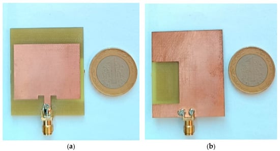
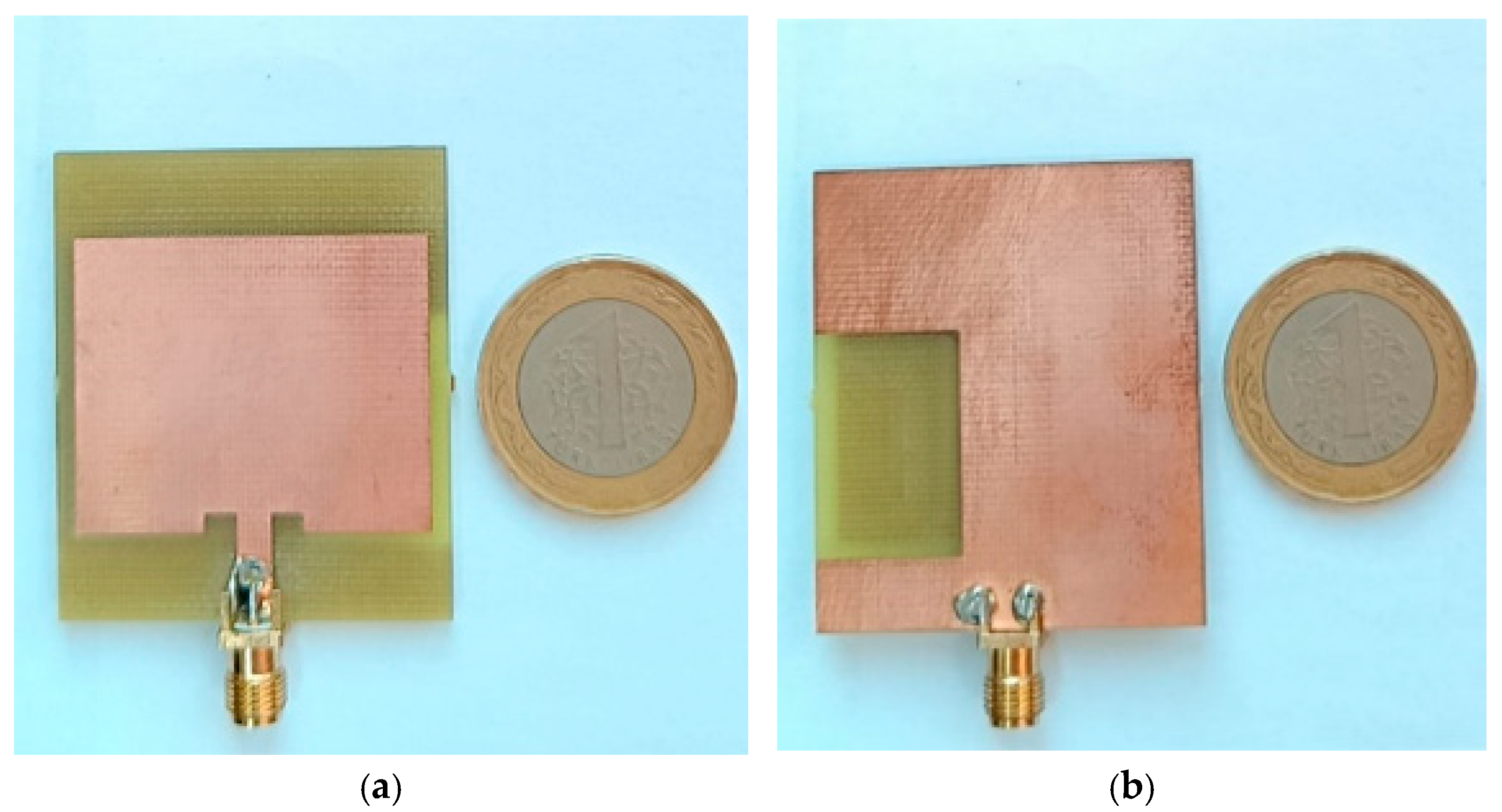
The fabrication of the dual-band microstrip patch antenna began after finalizing the design and optimization process. The antenna was produced using printed circuit board (PCB) technology, known for its accuracy, reproducibility, and cost-effectiveness. The substrate material selected was FR-4, which offers a dielectric constant of 4.4, ensuring stable performance and durability. The optimized design, created in CST Microwave Studio (CST MWS), was exported to Gerber format, the standard file type for PCB manufacturing, and then fabricated through a commercial facility. The front view of the fabricated antenna, shown in Figure 6a, displays the rectangular patch designed to resonate at dual frequencies. The back view, shown in Figure 6b, features the ground plane with a rectangular slot, which was introduced to achieve dual-band operation at 1.75 GHz and 2.45 GHz. The physical dimensions of the antenna, 40 × 47 × 1.6 mm3, match the design specifications. This compact size facilitates integration into low-power harvesting nodes such as IoT sensors, whereas integration into wearable devices would additionally require a flexible substrate.
Figure 6.
Front (a) and back (b) views of the designed and fabricated dual-band antenna.
6. Measurement Results of the Fabricated Antenna
6.1. Reflection Coefficient Measurements
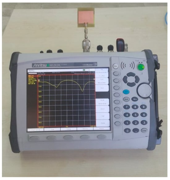
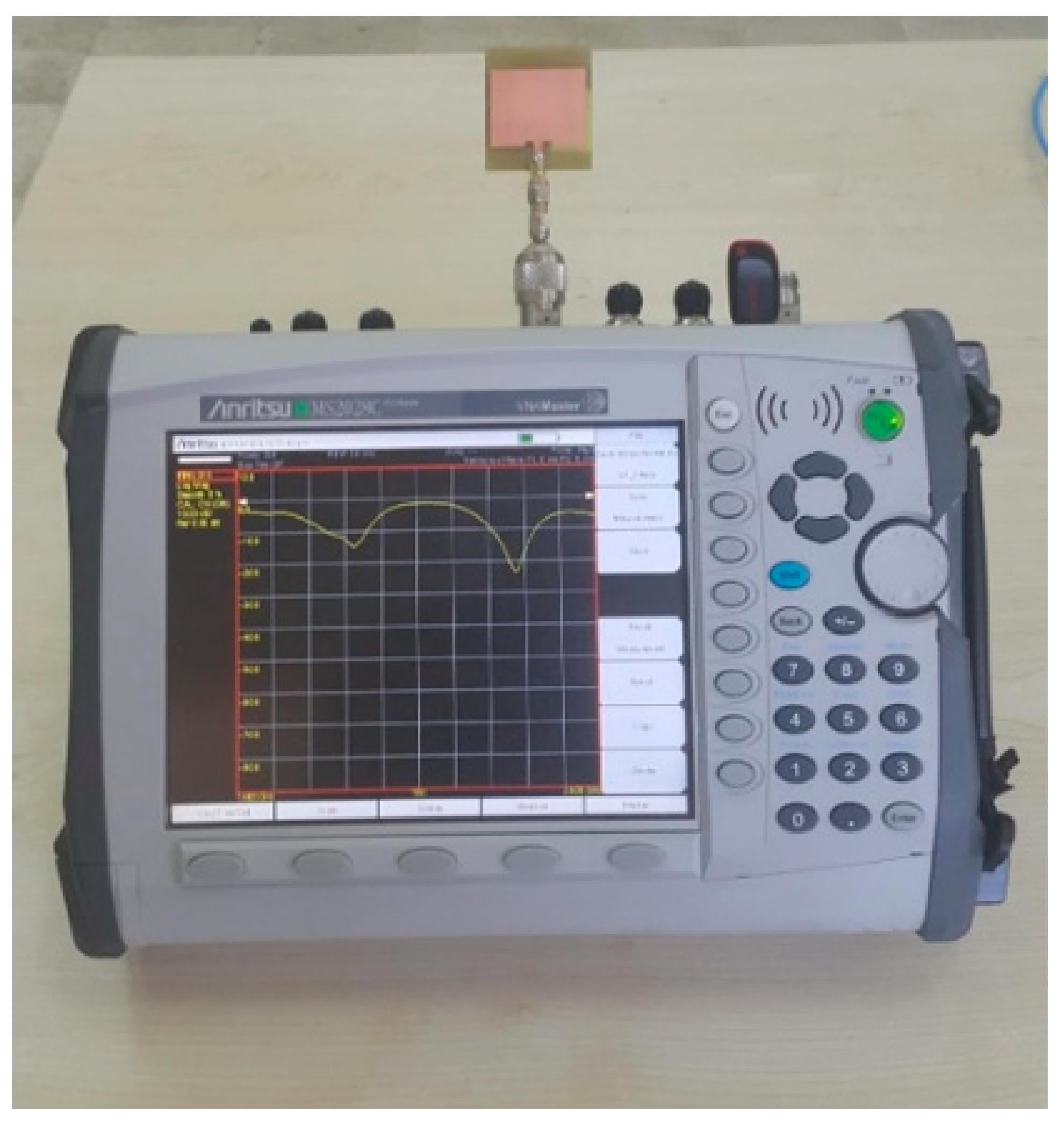
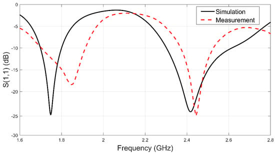
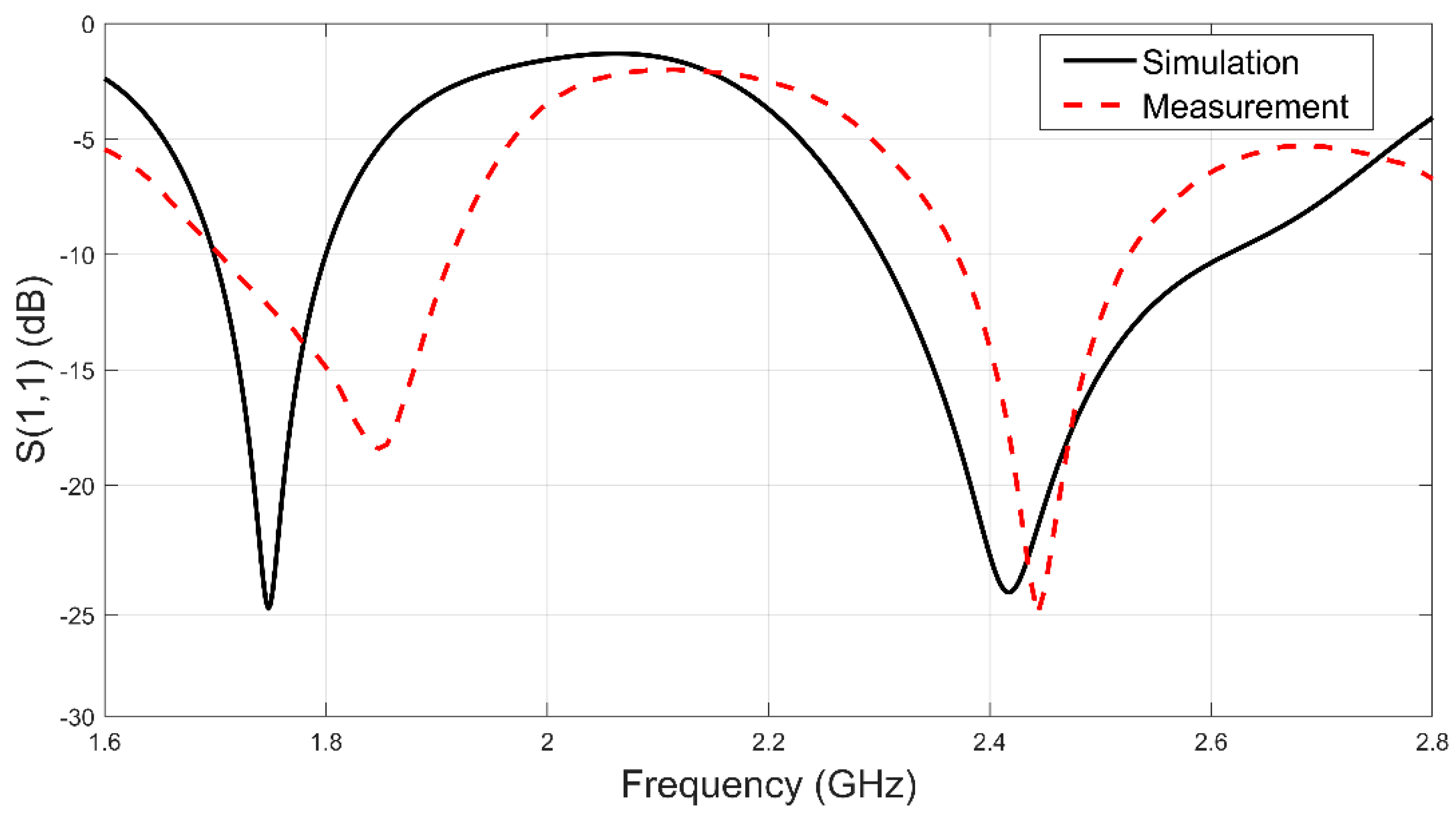
After fabrication, the reflection coefficient of the prototype was measured with an Anritsu MS2028C vector network analyzer (VNA; Anritsu Corporation, Atsugi, Japan), as depicted in Figure 7, while its RF energy-harvesting capability was assessed with the P21XXCSR-EVB evaluation board developed by Powercast Corporation (Pittsburgh, PA, USA) [34] (Section 6.2). Prior to the measurement, a one-port open–short–load (OSL) calibration was performed over the measured frequency range, with the calibration standards connected at the end of the adapter mounted on the VNA test port; this plane defines the measurement reference plane, and the antenna was attached at this plane through its SMA connector without an additional cable (Figure 7). The measured S11 therefore includes the SMA connector and its transition to the microstrip feed line, which are not part of the simulation model. The results, shown in Figure 8, indicate good overall agreement between the measured and simulated S11 responses. In the upper band, the measured S11 reaches a minimum of approximately −25 dB at 2.44 GHz, in close agreement with the simulation. In the lower band, the measured resonance is shifted upward to approximately 1.85 GHz (S11 ≈ −18 dB); nevertheless, the measured S11 at 1.75 GHz is approximately −12 dB and thus remains below the −10 dB threshold. The corresponding mismatch loss, −10log10(1 − |S11|2), is about 0.26 dB at 1.75 GHz and below 0.02 dB at 2.45 GHz, so that the observed shift has only a minor influence on the power delivered to the harvester. Overall, the measured response reproduces the dual-band behavior predicted by the simulation.
Figure 7.
S11 measurement of the fabricated antenna.
Figure 8.
S11 graph of the designed and fabricated dual-band antenna (simulation and measurement results).
The measured −10 dB impedance bandwidths are approximately 210 MHz (1.70–1.91 GHz) in the lower band and 155 MHz (2.37–2.53 GHz) in the upper band, compared with simulated bandwidths of approximately 100 MHz (1.70–1.80 GHz) and 300 MHz (2.30–2.61 GHz). Both measured bands contain the corresponding harvester input channels (1747.5 MHz and 2450 MHz) as well as the GSM-1800 uplink (1710–1785 MHz) and the 2.4 GHz Wi-Fi band (2400–2483.5 MHz). The wide bandwidth ensures that the antenna remains effective even when minor frequency variations occur due to environmental factors or manufacturing tolerances, making it suitable for practical RF energy-harvesting applications.
The differences between the measured and simulated responses, most notably the upward shift of about 100 MHz (about 5.7%) of the lower resonance and the narrower measured upper band, are attributed to factors that could not be characterized individually in this study: fabrication tolerances of the etched patch, feed and slot, the deviation of the FR-4 permittivity from its nominal value of 4.4, and the SMA connector and its transition to the feed line, which are not included in the simulation model. Since no dimensional inspection of the prototype, substrate characterization or connector model is available to separate these effects, they are stated as possible rather than established causes. The analytical model of Section 3.1 nevertheless gives an indication of their relative weight. According to Equations (10)–(12), a change of ±0.1 in εr shifts the patch-mode resonance by about ∓27 MHz (∓1.1%), and a uniform reduction of εr to about 3.9 would be needed to produce a 5.7% upward shift if the lower resonance followed the same dependence. Such a reduction would have moved the upper resonance by a similar fraction, i.e., by about 140 MHz, whereas the measured upper resonance lies within about 25 MHz of the simulated one (2.44 GHz versus approximately 2.42 GHz in Figure 8). A global deviation of the substrate permittivity is therefore unlikely to be the dominant cause of the lower-band shift, which points instead to effects localized at the slot-loaded ground, such as deviations of the etched slot dimensions and the influence of the connector on the ground currents near the feed. The lower band is expected to be particularly sensitive to these effects because its resonance is governed by the slot geometry (Section 3.1 and Section 3.2). Despite these differences, both target channels remain within the measured −10 dB bands, and the overall performance of the fabricated antenna is consistent with the simulated design. Since the lower resonance is governed by the slot geometry, it is also amenable to correction after fabrication; possible tuning approaches are outlined in Section 7.
6.2. Energy Harvesting Under Controlled Illumination
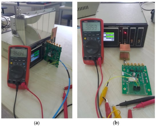
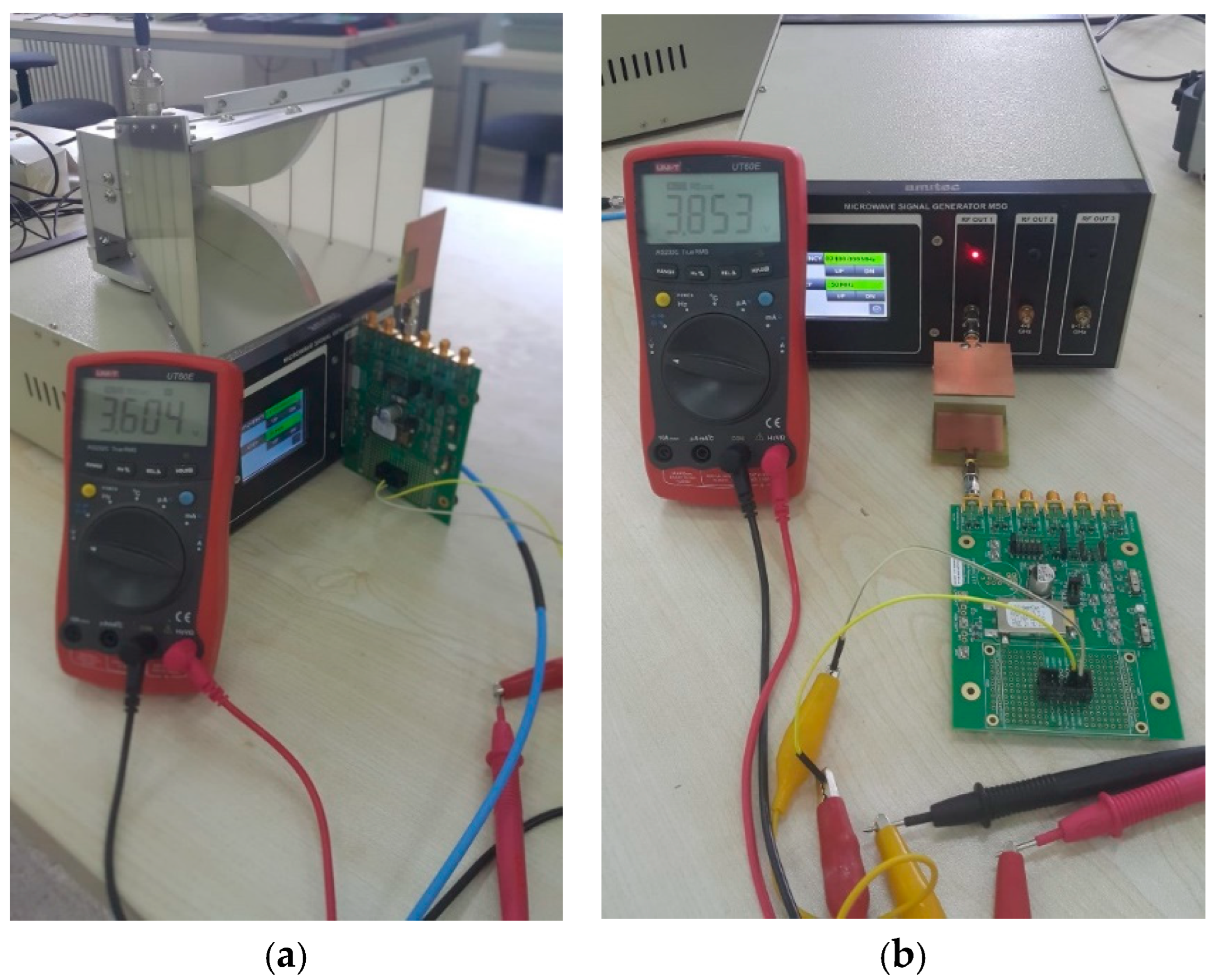
The energy-harvesting capability of the fabricated antenna was examined under controlled illumination using the P21XXCSR-EVB evaluation board (Powercast) [34], which provides dedicated RF inputs for the GSM-1800 uplink (J4, 1710–1785 MHz, centered at 1747.5 MHz) and the 2.4 GHz Wi-Fi band (J6, 2400–2500 MHz, centered at 2450 MHz). The antenna was connected to input J4 for the 1.75 GHz test and to input J6 for the 2.45 GHz test. The output regulator of the board was set to 4.2 V (switch S1), the 1.2 V turn-on threshold of the storage capacitor was selected (jumper JP3), and the DC voltage between the VOUT test point and ground was read with a true-RMS digital multimeter. A continuous-wave (CW) signal was produced by a PLL-synthesized microwave signal generator (Amitec MSG12, Amitec Electronics Ltd. New Delhi, India; 40 MHz–12.4 GHz) with a typical output level of 0 dBm. As shown in Figure 9, two different transmitting antennas were used: a double-ridge horn antenna (Amitec; 1–18 GHz; linear polarization; specified gain 8.5 dBi) at 1.75 GHz and a microstrip patch antenna connected directly to the generator output at 2.45 GHz. In both cases, the fabricated antenna was placed on the boresight of the transmitting antenna, co-polarized with it, and at a short separation (Figure 9). Since these separations are comparable to or shorter than the far-field distances of the transmitting antennas, Equation (4) cannot be used to estimate the incident field. The illumination was therefore characterized through the response of the harvester itself, whose activation threshold is specified by the manufacturer [34]. The test configuration, the activation thresholds and the recorded DC voltages are summarized in Table 4.
Figure 9.
Controlled-illumination harvesting setups and DC voltages read at the board output: (a) 1.75 GHz, with a double-ridge horn antenna as the transmitter; (b) 2.45 GHz, with a microstrip patch antenna connected to the signal generator as the transmitter.
Table 4.
Test configuration, activation thresholds and recorded DC voltages of the controlled-illumination harvesting tests.
The harvester was activated in both bands, and DC voltages of 3.60 V and 3.85 V were read at its output (Figure 9 and Table 4). Since the board provides no output unless the RF power accepted at its input reaches Pmin (Section 2.2), the activation shows that the power delivered by the antenna to a matched load, Pr, reached at least about −13 dBm at 1.75 GHz and −12 dBm at 2.45 GHz; for |Γa| ≤ 0.25 and a harvester input matched to better than −10 dB, the multiple-reflection factor of Equation (6) limits the uncertainty of this inference to about 0.7 dB. This activation, rather than a field value, is the direct experimental result of the test. Through Equation (5), it corresponds to plane-wave-equivalent incident fields of at least the lower bounds Emin of Table 2 (2.51 V/m and 3.33 V/m). Because this correspondence relies on the same effective-aperture relation as Table 2, it does not constitute an independent validation of the field-based model, and at the short separations used here it does not represent the actual local field. Furthermore, since the received power was not quantified, the tests show that the activation condition was met, but not by what margin it was exceeded.
The voltages read at the output are lower than the 4.2 V regulator setting, which follows from the operating cycle of the board described in Section 2.2. The boost converter is enabled only while the storage capacitor discharges from Vmax = 1.25 V to Vmin = 1.02 V, i.e., for about 34 ms per cycle at the 1.2 V threshold setting, and it is then disabled until the capacitor has been recharged by the harvested power [34]. The output therefore consists of regulated pulses separated by recharge intervals in which the output node is not driven by the converter. A multimeter cannot follow pulses of this duration, a limitation also noted by the manufacturer [34], and its reading is expected to lie between the regulated level and the voltage to which the output decays between pulses. The values of 3.60 V and 3.85 V thus demonstrate that the harvester was activated and delivered a DC output in both bands; they do not establish sustained regulated power delivery, nor do they quantify the harvested DC power, because the output current and the pulse repetition rate were not recorded. Such a quantification would require the output to be recorded with an oscilloscope under a defined load, so that the energy delivered per pulse and the repetition rate could be related to PDC through Equation (8).
A test at or beyond the far-field distance of the transmitting antennas, where the incident field could have been obtained from Equation (4), was limited by the available transmitter power. In the far field, the effective isotropic radiated power (EIRP) required to produce a field E at a distance d follows from Equation (4) as PtGt = E2d2/30. Producing only the lower-bound fields of Table 2 requires an EIRP of about 23.2 dBm at 1.75 GHz and 25.7 dBm at 2.45 GHz at d = 1 m, and 6 dB more for each doubling of the distance; an additional margin would be needed to compensate for the idealized assumptions of Table 2. The signal generator used in this study provides a typical output level of 0 dBm, and the manufacturer specifies a single gain of 8.5 dBi for the horn antenna over its 1–18 GHz band. Even when this value is taken as the gain at 1.75 GHz and cable losses are neglected, the attainable EIRP is at most about 8.5 dBm, i.e., approximately 15 dB below the 23.2 dBm required at 1 m, and Equation (4) then gives only about 0.46 V/m at that distance. The lower bound of 2.51 V/m would be reached at about 0.18 m, which corresponds to approximately one wavelength (λ ≈ 0.17 m); since the far-field relation requires a separation much larger than the wavelength in addition to 2D2/λ [2], this distance lies outside the range of validity of Equation (4) irrespective of the horn aperture. The same conclusion holds at 2.45 GHz: even if the patch transmitter had the same gain as the horn, 3.33 V/m would be reached only at about 0.14 m (≈1.1λ), and the attainable EIRP would fall about 17 dB short of the 25.7 dBm required at 1 m. The lower-bound activation fields therefore cannot be produced in the far field with the available equipment, which is why the short-range configuration of Figure 9 was adopted. For the same reason, a mapping of the DC voltage against the incident field would carry limited information with this board, since the output level is fixed by the regulator and the incident power governs only the activation and the pulse repetition rate (Section 2.2).
The uncertainty associated with near-field operation and alignment affects the field-based interpretation of the tests rather than the observed activation. In the reactive and radiating near-field regions, the receiving characteristics of the antenna differ from its far-field gain, the field over the antenna aperture is non-uniform, and mutual coupling with the transmitting antenna is present; the plane-wave-equivalent field is therefore defined only as an equivalent quantity, and its deviation from the local field cannot be quantified without a full-wave model of each setup. Residual misalignment between the two linear polarizations reduces p to cos2ψ, ψ being the misalignment angle; for ψ = 10° and 20°, p = 0.97 and 0.88, so that the equivalent field required for activation exceeds Emin by about 1.5% and 6.4%, respectively. Irrespective of these factors, the activation of the harvester shows that the power accepted at its input reached Pmin in both tests.
6.3. Implications for Operation in Ambient Fields
Ambient harvesting measurements were not performed in this study, and the experimental validation is therefore restricted to the controlled illumination described in Section 6.2. The link budget of Section 2.3 nevertheless allows for the conditions under which the present antenna–harvester combination can operate in ambient fields to be assessed. The J4 input of the harvester accepts only the GSM-1800 uplink band (1710–1785 MHz) [34], in which the sources are mobile terminals rather than base stations; downlink emissions at 1805–1880 MHz, although partly within the measured lower band of the antenna, fall outside this input. For an LTE terminal transmitting at its maximum output power of 23 dBm [35], Equation (4) with an isotropic terminal antenna gives about 2.5 V/m at a distance of 1 m in free space, so that the 2.51 V/m bound of Table 2 is approached only within about 1 m of a terminal transmitting continuously at full power. In the 2.4 GHz band, the EIRP of wideband transmitters is limited to 20 dBm in Europe [36], which corresponds to about 1.7 V/m at 1 m; the 3.33 V/m bound is thus exceeded only within about 0.5 m of an access point radiating at this limit, and only during its transmissions. Since both types of sources transmit intermittently and their emissions depend on traffic, the time-averaged power available at larger distances is lower still. These estimates agree with Table 2, according to which fields of 0.1–1 V/m deliver 8–31 dB less power than the harvester requires, and with city-wide surveys in which even harvesters designed for typical ambient input levels could be operated at only about half of the surveyed urban locations [32]. Consequently, no harvester output is expected with the present commercial module at typical indoor or outdoor locations away from a transmitter. In such environments, the relevant quantity is the RF power received by the antenna, which can be exploited by rectifiers of higher sensitivity, by combining the power of several bands or antennas, or by arrays of larger effective aperture. Measurements of the received ambient power at representative indoor and outdoor locations are therefore identified as a necessary next step (Section 7).
7. Conclusions and Suggestions for Future Studies
In this study, a dual-band microstrip patch antenna for RF energy-harvesting applications was designed, simulated, fabricated, and tested. The antenna, constructed on an FR-4 substrate, uses a rectangular ground-plane slot to introduce a lower resonance at 1.75 GHz in addition to the fundamental patch mode, which provides the upper band at 2.45 GHz. Simulations in CST Microwave Studio yielded S11 values close to −25 dB, bandwidths of approximately 100 MHz and 300 MHz, peak realized gains of 1.07 dBi and 2.54 dBi, and total efficiencies of 68% and 83% at the two frequencies; since the radiation characteristics were not measured, these quantities remain simulation-based. The measured −10 dB bands (approximately 1.70–1.91 GHz and 2.37–2.53 GHz) contain both target channels, although the lower resonance of the prototype is shifted upward by about 100 MHz. The analytical link-budget model indicated that, for polarization alignment, a matched harvester input and the simulated peak realized gains, plane-wave-equivalent incident fields of at least about 2.5 V/m at 1.75 GHz and 3.3 V/m at 2.45 GHz are needed to reach the minimum input power of the P21XXCSR-EVB harvester; these values are lower bounds, which polarization mismatch, non-boresight incidence and harvester mismatch increase. Under controlled short-range illumination, the harvester was activated in both bands, which shows that the RF power delivered by the antenna reached its minimum input power, and DC voltages of 3.60 V and 3.85 V were read at its output. These results show that the proposed antenna is a suitable compact and low-cost receiving element for RF energy harvesting when it operates in sufficiently strong RF fields, such as in the vicinity of a transmitter, or is combined with a rectifier of adequate sensitivity. Its use in wearable devices remains a possible application that would require a flexible substrate and an on-body evaluation.
Future work can focus on several directions to enhance the performance and applicability of the dual-band antenna. Material optimization can be pursued by exploring alternative substrate materials with lower losses and higher efficiency, such as Rogers RO4003 or flexible materials suitable for wearable applications. The design can also be extended to a multi-band configuration, allowing the antenna to harvest energy from additional RF sources, including 5G bands or other wireless communication frequencies. Another important step is the integration of a complete rectenna system (antenna and rectifier), optimized for maximum RF-to-DC conversion efficiency, to improve overall energy-harvesting performance. Miniaturization techniques can be employed to reduce the antenna size while maintaining its performance, making it more suitable for compact and embedded applications. Additionally, ambient measurements in urban, rural and industrial environments, in which the received RF power is recorded together with the harvester response, and far-field measurements of the radiation pattern, realized gain and polarization of the prototype are planned; the antenna can also be combined with low-threshold rectifiers so that the field levels typical of such environments can be exploited. Alternative ground-slot geometries (e.g., L-shaped, U-shaped, or annular slots) and a systematic comparison with other miniaturization techniques also deserve investigation, as does a diplexed or dual-port configuration that would allow for both harvester inputs to be fed simultaneously. Because the lower resonance of the prototype was measured about 100 MHz above its design value and is governed mainly by the slot geometry, post-fabrication tuning of this band is also of practical interest. A first step would be to re-simulate the antenna with the measured permittivity of the FR-4 laminate, the actual etched dimensions, and a model of the SMA connector, so that the cause of the shift can be identified and the slot dimensions of a subsequent prototype compensated accordingly. On an existing board, the lower resonance could be adjusted by small modifications of the slot length or width, made by trimming the ground copper or by covering part of the slot with conductive copper tape, or by bridging the slot with a lumped capacitor, whose reactive loading lowers the slot-related resonance without changing the patch geometry; the effect of each adjustment on the upper band would then have to be verified by measurement. Replacing the fixed capacitor with a varactor diode would extend this approach to continuous electronic tuning, by which detuning caused by nearby objects or an enclosure could also be compensated, although the required bias network and the additional losses would have to be weighed against the small mismatch loss of about 0.26 dB observed at 1.75 GHz in the present prototype. Finally, integrating the antenna with supercapacitors or rechargeable batteries can create a comprehensive energy harvesting and storage solution for continuous low-power device operation.
Author Contributions
H.A., D.I. and H.Ö.: Conceptualization, Methodology, Software, Visualization, Investigation, Writing—Original draft preparation. S.E.: Data curation, Validation, Supervision, Resources, Writing—Review & Editing. E.A.: Project administration, Supervision, Resources, Writing—Review & Editing. All authors have read and agreed to the published version of the manuscript.
Funding
This research received no external funding.
Data Availability Statement
All related data are available within the manuscript. The CST simulation model is available from the corresponding author upon reasonable request.
Conflicts of Interest
The authors declare no conflicts of interest.
References
- Özmen, H.; Ekinci, S.; Izci, D. Boosted Arithmetic Optimization Algorithm with Elite Opposition-Based Pattern Search Mechanism and Its Promise to Design Microstrip Patch Antenna for WLAN and WiMAX. Int. J. Model. Simul. 2023, 45, 264–279. [Google Scholar] [CrossRef] [Scilit]
- Balanis, C.A. Antenna Theory: Analysis and Design; John Wiley & Sons: Hoboken, NJ, USA, 2015; ISBN 1119178991. [Google Scholar]
- Misra, G.; Agarwal, A.; Agarwal, K. Design and Performance Evaluation of Microstrip Antenna for Ultra-Wideband Applications Using Microstrip Feed. Am. J. Electr. Electron. Eng. 2015, 3, 93–99. [Google Scholar]
- Kasar, O.; Kahriman, M.; Gozel, M.A. Application of Ultra Wideband RF Energy Harvesting by Using Multisection Wilkinson Power Combiner. Int. J. RF Microw. Comput.-Aided Eng. 2019, 29, e21600. [Google Scholar] [CrossRef] [Scilit]
- Cansız, M. 915 MHz Taşıyıcı Frekansında RF Enerji Hasatlama. DÜMF Mühendis. Derg. 2019, 10, 91–98. [Google Scholar] [CrossRef] [Scilit]
- Sahoo, S.; Mishra, L.P.; Mohanty, M.N. Optimization of Z-Shape Microstrip Antenna with I- Slot Using Discrete Particle Swarm Optimization (DPSO) Algorithm. Procedia Comput. Sci. 2016, 92, 91–98. [Google Scholar] [CrossRef] [Scilit]
- Özmen, H.; Kurt, M.B. Radar-Based Microwave Breast Cancer Detection System with a High-Performance Ultrawide Band Antipodal Vivaldi Antenna. Turk. J. Electr. Eng. Comput. Sci. 2021, 29, 2326–2345. [Google Scholar] [CrossRef] [Scilit]
- Amador, M.; Rouco, A.; Albuquerque, D.; Pinho, P. Overview of Vivaldi Antenna Selection for Through-Wall Radar Applications. Sensors 2024, 24, 6536. [Google Scholar] [CrossRef] [Scilit] [PubMed]
- Chen, H.; Zhang, L.; Chen, Y.; Mao, C.; Li, W.; He, Y. Reverse Design of a Dual-Band Microstrip Patch Antenna Based on Binary Particle Swarm Optimization. In Proceedings of the 2023 International Applied Computational Electromagnetics Society Symposium (ACES-China), Hangzhou, China, 15–18 August 2023; IEEE: Piscataway, NJ, USA, 2023; pp. 1–3. [Google Scholar]
- Tsao, Y.-F.; Desai, A.; Hsu, H.-T. Dual-Band and Dual-Polarization CPW Fed MIMO Antenna for Fifth-Generation Mobile Communications Technology at 28 and 38 GHz. IEEE Access 2022, 10, 46853–46863. [Google Scholar] [CrossRef] [Scilit]
- Boudjerda, M.; Reddaf, A.; Kacha, A.; Hamdi-Cherif, K.; Alharbi, T.E.A.; Alzaidi, M.S.; Alsharef, M.; Ghoneim, S.S.M. Design and Optimization of Miniaturized Microstrip Patch Antennas Using a Genetic Algorithm. Electronics 2022, 11, 2123. [Google Scholar] [CrossRef] [Scilit]
- Wang, Z.; Liu, S.; Dong, Y. A Compact, Broadband, Monopole-Like Endfire Antenna with Reconfigurable Patterns for 5G Applications. IEEE Trans. Antennas Propag. 2022, 70, 7199–7204. [Google Scholar] [CrossRef] [Scilit]
- Xu, J.; Hong, W.; Jiang, Z.H.; Zhang, H.; Wu, K. Low-Profile Wideband Vertically Folded Slotted Circular Patch Array for Ka -Band Applications. IEEE Trans. Antennas Propag. 2020, 68, 6844–6849. [Google Scholar] [CrossRef] [Scilit]
- Islam, M.T.; Mahmud, M.Z.; Islam, M.T.; Kibria, S.; Samsuzzaman, M. A Low Cost and Portable Microwave Imaging System for Breast Tumor Detection Using UWB Directional Antenna Array. Sci. Rep. 2019, 9, 15491. [Google Scholar] [CrossRef] [Scilit] [PubMed]
- Khan, N.U.; Ullah, S.; Khan, F.U.; Merla, A. Development of 2400–2450 MHz Frequency Band RF Energy Harvesting System for Low-Power Device Operation. Sensors 2024, 24, 2986. [Google Scholar] [CrossRef] [Scilit] [PubMed]
- Linge, P.U.; Pandey, A.; Gerges, T.; Duchamp, J.-M.; Benech, P.; Verdier, J.; Lombard, P.; Mieyeville, F.; Cabrera, M.; Tsafack, P.; et al. Evaluation of Recycled Cardboard Paper as an Eco-Friendly Substrate for Rectenna and Ambient Radio Frequency Energy Harvesting Application. Electronics 2024, 13, 2499. [Google Scholar] [CrossRef] [Scilit]
- En-Naghma, W.; Halaq, H.; El Ougli, A. Analysis, Design, and Optimization Based on Genetic Algorithms of a Highly Efficient Dual-Band Rectenna System for Radiofrequency Energy-Harvesting Applications. Results Eng. 2024, 23, 102739. [Google Scholar] [CrossRef] [Scilit]
- Cansiz, M.; Altinel, D.; Kurt, G.K. Efficiency in RF Energy Harvesting Systems: A Comprehensive Review. Energy 2019, 174, 292–309. [Google Scholar] [CrossRef] [Scilit]
- Contreras, A.; Rodríguez, B. Optimization of a Novel Rectenna for RF Energy Harvesting at 2.45 GHz. Wirel. Pers. Commun. 2021, 119, 2451–2467. [Google Scholar] [CrossRef] [Scilit]
- Wagih, M.; Hillier, N.; Yong, S.; Weddell, A.S.; Beeby, S. RF-Powered Wearable Energy Harvesting and Storage Module Based on E-Textile Coplanar Waveguide Rectenna and Supercapacitor. IEEE Open J. Antennas Propag. 2021, 2, 302–314. [Google Scholar] [CrossRef] [Scilit]
- Surender, D.; Khan, T.; Talukdar, F.A. A Hexagonal-Shaped Microstrip Patch Antenna with Notch Included Partial Ground Plane for 2.45 GHz Wi-Fi Band RF Energy Harvesting Applications. In Proceedings of the 2020 7th International Conference on Signal Processing and Integrated Networks (SPIN), Noida, India, 27–28 February 2020; IEEE: Piscataway, NJ, USA, 2020; pp. 966–969. [Google Scholar]
- Yathavi, T.; Maunasree, K.; Meenakshi, G.B.; Malika, M.V.; Santhoshini, M. RF Energy Harvesting for Low Power Applications. In Proceedings of the 2021 10th International Conference on Internet of Everything, Microwave Engineering, Communication and Networks (IEMECON), Jaipur, India, 1–2 December 2021; IEEE: Piscataway, NJ, USA, 2021; pp. 1–6. [Google Scholar]
- Benkalfate, C.; Ouslimani, A.; Kasbari, A.-E.; Feham, M. A New Compact Triple-Band Triangular Patch Antenna for RF Energy Harvesting Applications in IoT Devices. Sensors 2022, 22, 8009. [Google Scholar] [CrossRef] [Scilit] [PubMed]
- Aziz, A.; Farhan, M.; Sharif, A.; Ijaz, U.; Safdar, N. A Novel High Permittivity Ceramic-Silicone Composite Substrate-Based Antenna for Energy Harvesting. AEU-Int. J. Electron. Commun. 2024, 184, 155427. [Google Scholar] [CrossRef] [Scilit]
- El Batal, K.; Douhi, S.; Eddiai, A.; Das, S.; Cherkaoui, O.; Mazroui, M. Design and Performance Analysis of a Low-Profile Dual-Band Antenna with Low Specific Absorption Rate Using Textile Materials for Wearable and RF Energy Harvesting Applications. J. Electron. Mater. 2024, 53, 8141–8153. [Google Scholar] [CrossRef] [Scilit]
- Yang, L.; Zhou, Y.J.; Zhang, C.; Yang, X.M.; Yang, X.-X.; Tan, C. Compact Multiband Wireless Energy Harvesting Based Battery-Free Body Area Networks Sensor for Mobile Healthcare. IEEE J. Electromagn. RF Microw. Med. Biol. 2018, 2, 109–115. [Google Scholar] [CrossRef] [Scilit]
- Lu, P.; Yang, X.-S.; Wang, B.-Z. A Two-Channel Frequency Reconfigurable Rectenna for Microwave Power Transmission and Data Communication. IEEE Trans. Antennas Propag. 2017, 65, 6976–6985. [Google Scholar] [CrossRef] [Scilit]
- Khemar, A.; Kacha, A.; Takhedmit, H.; Abib, G. Design and Experiments of a Dual-band Rectenna for Ambient RF Energy Harvesting in Urban Environments. IET Microw. Antennas Propag. 2018, 12, 49–55. [Google Scholar] [CrossRef] [Scilit]
- Quddious, A.; Abbasi, M.A.B.; Tahir, F.A.; Antoniades, M.A.; Vryonides, P.; Nikolaou, S. UWB Antenna with Dynamically Reconfigurable Notch Band Using Rectenna and Active Booster. IET Microw. Antennas Propag. 2019, 13, 2046–2052. [Google Scholar] [CrossRef] [Scilit]
- Hamad, A.R.; Al-Adhami, A.; Elmunim, N.A.; Alibakhshikenari, M.; Virdee, B.; Hamad, H.S.; Jayanthi, R.; Mariyanayagam, D.; Lubangakene, I.; Kumar, S.; et al. Rectenna Design Optimized by Binary Genetic Algorithm for Hybrid Energy Harvesting Applications Across 5G Sub-6 GHz Band. Radio Sci. 2025, 60, e2024RS008154. [Google Scholar] [CrossRef] [Scilit]
- Aslan, H.; Izci, D.; Özmen, H.; Ekinci, S.; Ma’arif, A. Geometry-Optimized Design and Experimental Validation of a Compact 2.4 GHz Microstrip Patch Antenna for RF Energy Harvesting. Int. J. Robot. Control Syst. 2026, 6, 1957–1971. [Google Scholar]
- Piñuela, M.; Mitcheson, P.D.; Lucyszyn, S. Ambient RF Energy Harvesting in Urban and Semi-Urban Environments. IEEE Trans. Microw. Theory Tech. 2013, 61, 2715–2726. [Google Scholar] [CrossRef] [Scilit]
- Pozar, D.M. Microwave Engineering, 4th ed.; John Wiley & Sons: Hoboken, NJ, USA, 2012; ISBN 978-0-470-63155-3. [Google Scholar]
- Powercast Corporation. P21XXCSR-EVB Powerharvester® Chipset Reference Design Evaluation Board—Datasheet; Powercast Corporation: Pittsburgh, PA, USA, 2018; Available online: https://www.powercastco.com/hubfs/WP%20PDFs/P21XXCSR-EVB-Datasheet-v2.1-1.pdf (accessed on 16 October 2026).
- 3GPP TS 36.101 V17.16.0; Evolved Universal Terrestrial Radio Access (E-UTRA); User Equipment (UE) Radio Transmission and Reception (Release 17). 3rd Generation Partnership Project: Sophia Antipolis, France, 2025. Available online: https://www.3gpp.org/dynareport/36101.htm (accessed on 23 October 2026).
- ETSI EN 300 328 V2.2.2; Wideband Transmission Systems; Data Transmission Equipment Operating in the 2,4 GHz Band; Harmonised Standard for Access to Radio Spectrum. European Telecommunications Standards Institute: Sophia Antipolis, France, 2019.

Disclaimer/Publisher’s Note: The statements, opinions and data contained in all publications are solely those of the individual author(s) and contributor(s) and not of MDPI and/or the editor(s). MDPI and/or the editor(s) disclaim responsibility for any injury to people or property resulting from any ideas, methods, instructions or products referred to in the content. |
© 2026 by the authors. Licensee MDPI, Basel, Switzerland. This article is an open access article distributed under the terms and conditions of the Creative Commons Attribution (CC BY) license.