


Abstract
This paper presents the design, fabrication, and experimental validation of a switched back-to-back E-slotted antenna system for bidirectional wireless relay applications. The proposed antenna integrates two identical E-slotted microstrip patches placed on opposite sides of a single-layer FR4 substrate, together with a PIN diode-based SPDT switching circuit. The switching circuit dynamically routes the RF signal to either antenna element, enabling controllable bidirectional beam switching without additional structural layers. A prototype was fabricated and its performance was verified using a vector network analyzer and a custom-built outdoor radiation pattern measurement setup. The measured resonant frequencies of 2410 MHz and 2418 MHz for the two switching states show good agreement with the simulated value of 2420 MHz. The antenna achieves a measured impedance bandwidth of 3.68% and a simulated peak gain of 5.6 dBi, outperforming several comparable designs reported in the literature. The measured radiation patterns also closely match the simulation results. To demonstrate practical applicability, the antenna was integrated into an active relay node and tested in a non-line-of-sight environment. The system achieved average packet delivery ratios of 89.88% and 86.94% for the short-range and long-range scenarios, respectively. These results confirm that the proposed switched back-to-back antenna system offers a compact, cost-effective, and reliable solution for bidirectional wireless relay applications.
1. Introduction
Modern wireless communication networks, such as Wireless Local Area Networks (WLAN) and the Internet of Things (IoT), are rapidly expanding. These systems frequently operate within the crowded 2.4 GHz ISM band. Maintaining strong and reliable signal coverage is one of the major challenges. As network boundaries grow, wireless relays and repeaters have become essential components to overcome signal degradation and eliminate dead zone problems. One of the critical requirements for these relay systems is efficient bidirectional communication. In order to achieve this aim, communication nodes must be able to transmit and receive signals in opposite directions. As a natural result, reconfigurable antennas have gained significant attention for their ability to dynamically control radiation patterns. Back-to-back antenna configurations are highly suited for wireless relay applications among various approaches. They naturally enable effective beam switching between opposite directions. This capability is very important for managing bidirectional communication links in complex environments.
In recent years, numerous studies in the literature have focused on optimizing back-to-back antenna configurations for wireless relay applications. Consequently, various innovative designs and switching techniques have been introduced to achieve efficient bidirectional communication. Iwasaki developed a compact, CPW-fed back-to-back rectangular patch array that successfully achieves an omnidirectional radiation pattern with a 6-degree beam-tilt, making it highly suitable for microcellular and WLAN applications [1]. Hu et al. [2] presented a dual-beam active microstrip leaky-wave antenna array capable of switching between different radiation modes simply by adjusting the bias voltage of the Gunn diodes, eliminating the need for external RF switching elements. Vian and Popović [3] proposed an antenna design that successfully utilizes optically controlled PIN diodes for fast transmit/receive switching. In [4], a back-to-back repeater antenna uses MEMS-reconfigurable parasitic elements to dynamically improve isolation between the transmitter and receiver. A passive high-impedance surface (HIS) is employed in [5] to reduce coupling by absorbing electromagnetic energy. In [6,7], a planar Yagi-Uda antenna employing PIN diodes on parasitic elements was proposed to switch the end-fire radiation pattern between two opposite directions. A back-to-back patch antenna design with proximity-coupled feeds has been presented in [8] to generate bi-directional radiation with orthogonal polarizations. A back-to-back microstrip patch antenna utilizing a single-pole double-throw (SPDT) PIN diode circuit has been proposed in [9,10] to achieve switchable hemispherical radiation patterns in opposite directions. In [11], a compact bidirectional same-sense circularly polarized antenna was designed using slot-coupled back-to-back patches with a single feeding line. In [12], a protocol-independent, full-duplex RF repeater is proposed, utilizing orthogonal back-to-back patch antennas to achieve high transmit-receive isolation. In [13], a compact four-port MIMO antenna system utilizing back-to-back cylindrical dielectric resonator antennas was presented to achieve bi-directional pattern diversity. In [14], a pattern-reconfigurable antenna utilizing back-to-back magnetic dipoles was proposed to achieve wide-angle beam steering by altering the states of the feed ports. Recently, a reconfigurable antenna employing a diode-loaded electric-inductive-capacitive resonator was introduced to achieve diverse end-fire radiation states [15]. A compact back-to-back microstrip antenna has been proposed to simultaneously achieve broadband omnidirectional energy harvesting and bi-directional wireless power transfer [16]. Eissa and Sukhanov [17] demonstrated that deploying a passive back-to-back antenna system can artificially induce multipath propagation to improve the channel matrix quality in line-of-sight MIMO environments. A compact UHF-RFID repeater utilizing two closely spaced microstrip antennas with opposite circular polarization handedness was proposed in [18] to achieve high inter-antenna isolation and extend the interrogation range. In [19], a pattern and polarization reconfigurable circularly polarized antenna utilizing multiple PIN diodes was proposed to achieve bidirectional beam switching. In a recent study [20], a dual-band back-to-back planar inverted-F antenna (PIFA) system is presented, utilizing etched slots on the ground plane to achieve high inter-port isolation at the 2.4 and 5 GHz bands. Furthermore, Panda et al. [21] proposed an electronically controllable 4-element array antenna for sub-6 GHz applications, integrating switch-line phase shifters and varactor diodes to achieve both discrete and continuous beam steering. Additionally, Cheng et al. [22] demonstrated a 20-GHz switched beam antenna integrated with an RF MEMS SPDT switch on a quartz substrate to electrically steer the beam between two opposite directions. Recent advancements in passive bidirectional antennas have also explored various multiband and wideband configurations. For instance, a tri-band bidirectional antenna has been developed for 2.4/5 GHz WLAN and Ku-band applications [23]. Furthermore, a low-profile wideband circularly polarized metasurface-integrated dipole antenna has been developed for bidirectional wireless applications, achieving LHCP and RHCP radiation in opposite directions over the 4.0–6.5 GHz band [24], while ultra-thin S-slot configurations have recently been proposed to realize compact bidirectional radiation for 5G communications [25]. Despite these structural advancements in passive designs, achieving active and dynamically controllable beam switching without complex profiles remains a primary requirement for efficient wireless relay nodes. Despite all these developments, several of these studies face notable limitations including multi-layered structural profiles [4,5,8,11,13,16] high fabrication costs [6,7,22], and relatively low radiation gains [9,10,15,19]. Additionally, many designs rely on complicated switching mechanisms [2,3,14,21] to achieve bidirectional communication, and some of them completely lack beam-switching capabilities [1,12,16,17,18,20,23,24,25].
This study presents the design and implementation of a switched back-to-back E-slotted antenna system. The proposed architecture integrates an SPDT switching circuit and two microstrip antennas facing opposite directions on a double-sided FR4 substrate. Both the front-side and bottom-side antennas have an E-slotted design. The bottom antenna is energized through a via placed along its microstrip feed line. Acknowledging the inherently narrow-band nature of microstrip patches, the system is specifically optimized for a resonant frequency of 2.42 GHz. The simulations were performed by incorporating the manufacturer-provided S-parameters of the PIN diodes into the design phase. For all simulations, we used COMSOL Multiphysics (Version 5.6) with RF Module. Following the successful numerical evaluations, a prototype was fabricated. Dynamic beam-switching operations of the proposed antenna were controlled using an Arduino Nano microcontroller. The entire system was mounted on a custom 3D-printed pedestal to enable reliable S11 and radiation pattern measurements. We observed good agreement between simulated and measured results. Furthermore, a real-world communication scenario was designed using nRF24L01 transceiver modules to provide a proof of concept. This setup was deployed in a non-line-of-sight (NLOS) environment at the Nevsehir Haci Bektas Veli University Campus. Eventually, direct transmitter-receiver communication was physically blocked. Custom embedded software for the microcontroller was developed to operate the fabricated antenna system as an active relay node. Comprehensive short-range and long-range performance tests confirmed that the proposed system effectively bridges the communication gap. As expected, the short-range tests outperformed the long-range tests, exhibiting a higher mean packet delivery ratio and lower standard deviation across multiple measurements collected over a defined time interval. These results validate the reliability of the system and practical applicability as a bidirectional wireless repeater. Consequently, by avoiding expensive multi-layered profiles and complicated switching components, this work provides a straightforward yet highly effective alternative. In this study, a switched antenna system has been designed, developed and practically validated that offers a cost-effective, reliable, and easily implementable solution for bidirectional wireless relay applications.
The remainder of this paper is organized as follows. Section 2 describes the design of the switched back-to-back E-slotted antenna, including the design evolution of the antenna element, the PIN diode model, and the SPDT switching circuit, followed by the integrated system. Section 3 presents the simulation, measurement, and experimental results, covering the fabrication and measurement setups, S11 and radiation pattern results, gain and efficiency, a comparison with the literature, and the real-world NLOS field tests of the relay node. Section 4 discusses the findings and limitations of the work, and Section 5 concludes the paper.
2. Design of Switched Back-to-Back E-Slotted Antenna
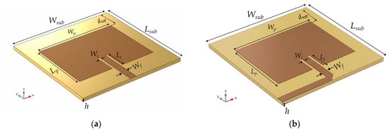
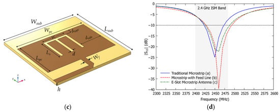
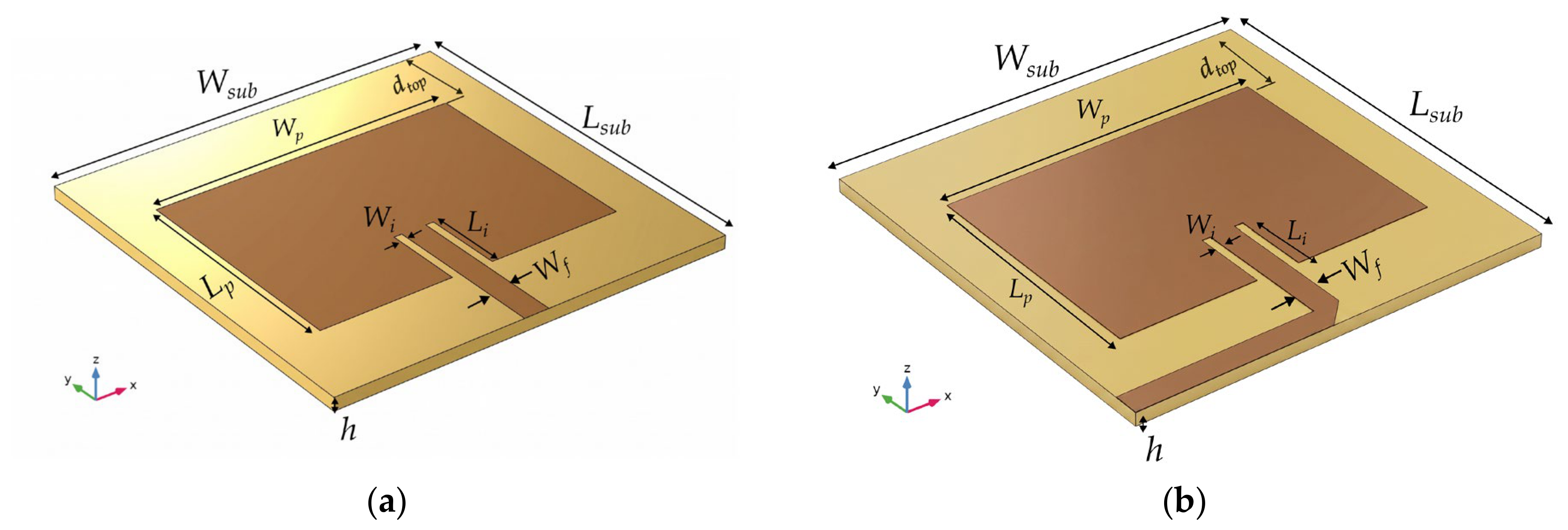
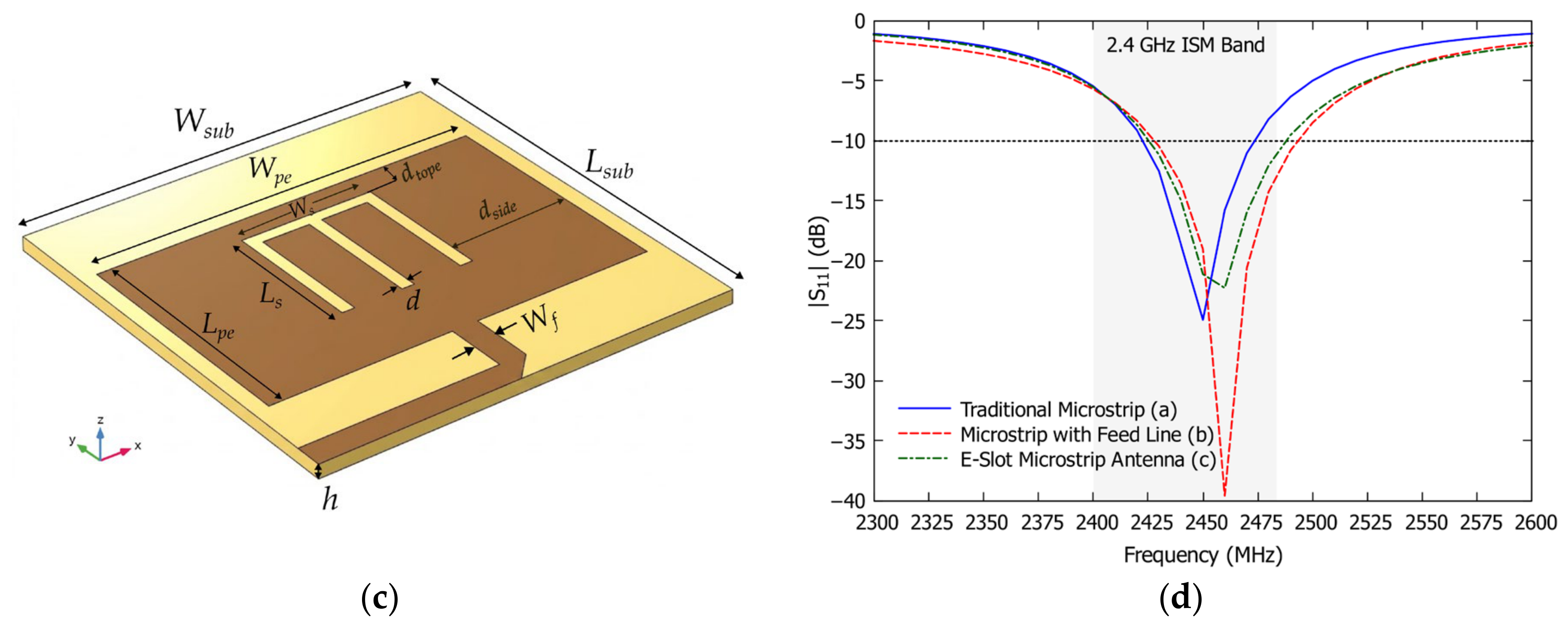
Figure 1 illustrates the step-by-step design evolution of the proposed switched back-to-back E-slotted antenna. Initially, a conventional microstrip patch antenna is designed to resonate within the 2.4 GHz ISM band, as shown in Figure 1a. In this first stage, the exact resonant frequency is 2.45 GHz as depicted in Figure 1d. In the second stage, a 50 Ω transmission line is extended and bent as shown in Figure 1b. This modification slightly shifts the resonant frequency to 2.46 GHz. In the third stage, as seen in Figure 1c, an E-shaped slot is etched into the radiating patch. This transition to an E-slotted design introduces additional tuning parameters beyond the conventional patch length, width, and feed point location. To determine the optimal dimensions of the E-slot—namely the slot length (Ls), overall slot width (Ws), slot gap thickness (d), and the distance from the top edge (dtope)—an initial layout was created and subjected to a rigorous parametric analysis. The study revealed how each parameter uniquely influences the performance of the antenna: smaller Ls values shift the resonant frequency lower, while larger values shift it higher. Decreasing dtope shifts the resonance lower, whereas moving the slot closer to the feed line (larger dtope) shifts the frequency higher, degrades bandwidth, and reduces resonance depth. Adjusting Ws showed that larger widths shift the frequency slightly lower, while smaller widths push it out of the ISM band entirely, sometimes splitting the resonance into two unintended bands. Finally, narrower slot gaps (d) shift the frequency lower and improve the matching depth, while thicker gaps shift it higher and make the resonance shallower. By systematically evaluating these four extra structural variables, the design gains significantly greater flexibility and precision, allowing the resonant frequency to be placed exactly in the center of the 2.4 GHz ISM band with optimal impedance matching. Finally, Figure 1d presents the comparative |S11| reflection coefficient graphs for all three design iterations, demonstrating the tuning progression. The geometric parameters of the final individual E-slot antenna design are given in Table 1.
Figure 1.
The design evolution of the proposed antenna element: (a) conventional microstrip patch antenna for the 2.4 GHz ISM band, (b) microstrip patch antenna with a bent extended transmission line, (c) final E-slotted patch antenna, and (d) comparative |S11| performance of the three sequential design stages.
Table 1.
The geometric parameters of the final E-slot antenna design.
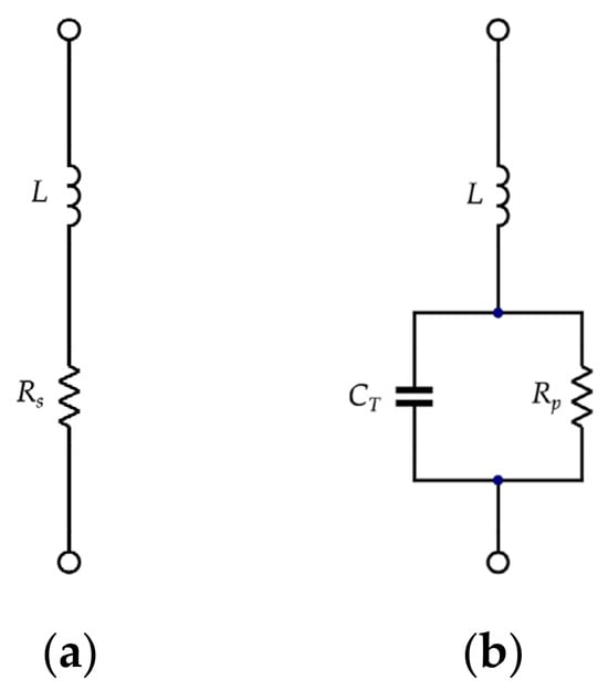
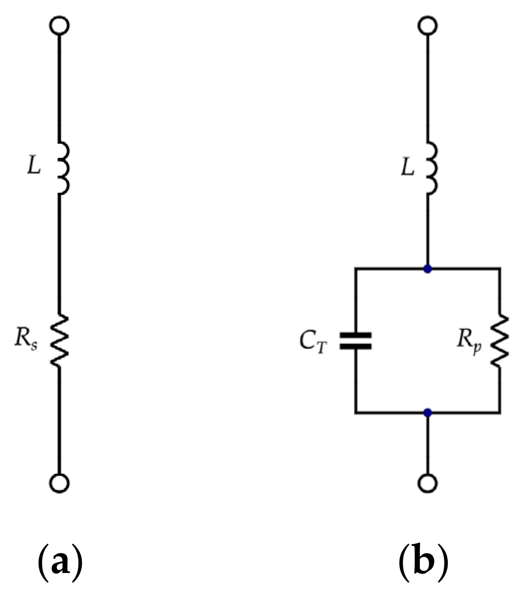
PIN diodes serve as fundamental building blocks in reconfigurable antenna designs due to their low loss and fast switching capabilities in RF and microwave applications. Their distinct impedance characteristics under forward and reverse bias conditions enable dynamic control over the resonance and radiation properties of the antenna. This fundamental behavior can be represented by the simplified equivalent circuit models presented in Figure 2. However, for the electromagnetic simulations, the measured S11 data files provided directly by the manufacturer were utilized as high-fidelity behavioral models [26]. Utilizing measured S-parameters is a standard approach because they directly provide the accurate frequency-dependent response of the physical device. As demonstrated in the literature, simplified equivalent circuit approximations may fail to capture complex high-frequency effects [27]. Accordingly, for the design simulations conducted in the COMSOL environment, the S11 data files of the BAR64-02V PIN diode provided by the manufacturer were integrated into the antenna structure. To model the switching operation, the 0.1 V reverse-bias data was used for the OFF state, and the 10 mA forward-current data for the ON state.
Figure 2.
Equivalent circuit models of a PIN diode under (a) forward bias and (b) reverse bias.
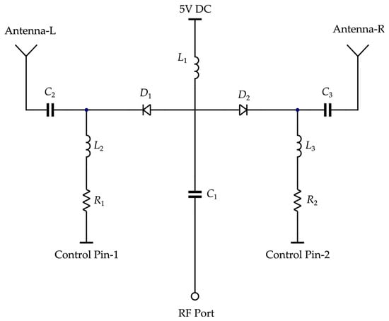
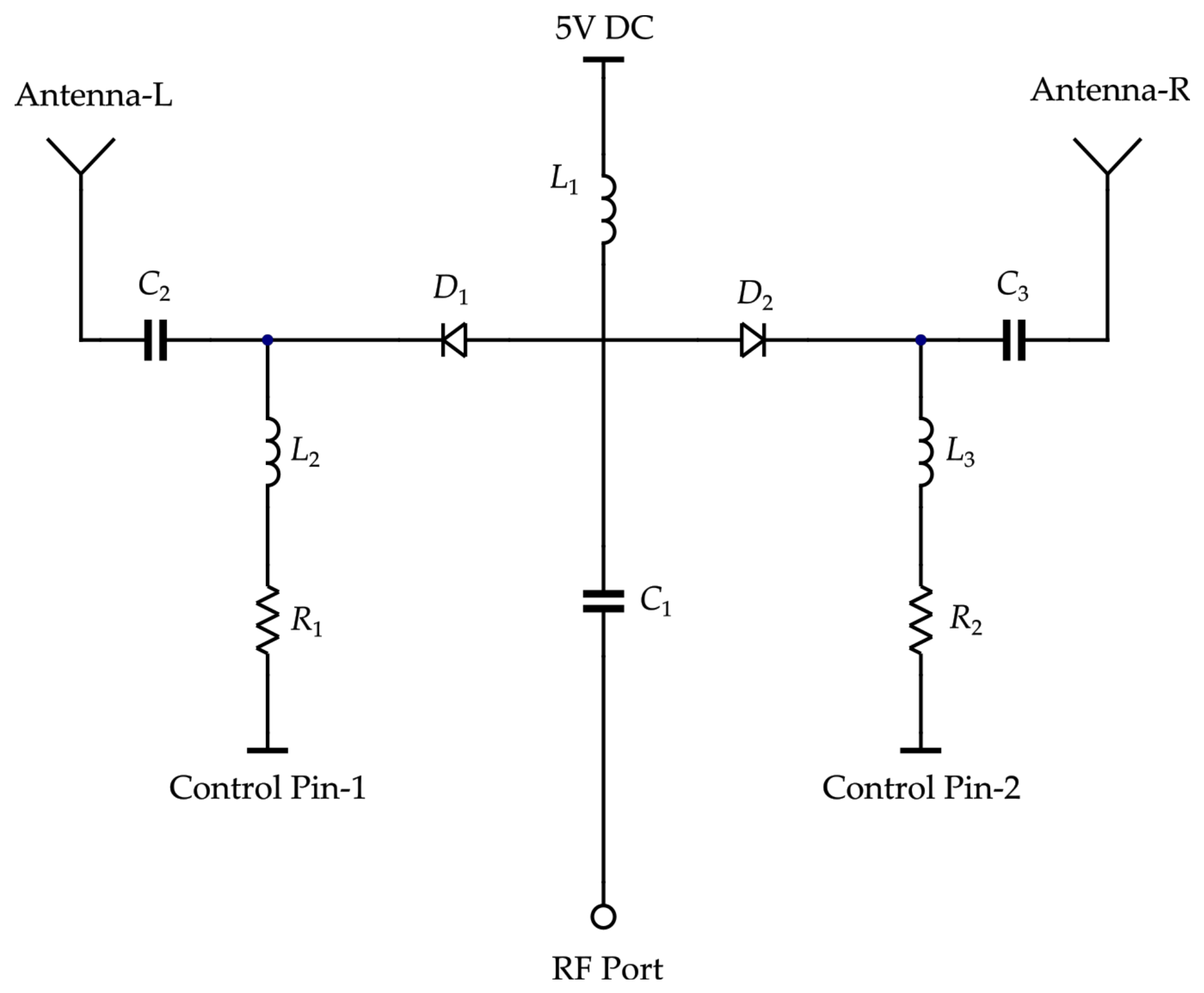
The schematic presented in Figure 3 details an RF SPDT switching circuit configured with PIN diodes D1 and D2 to direct a signal from the RF Port to either the left antenna (Antenna-L) or the right antenna (Antenna-R). The inductors (L1, L2, L3) in the circuit act as RF chokes that isolate the 5V DC biasing supply from the high-frequency RF path. Correspondingly, the capacitors (C1, C2, C3) serve as DC blocks that prevent the DC voltage from reaching the RF ports and antennas. The active RF path is selected by grounding the appropriate control pin. Grounding Control Pin-1 activates D1 to route the signal to Antenna-L, while grounding Control Pin-2 activates D2 to route the signal to Antenna-R.
Figure 3.
Schematic diagram of the PIN diode-based SPDT RF switch for the back-to-back antenna system.
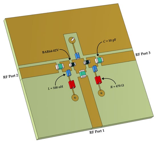
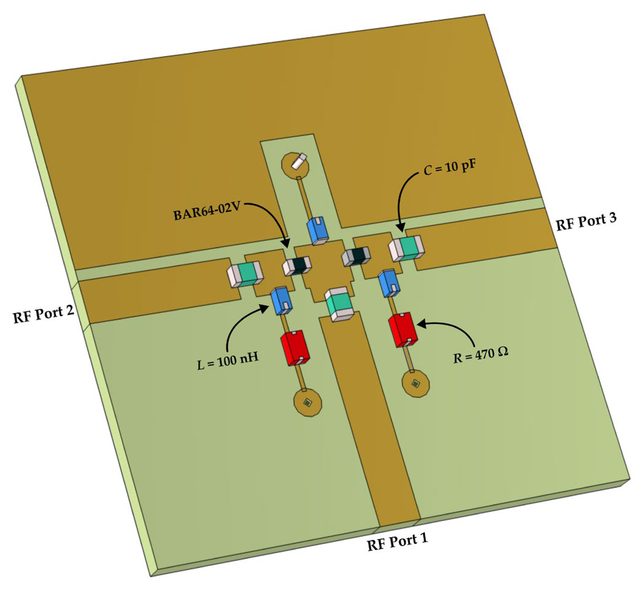
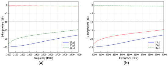
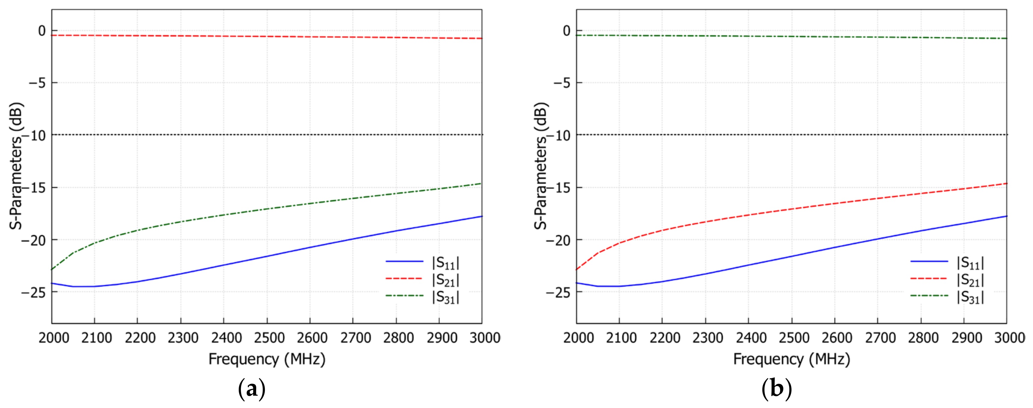
The physical layout of the previously analyzed SPDT switching circuit on an FR4 substrate is presented in Figure 4. To achieve the desired 50-ohm characteristic impedance matching, the width of the RF transmission lines on the structure is set to 3.1 mm. To verify its operational performance, the simulated S-parameters are presented in Figure 5. In both switching states, the input reflection coefficient |S11| remains well below −15 dB across the frequency band, which indicates a very good impedance matching. As shown in Figure 5a, when RF Port 2 is active, the S21 parameter is close to 0 dB, demonstrating low insertion loss. Simultaneously, S31 drops below −15 dB, ensuring high isolation for the inactive port. Conversely, when RF Port 3 is activated as shown in Figure 5b, S31 approaches 0 dB for signal transmission, while S21 falls below −15 dB for isolation. These symmetric S-parameter results confirm that the proposed SPDT switch successfully and accurately routes the RF signal to the desired port.
Figure 4.
Physical layout design of the SPDT switching circuit on the FR4 substrate.
Figure 5.
Simulated S-parameters of the proposed SPDT switch when (a) RF Port 2 is ON and RF Port 3 is OFF, and (b) RF Port 3 is ON and RF Port 2 is OFF.
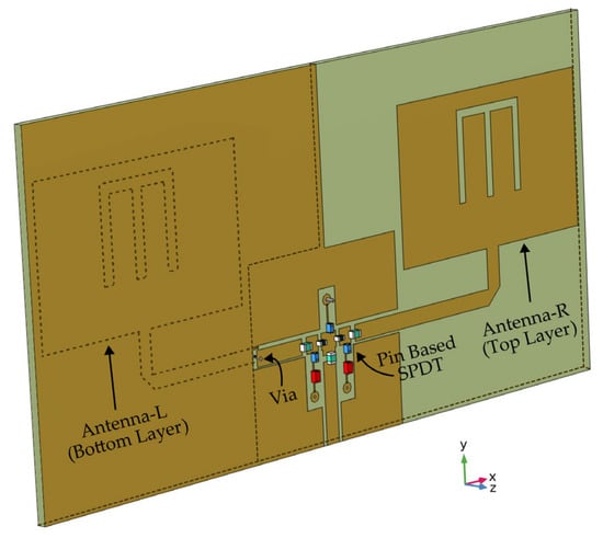
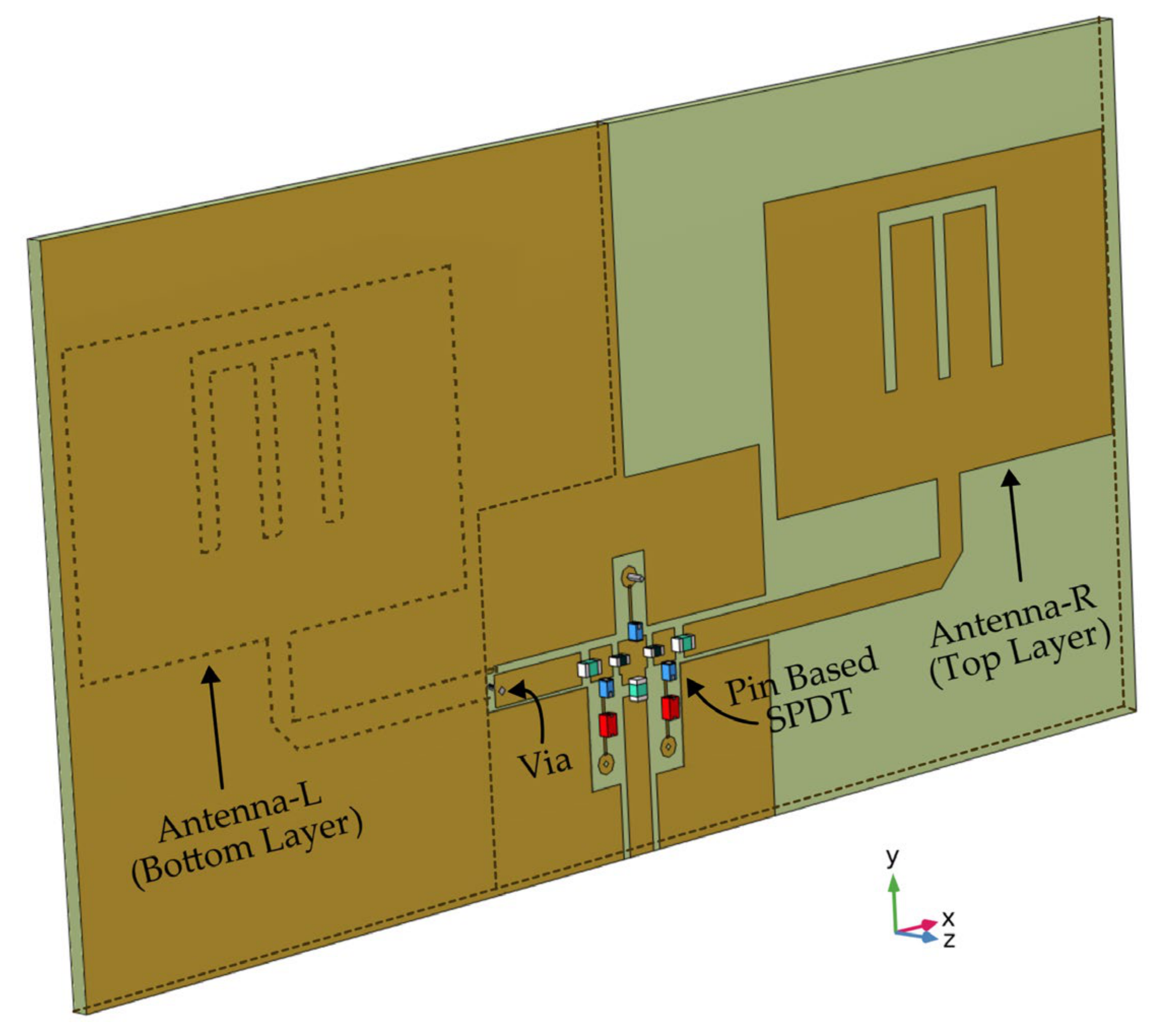
Following the individual development of the E-slotted antenna and the PIN diode SPDT switch, these two units are combined to form the complete back-to-back antenna system. As illustrated in Figure 6, the final system integrates the central switching circuit with two identical back-to-back E-slot microstrip antennas on a 135 mm × 67 mm FR4 board. In this layout, the right antenna (Antenna-R) is positioned on the top layer of the substrate, whereas the left antenna (Antenna-L) is placed on the bottom layer. A structural via is utilized to connect the central switch to the antenna located on the bottom layer. This integrated design allows the system to effectively route the RF signal to either the top or bottom antenna based on the selected operational state. Additional parametric sweep simulations were carried out after the structural formation of the integrated design to set the resonant frequency of both antennas to the intended 2.42 GHz. Following this optimization process, the new geometric parameters of the E-slotted patch antennas (in mm) are Wpe = 46.02, Lpe = 29.35, Ws = 16, Ls = 16.85, d = 1.5, dtope = 3.23, dside = 15.01, Wf = 3.11 and h = 1.6.
Figure 6.
Final system design consisting of identical back-to-back E-slot microstrip antennas integrated with the SPDT switching circuit.
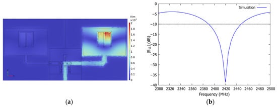
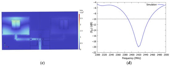
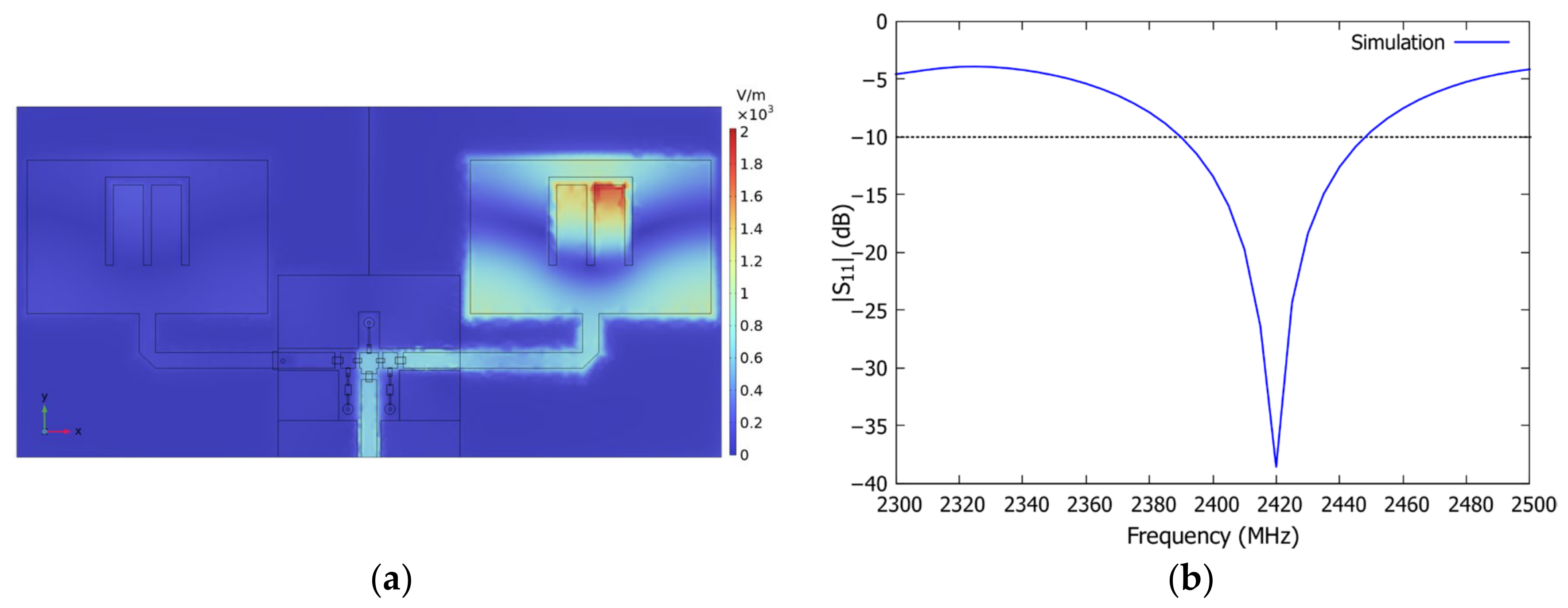
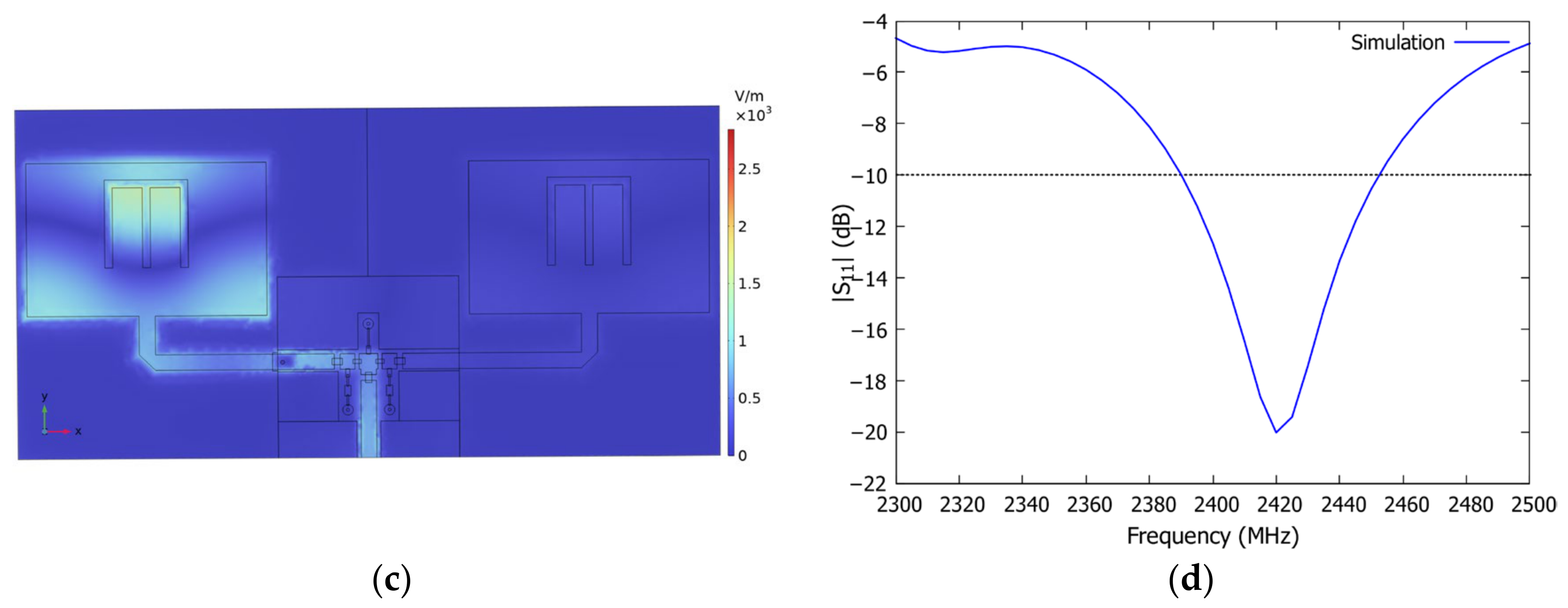
Figure 7 illustrates the simulated performance of the final integrated system for both switching states. Figure 7a and Figure 7b present the electric field distribution and the reflection coefficient in dB when Antenna-R is activated, respectively. The electric field is intensely concentrated on Antenna-R and the graph confirms a deep resonance at the targeted 2.42 GHz. Conversely, Figure 7c,d show the response of the system when Antenna-L is switched on. In this state, the electric field successfully shifts to Antenna-L and the corresponding reflection coefficient maintains stable operation at the same desired frequency point. These results demonstrate that the integrated SPDT switch effectively routes the signal to the selected antenna while maintaining proper impedance matching.
Figure 7.
Simulated performance of the integrated back-to-back antenna system: (a) the electric field distribution and (b) the corresponding reflection coefficient () when Antenna-R is active. (c) The electric field distribution and (d) the reflection coefficient when Antenna-L is active.
3. Simulation, Measurement and Experimental Results
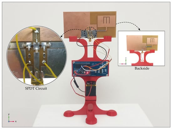
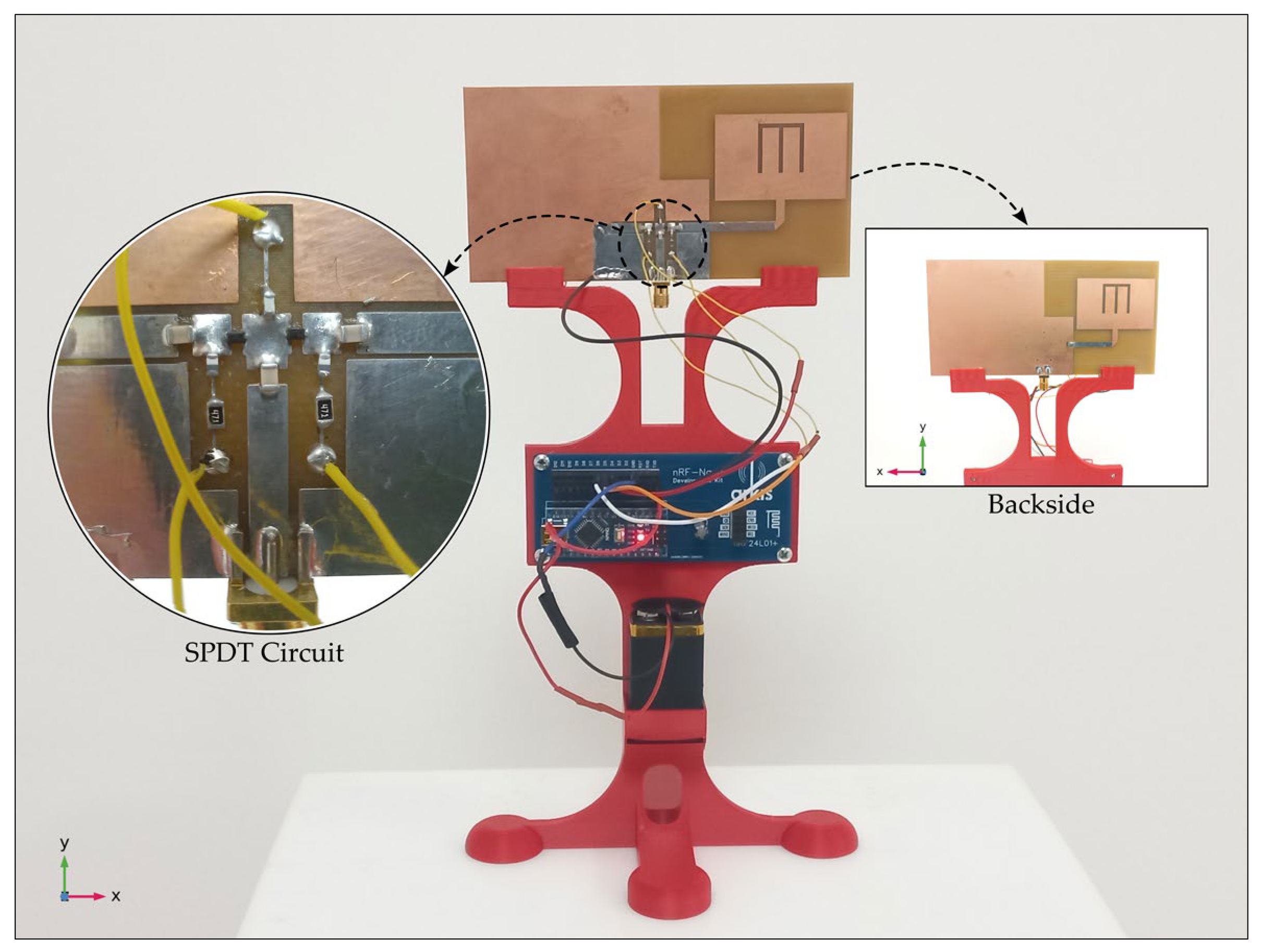
The designed antenna was fabricated using a double-sided FR4 substrate, as shown in Figure 8. Derinmotion Cube 3D MX (Derinmotion, Ankara, Turkey) milling machine was used for the manufacturing process. Afterward, the PIN diode, resistor, capacitor, and inductor components included in the simulation design were soldered. An Arduino Nano (Arduino, Ivrea, Italy) microcontroller was utilized to provide the necessary DC bias voltages for the PIN diode switching operations. The 4th, 5th and 6th digital pins of the microcontroller were used for this task. The system was designed to be controlled in two different ways. It can be switched either by serial data received via the USB port or manually by a rocker switch. The rocker switch was connected to the 9th digital pin of the microcontroller in input pull-up mode. This manual switching method was used temporarily during the radiation pattern measurement process. The switching system was powered by a 9V battery. Finally, the entire system was mounted on a 3D-printed pedestal designed in FreeCAD (Version 1.0.1) as presented in Figure 8.
Figure 8.
Photograph of the fabricated switched back-to-back E-slotted antenna mounted on a 3D-printed pedestal with the controlling unit. Insets show the close-up view of the SPDT circuit and the backside of the antenna.
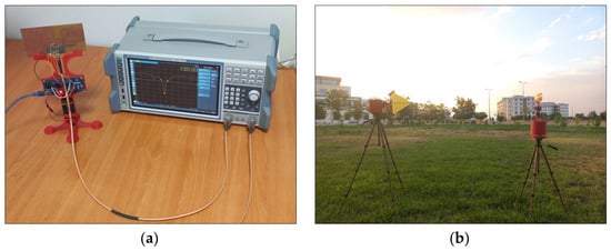
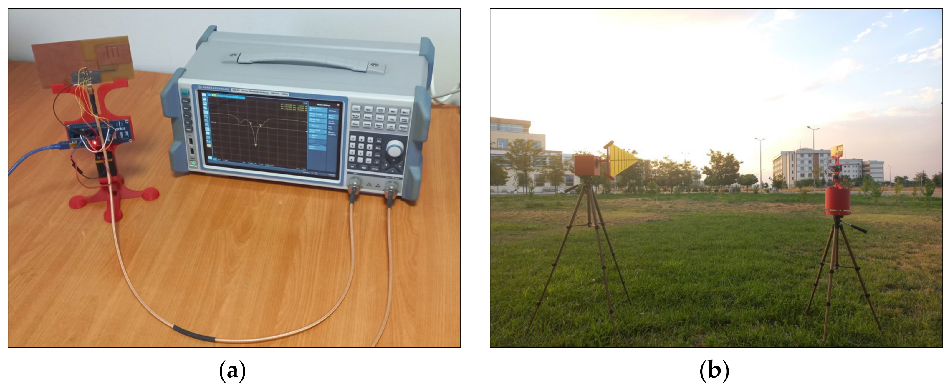
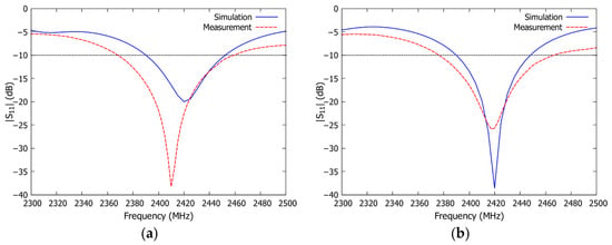
The S11 parameter of the antenna system was measured using an R&S ZNLE3 vector network analyzer (VNA), as shown in Figure 9a. The normalized radiation pattern of the proposed antenna was measured using a custom-built outdoor measurement system, illustrated in Figure 9b. This system mainly consists of a transmitter and a receiver unit. The transmitter includes an ADF4356-based wideband signal synthesizer and a 5 dBi Log-Periodic Dipole Array (LPDA) antenna, while the receiver unit comprises the antenna under test connected to an AD8318 logarithmic RF detector. Both units are powered by an internal lithium-ion battery equipped with a battery management system, enabling fully portable and untethered operation during field measurements. The receiver unit is housed within a cylindrical platform capable of rotating 360° in the azimuth plane. Both units are controlled by microcontrollers and the entire system is managed using Bluetooth Low Energy (BLE) from a central computer.
Figure 9.
Measurement setups: (a) S11 measurement using a vector network analyzer and (b) custom-built outdoor radiation pattern measurement system.
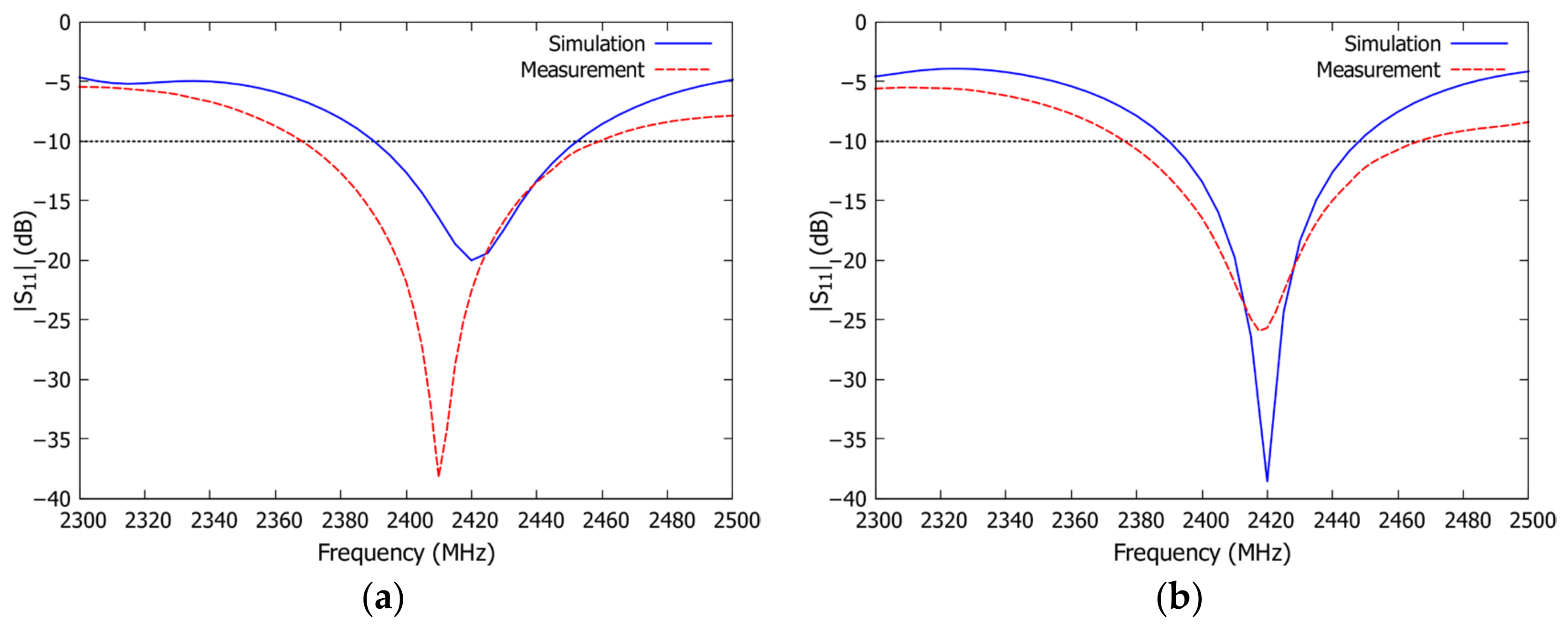
The simulation and measurement results of the S11 parameter for the designed antenna are presented in Figure 10. Figure 10a shows the results for the first state of the switching system energizing Antenna-L. In this state, the simulated resonant frequency is 2420 MHz while the measured frequency is 2410 MHz. Figure 10b presents the results for the second state of the switching system for Antenna-R. For this state, the simulated resonant frequency is 2420 MHz again and the measured frequency is 2418 MHz. These results demonstrate that the simulated and measured S11 parameters of the proposed antenna system are in good agreement. The slight discrepancies between the simulated and measured reflection coefficients can be attributed to several practical factors. First, fabrication tolerances, such as minor variations in the dielectric constant of the FR4 substrate and dimension inaccuracies during the etching process, can cause slight frequency shifts. Second, the manual soldering of the SMA connector, PIN diodes, and biasing resistors introduces parasitic inductances and capacitances that cannot be fully covered in the ideal simulation environment. Furthermore, the presence of the DC biasing wires in the near-field region and the fact that the measurements were conducted in a standard laboratory environment rather than an anechoic chamber may introduce minor environmental reflections. It is also shown that the measured −10 dB impedance bandwidth values are approximately 3.68% and 3.66% for Antenna-L and Antenna-R, respectively. Additionally, the MCU-controlled switching system successfully routes the signal to the intended antenna while maintaining stable resonant frequencies.
Figure 10.
Simulated and measured S11 parameters of the proposed antenna system for the switching states of (a) Antenna-L and (b) Antenna-R.
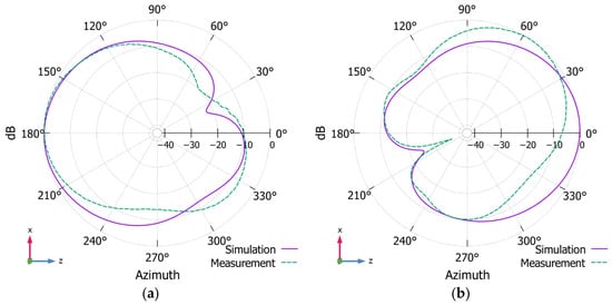
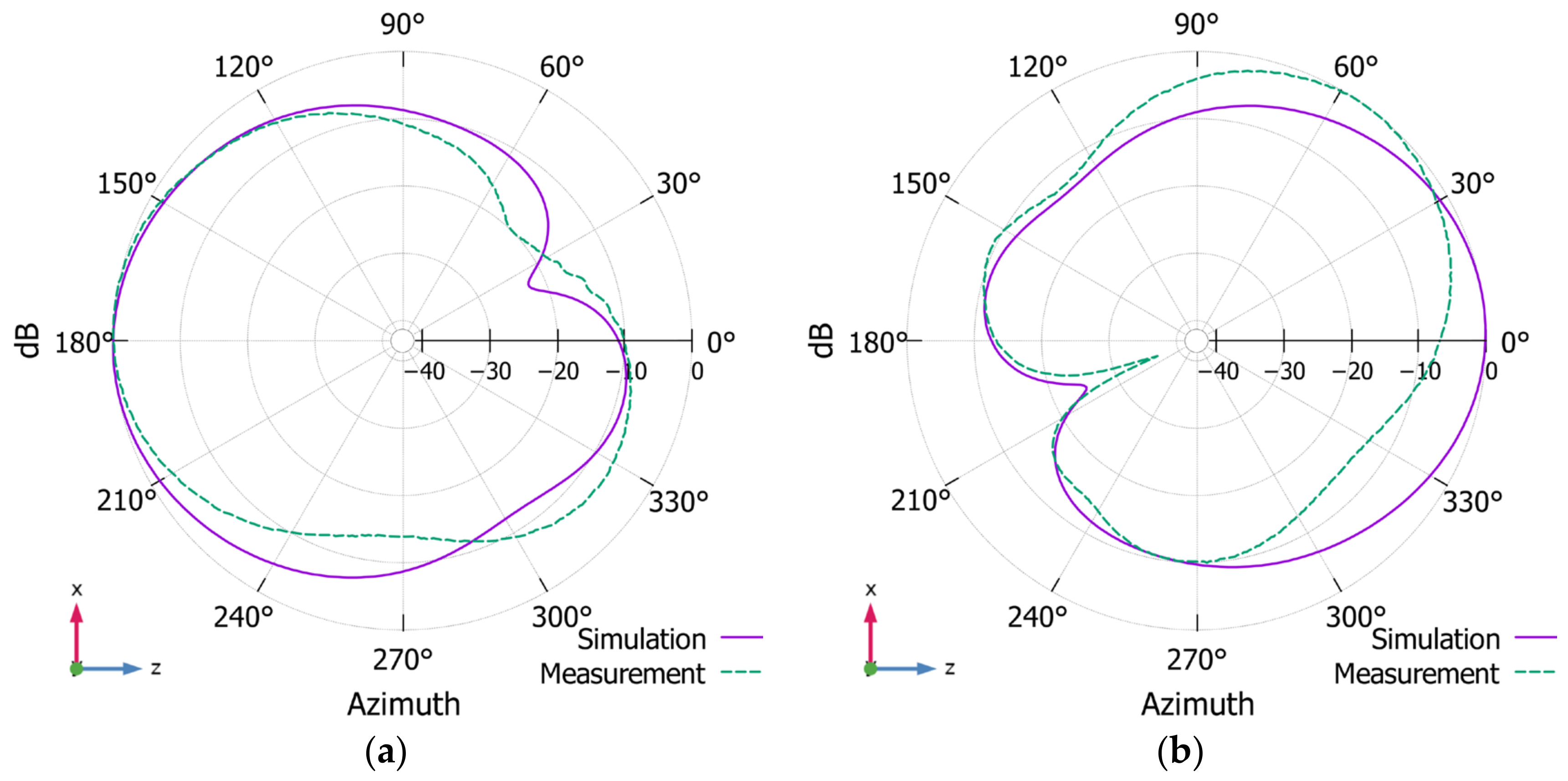
Figure 11 presents the simulated and measured normalized radiation patterns of the proposed antenna system in the azimuth plane. Figure 11a and Figure 11b illustrate the patterns when Antenna-L and Antenna-R are activated, respectively. As depicted in the polar plots, the measured results demonstrate a good agreement with the simulated data. The slight discrepancies between the simulations and measurements can be primarily attributed to fabrication tolerances and measurement setup imperfections.
Figure 11.
Simulated and measured normalized radiation patterns of the proposed antenna system for the switching states of (a) Antenna-L and (b) Antenna-R.
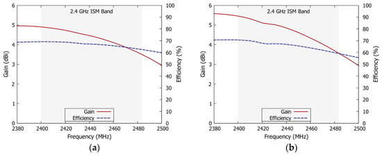
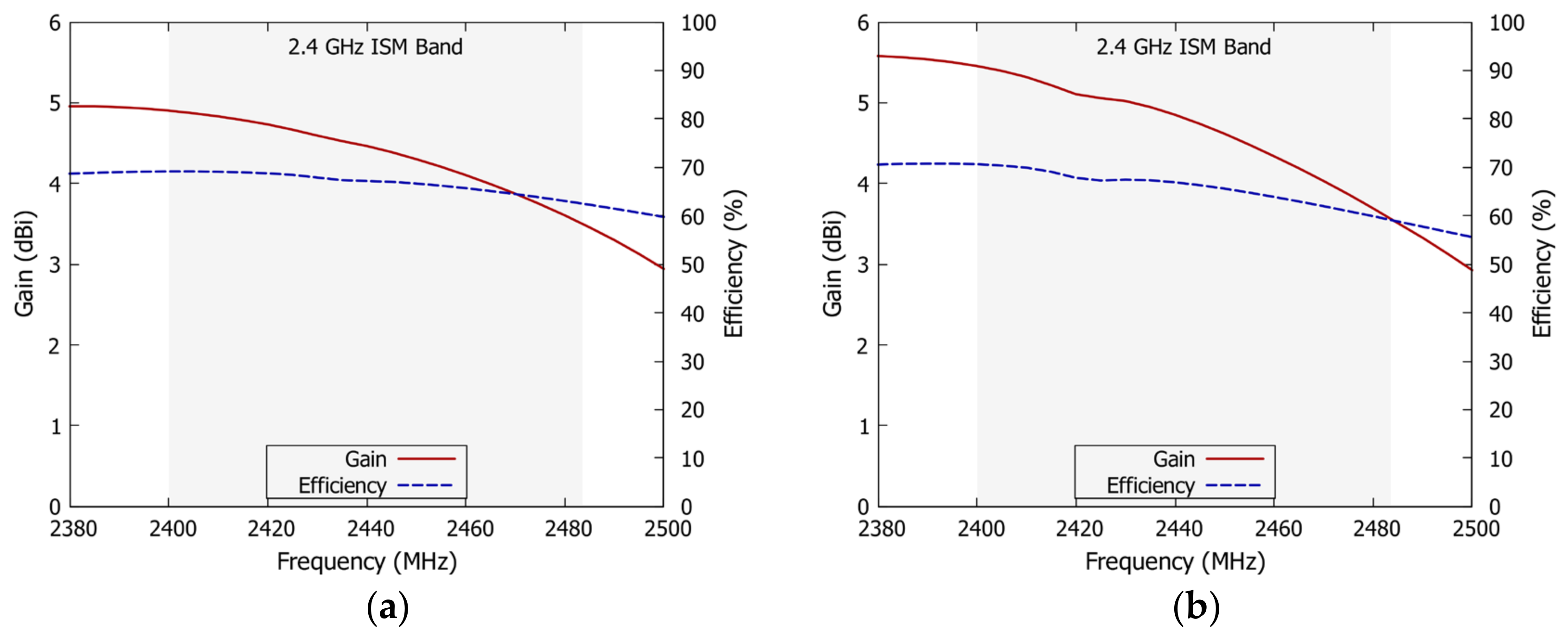
Figure 12 presents the frequency-dependent gain and radiation efficiency plots of the proposed antenna system. Figure 12a and Figure 12b illustrate the performance metrics when Antenna-L and Antenna-R are activated, respectively. As depicted in the plots, the system exhibits stable gain and efficiency levels in both operational states, especially within the 2.4 GHz ISM band highlighted in gray. In this targeted band, the radiation efficiency is observed to be between 60% and 70%. Although this efficiency level is relatively lower than that of conventional passive antennas, it is an expected and acceptable result due to the insertion losses introduced by the integrated PIN diode-based SPDT switching network and the associated lumped components on the FR4 substrate. Both curves demonstrate a consistent profile, ensuring reliable radiation performance around the targeted 2.4 GHz operating frequency.
Figure 12.
Gain and efficiency versus frequency plots of the proposed antenna system for the switching states of (a) Antenna-L and (b) Antenna-R.
Table 2 presents a performance comparison between the proposed antenna system and other existing back-to-back designs in the literature. For a comprehensive comparison, the peak performance values are reported for each work. In terms of operating bandwidth, the proposed design offers a 3.68% bandwidth. This is wider than the structure in [5,9,19]. Furthermore, the proposed antenna achieves a peak gain of 5.6 dBi, which significantly outperforms the designs presented in [9,16,19,22]. From a structural perspective, the proposed system is compact and occupies less volume than the antennas in [4,5,14,21,22]. Additionally, it is designed on a single-layer substrate. This provides a great advantage in fabrication simplicity and cost-effectiveness compared to the multi-layer structures in [4,5,9,12,16,21]. Moreover, although the designs in [6,22] also feature a single-layer structure, they often rely on expensive substrate materials or processes, further highlighting the cost efficiency of the proposed antenna. Finally, the proposed design utilizes PIN diodes for active signal routing. While the antennas in [5,12,16] lack switching capabilities, and [14] relies on basic port switching, the PIN diode integration in this work enables practical and dynamic electronic control compared to the complex MEMS-based switching in [4,22] or the hybrid Varactor and PIN diode configuration in [21]. Overall, the proposed system provides an optimal balance of high gain, structural simplicity, and effective reconfigurability.
Table 2.
Comparison of the proposed design with back-to-back antenna designs from the literature.
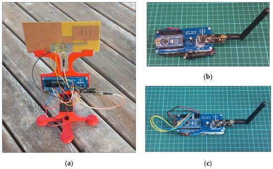
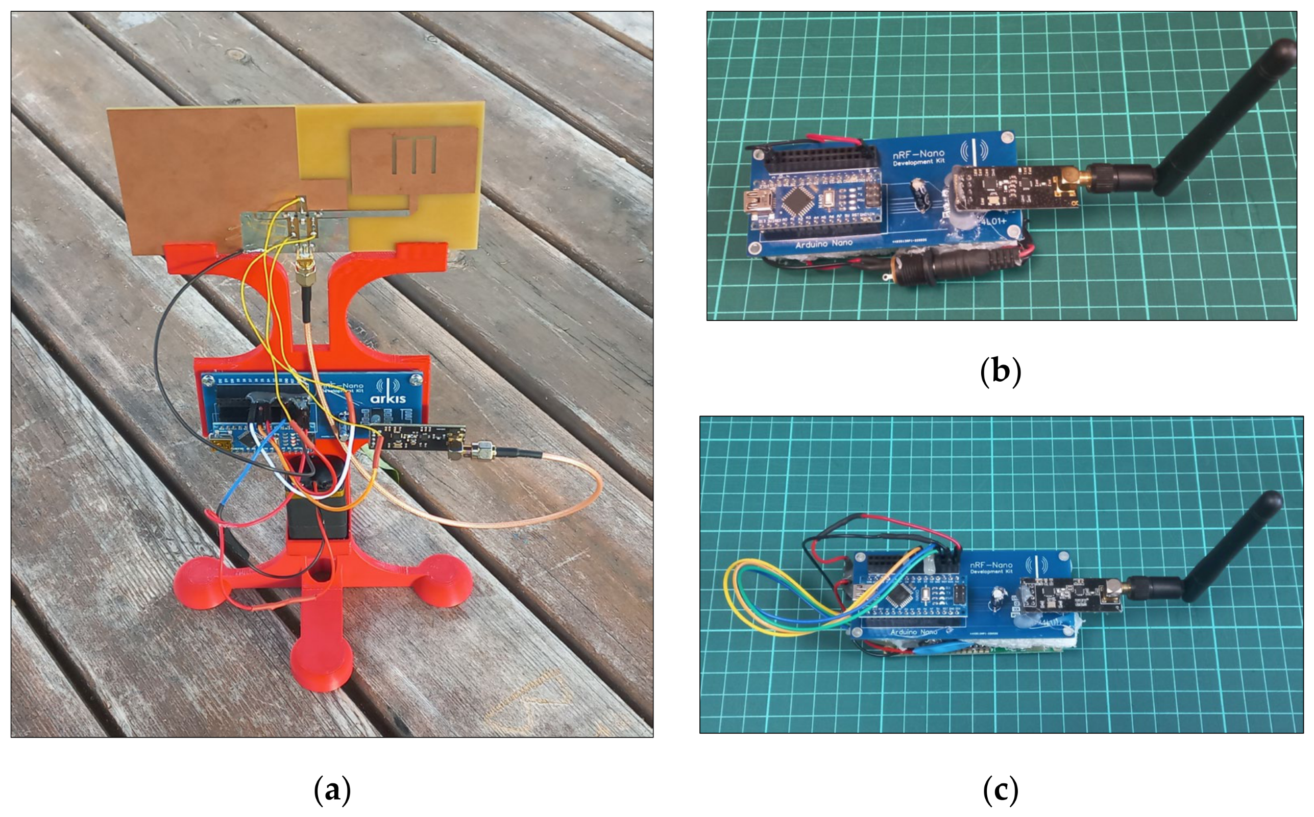
In order to validate the practical performance of the proposed switchable back-to-back E-slotted antenna, a real-world field study was conducted at the Nevsehir Haci Bektas Veli University Campus. The fabricated antenna was integrated as a key component of an active relay node for bidirectional wireless communication. Specifically, this repeater unit was constructed by combining the proposed antenna with an Arduino Nano microcontroller and an nRF24L01 (Nordic Semiconductor, Trondheim, Norway) transceiver module. The SPDT switching circuit demonstrates good energy efficiency, consuming approximately 36 mW of DC power during the active state (4.6 V, 7.8 mA). Furthermore, considering the minority carrier lifetime of the BAR64-02V PIN diodes (1.55 µs) and the digital pin execution time of the microcontroller (6.86 µs), the total switching time of the system is approximately 8.41 µs. This switching speed is sufficiently fast for practical beam switching in our wireless relay experiments. As presented in Figure 13, the central repeater unit is mounted on a custom 3D-printed pedestal. The transmitter and receiver units are equipped with standard dipole antennas, Arduino Nano microcontrollers and nRF24L01 transceivers. Custom embedded software was also developed to control the dynamic beam-switching operations in the repeater.
Figure 13.
(a) Repeater unit consisting of the proposed antenna system, nRF24L01 transceiver, and Arduino Nano on a 3D-printed pedestal stand. (b) Transmitter unit. (c) Receiver unit.
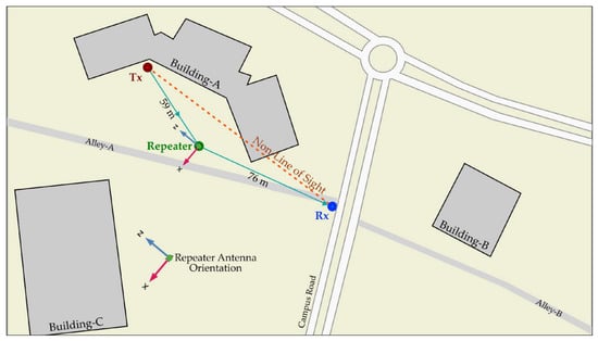
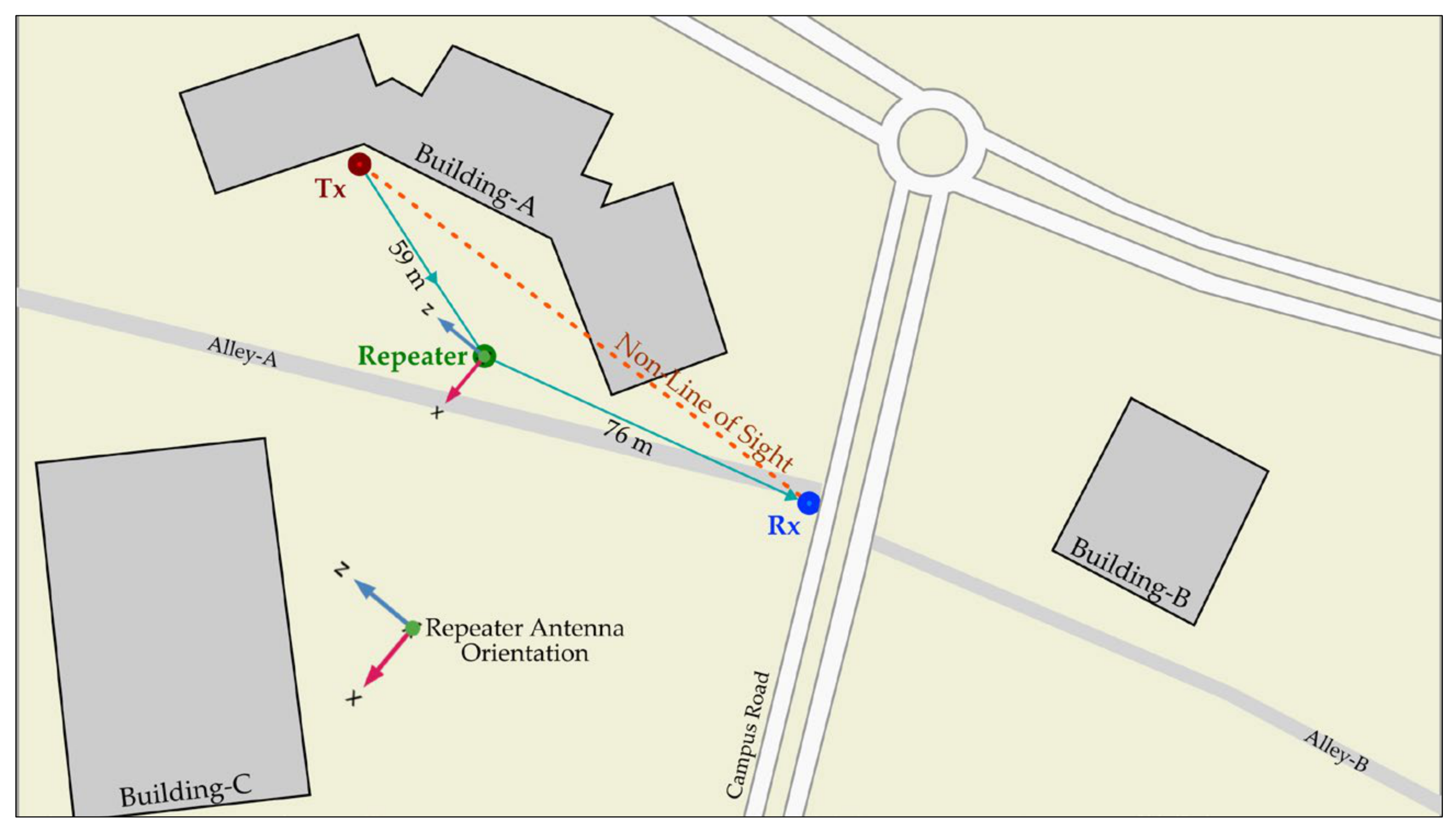
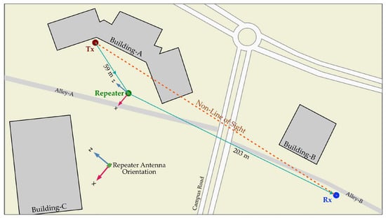
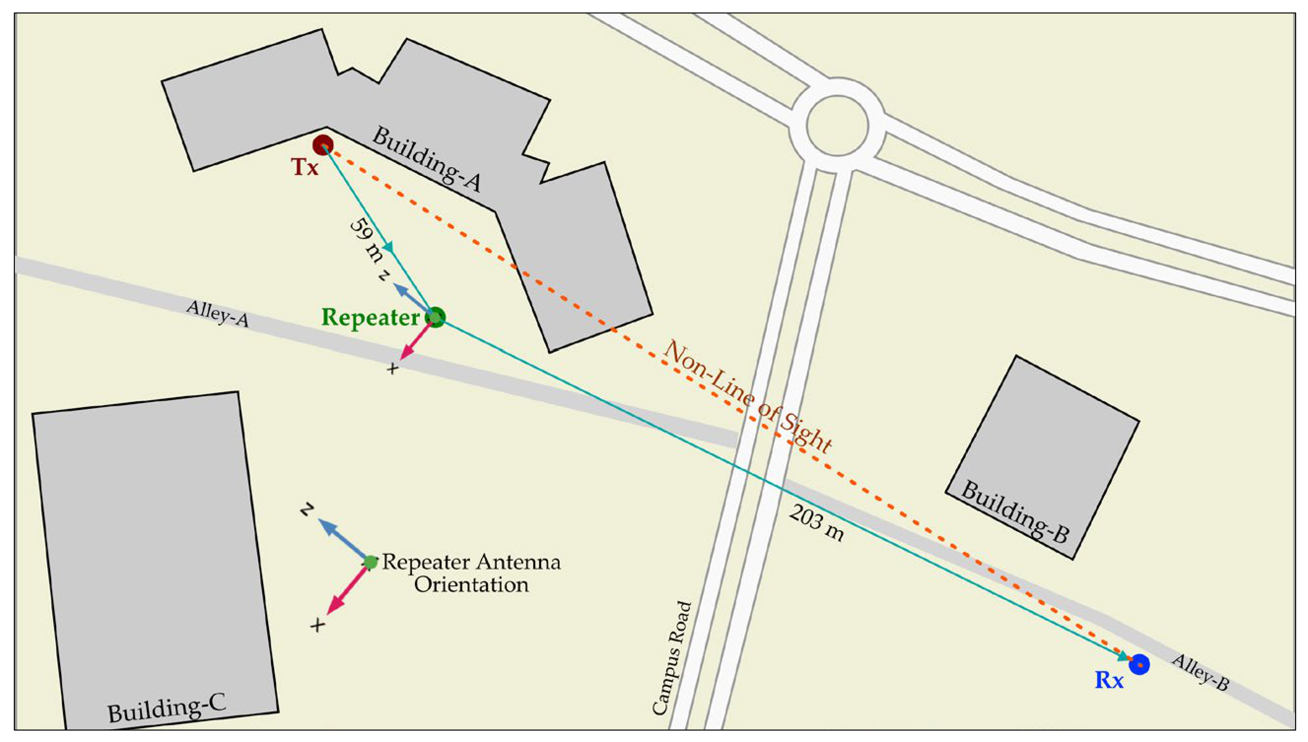
During the experiments, the receiver was deliberately placed in a severe non-line-of-sight (NLOS) environment where direct transmitter-receiver communication was physically blocked as shown in Figure 14 and Figure 15. The transmitter generates and sends a data packet containing a random payload every 50 ms. To bridge this communication gap, the proposed repeater antenna is utilized. In its idle state, the repeater directs its main beam toward the transmitter. Immediately upon receiving a packet, it switches its radiation pattern to the opposite direction and forwards the data to the receiver.
Figure 14.
Short-range field test setup employing the proposed switchable antenna in the repeater unit.
Figure 15.
Long-range field test setup employing the proposed switchable antenna in the repeater unit.
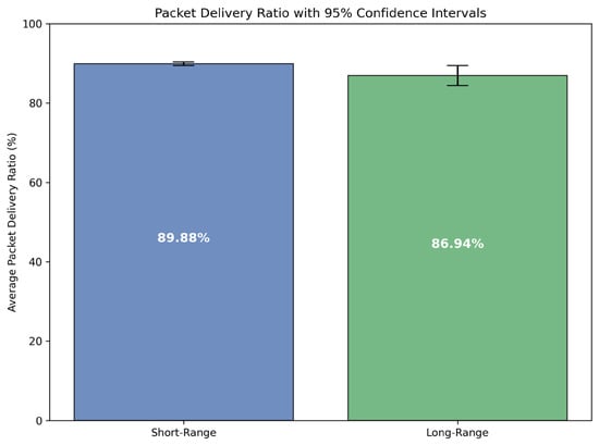
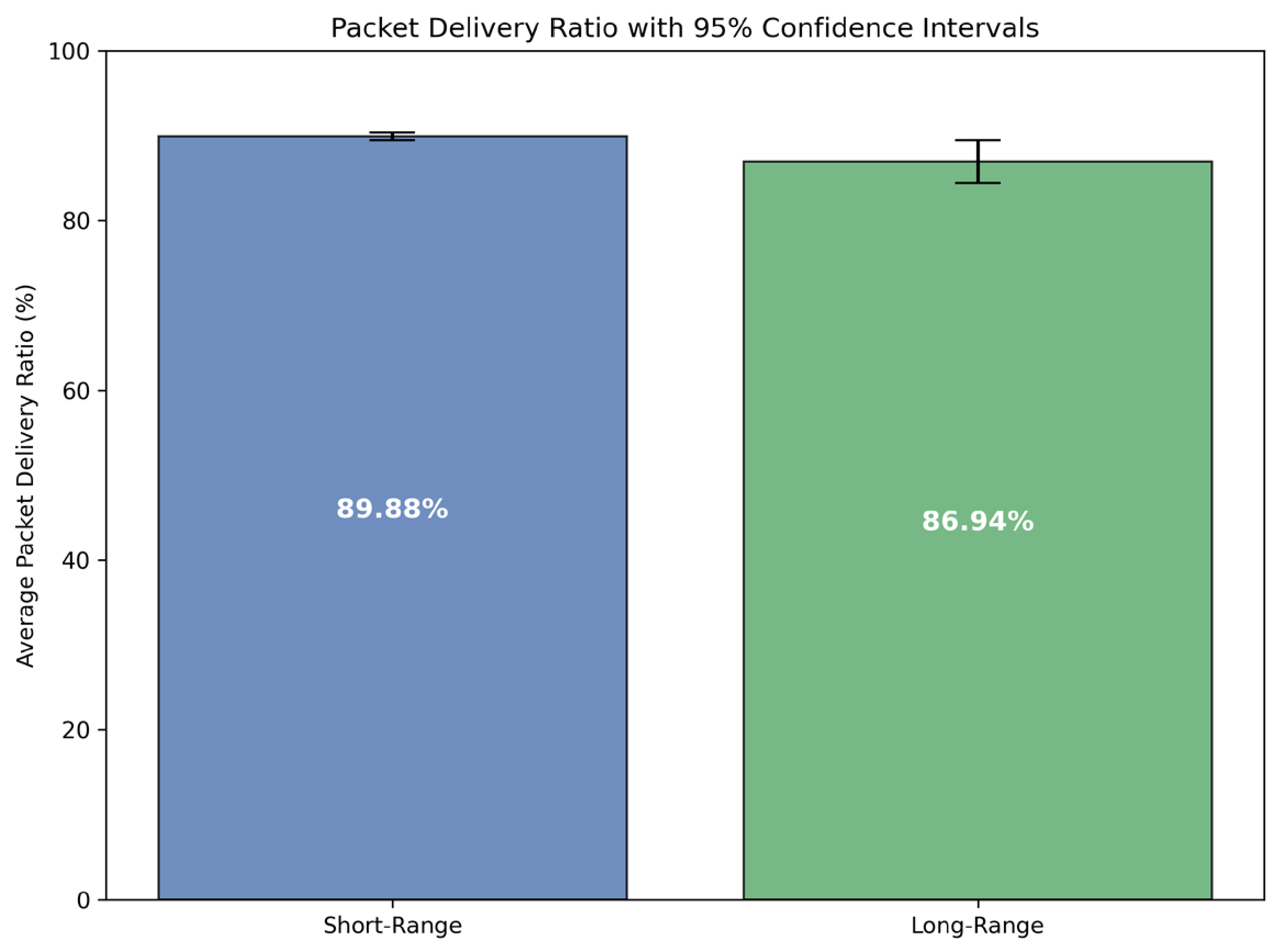
To evaluate the packet delivery ratio, two distinct testing configurations were established: a short-range setup (Figure 14) and a long-range setup (Figure 15). A total of 25,000 packets were transmitted in each scenario. The success rates were calculated for every 100-packet block, yielding 250 data groups for statistical analysis. As expected, the short-range tests outperformed the long-range tests. The short-range scenario achieved an average packet delivery success rate of 89.88% with a low standard deviation of 3.81. Similarly, the long-range scenario maintained robust performance, yielding an average success rate of 86.94% with a standard deviation of 20.20. These empirical results successfully demonstrate that the proposed switchable antenna system is a reliable and easily implementable solution for overcoming severe NLOS communication challenges. A detailed statistical analysis was conducted to evaluate the packet delivery ratios. The short-range scenario achieved an average success rate of 89.88% with a 95% confidence interval of [89.41%, 90.35%]. The long-range scenario yielded an average success rate of 86.94% with a 95% confidence interval of [84.44%, 89.44%].
The long-range setup exhibited a higher standard deviation (20.20) compared to the short-range setup (3.81). This significant variability is attributed to dynamic environmental factors in the extended physical space. Specifically, an active campus road intersected the long-range communication path. Passing vehicles caused temporary but severe blockages during the measurement periods. Furthermore, the long-range environment encompassed a higher density of trees and landscaping elements. These physical obstacles introduced dynamic multipath fading, leading to sudden drops in the packet delivery ratio. Figure 16 illustrates the mean packet delivery ratios for both setups, including error bars that represent the 95% confidence intervals. Despite these harsh environmental conditions, the system maintained a robust average performance.
Figure 16.
Average packet delivery ratios with 95% confidence intervals for both test scenarios.
4. Discussion
The results indicate that the proposed switched back-to-back E-slotted antenna functions effectively for bidirectional wireless relay applications. The measured resonant frequencies of 2410 MHz and 2418 MHz are reasonably close to the simulated target of 2420 MHz, with minor differences likely arising from fabrication tolerances and measurement setup imperfections. Furthermore, the measured radiation patterns align closely with the simulations, suggesting that the PIN diode switching circuit correctly directs the signal to the intended side. The antenna achieves a 3.68% measured bandwidth and a 5.6 dBi simulated gain, which compare favorably with several similar designs in the literature. A primary advantage of this design is its structural simplicity; unlike systems relying on multiple layers, utilizing a single-layer FR4 substrate helps keep manufacturing costs low while maintaining adequate performance.
Real-world field tests further support the practical applicability of the antenna. When evaluated as a wireless repeater in a severe non-line-of-sight (NLOS) environment, the system achieved average packet delivery ratios of 89.88% for the short-range and 86.94% for the long-range scenarios. As expected, the short-range results demonstrated higher stability with a lower standard deviation, whereas the variability at long range is likely influenced by weaker signal strength and environmental noise. These findings confirm that the system can reliably bridge communication gaps in such settings. A notable limitation of this work is the measured impedance bandwidth of 3.68%. While this is sufficient for the targeted 2.4 GHz ISM band, it is inherently narrow. To overcome this limitation, several bandwidth enhancement techniques can be considered in future designs. For example, integrating Defected Ground Structures (DGS), parasitic elements, or multilayer parasitic patches can effectively widen the operating bandwidth. Alternatively, the proposed structure can be modified to support dual-band or multi-band operations. This approach would significantly increase the adaptability of the system for different wireless communication standards. Alongside these structural improvements, broader field trials across diverse environments will be conducted to further observe the overall robustness of the system.
5. Conclusions
In conclusion, a switchable back-to-back E-slotted antenna has been successfully designed, fabricated, and tested for 2.4 GHz ISM band bidirectional wireless relay applications. By integrating opposite-facing radiating patches with a PIN diode switching circuit on a single-layer FR4 substrate, the system provides dynamic beam routing combined with structural simplicity. The antenna demonstrates reliable impedance matching, consistent radiation profiles, and relatively high gain performance in both operational states. Real-world empirical tests proved its effectiveness as an active relay node, capable of overcoming NLOS signal obstructions with high packet delivery rates. Ultimately, this study offers a cost-effective, easily implementable, and reliable hardware solution for extending the coverage and efficiency of modern wireless communication networks.
Author Contributions
Conceptualization, S.B. and A.M.C.; methodology, S.B.; software, S.B.; validation, S.B. and A.M.C.; formal analysis, S.B.; investigation, A.M.C.; resources, A.M.C.; data curation, S.B.; writing—original draft preparation, S.B. and A.M.C.; writing—review and editing, S.B.; visualization, S.B. and A.M.C.; supervision, S.B.; project administration, S.B.; funding acquisition, S.B. All authors have read and agreed to the published version of the manuscript.
Funding
This research received no external funding.
Data Availability Statement
The original contributions presented in this study are included in the article. Further inquiries can be directed to the corresponding author.
Conflicts of Interest
The authors declare no conflicts of interest.
References
- Iwasaki, H. A back-to-back rectangular-patch antenna fed by a CPW. IEEE Trans. Antennas Propag. 1998, 46, 1527–1530. [Google Scholar] [CrossRef] [Scilit]
- Hu, C.-C.; Jou, C.F.; Wu, J.-J.; Peng, S.T. A back-to-back dual-beam active microstrip leaky-wave antenna array with mode-switching capability. Microw. Opt. Technol. Lett. 2000, 24, 195–197. [Google Scholar] [CrossRef] [Scilit]
- Vian, J.; Popovic, Z. A transmit/receive active antenna with fast low-power optical switching. IEEE Trans. Microw. Theory Tech. 2000, 48, 2686–2691. [Google Scholar] [CrossRef] [Scilit]
- Grau, A.; Romeu, J.; Jofre, L.; De Flaviis, F. Back-to-back high-isolation iso-frequency repeater antenna using MEMS-Reconfigurable-Parasitics. In Proceedings of the IEEE Antennas and Propagation Society International Symposium; IEEE: New York, NY, USA, 2007; pp. 497–500. [Google Scholar]
- Kang, H.; Lim, S. High isolation transmitter and receiver antennas using high-impedance surfaces for repeater applications. J. Electromagn. Waves Appl. 2013, 27, 2281–2287. [Google Scholar] [CrossRef] [Scilit]
- Sharma, S.K.; Fideles, F.; Kalikond, A. Planar Yagi-UDA Antenna with Reconfigurable Radiation Patterns. Microw. Opt. Technol. Lett. 2013, 55, 2946–2952. [Google Scholar] [CrossRef] [Scilit]
- Sharma, S.K.; Fideles, F.; Kalikonda, A. Radiation pattern reconfigurable planar Yagi-Uda antenna. In Proceedings of the IEEE Antennas and Propagation Society International Symposium (APSURSI), Orlando, FL, USA, 7–13 July 2013; IEEE: New York, NY, USA, 2013; pp. 190–191. [Google Scholar]
- Komaki, K.; Iwasaki, H. Back to back patch antenna operated orthogonal polarization for repeater use. In Proceedings of the International Symposium on Antennas and Propagation (ISAP); IEEE: New York, NY, USA, 2015; pp. 1–2. [Google Scholar]
- Yang, K.; Bao, X.; Ammann, M.J. A back-to-back beam switching microstrip patch antenna. In Proceedings of the Loughborough Antennas & Propagation Conference (LAPC); IEEE: New York, NY, USA, 2015; pp. 1–4. [Google Scholar]
- Yang, K.; Bao, X.; McEvoy, P.; Ammann, M.J. Pattern reconfigurable back-to-back microstrip patch antenna. IET Microw. Antennas Propag. 2016, 10, 1390–1394. [Google Scholar] [CrossRef] [Scilit]
- Hou, Y.; Li, Y.; Chang, L.; Zhang, Z.; Feng, Z. Bidirectional same-sense circularly polarized antenna using slot-coupled back-to-back patches. Microw. Opt. Technol. Lett. 2017, 59, 645–648. [Google Scholar] [CrossRef] [Scilit]
- Kashanianfard, M.; Sarabandi, K. Directional Full-Duplex RF Booster for 2450 MHz ISM Band. IEEE Trans. Antennas Propag. 2017, 65, 134–141. [Google Scholar] [CrossRef] [Scilit]
- Das, G.; Sharma, A.; Gangwar, R.K.; Sharawi, M.S. Compact back-to-back DRA-based four-port MIMO antenna system with bi-directional diversity. Electron. Lett. 2018, 54, 884–886. [Google Scholar] [CrossRef] [Scilit]
- Jo, H.-W.; Kim, G.; Yoo, J.-S.; Yu, J.-W. Back-To-Back Magnetic Dipole Antennas with Pattern Reconfigurability. In Proceedings of the IEEE International Symposium on Antennas and Propagation & USNC/URSI National Radio Science Meeting; IEEE: New York, NY, USA, 2018; pp. 979–980. [Google Scholar]
- Singh, G.; Kanaujia, B.K.; Pandey, V.K.; Gangwar, D.; Kumar, S. Pattern and frequency reconfigurable antenna with diode loaded ELC resonator. Int. J. Microw. Wirel. Technol. 2020, 12, 163–175. [Google Scholar] [CrossRef] [Scilit]
- Zhang, P.; Yi, H.; Liu, H.; Yang, H.; Zhou, G.; Li, L. Back-to-Back Microstrip Antenna Design for Broadband Wide-Angle RF Energy Harvesting and Dedicated Wireless Power Transfer. IEEE Access 2020, 8, 126868–126875. [Google Scholar] [CrossRef] [Scilit]
- Eissa, M.; Sukhanov, D. Enhancing performance in a LOS MIMO communication using a passive repeater. J. Phys. Conf. Ser. 2021, 2140, 012013. [Google Scholar] [CrossRef] [Scilit]
- Megalou, S.; Dimitriou, A.G.; Tzitzis, A.; Yioultsis, T.V. Design and Fabrication of a Compact, Low-Cost UHF-RFID Repeater, Exploiting Circular Cross-Polarization. IEEE J. Radio Freq. Identif. 2021, 5, 64–74. [Google Scholar] [CrossRef] [Scilit]
- Yan, Y.-D.; Jiao, Y.-C.; Zhang, C. Pattern and polarization reconfigurable circularly polarized antenna based on two pairs of planar complementary dipoles. Microw. Opt. Technol. Lett. 2021, 63, 876–882. [Google Scholar] [CrossRef] [Scilit]
- Zhang, W.; Li, Y.; Wei, K.; Zhang, Z. Dual-Band Decoupling for Two Back-to-Back PIFAs. IEEE Trans. Antennas Propag. 2023, 71, 2802–2807. [Google Scholar] [CrossRef] [Scilit]
- Panda, P.; Mathur, R.; Mahajan, A. Electronically Controllable Varactor Loaded Beam Switchable 4-Element Array Antenna for Sub-6 GHz Application. IEEE Access 2025, 13, 46042–46053. [Google Scholar] [CrossRef] [Scilit]
- Cheng, S.; Rantakari, P.; Malmqvist, R.; Samuelsson, C.; Vaha-Heikkila, T.; Rydberg, A.; Varis, J. Switched Beam Antenna Based on RF MEMS SPDT Switch on Quartz Substrate. In Proceedings of the IEEE Antennas and Wireless Propagation Letters; IEEE: New York, NY, USA, 2009. [Google Scholar]
- Lamultree, S.; Thanamalapong, W.; Dentri, S.; Phongcharoenpanich, C. Tri-Band Bidirectional Antenna for 2.4/5 GHz WLAN and Ku-Band Applications. Appl. Sci. 2022, 12, 5817. [Google Scholar] [CrossRef] [Scilit]
- Nkimbeng, C.H.S.; Wang, H.; Park, Y.B.; Park, I. Wideband Circularly Polarized Metasurface-Integrated Dipole Antenna for Bidirectional Applications. Int. J. Antennas Propag. 2025, 2025, 2169177. [Google Scholar] [CrossRef] [Scilit]
- Gad, M.M.; Sallam, M.O.; Ameen, A.M.; Bakr, M.H.; Soliman, E.A. Ultra-Thin Compact Bidirectional S-Slot Antenna for 5G Communications. Telecom 2026, 7, 46. [Google Scholar] [CrossRef] [Scilit]
- Root, D.E.; Verspecht, J.; Horn, J.; Marcu, M. X-Parameters: Characterization, Modeling, and Design of Nonlinear RF and Microwave Components; Cambridge University Press: Cambridge, MA, USA, 2013. [Google Scholar]
- Kobrinsky, M.J.; Chakravarty, S.; Jiao, D.; Harmes, M.C.; List, S.; Mazumder, M. Experimental validation of crosstalk simulations for on-chip interconnects using S-parameters. IEEE Trans. Adv. Packag. 2005, 28, 57–62. [Google Scholar] [CrossRef]

Disclaimer/Publisher’s Note: The statements, opinions and data contained in all publications are solely those of the individual author(s) and contributor(s) and not of MDPI and/or the editor(s). MDPI and/or the editor(s) disclaim responsibility for any injury to people or property resulting from any ideas, methods, instructions or products referred to in the content. |
© 2026 by the authors. Licensee MDPI, Basel, Switzerland. This article is an open access article distributed under the terms and conditions of the Creative Commons Attribution (CC BY) license.