


Abstract
This paper presents the design of high-performance, low-loss planar microwave filters by using an inverted shielded transmission line topology with an air gap. By suspending inverted conductive traces above a longitudinal air cavity and enclosing the propagating fields within multi-row vertical shielding via arrays, the architecture effectively mitigates the severe dielectric dissipation inherent in low-cost substrates. To demonstrate the efficacy of this design framework, two distinct planar filter components are synthesized, fabricated, and experimentally characterized: a 7th-order Stepped-Impedance Resonator (SIR) lowpass filter and a 3rd-order Parallel-Coupled Line (PCL) bandpass filter. Both implemented devices demonstrate high in-band signal integrity, achieving minimal insertion losses of 0.31 dB and 1.1 dB, respectively. Ultimately, this design approach successfully resolves the traditional trade-off between high electrical efficiency and manufacturing cost for advanced microwave filtering applications.
1. Introduction
The rapid evolution of wireless communication systems, including 5G/6G networks and Internet of Things (IoT) architectures, has imposed increasingly strict demands on microwave front-ends. The realization of high-efficiency planar microwave devices is fundamentally constrained by the inherent loss mechanisms of conventional TL structures. Underlying transmission lines (TLs) dictate both the overall efficiency and the manufacturing expense of the communication link.
While employing specialized substrates can mitigate losses, this approach significantly escalates manufacturing costs. Overcoming this fundamental bottleneck requires a departure from standard geometries in favor of alternative topologies that intrinsically reduce loss mechanisms without relying on expensive substrates.
A primary research approach involves the aggressive physical modification or removal of the host substrate to increase the proportion of the field stored in air. Techniques such as CO2 laser drilling [1], mechanical milling of air cavity waveguides [2], and the synthesis of hollow dielectric cores [3] have been employed to reduce dielectric volume and suppress energy dissipation. While these approaches achieve excellent high-frequency attenuation constant characteristics, they are mechanically intensive and often require complex post-processing steps. Furthermore, some of these modifications rely on expensive, low-loss laminate materials (e.g., Rogers RT/duroid) rather than commodity FR4, negating the primary economic motivation for planar design. Other research studies have investigated the manipulation of ground plane boundaries using slots, defects, and surface-level imperfections. Methods such as etched rectangular slots [4,5], defected ground structures (DGS) [6], or capacitively loaded TLs and resonators [7,8,9] tune the line’s local inductance and capacitance to achieve desired characteristics. Although effective for specialized frequency tuning, these ground plane modifications could introduce significant backward radiation and common-mode leakage, which degrades the electromagnetic integrity of the interconnect. Similarly, surface-level enhancements such as plasma treatment or mechanical polishing [10,11] aim to mitigate conductor roughness, yet they necessitate complex chemical or mechanical re-flow techniques that significantly increase fabrication complexity while offering limited performance returns at frequencies below 10 GHz.
A more robust method for field containment utilizes active shielding through vertical via-fencing and electromagnetic bandgap (EBG) structures. Multi-layer strip line configurations [12] and optimized via-transition geometries [13] demonstrate the utility of dense ground via cages in restricting field divergence. Taking this further, Inverted Microstrip Gap Waveguide (IMGW) and EBG-based topologies [14,15] provide field containment by synthesizing an artificial magnetic conductor surface that suppresses wave leakage into the substrate. However, these solutions are hampered by their rigid mechanical requirements, often requiring precision-machined split-block assemblies, bulky packaging screws, and consistent air gap heights that resist miniaturization to standard sub-6 GHz microwave scales.
Finally, researchers have also sought to increase the relative effective permittivity through periodic reactive loading or corrugation [16,17,18]. By cascading stepped-impedance elements or surface-grooved resonators, designers can achieve substantial footprint reduction and frequency selectivity. Nevertheless, these periodic perturbations inevitably trigger loss and phase velocity mismatch.
Despite the proliferation of advanced wireless systems, a persistent industrial challenge lies in reconciling high-performance RF filtering with strict cost constraints. While commercial microwave components predominantly rely on expensive, low-loss specialty substrates (such as PTFE-based laminates or ceramics) to maintain high-quality factors (Q), mass-market commercial deployment demands cost-effective alternatives such as standard FR4 boards. However, conventional FR4 suffers from high-dielectric loss (tan δ ≈ 0.027) and severe signal attenuation at microwave frequencies, rendering unshielded planar implementations inadequate for low-loss filter realization. This creates a critical industrial bottleneck: achieving high-frequency, low-loss performance without resorting to expensive specialized materials.
To bridge the critical gap between high-performance microwave requirements and the strict economic constraints of mass-market commercial production, the Air-Void Inverted Shielded (AVIS) architecture was purposefully designed. Rather than relying on expensive, specialty microwave substrates to mitigate high-frequency losses, this structure aims to unlock the full potential of standard, low-cost multi-layer FR4 technology by engineering a solution that eliminates dielectric dissipation without sacrificing manufacturing scalability. By embedding an inverted conductive strip above a longitudinal air cavity and enclosing the propagating fields within a multi-row vertical shielding via array, the AVIS approach effectively confines high-intensity electric fields within a lossless medium, thereby mitigating bulk dielectric dissipation. This structural improvement offers a robust solution, eliminating the need for premium, high-cost laminates or complex, non-planar micro-machining typically required to achieve high performance. The efficacy of this framework is validated through the synthesis and fabrication of a stepped-impedance lowpass filter and parallel-coupled bandpass filter on a standard FR4 substrate.
In contrast to these prior methodologies, the proposed AVIS topology addresses their collective limitations through a structurally decoupled design. While earlier shielding arrays [12] and multi-layer DGS layouts [6] remain embedded in lossy dielectrics, the AVIS line eliminates bulk substrate dissipation by routing an evacuated air cavity beneath the active trace. Unlike hollow waveguide implementations [2,3] or surface-treated lines [10], it completely avoids expensive microwave laminates, enclosed non-planar profiles, and post-fabrication chemical polishing, operating entirely within a standard, low-cost multi-layer FR4 stackup. Furthermore, unlike slotted-ground topologies [4,5,8] that suffer from severe backward radiation, or periodic slow-wave structures [16,17] that introduce strong phase velocity dispersion, the AVIS architecture maintains a solid, continuous system ground plane. While conventional suspended microstrips require bulky external metallic housings to prevent radiation, and inverted microstrip gap waveguides rely on complex, periodic electromagnetic bandgap (EBG) structures to create stopbands, the AVIS topology achieves field confinement through a simple, continuous grounded via fence. Furthermore, the fundamental novelty of this architecture lies in its strategic layer arrangement, which actively forces the majority of the field lines to propagate through a localized, low-loss air medium. This combination of an air-dielectric core and an electric wall boundary terminates the lateral electric fields with almost no perturbation of the magnetic loop trajectory, providing a high unloaded quality factor alongside a flat, quasi-dispersionless phase response.
Moreover, this work directly addresses the industrial challenges listed earlier since it provides a scalable, low-cost manufacturing pathway to achieve low-loss microwave filtering entirely within standard multi-layer FR4 technology.
Specifically, the fundamental scientific original contributions of this work are summarized as follows:
- ⚬
- A Novel Hybridized Transmission Architecture: The introduction of a structurally decoupled topology that successfully merges an inverted signal trace, a routed air cavity, and a dense via-fence cage into a single, cohesive geometry entirely within a standard multi-layer FR4 stackup.
- ⚬
- Electric Field Confinement: The demonstration of a localized electric wall boundary that strictly terminates lateral electric field lines, eliminating the severe radiation leakage and parasitic cross-coupling typically associated with standard suspended or air cavity lines without relying on dispersive Bragg resonances.
- ⚬
- Benchmark Validation on Lossy Substrates: The first rigorous design, fabrication, and empirical validation of this specific architecture applied to classical Stepped-Impedance Resonator (SIR) and Parallel-Coupled Line (PCL) filters, confirming that high-quality-factor microwave performance can be systematically extracted from inherently lossy commercial FR4.
The rest of the paper is organized as follows. Section 2 details the multi-layer FR4 stackup and the physical AVIS architecture. Section 3 presents full-wave 3D electromagnetic simulations, including a parametric analysis for the quality factor of different shielding via configurations. The validation of this framework is then demonstrated through the synthesis of two distinct planar components: Section 3 presents the design, simulation, and experimental verification of a 7th-order Stepped-Impedance Resonator (SIR) lowpass filter, while Section 4 applies the same methodology to a Parallel-Coupled Line (PCL) bandpass filter. Finally, Section 5 concludes the paper.
2. High-Q AVIS TLs: Technology and Topology Description
In this work, the proposed Air-Void Inverted Shielded (AVIS) architecture utilizes an etched air cavity with a controlled vertical air gap (t2) to house the microstrip resonators, which collectively form a suspended structure free of underlying dielectric support.
2.1. Stackup Description
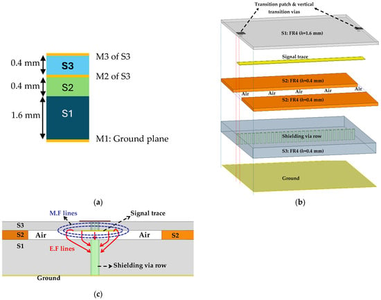
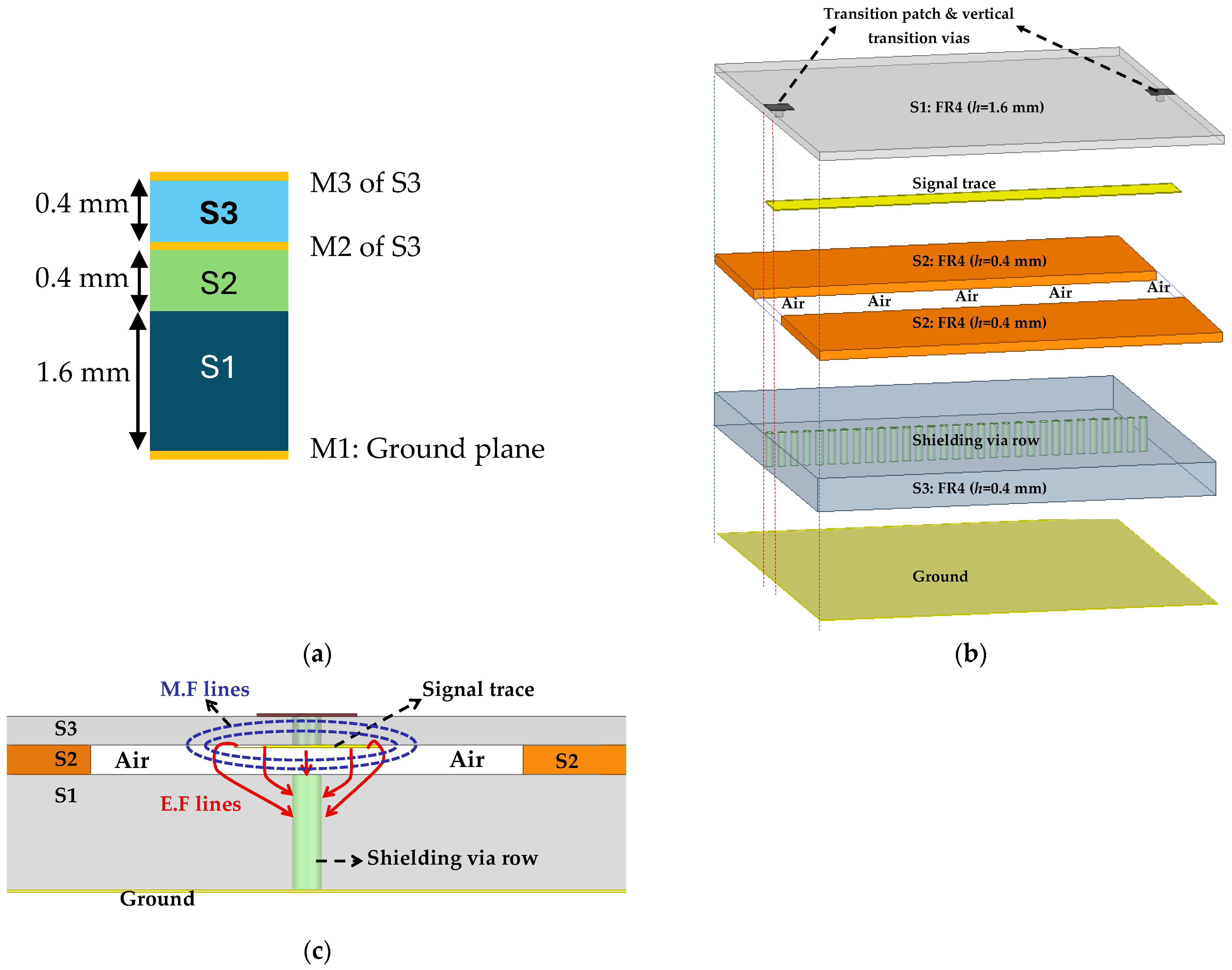
The TL architecture uses a three-layer PCB stack, as shown in Figure 1a. The layer properties are summarized in Table 1. In accordance with the manufacturer’s datasheet specifications at a reference frequency of 1 GHz, all FR4 layers are modeled with a relative permittivity of εr = 4.4 and a loss tangent of tan δ = 0.027. All the layers have a loss tangent of tan δ = 0.027, copper thickness of 35 µm, and copper bulk conductivity of σ = 5.8 × 10⁷ S/m across the considered frequency band.
Figure 1.
(a) Substrate stack used in the design, (b) 3D perspective cutaway, and (c) cross-sectional schematic view of the proposed AVIS TL topology.
Table 1.
Substrate properties and geometric profiles.
2.2. Architecture
Figure 1b,c depicts the structural configuration and cross-sectional profile of the AVIS transmission line. To fundamentally isolate the electric field lines from lossy materials, the signal strip is inverted and attached to the lower boundary of the top substrate layer (S3). Directly beneath this embedded strip, the central FR4 spacer (S2) is modified with a routed longitudinal channel, establishing an unclad air cavity. This geometry suspends the signal strip over the void, forcing the fringing electric field lines to concentrate within the low-loss air medium rather than the surrounding FR4. Furthermore, lateral electric field leakage is suppressed by an arrangement of vertical shielding vias anchored in the base substrate (S1). This bed of nails metallic wall intercepts the electric field lines, tightly confining the guided wave and minimizing dielectric attenuation, while keeping the relative effective permittivity at an acceptable value. The magnetic field experiences negligible perturbation since the signal strip and ground plane configurations mirror those of classical microstrip lines. This inductive stability is quantitatively verified through distributed parameter extraction in Section 2.3.1. For measurement purposes, standard RF interfacing is achieved via localized copper patches on the top surface of S3. The RF signal is vertically transitioned to the hidden signal strip through a plated via penetrating the 0.4 mm profile of the upper substrate.
2.3. Parameter Extraction and Transmission Line Design
2.3.1. Parametric Study and Performance Evaluation
To evaluate the electromagnetic propagation characteristics of the AVIS topology, EM simulations were carried out using Ansys HFSS to extract the two-port S-parameters, specifically the transmission (S21) and reflection (S11) coefficients. The physical length of the simulated model was fixed at 64 mm. In numerical full-wave simulations, selecting an adequate physical line length is essential to decouple port discontinuity effects from intrinsic propagation characteristics. Because the wave ports in the 3D simulation are assigned directly to the cross-sectional boundaries of the uniform AVIS transmission line, no external microstrip feed transitions are present, meaning port de-embedding is not required. However, localized evanescent modes are inevitably excited at the interface between the wave ports and the discrete via-shielded air cavity. Setting the line length to 64 mm (≈0.35 − 0.4λg at 1 GHz) provides sufficient physical distance for these higher-order modes to attenuate fully prior to the measurement reference planes. From the extracted S-parameters, the [ABCD] matrix was calculated for the two-port AVIS TL. The A, B, C, and D represent the complex elements of the 2 × 2 ABCD (chain) transmission matrix, where A is the reverse voltage ratio (dimensionless), B is the transfer impedance expressed in ohms (Ω), C is the transfer admittance expressed in siemens (S), and D is the forward current ratio (dimensionless).
The characteristic impedance (Zc in Ohm) of the TL and the complex propagation constant (γ in m−1) were then analytically determined as:
with:
with the attenuation constant (α in Np/m) and the phase constant (β in rad/m), used to calculate the unloaded quality factor Q (dimensionless) as:
γ = α + jβ,
When extracting the complex propagation constant (γ) from the transmission matrix, the mathematical branch ambiguity inherent in the cosh−1(A) function is resolved by enforcing strict phase continuity [7]. A standard phase-unwrapping procedure is applied across the frequency sweep to ensure that the extracted phase constant (β) increases monotonically, preventing non-physical 2π phase jumps.
To establish a versatile baseline that intrinsically balances dielectric containment with metallic losses, the topology was systematically evaluated across a comprehensive parametric matrix. The full-wave simulations sweep the total number of shielding via rows (N = 1, 3, 5, 7), specific via diameters (dv = 0.2, 0.4, 0.8 mm), and center-to-center pitch separations (Xv = 0.4, 0.6, 0.8, 1.6 mm). For each variation, the strip width was adjusted to maintain a characteristic impedance of approximately 50 Ω. The primary objective of this full-wave analysis was to map the fundamental capabilities and structural limits of the AVIS technology.
A 3D electromagnetic modeling and full-wave analysis of the proposed AVIS structures were conducted using Ansys HFSS. The feed lines were excited using standard 50-Ω wave ports. The computational domain was truncated using absorbing radiation boundaries positioned at a distance of quarter-wavelength from the edges of the structure to prevent artificial wave reflections. The metallic traces, ground plane, and shielding via walls were modeled with finite conductivity corresponding to standard copper (σ = 5.8 × 10⁷ S/m). To guarantee high-fidelity resolution of the electromagnetic fields—particularly across the critical interfaces of the evacuated air cavity and the dense via array—an adaptive tetrahedral meshing algorithm was employed. The mesh convergence criterion was strictly set to a maximum ΔS of 0.02, ensuring rigorous numerical stability and accurate extraction of the unloaded quality factors. A minimum of two converged passes criterion was set to ensure accurate results.
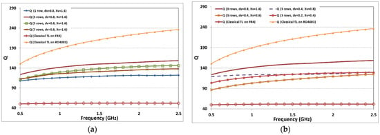
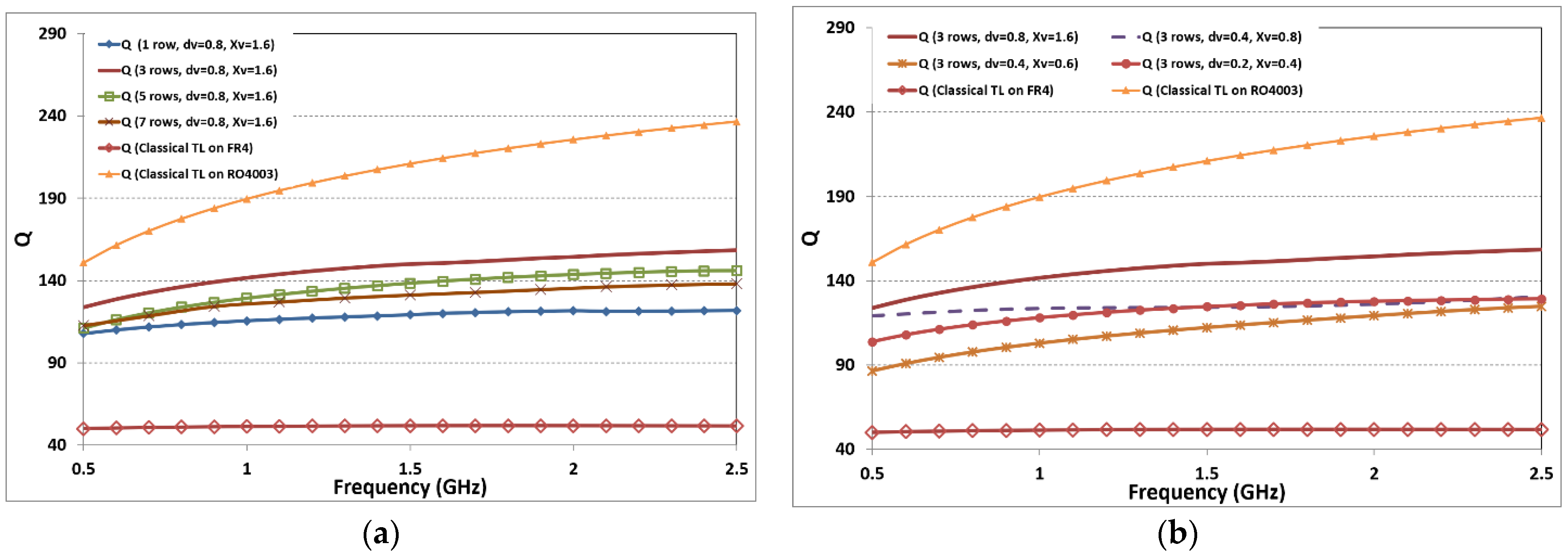
The plot in Figure 2 shows the Q-factor for all variations of rows, dv, and Xv. While a conventional unshielded microstrip line printed on solid FR4 limits the Q-factor to approximately 50 across the band due to severe dielectric dissipation, capturing the wave within the AVIS channel elevates the Q-factor significantly, ranging from 85 to 160, depending on the structural dimensions. The parametric extraction reveals a critical physical boundary governing the technology: ultra-dense shielding arrays—such as those utilizing narrow 0.2 mm vias compressed at a 0.4 mm pitch—effectively halt lateral electric field leakage but induce a severe metallic penalty.
Figure 2.
Simulated unloaded quality factor for all variations: (a) row variation, and (b) separation variation.
To analytically substantiate the simulation observations regarding via-induced ohmic losses, the total series resistance per unit length (R′wall) of the shielding via array can be modeled by considering the skin-effect current distribution over the cylindrical via walls. For a via array of pitch Xv, diameter dv, and height h, the number of vias per unit length is N = 1/Xv. At microwave frequencies, high-frequency return currents flowing through the shielding structure are strictly confined to the metallic skin depth ( in m). The equivalent AC resistance contributed by a single plated via in Ohm is expressed as:
where Rs is the surface resistivity of the copper plating in Ohm. When ultra-dense configurations are utilized (e.g., dv = 0.2 mm at a 0.4 mm pitch), reducing the individual via diameter dv linearly decreases the localized current-carrying surface area. Furthermore, the tight spatial proximity intensifies current crowding and proximity-effect resistance around the narrow via barrels. Despite the increased number of parallel conduction paths, the elevated current density around the narrow via perimeters spikes the total ohmic loss (Ploss = I2R′wall). This physical mechanism explains the suppressed unloaded quality factor observed in extreme via density regimes.
On the other hand, the simulated Q-factor for the 3-row AVIS TL having (dv, Xv) = (0.8, 1.6) mm, offers the maximum value of 124 at 0.5 GHz, maintaining an increasing trajectory up to 160 at 2.5 GHz. It is worth noting that the frequency range investigated in this work (0.5–2.5 GHz) focuses specifically on the traditional sub-6 GHz microwave spectrum. While ultra-high-frequency millimeter-wave (mmWave) and terahertz (THz) domains demand specialized micro-machining and substrate technologies, this work targets the high-volume microwave band to address the pressing industrial need for low-cost, high-performance FR4 solutions.
This specific configuration—utilizing 3 rows with dv = 0.8 mm and Xv = 1.6 mm—was systematically selected as the optimal baseline because it successfully maximizes the unloaded Q-factor (reaching up to 160) while avoiding the severe ohmic skin depth penalty associated with ultra-dense, narrow via arrays. This TL is going to be used later at the input and output ports of the designed filters.
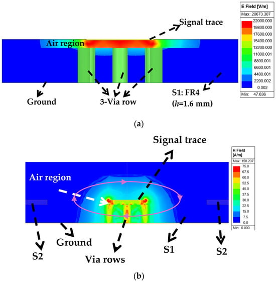
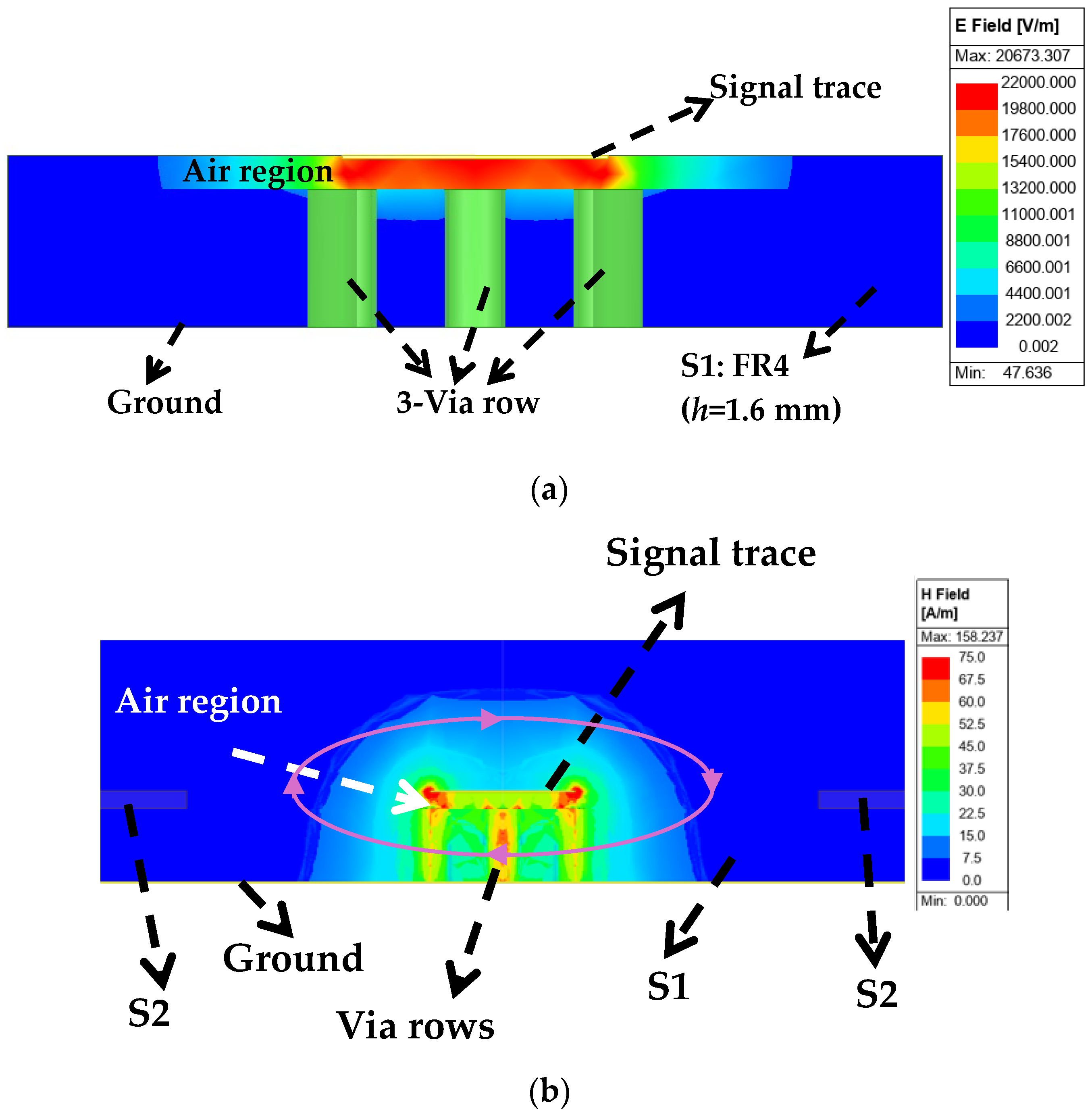
To visually validate the underlying physics driving this optimized performance, the cross-sectional electric and magnetic field magnitude distributions for the three-row architecture (dv = 0.8 mm, Xv = 1.6 mm) is presented in Figure 3. As demonstrated by the normalized color scale, the dense, high-intensity electric fields—indicated by the red and orange regions—are strictly confined directly beneath the inverted signal strip. The metallic walls of the three-row via array function as a dense cage, effectively truncating the spread of the electric field. By decisively trapping the electric field lines within the localized lossless air cavity channel, the architecture prevents the electric field from penetrating and dissipating into the surrounding lossy FR4 base substrate. This visual confirmation physically verifies the extractions, confirming that the selected geometry successfully isolates the electric field from the host dielectric to achieve the high unloaded quality factor required for the subsequent filter synthesis. Visual analysis indicates that the magnetic field experiences negligible disturbance across the varied shielding configurations. To quantitatively validate this stability, the distributed line inductance (L′) was analytically extracted. The calculated distributed inductances for the 1, 3, 5, and 7-row configurations (for dv = 0.8 mm and Xv = 0.8 mm) are 403, 416, 414, and 416 nH/m, respectively. Because the vertical grounding via cylinders run completely parallel to the primary longitudinal signal path, the closed concentric magnetic field loops encircle the central suspended signal strip smoothly. These extracted values demonstrate a maximum L′ variation of just 3.2% across the entire parametric sweep, mathematically confirming that the vertical via walls do not significantly perturb the inductive path or trigger magnetic crowding.
Figure 3.
Simulated cross-sectional (a) E-field and (b) H-field magnitude distributions.
2.3.2. Extreme Impedance Boundary Capabilities
To comprehensively map the dynamic range of the AVIS technology beyond the standard 50 Ω equilibrium, it is necessary to evaluate the structural and electromagnetic behavior of the topology under extreme characteristic impedance conditions. In planar microwave engineering, realizing advanced distributed architectures fundamentally relies on the ability to transition smoothly between high and low characteristic impedance states. Therefore, investigating how the effective relative permittivity (εreff) and the unloaded quality factor scale when the signal strip is pushed to its physical limits is critical for establishing the operational boundaries of the technology.
The synthesis of these extreme characteristic impedance states is governed by two distinct physical and theoretical constraints:
- High-Impedance Boundary (Narrow Trace): Maximizing the characteristic impedance dictates a drastic reduction in the physical width of the embedded signal strip (Ws). However, this reduction is strictly bounded by the mechanical resolution limits of standard printed circuit board (PCB) fabrication processes. To ensure manufacturing reliability and prevent trace micro-fractures, the minimum permissible strip width was set to Ws = 0.25 mm.
- Low-Impedance Boundary (Wide Trace): Conversely, minimizing the characteristic impedance requires expanding the strip width. This expansion is governed not by fabrication, but by fundamental electromagnetic wave theory. In electromagnetic theory, when the strip width W reaches a practical threshold relative to the guided wavelength (typically exceeding ), the transmission line begins to deviate from the fundamental quasi-TEM (Transverse Electromagnetic) mode of operation. Vastly oversizing the width risks exciting higher-order transverse parasitic modes. To avoid this, the maximum strip width was conservatively capped at Ws = 8 mm, which is equivalent to at about 2.5 GHz.
To accommodate these extreme geometric variations, the baseline shielding architecture was adapted. Specifically, a five-row via configuration (dv = 0.8 mm, Xv = 1.6 mm) was utilized to conduct the full-wave simulations. The expansion from three to five rows was necessary to adequately cover the area beneath the signal strip, ensuring comprehensive lateral field containment, especially for the maximized 8 mm low-impedance strip. Full-wave simulations were executed for both the high-impedance (Ws = 0.25 mm) and low-impedance (Ws = 8 mm) states.
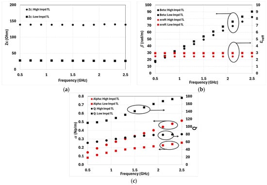
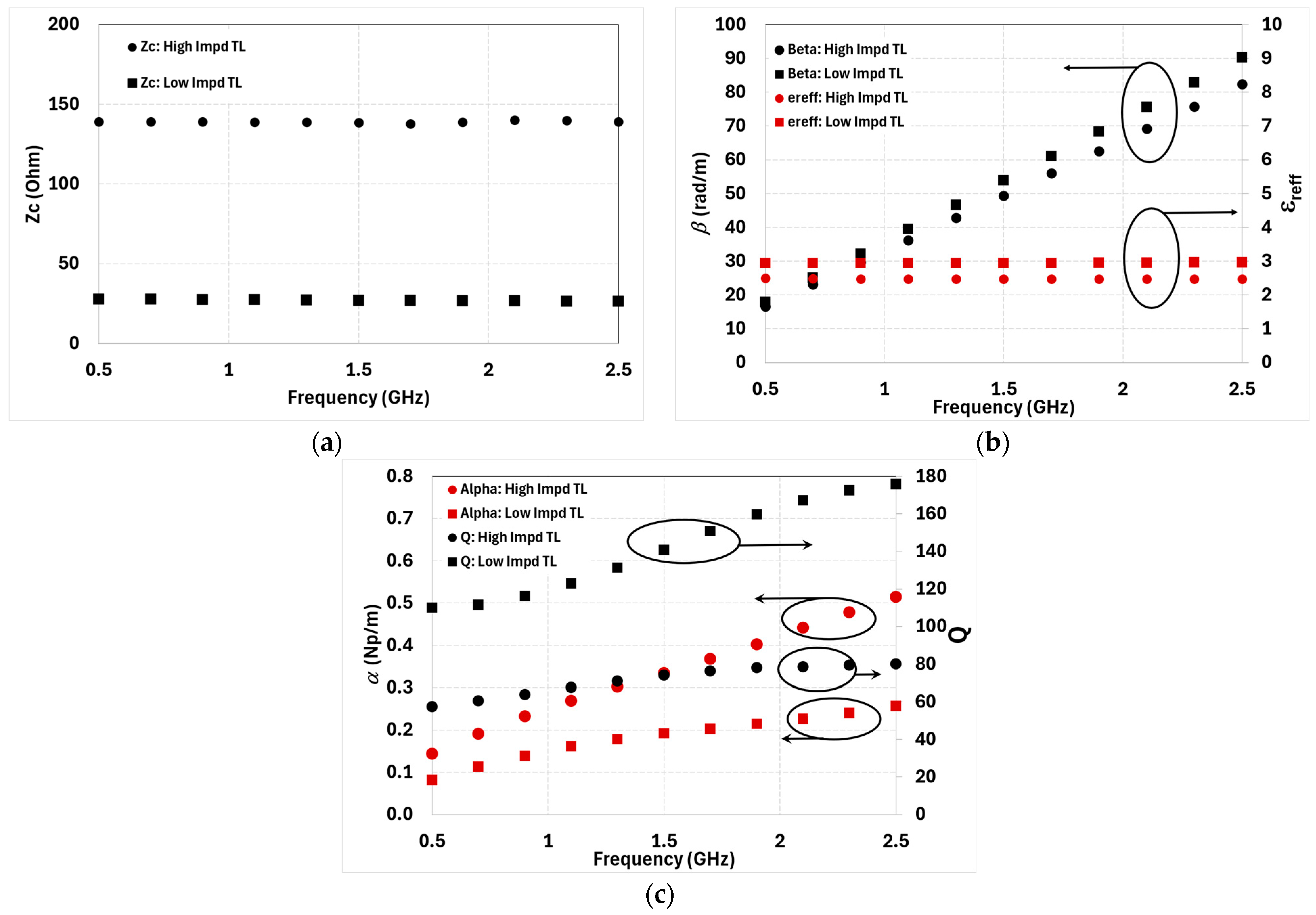
Figure 4a shows the extracted characteristic impedance. The narrow 0.25 mm strip yields a stable high-impedance baseline of approximately 140 Ω, while the wide 8 mm strip leads to a low-impedance baseline of approximately 27 Ω. Analyzing the phase propagation, shown in Figure 4b, reveals a distinct divergence in the effective relative permittivity based on the strip width. The high-impedance line (140 Ω) exhibits a reduced εreff of approximately 2.45. Because the trace is narrow, the parallel-plate capacitance formed with the lower ground plane is minimized, and the fringing fields are less tightly confined by the outer shielding vias. Conversely, the low-impedance line (27 Ω) exhibits a higher εreff of approximately 3. The 8 mm width spans a significant portion of the internal air cavity, forcing an intense, concentrated electric field interaction directly across the air gap and intensifying the capacitive coupling to the vertical shielding walls.
Figure 4.
EM simulations. (a) Characteristic impedance (Zc), (b) β and εreff, (c) α and Q, for high- and low-impedance TLs.
This geometric divergence manifests most critically in the energy dissipation profiles. The high-impedance line (140 Ω) exhibits an increased attenuation constant (α) (Figure 4c), which affects its unloaded quality factor (Q) to a range scaling from roughly 57 at 0.5 GHz to 80 at 2.5 GHz. This penalty is strictly metallic in origin; the constricted 0.25 mm conduction path triggers severe skin depth current crowding, generating higher ohmic resistance [9]. In sharp contrast, the low-impedance line (27 Ω) demonstrates high propagation efficiency. By expanding the strip width to 8 mm, the localized metallic drag is effectively eliminated and the unloaded quality factor scales, climbing from 110 at 0.5 GHz to nearly 175 near the 2.5 GHz boundary.
By defining these rigorous boundary limits, the numerical investigation confirms that the AVIS architecture can reliably sustain a characteristic impedance step-ratio (140 Ω to 27 Ω) while effectively managing dielectric containment. Having mapped these capabilities, these specific extreme strip impedance states provide the exact structural contrast required to synthesize the core resonant elements of the Stepped-Impedance Resonator (SIR) filter.
3. SIR Filter Based on AVIS TLs
To experimentally validate the low-loss propagation characteristics and the extreme characteristic impedance capabilities mapped in Section 2, the AVIS transmission line topology was utilized to synthesize a practical distributed circuit. This section presents the development of a Stepped-Impedance Resonator (SIR) lowpass filter. By cascading alternating high- and low-impedance AVIS segments, this implementation demonstrates the technology’s capacity to maintain strong in-band signal integrity.
3.1. Design Specifications
The proposed AVIS lowpass filter was engineered to support mid-band 5G (Sub-6 GHz) infrastructure, specifically targeting the 3.55 GHz n78 spectrum and cutting off the upper-range C-band (4–8 GHz) signals while prioritizing low in-band insertion loss. The key specifications are:
- Filter Topology and Cutoff Frequency (fc): A Chebyshev lowpass response was considered, featuring a 3-dB cutoff frequency at 3.55 GHz.
- Filter Order and Selectivity: A 7th-order topology was utilized to achieve acceptable frequency selectivity. This ensures effective roll-off performance, providing suppression of out-of-band signals in the 4+ GHz range.
- Passband Performance: The primary operational objective was to minimize in-band insertion loss (S21) (less than 0.5 dB) while maintaining good return loss (better than 15 dB).
- Design Minimalism: The design maintains a pure, classical cascaded SIR topology. The inclusion of layout-intensive complexity enhancers—such as open or shorted stubs, meandered lines, or defected ground structures (DGS)—was explicitly avoided to ensure the filter remains free from the parasitic coupling and electromagnetic leakage often associated with non-standard layout designs. By doing so, the AVIS performance enhancements are isolated and validated as a direct consequence of the inverted shielded configuration rather than additional structural modifications.
3.2. Design
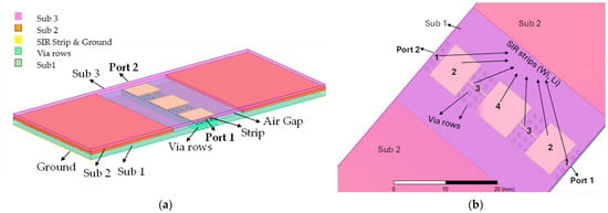
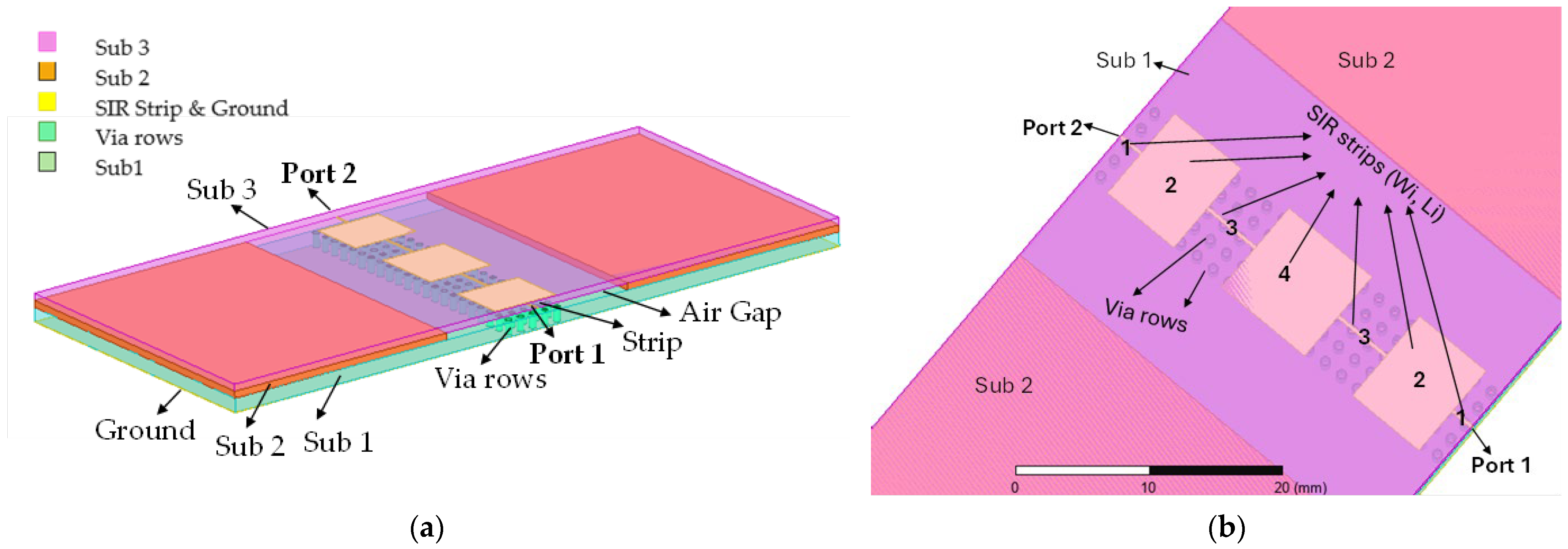
The physical realization of the SIR lowpass filter is illustrated in the 3D isometric and top-down views in Figure 5a,b. The filter was constructed by cascading alternating wide (27 Ω) and narrow (140 Ω) inverted strips, which remain entirely suspended over the routed longitudinal air cavity of the AVIS topology. The filter was directly optimized within Ansys HFSS. The optimized geometric parameters for the 7th-order SIR lowpass filter are summarized in Table 2.
Figure 5.
(a) 3D isometric, (b) and cross-sectional schematic views of the AVIS SIR Filter.
Table 2.
Optimized physical dimensions of the AVIS SIR lowpass filter.
To accommodate the extreme structural geometry of the SIR filter—specifically the wide low-impedance strips (Ws = 8 mm)—the shielding topology is systematically scaled from three to five rows. This expansion is methodologically required to comprehensively span and contain the broader lateral electric fields generated beneath the wide conductive elements.
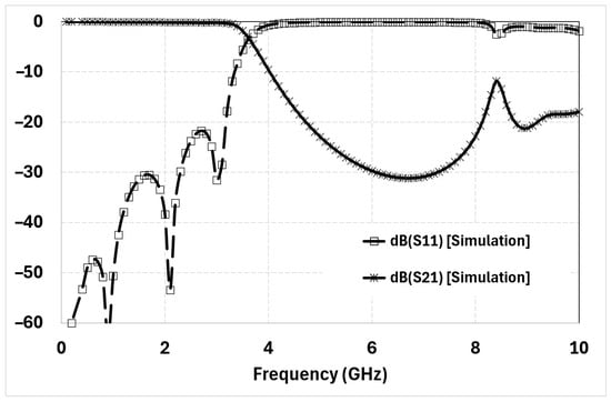
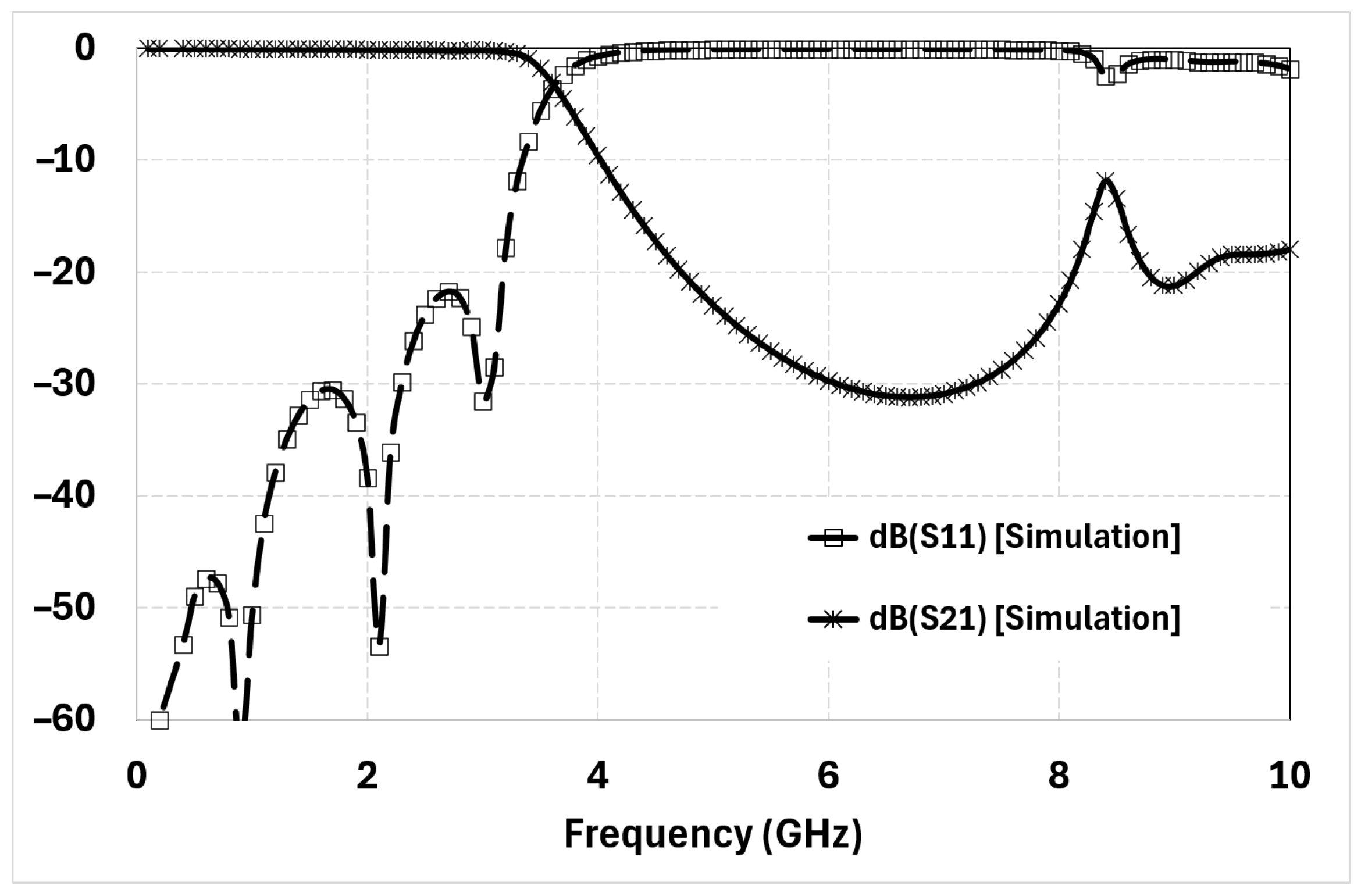
The 7th-order SIR lowpass filter was simulated across the 0 to 10 GHz frequency spectrum. The response is presented in Figure 6. Within the primary operational passband, the insertion loss (S21) remains below 0.18 dB. Concurrently, the return loss (S11) demonstrates good and stable impedance matching, remaining better than 20 dB across the entire defined passband. The 3-dB cutoff frequency occurs precisely at 3.6 GHz. Deep into the stopband, the filter maintains a broad rejection profile, keeping the transmission coefficient (S21) below −20 dB from 4.3 GHz up to approximately 8 GHz.
Figure 6.
Simulation results for the SIR filter.
3.3. Experimental Verification
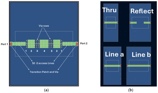
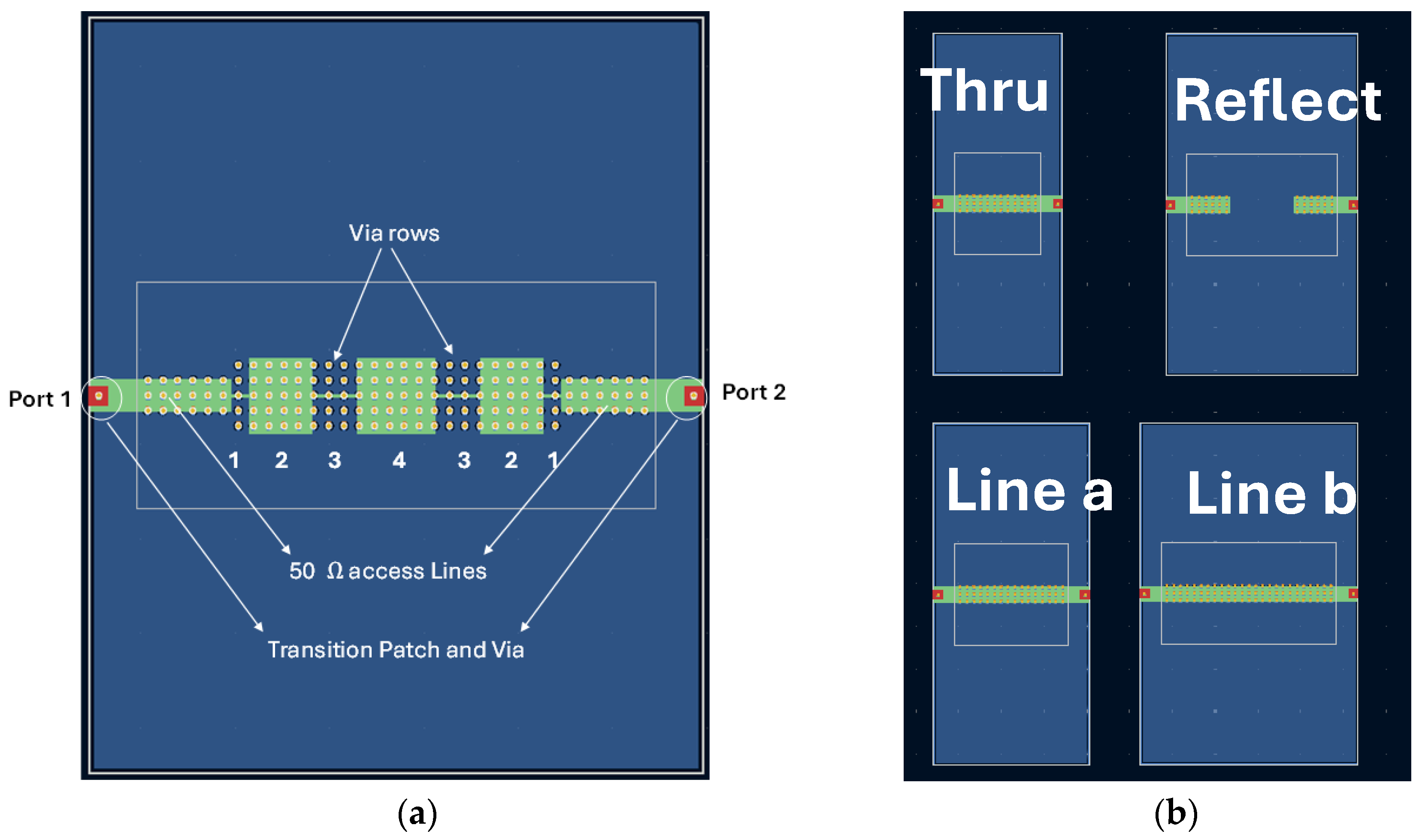
To experimentally validate the simulated performance, the 7th-order AVIS SIR lowpass filter was fabricated. The physical layouts generated for board fabrication are presented in Figure 7a. To physically interface the embedded AVIS structure with standard laboratory equipment, localized copper transition patches and plated vertical transition vias were integrated at both the input and output access lines to accommodate end-launch SMA connectors. A custom TRL calibration kit (Figure 7b) was designed and fabricated simultaneously on the exact same FR4 panel as the filter prototypes. The dimensions of the different components of the calibration kit correspond to those of the filter access lines.
Figure 7.
Physical layout of: (a) the proposed SIR AVIS filter, (b) the TRL kit.
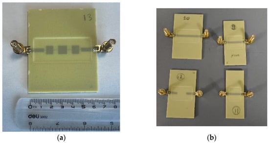
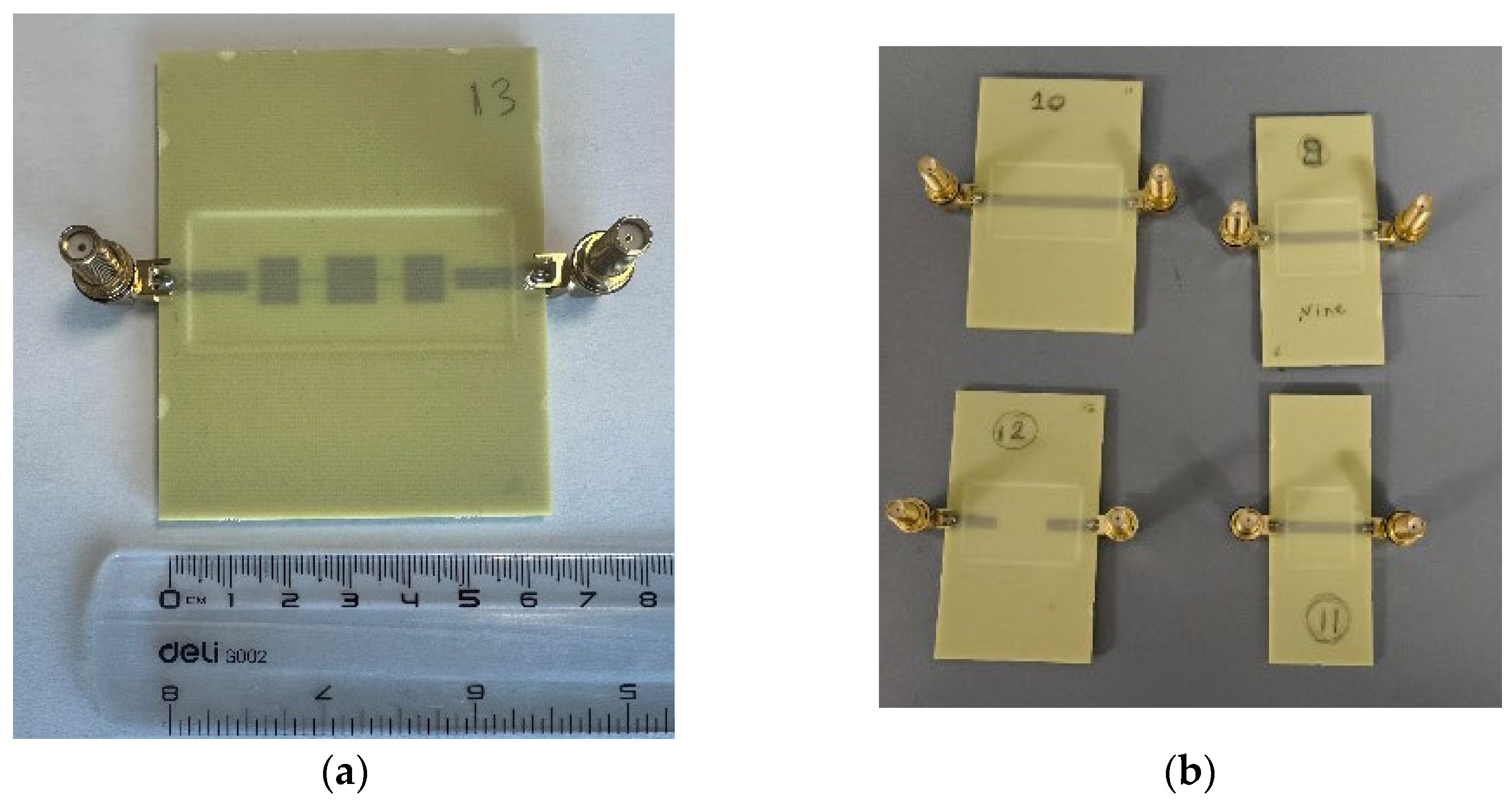
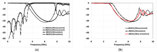
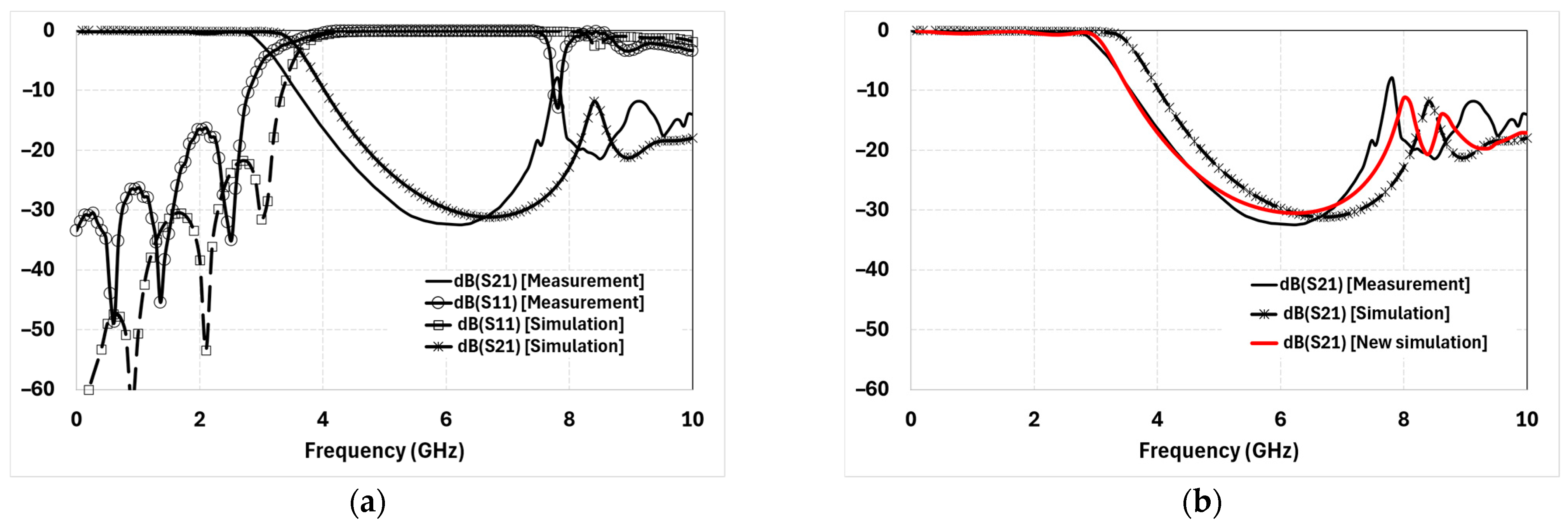
Figure 8a displays the fabricated AVIS SIR filter, and Figure 8b presents the TRL calibration set. S-parameter characterization was carried out utilizing a Rohde & Schwarz ZNB20 VNA. Figure 9a shows the measured versus simulation results for the filter. The measured insertion loss (S21) remains lower than 0.31 dB, and the measured return loss (S11) remains better than 16.2 dB throughout the passband. As the network transitions into the stopband, the measured frequency response exhibits a slight downward frequency shift compared to the simulation. Specifically, the measured 3-dB cutoff frequency occurs at approximately 3.23 GHz (compared to the simulated 3.6 GHz). Because the design utilizes non-critical dimensions, standard PCB etching tolerances are excluded as a contributing factor. Instead, this frequency deviation is attributed to the high-temperature multi-layer FR4 lamination process, where localized thermal subsidence induces a micro-contraction of the air gap layer. This physical compression slightly elevates the effective relative permittivity of the substrate, mathematically scaling the guided wavelength and resulting in the observed downward frequency shift.
Figure 8.
Photograph of the physically fabricated (a) SIR AVIS filter and (b) TRL kit.
Figure 9.
(a) Simulation versus measurement of the AVIS SIR filter, and (b) re-optimization.
To verify the physical origin of the discrepancy between the simulated (3.6 GHz) and measured (3.23 GHz) cutoff frequencies, high-precision mechanical metrology was conducted directly on the fabricated SIR filter prototypes using an LPKF ProtoMat CNC milling platform. The machine’s Z-axis drive features a sub-micron mechanical step resolution (≤0.8 µm) and a stringent repeatability margin (±5 µm), ensuring high-fidelity topological extraction. The rigid, supported perimeter of the PCB was first probed to establish a reference baseline height. The CNC probe was then translated across the mid-span of the suspended substrate directly above the routed air cavity. These physical measurements revealed an intrinsic structural subsidence of 0.11 mm at the center of the span. Consequently, the internal air cavity was physically contracted from its nominal 0.4 mm design height down to an experimentally verified 0.29 mm. By optimizing the air gap height from its nominal 0.4 mm down to 0.29 mm, the simulated response is brought into close agreement with the physical measurements. As illustrated in Figure 9b, this adjusted height effectively accounts for the lamination-induced micro-contraction and better aligns the simulation with the measurement.
3.4. Comparison with the State-of-the-Art
Table 3 presents a comprehensive comparative analysis of the proposed AVIS filter against several similar state-of-the-art implementations of SIR filters [19,20,21,22,23,24,25,26,27,28,29]. In the comparison, ‘Cost’ is classified strictly by the host material: ‘Low Cost’ designates the use of commoditized, standard FR4 substrates, whereas ‘High Cost’ indicates the reliance on premium microwave laminates (e.g., Rogers, RT/duroid, PTFE). ‘Complexity’, on the other hand, is classified by fabrication demands: ‘Low Complexity’ refers to standard planar etching and lamination without structural anomalies; ‘Moderate Complexity’ involves geometric perturbations, such as non-uniform etched ground slots, wiggly-lines, or capacitive surface loading; and ‘High Complexity’ requires advanced manufacturing, such as multi-layer precision milling, 3D mechanical machining, or complex EBG via-fencing. It is important to note that the referenced filters in Table 3 vary in terms of filter order, center frequency, bandwidth, and specific out-of-band rejection levels. While these differing system requirements limit the ability to make direct one-to-one comparisons, the primary comparative metric evaluated here is the relative mitigation of passband insertion loss within the physical constraints of the chosen fabrication materials.
Table 3.
State-of-the-art comparison of similar SIR filters.
As demonstrated in Table 3, the proposed AVIS design achieves a competitive IL of 0.31 dB. When comparing this to the literature, many existing designs utilizing complex, multi-layer stacks or specialized substrates [25,26,27,28,29] report IL values ranging from 0.3 dB up to 4 dB. Furthermore, classical SIR filter approaches [21,22,23,24] demonstrate significantly higher insertion loss, ranging from 1 dB to 4 dB. In contrast, the proposed AVIS filter achieves an IL of 0.31 dB—effectively matching or outperforming these filters—while adhering to the low-cost and low-complexity fabrication standards typical of classical SIR approaches.
4. PCL Filter Based on AVIS TLs
To evaluate the scalability of the AVIS technique across different planar resonant topologies, this section provides the design of a bandpass Parallel-Coupled Line Filter (PCLF).
4.1. Specifications
The proposed PCL filter was designed for a center frequency (f0) of 2.4 GHz, targeting standard wireless communication bands. The design adopts the same shielding via configuration and air cavity integration utilized in the preceding lowpass SIR filter. Table 4 summarizes the performance specifications for the PCL filter. To ensure high predictability and measurement repeatability, the PCL filter design strictly adheres to classical coupled-line synthesis methodologies. This minimalist approach was intentionally selected to ensure a clear performance profile. As with the lowpass filter, this guarantees that the observed characteristics derive directly from the AVIS architecture rather than structural layout enhancements.
Table 4.
Targeted PCLF specifications.
4.2. Filter Design
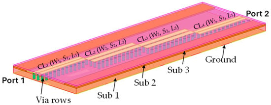
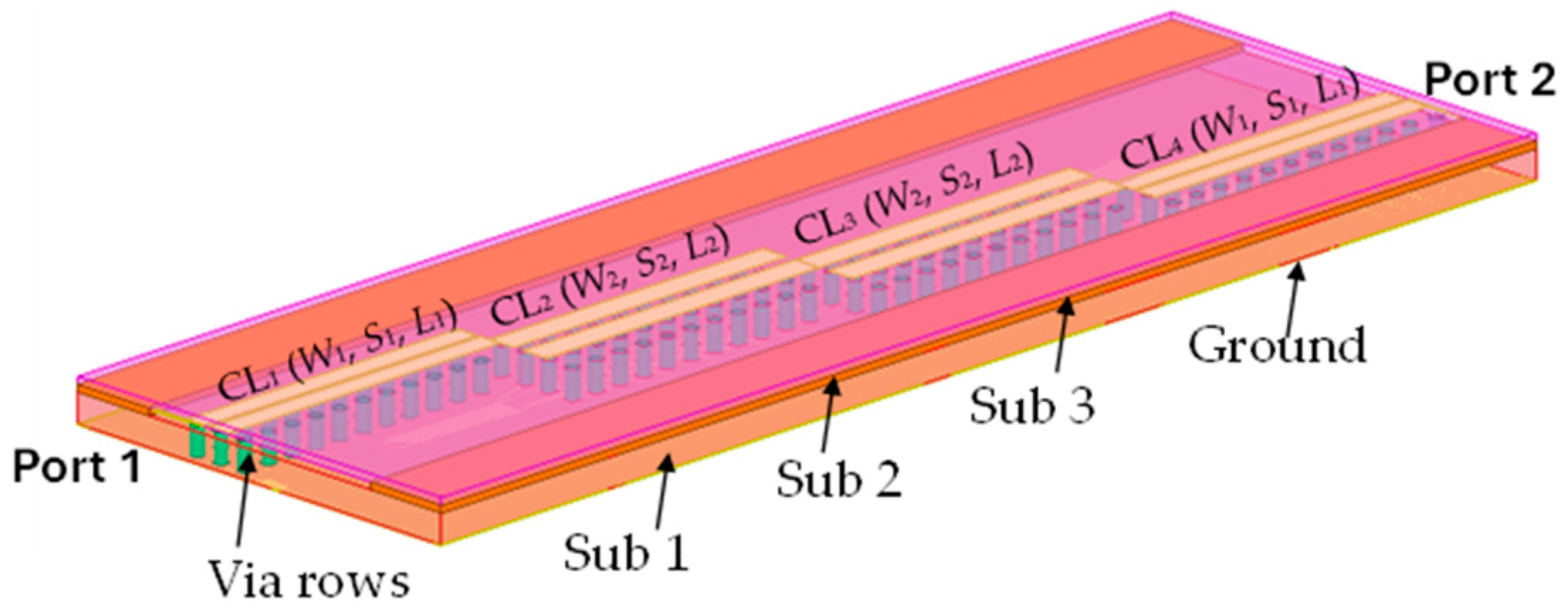
The physical topology of the proposed AVIS-based Parallel-Coupled Line bandpass filter is illustrated in Figure 10. The design consists of four cascaded coupled-line sections, denoted as CL1 through CL4. The geometric parameters for these sections—width (W), spacing (S), and length (L)—were iteratively optimized using Ansys HFSS to achieve the target passband response with a center frequency of 2.4 GHz. The via-shielding parameters, defined by the via diameter and pitch (dv,Xv), were maintained as constant values of 0.8 mm and 1.6 mm, respectively, to ensure fabrication consistency across the entire filter footprint. A distinct feature of this design is the configuration of the shielding via rows. The outer sections, CL1 and CL4, are enclosed by three rows of shielding vias, whereas the central sections, CL2 and CL3, are enclosed by four rows. This hybrid via allocation—utilizing three rows for the outer sections (CL1,CL4) and scaling to four rows for the central sections (CL2,CL3)—was implemented as part of a systematic design workflow to dynamically match electromagnetic containment with the varying strip widths and local field intensities across the coupled-line stages. All the physical parameters of the filter are given in Table 5.
Figure 10.
3D isometric view of the AVIS PCL bandpass filter.
Table 5.
Optimized physical dimensions of the AVIS PCL bandpass filter.
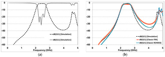
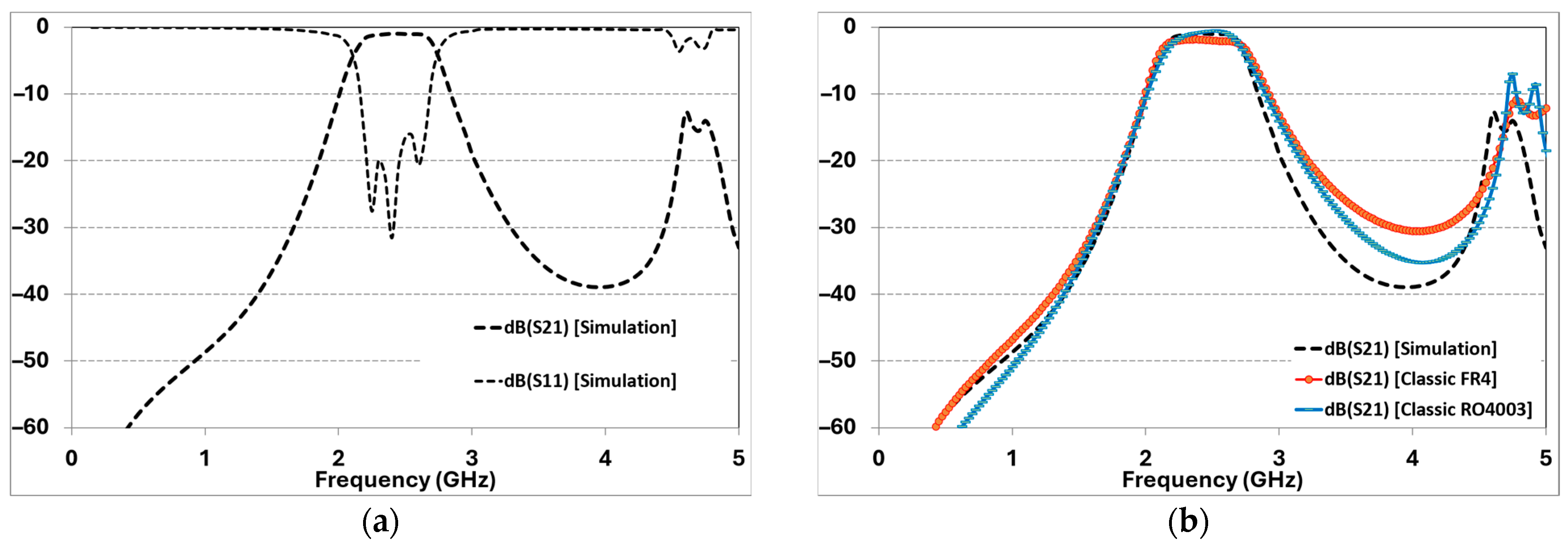
Figure 11a presents the simulated S-parameter response of the optimized AVIS-based PCL bandpass filter. The design demonstrates a center frequency of 2.4 GHz, achieving a passband insertion loss of 0.9 dB. The return loss is better than 16.5 dB within the passband. The FBW is about 27%. The filter exhibits good roll-off characteristics; upper selectivity of 49 dB/GHz and a lower selectivity of 77 dB/GHz. Furthermore, the stopband performance has a 20-dB rejection level achieved up to 4.55 GHz. To further evaluate the mitigation of dielectric losses, Figure 11b compares the simulated insertion loss (S21) of the proposed AVIS PCL filter on standard FR4 against a conventional microstrip PCL filter on standard FR4 and a high-cost Rogers RO4003 laminate. At nearly identical FBWs, the AVIS PCLF achieves a minimum passband insertion loss of 0.9 dB, outperforming the conventional FR4 design (1.9 dB) and approaching the performance of the premium RO4003 substrate (0.6 dB). Consequently, the AVIS topology achieves an in-band insertion loss profile that closely tracks that of the high-performance Rogers RO4003 benchmark, demonstrating that low-cost FR4 can be utilized to achieve high-efficiency microwave filtering without incurring prohibitive material costs.
Figure 11.
(a) Simulation results of the AVIS PCL bandpass filter, and (b) PCL bandpass filter constructed with AVIS and FR4, and Rogers RO4003.
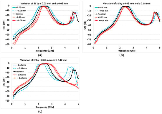
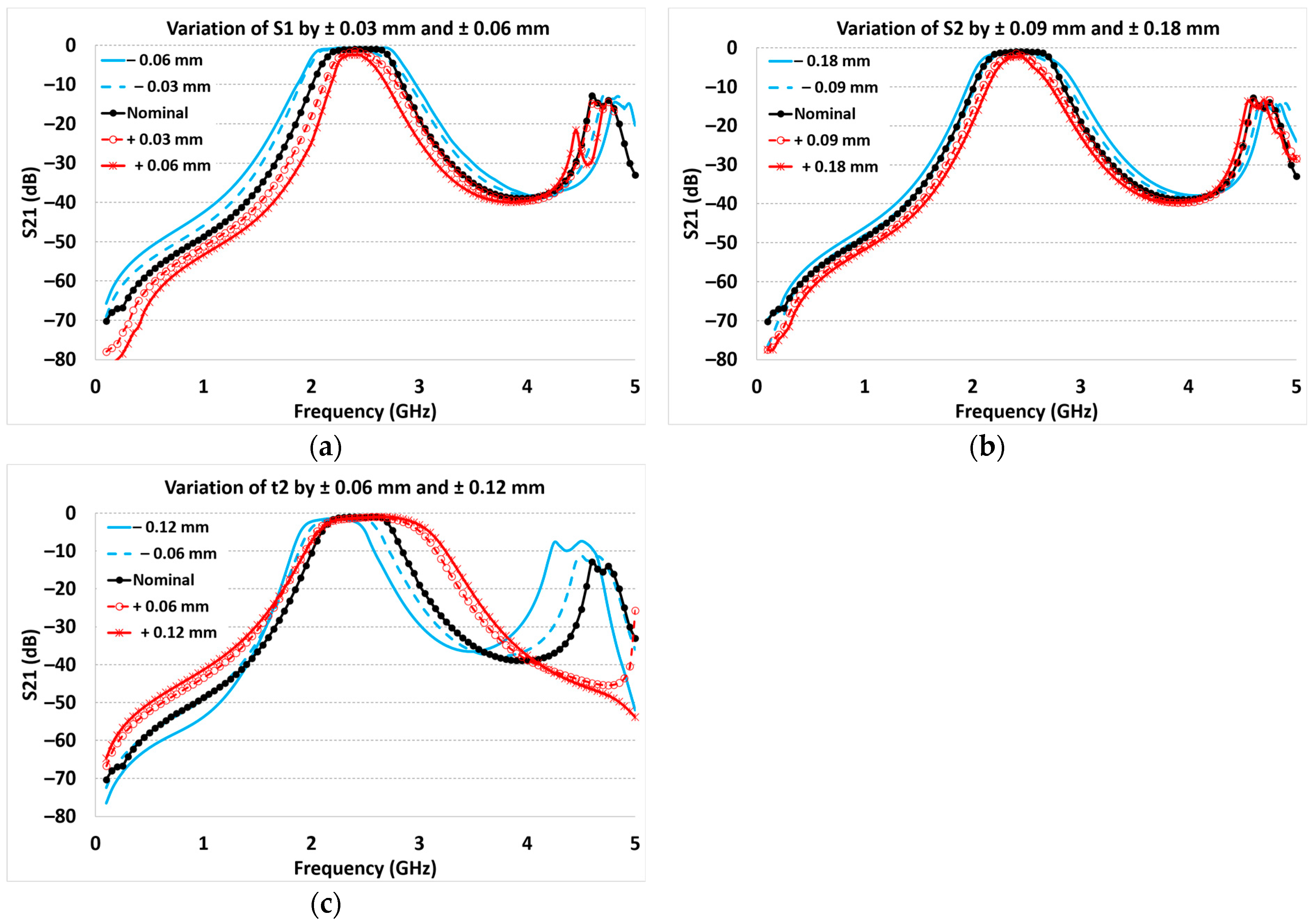
To evaluate the stability of the proposed AVIS structure against realistic manufacturing deviations, a parametric tolerance analysis was conducted using absolute physical bounds centered on the nominal dimensions. Three specific parameters were chosen because they isolate the two orthogonal physical fault lines governing the AVIS fabrication process: lateral lithographic etching variations affecting the coupling structures (S1 and S2), and vertical thermal compression altering the air gap cavity height (t2). Together, they represent the complete operational envelope of the design’s physical vulnerabilities. Figure 12 illustrates the simulated S-parameter response under systematic absolute variations.
Figure 12.
Simulated S-parameter response of the AVIS PCL filter under tolerance variations: (a) S1, (b) S2, and (c) t2.
As shown in Figure 12a, varying S1 around its nominal value by ±0.03 mm and ±0.06 mm affects both the passband insertion loss (−0.63 dB to −2.5 dB) and the fractional bandwidth (33% to 16%). This happens with a marginal frequency shift of less than 50 MHz. Similarly, modifying the inter-resonator coupling gap S2 around its nominal value by ±0.09 mm and ±0.18 mm (Figure 12b) scales both the passband insertion loss (−0.88 dB to −2.4 dB) and the fractional bandwidth (29% to 19%).
In contrast, Figure 12c demonstrates the system’s sensitivity to vertical variations in the air gap spacer height (t2). Compressing or expanding t2 by ±0.06 mm and ±0.12 mm shifts the center frequency up to 200 MHz and results in a fractional bandwidth variation between 27% and 43%.
4.3. Experimental Verification
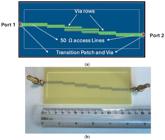
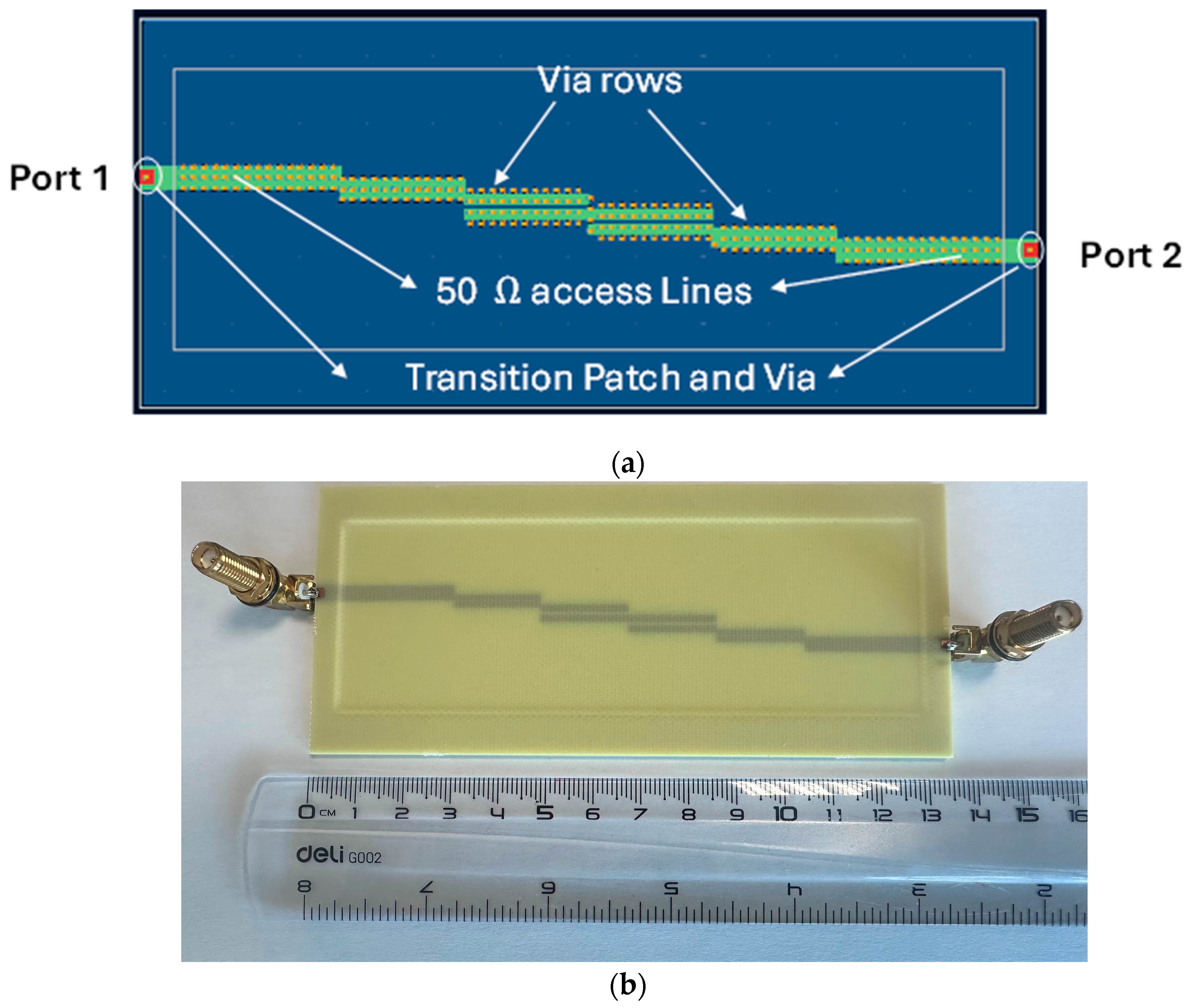
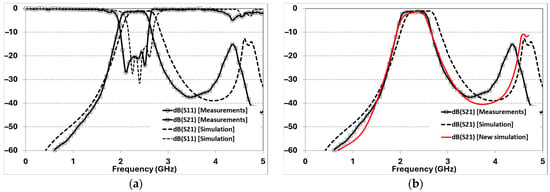
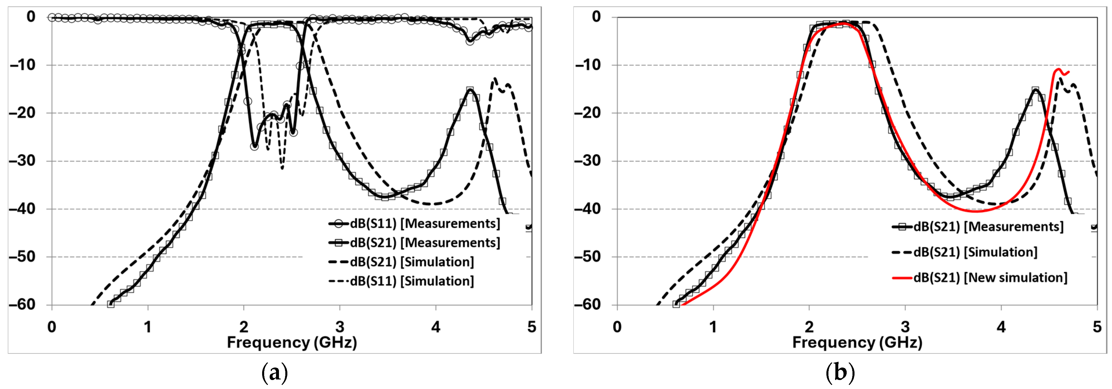
The designed PCL filter was fabricated using standard FR4 processing, with the layout—including the transition patches and 50 Ω access lines—shown in Figure 13. The measured S-parameter performance, plotted alongside the simulated results in Figure 14a, demonstrates a center frequency of 2.3 GHz.
Figure 13.
(a) Physical layout, and (b) fabrication of the AVIS PCL bandpass filter.
Figure 14.
(a) Measurement versus simulation of the PCL filter, and (b) re-optimization of the response.
The measured insertion loss (IL) is 1.1 dB at the center frequency, and the return loss (RL) is better than 18 dB within the passband. The filter achieves a fractional bandwidth (FBW) of 26%. Furthermore, the upper 20 dB rejection level is reached at 4.3 GHz.
To evaluate the practical implications of the observed 100 MHz frequency offset (4% shift), the system architecture must be considered. For tightly regulated, narrow-channel deployments, this structural offset would necessitate proactive pre-fabrication compensation. However, for wideband RF front-ends—such as Cognitive Radio (CR) spectrum sensing nodes, Software-Defined Radio (SDR) receivers, or multi-band RF energy harvesting systems [30]—this shift is tolerable. As established in adaptable RF hardware paradigms [30], strictly adhering to static spectral bounds (fear-based RF design) is less critical than ensuring the desired signal spectrum falls safely within a high-performance filtering plateau. Because the filter features a wide fractional bandwidth (FBW ≈ 26%), its passband spans approximately 600 MHz. Consequently, the shifted passband still completely engulfs primary target spectra, such as the 2.4 GHz ISM band. Within this shifted window, the insertion loss remains stable at 1.1 dB, and the return loss stays better than 18 dB, indicating that wideband signal integrity is not compromised.
A comparison between the simulated and measured results indicates a slight frequency shift and a marginal increase in IL (−0.2 dB), consistent with observations made during the characterization of the SIR filter prototype. This discrepancy can be attributed to two primary factors. First, fabrication tolerances in the PCB etching process—specifically regarding the coupling gap (S) of the PCL sections—directly impact the coupling coefficient and the resonant frequency. Second, during the high-temperature lamination of the multi-layer FR4 board, localized thermal subsidence causes a micro-contraction of the air gap, which slightly elevates the effective relative permittivity of the physical substrate. This increased capacitive coupling mathematically scales the guided wavelength, resulting in the observed downward shift of the passband and stopband resonances.
To investigate the origin of the observed frequency shift, post-fabrication metrology was conducted on the physical PCL filter to extract its true manufactured dimensions. First, mechanical metrology confirmed a lamination-induced cavity contraction, mirroring the SIR filter prototypes, which reduced the internal air gap height to 0.295 mm. Second, a high-contrast transmissive imaging system (Invitrogen iBright 1500) was utilized to optically penetrate the upper FR4 substrate. The system is equipped with a 9.1-megapixel cooled CCD camera featuring a mechanical zoom capability, providing an effective spatial resolution of approximately 32 µm per pixel. These high-resolution optical measurements revealed clear over-etching of the internal coupling gaps. Specifically, the 0.2 mm (S1) physically expanded to approximately 0.25 mm, and the nominal 0.625 mm (S2) expanded to approximately 0.75 mm. Guided by these verified physical metrology results and the structural sensitivity bounds mapped in Figure 12, a refined simulation analysis was conducted. The simulated response is brought into close agreement with the measurement, as shown in Figure 14b.
Despite the observed discrepancy between simulation and measurement, the experimental results demonstrate the potential of the proposed multi-layer structure, which exhibits relatively low insertion loss. Improved control of fabrication technology is required to achieve better performance consistency. However, this is primarily a process characterization issue and therefore lies beyond the scope of this paper.
4.4. Comparison with Literature
Table 6 provides a comparison against some PCL designs reported in the literature [31,32,33,34,35,36,37,38,39,40,41,42,43,44]. These works share key characteristics with the work proposed in this paper: specifically, they utilize Parallel-Coupled Line (PCL) topologies and operate at comparable center frequencies and fractional bandwidths (FBW). As with the prior comparison, the referenced PCL designs exhibit natural variations in filter order, exact fractional bandwidth, and spurious rejection levels. Acknowledging these differing design constraints, the primary focus of this comparison remains the localized trade-off between passband electrical efficiency and bulk substrate cost. As the data demonstrate, conventional PCL designs on standard FR4 substrates exhibit much higher insertion loss, typically exceeding 2.7 dB [31,32,33,34,42,43,44], while achieving competitive performance metrics—such as deep spurious rejection. On the other hand, PCLF on high-cost substrates [35,37,38,39,40,41] or complex 3D fabrication methods [40,44] achieve higher IL than the presented work. The proposed AVIS PCL filter distinguishes itself by achieving a competitive insertion loss of 1.1 dB and moderate selectivity without sacrificing fabrication simplicity or material cost. This comparison emphasizes the efficacy of the AVIS approach in overcoming the performance-to-cost trade-off inherent in conventional microstrip filter design, positioning it as an effective and suitable solution for high-performance microwave applications.
Table 6.
State-of-the-art comparison of similar PCL filters.
Beyond the improvements in insertion loss, the AVIS PCL filter demonstrates a notable reduction in physical footprint compared to conventional designs. With a compact surface area of 1490 mm2, the proposed structure occupies significantly less real estate than standard planar PCL filters [31,32,34,36], which typically range from 1800 mm2 to 2800 mm2 for similar center frequencies. This compactness is achieved without the need for complex, high-resolution geometric perturbations—such as corrugated or wiggly-line patterns [37,38]—or high-dielectric materials that would otherwise increase fabrication cost. Consequently, the AVIS architecture provides a competitive balance of performance-to-size-to-cost ratio.
While this work employs a classic Parallel-Coupled Line topology to ensure design robustness and fabrication reliability, the AVIS framework is inherently flexible and compatible with advanced coupling mechanisms. Techniques reported in the literature—such as the over-coupled stages [41] or the geometric perturbations (e.g., wiggly-lines or corrugated edges) [38]—are adaptable to the proposed structure. Integrating these coupling strategies into the AVIS topology would be a straightforward extension, potentially yielding even sharper roll-off characteristics and enhanced stopband rejection. Consequently, the proposed AVIS approach serves not only as a high-performance solution in its current form but also as a versatile platform that can be further optimized for specific, high-selectivity microwave applications.
5. Conclusions
This paper presented the Air-Void Inverted Shielded (AVIS) transmission line topology, designed to decouple electromagnetic wave propagation from the dissipative nature of low-cost FR4 substrates. The proposed framework was validated through the design and fabrication of a 7th-order SIR lowpass filter and a 3rd-order PCL bandpass filter. Both components demonstrated high in-band signal integrity, achieving insertion loss of 0.31 dB and 1.1 dB, respectively. While achieving strict performance consistency requires further refinement of the manufacturing tolerances, this process characterization falls outside the current scope. These results confirm that the AVIS topology offers a robust platform that enables high-performance microwave filtering on standard, mass-market PCB materials, effectively overcoming the traditional trade-off between electrical efficiency and manufacturing cost. While this study employed foundational Stepped-Impedance Resonator (SIR) and Parallel-Coupled Line (PCL) topologies as controlled benchmarks to strictly isolate and validate the performance enhancements of the AVIS architecture, the proposed technique serves as an adaptable design platform. Future work is currently extending this framework to more advanced, modern structures—such as dual-mode resonant configurations, compact multi-band filtering networks, and substrate-integrated components—to further optimize performance for emerging high-frequency wireless applications.
Author Contributions
Conceptualization, P.F. and H.I.; methodology, D.K., P.F. and H.I.; software, H.I.; validation, D.K., P.F. and H.I.; formal analysis, D.K., P.F. and H.I.; investigation, H.I.; resources, P.F.; data curation, D.K. and H.I.; writing—original draft preparation, H.I.; writing—review and editing, D.K., P.F. and H.I.; visualization, D.K., P.F. and H.I.; supervision, P.F. and H.I.; project administration, H.I. All authors have read and agreed to the published version of the manuscript.
Funding
This research received no external funding.
Data Availability Statement
All data are contained within the article. Further inquiries can be directed to the corresponding authors.
Conflicts of Interest
The authors declare no conflicts of interest.
References
- Sepaintner, F.; Scharl, A.; Röhrl, F.X.; Bogner, W.; Zorn, S.Z. Simulation and Manufacturing of Low Loss PCB Structures with Additional Electromagnetic Field in Air. In Proceedings of the 2019 IEEE MTT-S International Microwave Workshop Series on Advanced Materials and Processes for RF and THz Applications (IMWS-AMP), Bochum, Germany, 16–18 July 2019; pp. 94–96. [Google Scholar] [CrossRef] [Scilit]
- Sepaintner, F.; Scharl, A.; Jakob, J.; Keck, F.; Kunze, K.; Rohrl, F.X.; Bogner, W.; Zorn, S. Cost-Effective Implementation of Air-Filled Waveguides on Printed Circuit Boards. In Proceedings of the 2020 IEEE 29th Conference on Electrical Performance of Electronic Packaging and Systems (EPEPS), San Jose, CA, USA, 5–7 October 2020; pp. 1–3. [Google Scholar] [CrossRef] [Scilit]
- Sun, C.-S.; Li, X.-C.; Zhang, H.-B.; Mao, J.-F. A Low-Cost Hollow Rectangular Dielectric Waveguide. In Proceedings of the 2023 IEEE MTT-S International Wireless Symposium (IWS), Qingdao, China, 14–17 May 2023; pp. 1–3. [Google Scholar] [CrossRef] [Scilit]
- Takamatsu, K.; Tobana, T.; Isota, Y.; Sasamori, T. Analysis of transmission characteristic of a microstrip line placed above a ground slot. In Proceedings of the 2016 International Symposium on Electromagnetic Compatibility-EMC EUROPE, Wroclaw, Poland, 5–9 September 2016; pp. 94–99. [Google Scholar] [CrossRef] [Scilit]
- Akiyama, H.; Tobana, T.; Isota, Y. Study of Propagation Characteristic Analysis of a Microstrip Line Placed on Ground Slot Asymmetrically. In Proceedings of the 2019 Joint International Symposium on Electromagnetic Compatibility, Sapporo and Asia-Pacific International Symposium on Electromagnetic Compatibility (EMC Sapporo/APEMC), Sapporo, Japan, 3–7 June 2019; pp. 309–312. [Google Scholar] [CrossRef] [Scilit]
- Coonrod, J. Microstrip defected ground structures without radiation loss using multilayer PCB technology. Microw. J. 2014, 61, 12–15. [Google Scholar]
- Aziz, M.A.; Issa, H.; Kaddour, D.; Podevin, F.; Safwat, A.M.E.; Pistono, E.; Duchamp, J.; Vilcot, A.; Fournier, J.; Ferrari, P. Shielded coplanar striplines for RF integrated applications. Microw. Opt. Technol. Lett. 2009, 51, 352–358. [Google Scholar] [CrossRef] [Scilit]
- Abdel-Rahman, A.B.; Kheir, M.; Verma, A.K.; Omar, A. Material-Loaded High Q-Factor Slot Resonator and Measurement of Relative Permittivity. Prog. Electromagn. Res. C 2010, 13, 67–76. [Google Scholar] [CrossRef] [Scilit][Green Version]
- Franc, A.-L.; Kaddour, D.; Issa, H.; Pistono, E.; Corrao, N.; Fournier, J.-M.; Ferrari, P. Slow-wave high performance shielded CPW transmission lines: A lossy model. In Proceedings of the 2009 European Microwave Conference (EuMC), Rome, Italy, 29 September–1 October 2009; pp. 185–188. [Google Scholar] [CrossRef] [Scilit]
- Pérez-Fajardo, A.; Cortés-Hernández, D.M.; Torres-Torres, R.; Torres-Jácome, A. Characterization of transmission lines in a novel high-frequency laminate. In Proceedings of the 2016 IEEE 7th Latin American Symposium on Circuits & Systems (LASCAS), Florianopolis, Brazil, 28 February–2 March 2016; pp. 391–394. [Google Scholar] [CrossRef] [Scilit]
- Lee, S.-N.; Lee, J.-I.; Kim, Y.-J.; Yook, J.-G. Low-Loss Thin Film Microstrip Lines and Filters Based on Magnetorheological Finishing. IEEE Trans. Compon. Packag. Technol. 2007, 30, 849–854. [Google Scholar] [CrossRef] [Scilit]
- Narita, K.; Kushta, T. An accurate experimental method for characterizing transmission lines embedded in multilayer printed circuit boards. IEEE Trans. Adv. Packag. 2006, 29, 114–121. [Google Scholar] [CrossRef]
- Han, J.K.; Park, D.C. Crosstalk Analysis Between Non-Parallel Coupled Lines Connected with Vias in a 4-layer PCB. In Proceedings of the 2006 4th Asia-Pacific Conference on Environmental Electromagnetics, Dalian, China, 1–4 August 2006; pp. 728–731. [Google Scholar] [CrossRef] [Scilit]
- Sanchez-Cabello, C.; Herran, L.F.; Rajo-Iglesias, E. Ka-Band Diplexer for 5G mmWave Applications in Inverted Microstrip Gap Waveguide Technology. Electronics 2020, 9, 2094. [Google Scholar] [CrossRef] [Scilit]
- Inclán-Sánchez, L. Inverted Microstrip Gap Waveguide Filtering Antenna Based on Coplanar EBG Resonators. Sensors 2023, 23, 282. [Google Scholar] [CrossRef] [Scilit]
- Issa, H.; Duchamp, J.-M.; Abou-Chahine, S.; Ferrari, P. Loaded miniature transmission lines compatible with low cost substrates: Q-factor improvement. In Proceedings of the 40th European Microwave Conference, Paris, France, 28–30 September 2010; pp. 1218–1221. [Google Scholar] [CrossRef] [Scilit]
- Zhang, H.; Zhang, Q.; Liu, J.; Tang, W.; Fan, Y.; Cui, T. Smaller-loss planar SPP transmission line than conventional microstrip in microwave frequencies. Sci. Rep. 2016, 6, 23396. [Google Scholar] [CrossRef] [Scilit]
- Gu, J.; Wang, C.; Sun, X. A frequency selective microstrip line using compensated spiral compact microstrip resonant cells (C-SCMRC). In Proceedings of the 2005 Asia-Pacific Microwave Conference, Suzhou, China, 4–7 December 2005; pp. 1–4. [Google Scholar] [CrossRef] [Scilit]
- Zhang, J.; Yang, R.; Zhang, C. High-Performance Low-Pass Filter Using Stepped Impedance Resonator and Defected Ground Structure. Electronics 2019, 8, 403. [Google Scholar] [CrossRef] [Scilit]
- Gupta, D.; Upadhyay, A.; Yadav, M.; Singhal, P.K. Design and analysis of low pass planer microwave filter using left handed SRR structures. In Proceedings of the 2014 International Conference on Medical Imaging, M-Health and Emerging Communication Systems (MedCom), Greater Noida, India, 7–8 November 2014; pp. 40–44. [Google Scholar] [CrossRef] [Scilit]
- Das, A.; Roy, A.; Roy, K.; Bhattacharyya, A.; Chowdhury, D.; Paul, S. Design and analysis of microwave stepped impedance low pass filter for Bluetooth application. In Proceedings of the 2015 IEEE International Conference on Electrical, Computer and Communication Technologies (ICECCT), Coimbatore, India, 5–7 March 2015; pp. 1–3. [Google Scholar] [CrossRef] [Scilit]
- Romero, M.C.; Reyes-Ayala, M.; Andrade-Gonzalez, E.A.; Chavez-Sanchez, S.; Terres-Peña, H.; Salgado-Guzman, G.; Rodriguez-Rivera, R. Algorithm to Calculate PCB Stepped-Impedance Low-Pass Filters for Microwave Applications. WSEAS Trans. Commun. 2025, 24, 17–22. [Google Scholar] [CrossRef] [Scilit]
- Mitra, S.; Kumuda, D.K. Stepped impedance microstrip low-pass filter implementation for S-band application. Int. J. Latest Trends Eng. Technol. 2015, 5, 248–255. [Google Scholar]
- Neemuchwala, M.; Gupta, S.; Kadam, A. Design and Implementation of Microstrip Line Based Stepped Impedance Low Pass Filter. Int. J. Eng. Res. Technol. 2021, 9, 217–220. [Google Scholar]
- El-Halabi, H.; Issa, H. A compact stepped impedance 7th order microstrip filter. In Proceedings of the 2018 5th International Conference on Electrical and Electronic Engineering (ICEEE), Istanbul, Turkey, 3–5 May 2018; pp. 52–55. [Google Scholar] [CrossRef] [Scilit]
- Verma, A.K.; Chaudhari, N.P.; Kumar, A. Improved performance step impedance lowpass filter. AEU-Int. J. Electron. Commun. 2013, 67, 761–770. [Google Scholar] [CrossRef] [Scilit]
- Yang, Y.; Zhu, X.; Karmakar, N.C. Design of a novel microstrip lowpass filter for UWB chipless RFID readers. In Proceedings of the 2011 Asia-Pacific Microwave Conference, Melbourne, VIC, Australia, 5–8 December 2011; pp. 98–101. [Google Scholar]
- Ma, K.; Yeo, K.S. Novel low cost compact size planar low pass filters with deep skirt selectivity and wide stopband rejection. In Proceedings of the 2010 IEEE MTT-S International Microwave Symposium, Anaheim, CA, USA, 23–28 May 2010; pp. 233–236. [Google Scholar] [CrossRef] [Scilit]
- Lin, Q.; Wang, X.; Wu, Y.; Wu, H.; Li, S. A High-Impedance Line Self-Packaged Low-Pass Filter Based on SISL Technique. Electronics 2025, 14, 4139. [Google Scholar] [CrossRef] [Scilit]
- Chappell, W.J.; Naglich, E.J.; Maxey, C.; Guyette, A.C. Putting the Radio in “Software-Defined Radio”: Hardware Developments for Adaptable RF Systems. Proc. IEEE 2014, 102, 307–320. [Google Scholar] [CrossRef] [Scilit]
- Othman, A.R.; Wasli, C. 2.4 GHz Microstrip Band Pass Filter. In Proceedings of the First International Conference on Engineering and ICT (ICEI), Melaka, Malaysia, 27–28 November 2007. [Google Scholar]
- Gunjal, S.; Pawase, R.S. Design And Implementation Of Microstrip Bandpass Filter Using Parallel Coupled Line For ISM Band. Int. J. Adv. Res. Innov. Ideas Educ. 2016, 2, 3059–3063. [Google Scholar]
- Fatah, S.Y.A.; Taher, F.; Mohamadien, K.H.; Haweel, M.T.; Sree, M.F.A. Design A Microstrip Bandpass Filter Antenna from 2 GHz to 4.7 GHz for Biomedical Applications. In Proceedings of the 2022 32nd International Conference on Computer Theory and Applications (ICCTA), Alexandria, Egypt, 17–19 December 2022; pp. 183–189. [Google Scholar] [CrossRef] [Scilit]
- Gunjal, A.; Gagare, S.; Labade, R. Microstrip Coupled Band Pass Filter using Parallel Coupled Lines used for EMI Reduction. Int. J. Adv. Eng. Res. Sci. 2016, 3, 21–24. [Google Scholar]
- Worapishet, A.; Srisathit, K.; Surakampontorn, W. Stepped-Impedance Coupled Resonators for Implementation of Parallel Coupled Microstrip Filters With Spurious Band Suppression. IEEE Trans. Microw. Theory Tech. 2012, 60, 1540–1548. [Google Scholar] [CrossRef] [Scilit]
- Fathelbab, W.M.; Steer, M.B. Parallel-coupled line filters with enhanced stopband performances. IEEE Trans. Microw. Theory Tech. 2005, 53, 3774–3781. [Google Scholar] [CrossRef] [Scilit]
- Kuo, J.-T.; Hsu, W.-H.; Huang, W.-T. Parallel coupled microstrip filters with suppression of harmonic response. IEEE Microw. Wirel. Compon. Lett. 2002, 12, 383–385. [Google Scholar] [CrossRef] [Scilit]
- Lopetegi, T.; Laso, M.; Hernandez, J.; Bacaicoa, M.; Benito, D.; Garde, M.; Sorolla, M.; Guglielmi, M. New microstrip “Wiggly-Line” filters with spurious passband suppression. IEEE Trans. Microw. Theory Tech. 2001, 49, 1593–1598. [Google Scholar] [CrossRef] [Scilit]
- Sung, Y.; Ahn, C.S.; Kim, Y.-S. Parallel-coupled microstrip bandpass filters with a wide stopband using spur lines. Microw. Opt. Technol. Lett. 2004, 43, 9–11. [Google Scholar] [CrossRef] [Scilit]
- Kuo, J.-T.; Jiang, M.; Chang, H.-J. Design of parallel-coupled microstrip filters with suppression of spurious resonances using substrate suspension. IEEE Trans. Microw. Theory Tech. 2004, 52, 83–89. [Google Scholar] [CrossRef]
- Jiang, M.; Wu, M.-H.; Kuo, J.-T. Parallel-coupled microstrip filters with over-coupled stages for multispurious suppression. In Proceedings of the 2005 IEEE MTT-S International Microwave Symposium Digest, Long Beach, CA, USA, 12–17 June 2005; pp. 687–690. [Google Scholar] [CrossRef] [Scilit]
- Dabhi, V.; Dwivedi, V.V. Analytical study and realization of microstrip parallel coupled bandpass filter at 2 GHz. In Proceedings of the 2016 International Conference on Communication and Electronics Systems (ICCES), Coimbatore, India, 21–22 October 2016; pp. 1–4. [Google Scholar] [CrossRef] [Scilit]
- Dabhi, M.; Dwivedi, V.V. Parallel coupled microstrip bandpass filter designed and modeled at 2 GHz. In Proceedings of the 2016 International Conference on Signal Processing, Communication, Power and Embedded System (SCOPES), Paralakhemundi, India, 3–5 October 2016; pp. 461–466. [Google Scholar] [CrossRef] [Scilit]
- Srivastava, S.; Manjunath, R.K.; Shanthi, P. Design, Simulation and Fabrication of a Microstrip Bandpass Filter. Int. J. Sci. Eng. Appl. 2014, 3, 154–158. [Google Scholar]

Disclaimer/Publisher’s Note: The statements, opinions and data contained in all publications are solely those of the individual author(s) and contributor(s) and not of MDPI and/or the editor(s). MDPI and/or the editor(s) disclaim responsibility for any injury to people or property resulting from any ideas, methods, instructions or products referred to in the content. |
© 2026 by the authors. Licensee MDPI, Basel, Switzerland. This article is an open access article distributed under the terms and conditions of the Creative Commons Attribution (CC BY) license.