


Abstract
The phase-shifted full-bridge high-frequency-link (PSFB-HFL) inverter adopts a DC to sinusoidal-half-wave to sinusoidal-wave conversion structure, which uses few passive components with small parameter values, and the switching frequency of the subsequent stage is low, resulting in low losses. This makes it well suited for airborne applications requiring large currents on the low-voltage side and a high step-up ratio, and it has the potential to realize combined three-phase output. To meet the dynamic-performance requirements of this structure, this paper adopts a peak current control strategy. However, this control method suffers from a sub-harmonic oscillation problem, for which a corresponding slope compensation scheme is designed. Furthermore, based on the small-signal model of the Buck converter, an accurate small-signal model of the PSFB peak current inner loop, based on the average value of the filter inductor current, is derived. Accordingly, a voltage-outer-loop PI controller is designed to implement closed-loop control and improve the dynamic performance of the system. An experimental prototype of a PSFB-HFL inverter with a 28 V DC input and a rated power of 4 kW was built. Experimental results show that the proposed control strategy ensures robust large-signal stability, maintaining high-quality sinusoidal waveforms under varying load conditions, thus verifying the effectiveness and engineering feasibility of the PSFB-HFL inverter.
1. Introduction
With the development of more electric aircraft (MEA) and all-electric aircraft (AEA) technologies, the quantity and capacity of airborne electrical equipment keep increasing [1,2]. Research on power converters with a high power rating, high power density and high electromagnetic compatibility (EMC) has become increasingly significant [3,4]. Meanwhile, to achieve a highly reliable power supply, modern large-size aircraft are equipped with not only a certain number of main generators but also one or multiple auxiliary power units (APUs) serving as emergency and ground-power-supply sources [5]. As critical onboard equipment for normal flight operation and an essential safeguard under emergency conditions, the APU requires a series of electric-energy conversion for startup, whose core component is the start power unit (SPU) [6,7]. Essentially a power converter, the SPU realizes power conversion from 28 V DC input to 115 V/750 Hz three-phase AC output to assist APU startup and features a high power rating, high step-up ratio and short-time-duty operation. In addition, isolated inverters with high power and a high step-up ratio also cover other aerospace secondary-power conversion demands, such as 28 V DC to 220 V/50 Hz AC and 28 V DC to 115 V/400 Hz AC. In recent years, for hybrid power-supply systems of AEA, Reference [8] proposed a novel magnetic-integration high-efficiency converter with low ripple and a favorable dynamic response; Reference [9] reviewed the challenges and opportunities of power electronic design for all and hybrid-electric aircraft and pointed out that high power density and high efficiency constitute the future development trend. Therefore, with the advancement of power electronics technology, research on high power and high step-up ratio isolated inverters for aerospace applications is of great significance.
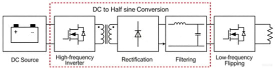
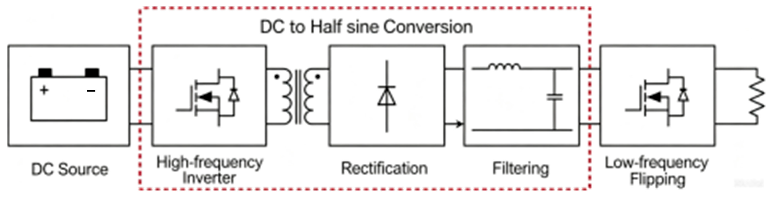
This paper proposes a phase-shifted full-bridge high-frequency-link (PSFB-HFL) inverter with high power and a high step-up ratio for airborne applications, which is shown in Figure 1. Compared with the conventional two-stage DC–DC–AC converter, the proposed topology exhibits the following merits. First, it achieves compact overall volume. The LC filter of the phase-shifted full-bridge (PSFB) DC–DC circuit is required to rapidly respond to the half-sine-wave voltage output, which allows small-value filter parameters and reduced component size. Moreover, no additional LC filter is needed for the final sinusoidal AC output, further shrinking the total system volume. Second, favorable EMC performance is obtained. Soft-switching operation can be realized in the PSFB DC–DC stage, and the level-flipping circuit operates at a much lower frequency than conventional single-phase inverters, which greatly improves the electromagnetic compatibility of the system. Third, full-digital control is adopted. By utilizing the inherent self-suppression capability against transformer winding volt-second unbalance of the primary-side peak current control for the PSFB DC–DC circuit, the conventional DC-blocking capacitor can be eliminated to further reduce volume. Meanwhile, digital control offers advantages such as easy implementation of advanced control algorithms, high flexibility and convenient maintenance. Nevertheless, peak current control suffers from the inherent drawback of sub-harmonic oscillation when the duty cycle exceeds 50%. Without proper suppression, periodic distortion of inductor current or even system instability may occur. This issue becomes especially severe for the low-voltage high-current, high step-up-ratio application investigated in this work.
Figure 1.
Block diagram of PSFB-HFL.
At present, some research foundations have been established regarding the mechanism of sub-harmonic oscillation in peak current mode control and the design of slope compensation. Reference [10] points out that the conventional average state-space modeling method fails to interpret sub-harmonic oscillations occurring above half of the switching frequency and accordingly proposes a discrete small-signal modeling approach in the z-domain, which provides a theoretical basis for the engineering design of slope compensation. Reference [11] develops a slope compensation scheme for DC–DC converters and verifies its suppression performance against sub-harmonic oscillations under various operating conditions. Reference [12] investigates feedforward compensation for the dynamic characteristics of PSFB converters under peak current mode control. Nevertheless, most of the above-mentioned studies target conventional topologies such as Buck and push–pull converters or focus merely on the stability of the converter itself.
In parallel with control-theoretic approaches to power electronic converters, recent years have witnessed significant advances in uncertainty-aware optimization methods for complex energy systems. For instance, Tan et al. [13] proposed a stochastic weight robust optimization (SWRO) framework that partitions the uncertainty set into multiple sub-intervals and incorporates their probabilistic information as weights in the objective function, thereby achieving a principled trade-off between robustness against adverse scenarios and economic efficiency—avoiding the excessive conservatism of traditional worst-case robust optimization. Furthermore, the introduction of an expected robust cost (ERC) methodology enables automatic determination of asymmetric uncertainty bounds, balancing operational costs with potential risks of renewable energy curtailment and load shedding. Although these methods were developed in the context of microgrid-transportation networks, the underlying design idea of uncertainty-aware robustness is directly relevant to our work: the proposed PSFB-HFL inverter control strategy similarly incorporates conservative stability margins to ensure reliable operation under varying load conditions and renewable energy fluctuations, where the small-signal and large-signal stability criteria are explicitly defined to address different classes of uncertainties.
The specific shortcomings of existing methods can be summarized as follows: (1) most small-signal models are established based on the state-space averaging method or harmonic linearization method, which assume that the switching frequency is significantly higher than the fundamental frequency, but in the PSFB-HFL inverter adopting the DC to half-sine-wave to sine-wave conversion architecture, the effective duty cycle loss caused by the resonant inductor and transformer coupling significantly affects the small-signal dynamics, and these conventional methods fail to accurately capture this effect; (2) existing peak current mode control models typically do not consider the influence of the filter inductor current on the secondary side of the PSFB circuit on the peak current inner loop, leading to insufficient modeling accuracy; (3) the above-mentioned methods are mainly developed for conventional DC–DC topologies and have limited applicability to the PSFB-HFL inverter with its unique multi-stage conversion structure and high step-up ratio requirements. Limited research is available concerning the accurate small-signal modeling of the peak current inner loop for the PSFB-HFL inverter adopting the DC to half-sine-wave to sine-wave conversion architecture, particularly in addressing the aforementioned shortcomings.
To address the above-mentioned issues, this paper takes the PSFB-HFL inverter for airborne application as the research object, and the main contributions are summarized as follows:
(1) Based on a Buck circuit, the generation mechanism and hazards of sub-harmonic oscillation under peak current mode control are analyzed, and a corresponding slope compensation scheme is designed.
(2) On the basis of the small-signal model of the Buck converter, an accurate small-signal model of the PSFB peak current inner loop using the average value of the filter-inductor current is derived. A PI controller for the outer voltage loop is further designed to realize closed-loop control and improve the dynamic performance of the system.
(3) A PSFB-HFL inverter prototype with 28 V DC input and 4 kW rated power is developed. Experimental tests including ZVS performance, steady-state output and load-transient response are carried out to verify the effectiveness and engineering feasibility of the proposed modeling method and slope compensation scheme.
2. Working Principle and Problem of the PSFB-HFL Inverter
2.1. Working Principle of the PSFB-HFL Inverter
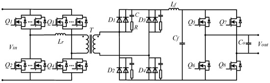
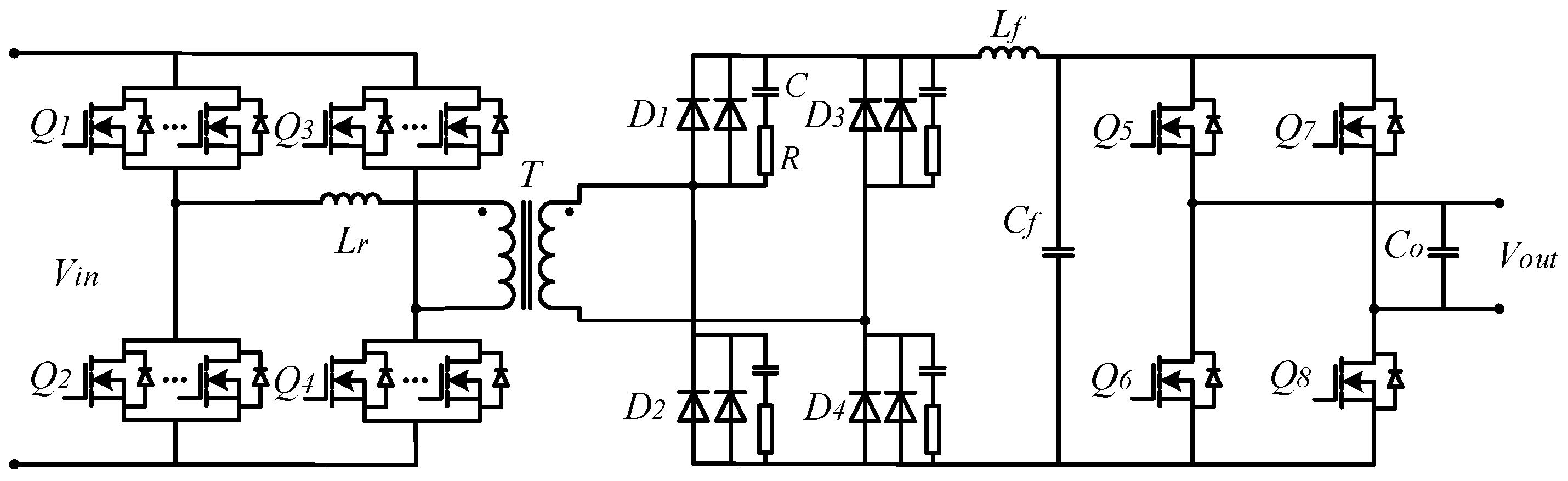
Figure 2 shows the PSFB-HFL inverter circuit topology based on the airborne application background. The main components consist of a PSFB circuit, an LC filter, and a subsequent full-bridge circuit. In the PSFB circuit, the four primary-side bridge arms Q1 to Q4 are connected in parallel using six switches each; the resonant inductor Lr is replaced by the transformer’s leakage inductance; the uncontrolled rectifier bridge diodes D1 to D4 are implemented as two parallel diodes; and the buffer circuit employs an RC snubber network. The LC filter comprises a filtering inductor Lf and a filtering capacitor Cf. The subsequent full-bridge circuit consists of switches Q5 to Q8, with Co serving as the output capacitor.
Figure 2.
PSFB-HFL inverter circuit.
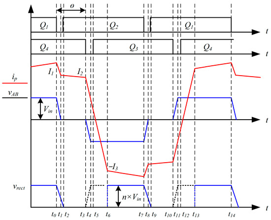
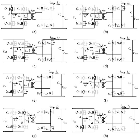
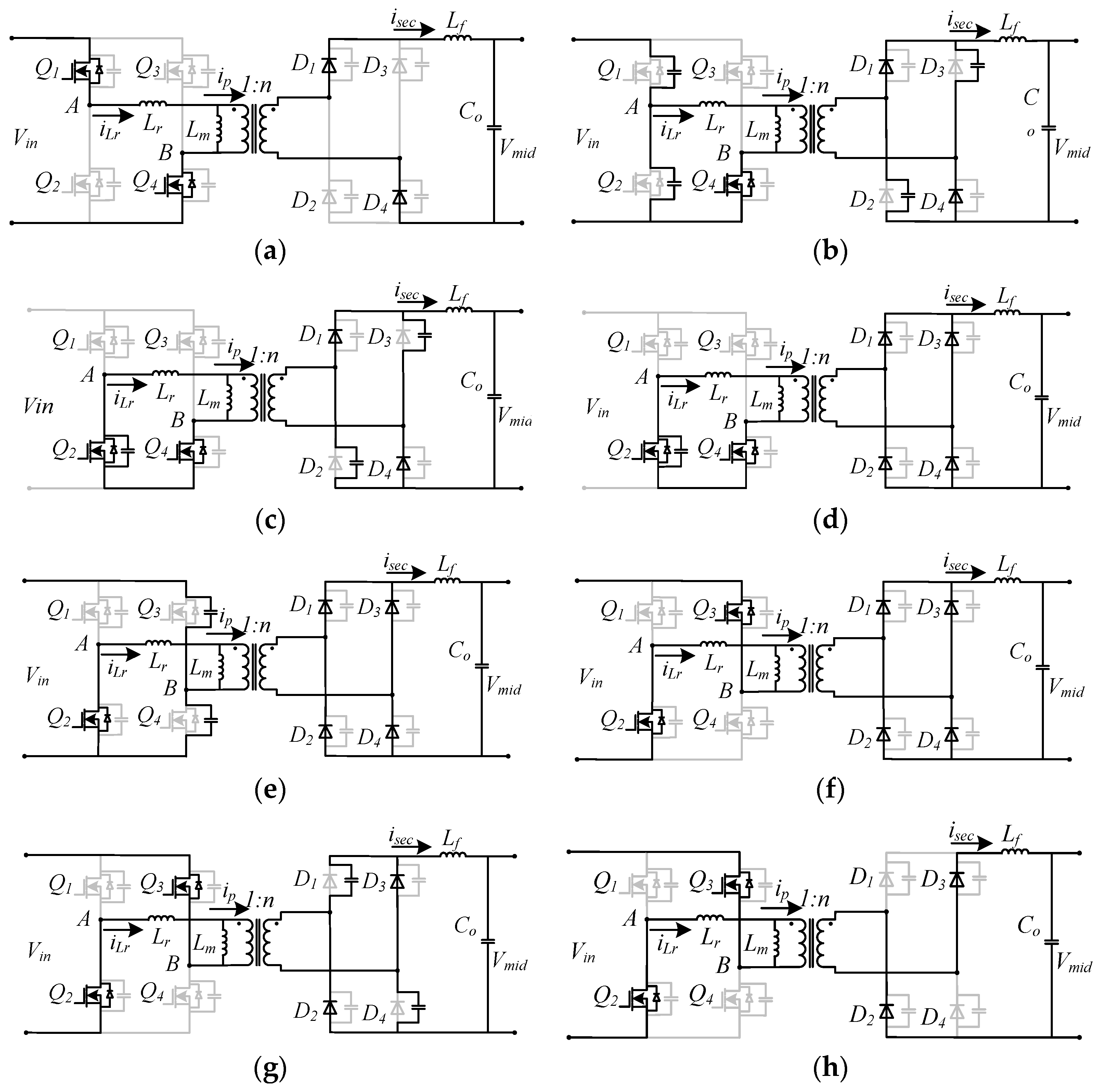
When analyzing the operation of the PSFB-HFL inverter, the following assumptions are made: (1) all components are regarded as ideal components; (2) the parasitic capacitances of the switches are equal; (3) , n is the voltage boost ratio. According to the working principle, for any one switching cycle, the working waveform of the pre-stage PSFB circuit is as shown in Figure 3, and all working states are as shown in Figure 4.
Figure 3.
Schematic diagram of the main waveforms of the single switching cycle of the PSFB circuit.
Figure 4.
Working states of the pre-stage PSFB. (a) During phase 0–t0; (b) during phase t0–t1; (c) during phase t1–t2; (d) during phase t2–t3; (e) during phase t3–t4; (f) during phase t4–t6; (g) during phase t6–t7; (h) during phase t7–t8.
Based on Figure 3 and Figure 4, the working states of the pre-stage PSFB circuit during each time interval are analyzed as follows:
[0~t0]: As shown in Figure 4a, switches Q1 and Q4 are conducting, and the resonant current iLr and the primary current ip both increase positively simultaneously. The primary and secondary windings of the transformer are coupled, and the rectifier diodes D1 and D4 are conducting, with energy being transmitted in the forward direction.
[t0~t1]: As shown in Figure 4b, Q1 is turned off, while the primary and secondary windings of the transformer remain coupled. The primary current ip gradually decreases due to the presence of the primary resonant inductor Lr and the secondary filter inductor Lf. At this time, the parasitic capacitance of Q1 charges, the parasitic capacitance of Q2 discharges, and the voltage potential at the midpoint A of the leading bridge arm drops. When Q1 is turned off, the voltage across the parasitic capacitance of Q1 changes little, and Q1 can be approximated as zero-voltage turn-off. At the same time, as the midpoint voltage vAB of the two bridge arms continuously decreases, the parasitic capacitance of D3 and D2 begins to discharge.
[t1~t2]: As shown in Figure 4c, the parasitic capacitance of Q2 discharges completely, and the body diode of Q2 continues to conduct. At this point, Q2 can achieve zero-voltage turn-on. For the boost scenario, the primary current of the transformer is large, and the capacitor discharges quickly, so when vAB is zero, the secondary voltage vrect still has a certain voltage, and the parasitic capacitances of D2 and D3 continue to discharge.
[t2~t3]: As shown in Figure 4d, vrect drops to zero, and the rectifier bridge diodes are all in the conducting state under the influence of Lf, which is called the short-circuit continuation state. During this state, there is no energy transfer between the primary and secondary sides of the transformer.
[t3~t4]: As shown in Figure 4e, Q4 turns off. Under the action of inductance Lr at the resonant point on the primary side, the parasitic capacitance of Q3 discharges, and the parasitic capacitance of Q4 charges. At the moment Q4 turns off, the voltage across the parasitic capacitance of Q4 changes little, and Q4 can be approximated as a zero-voltage turn-off.
[t4~t6]: As shown in Figure 4f, the parasitic capacitances of Q3 and Q4 are fully charged and discharged. The body diode of Q3 continues to conduct, and Q3 can achieve zero-voltage turn-on. During this period, the magnetic flux generated by the primary current is insufficient to couple the primary and secondary sides of the transformer, and there is no energy transfer. The secondary side of the transformer remains in the short-circuit continuation state. The primary current ip only decreases uniformly to zero and increases in the opposite direction under the action of Vin and Lr.
[t6~t7]: As shown in Figure 4g, when the primary current ip increases to enable energy transmission between the primary and secondary sides of the transformer, the parasitic capacitances of D1 and D4 start to charge until they are completely cut off.
[t7~t8]: As shown in Figure 4h, the working conditions of this state and the subsequent half-switching cycle are similar to those of the previous half-cycle. Therefore, no further elaboration is necessary.
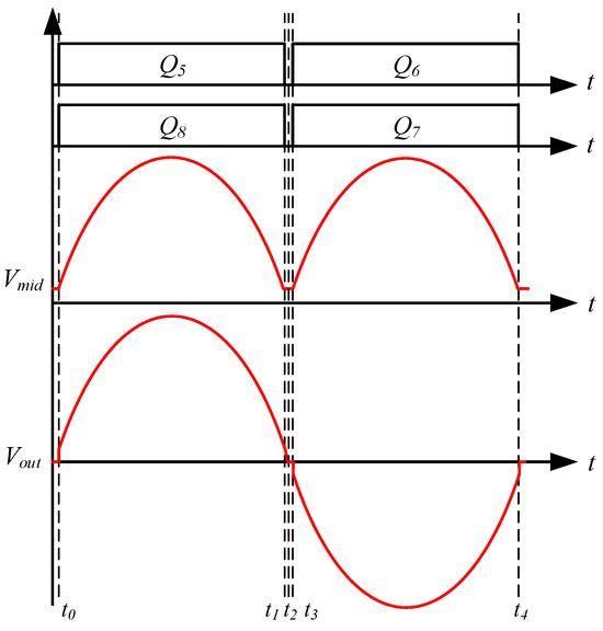
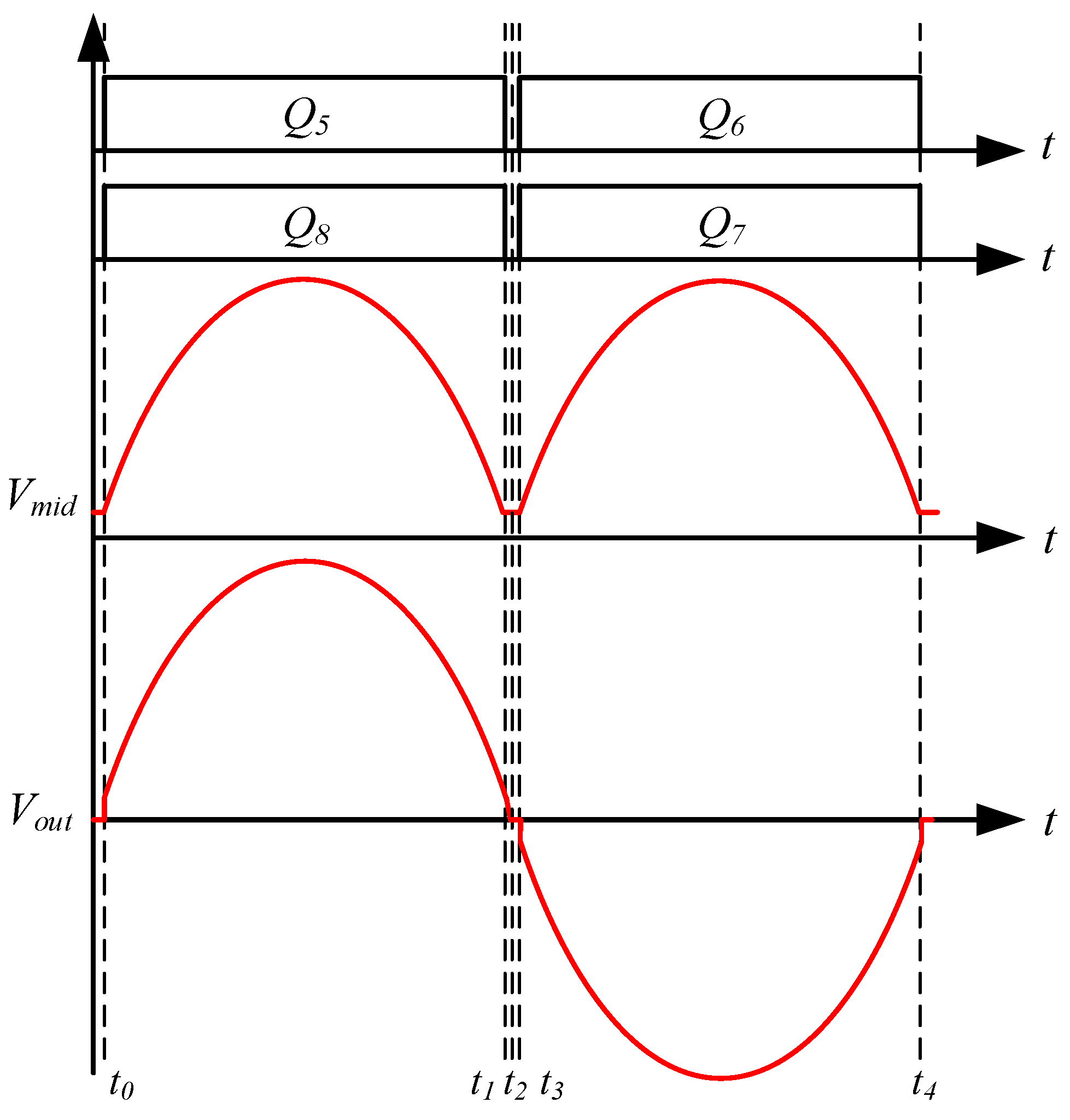
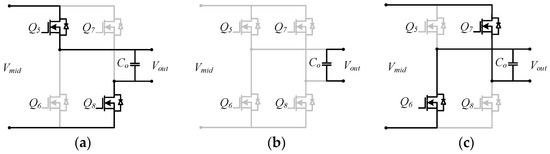
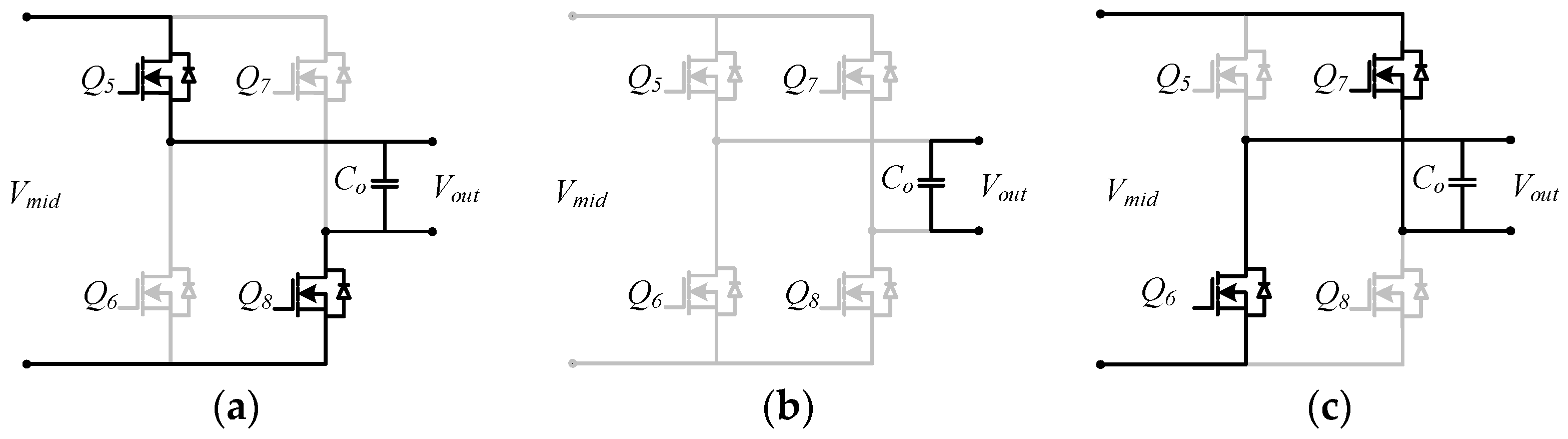
According to the PSFB-HFL working principle, after the pre-stage PSFB outputs a sinusoidal half-wave voltage, the post-stage full-bridge circuit then performs a corresponding inversion to output a sinusoidal wave. The main waveform diagram of the post-stage full-bridge circuit is shown in Figure 5, and the working process is depicted in Figure 6.
Figure 5.
Schematic diagram of the main waveforms of the post-stage full-bridge circuit.
Figure 6.
Working states of the post-stage full-bridge circuit. (a) During phase t0–t1; (b) during phase t1–t3; (c) during phase t3–t4.
The working states of the post-stage full-bridge circuit during each time interval are analyzed as follows:
[t0~t1]: As shown in Figure 6a, Q5 and Q8 are conducting, and the output of the positive half-wave Vmid is delivered to the load terminal.
[t1~t3]: As shown in Figure 6b, Q5 and Q8 are turned off, and the electrical energy on output capacitance Co continues to discharge until it becomes zero at t2. The design of Co aims to improve the sine waveform of the AC output.
[t3~t4]: As shown in Figure 6c, Q6 and Q7 are conducting, and the positive half-wave Vmid of the input is used to charge Co in reverse, and a reverse positive half-wave is output to the load terminal.
2.2. DC Bias Magnetic Field Problem and Consideration
The transformer in a bridge circuit operates in bidirectional magnetization mode. If this occurs, there may be a problem of DC bias magnetization. The specific phenomenon is that there is a difference in the volt-sec product of the positive and negative voltages of the transformer, causing the magnetic core’s hysteresis loop to no longer be symmetrical about the coordinate origin and thus causing the operating point to shift. In practical circuits, the causes may come from the following points: (1) differences in parasitic parameters of the switches or the driving circuit lead to inconsistent on–off conditions of each switch; (2) sudden changes in the load or interference to the circuit and the dynamic adjustment of the closed-loop system cause certain differences in the driving signal. When the DC bias magnetization is severe, it will cause distortion of the inductance current, increase the core loss, and subsequently lead to overcurrent, overheating and other problems. To ensure the reliable and normal operation of the PSFB circuit, the common methods for suppressing bias magnetization currently mainly include two aspects.
One approach is the hardware balancing method: for example, adding air gaps to the transformer to enhance its anti-polarizing magnetic capability and connecting a shunt capacitor in series in the primary circuit of the transformer. The design of the shunt capacitor method is simple. By utilizing the characteristic of capacitors to block direct current, it can effectively filter out the direct current components in the circuit. However, for the high voltage ratio and high power application scenarios studied in airborne application, the design parameters of the shunt capacitor are large, resulting in a larger overall volume of the power converter and introducing certain losses. At the same time, operating under high current will further reduce the service life of the electrolytic capacitor and decrease the reliability of the airborne equipment.
The other approach is algorithm control. The core idea of this method is to dynamically adjust the duty cycle and phase shift of the drive signal through closed-loop control, thereby quickly correcting the DC bias problem of the transformer. The existing solution can achieve this by designing a DC bias compensation unit, combining the three-phase shift modulation method of the dual active bridge DC–DC converter, using analog circuits to collect the DC bias current, and completing the suppression of the bias magnetic field through closed-loop duty cycle regulation. This idea can also be applied to the PSFB circuit. There is also a solution that uses peak current control to develop a prototype of the PSFB converter. Research on the single-stage bridge PFC topology indicates that, when the duty cycle of the primary voltage of the transformer changes according to the sine law, the center point of the magnetic core’s operation is most severely offset at 1/4 of the sine cycle. Based on this, a digital control method that ensures strict symmetry of the positive and negative half-cycles within a single switch cycle has been proposed.
The adoption of peak current mode control (PCMC) inherently mitigates transformer DC bias magnetization through its cycle-by-cycle flux balancing mechanism. In PCMC, the primary current is sensed and compared with a control reference on a per-switching-cycle basis. When a DC flux offset begins to accumulate due to volt-second asymmetry (e.g., from device mismatches or transient duty cycle variations), the resulting increase in the peak primary current of the affected half-cycle triggers earlier turn-off of the corresponding switch, thereby automatically reducing the volt-second product applied to the transformer in that half-cycle. This negative feedback action restores volt-second balance over successive cycles without requiring a DC-blocking capacitor or explicit leg-matching circuitry. It should be noted that this self-balancing capability is most effective under steady-state and moderate transient conditions. For severe transients or large parameter mismatches, additional measures such as dynamic duty cycle correction or a small blocking capacitor may be necessary to ensure robust operation. In the present design, the combination of PCMC with the proposed slope compensation scheme provides sufficient flux balancing for the intended operating range, as verified by the simulation waveforms presented in Section 3.5.
To clarify the selection rationale, the DC bias suppression methods discussed above can be compared from the following perspectives that are critical for aerospace applications. (1) Hardware balancing methods require additional passive components (air gaps, capacitors) and increase circuit complexity. Algorithm control methods, including DC bias compensation units and three-phase shift modulation, require dedicated DSP-based digital implementation with complex closed-loop control algorithms and dedicated DC bias sensing circuits. Peak current control, while also implemented on a DSP, involves relatively simpler control logic as it primarily relies on the inherent characteristics of the current inner loop. (2) Hardware methods provide passive suppression but may degrade under extreme operating conditions and introduce additional loss mechanisms. Algorithm control methods can achieve high suppression accuracy but depend on the reliability of sensing circuits and digital control loops. Peak current control, when combined with slope compensation (as discussed in Section 3.1), provides effective suppression of sub-harmonic oscillations and offers inherent peak current limiting, which is particularly valuable for aerospace applications where overcurrent protection is critical for system reliability.
Considering the above factors, particularly the aerospace requirements for high reliability, fast dynamic response, and the need for accurate small-signal modeling of the current inner loop, this project selects the peak current control scheme. It should be noted that the selection of peak current control is also motivated by the fact that the core contribution of this paper is the accurate small-signal modeling of the peak current inner loop for PSFB-HFL inverters, and the chosen control scheme directly enables this modeling contribution. The sub-harmonic oscillation issue inherent to peak current control at duty cycles greater than 50% is addressed through slope compensation, as detailed in Section 3.1.
3. The Control Strategy of the PSFB-HFL Inverter
3.1. Sub-Harmonic Oscillation and Slope Compensation
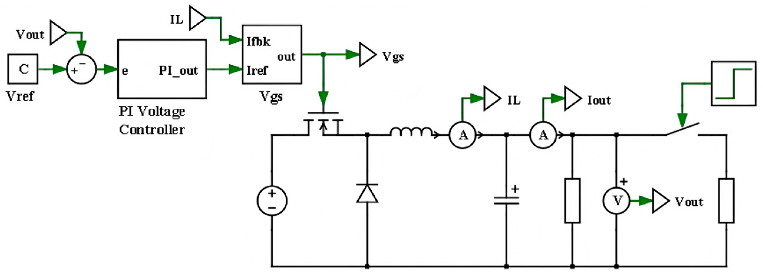
To address the problem of DC biasing in transformers, the peak current control strategy is adopted. Moreover, peak current control has the advantages of current limiting and fast dynamic response. However, peak current control also has the problem of sub-harmonic oscillation. It can make the output unstable; the system’s anti-interference ability weakens, and its electromagnetic compatibility deteriorates. The common solution is to add a slope compensation to the current reference value. For a simple Buck circuit model, the sub-harmonic generation causes, its hazards, and the effect after adding the slope compensation are better described through PLECS simulation. As shown in Figure 7, the output voltage Vout is the voltage outer-loop feedback quantity, and the inductor current IL is the peak current inner loop feedback quantity.
Figure 7.
Buck converter model diagram.
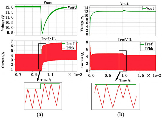
The generation of sub-harmonics is caused by a duty cycle greater than 50%. The specific phenomenon is shown in Figure 8. Figure 8a,b show the relationship graphs of peak current reference value Iref, current feedback value Ifbk, and drive signal Vgs when the duty cycle is less than 50% and greater than 50% respectively without slope compensation. After the system stabilizes, the duty cycle of the drive signal is one large and one small, with a frequency of half of the switching cycle, which is called sub-harmonic oscillation.
Figure 8.
Schematic diagram of sub-harmonic oscillation. (a) Duty cycle is less than 50%; (b) duty cycle greater than 50%. Simulation parameters: Vin = 12 V, L = 60 μH, C = 100 μF, fs = 50 kHz. Note that the Buck-based simulation in this subsection is only used to illustrate the sub-harmonic oscillation mechanism by analogy and does not represent the full PSFB-HFL inverter. The parameters of the complete prototype are given in Table 1.
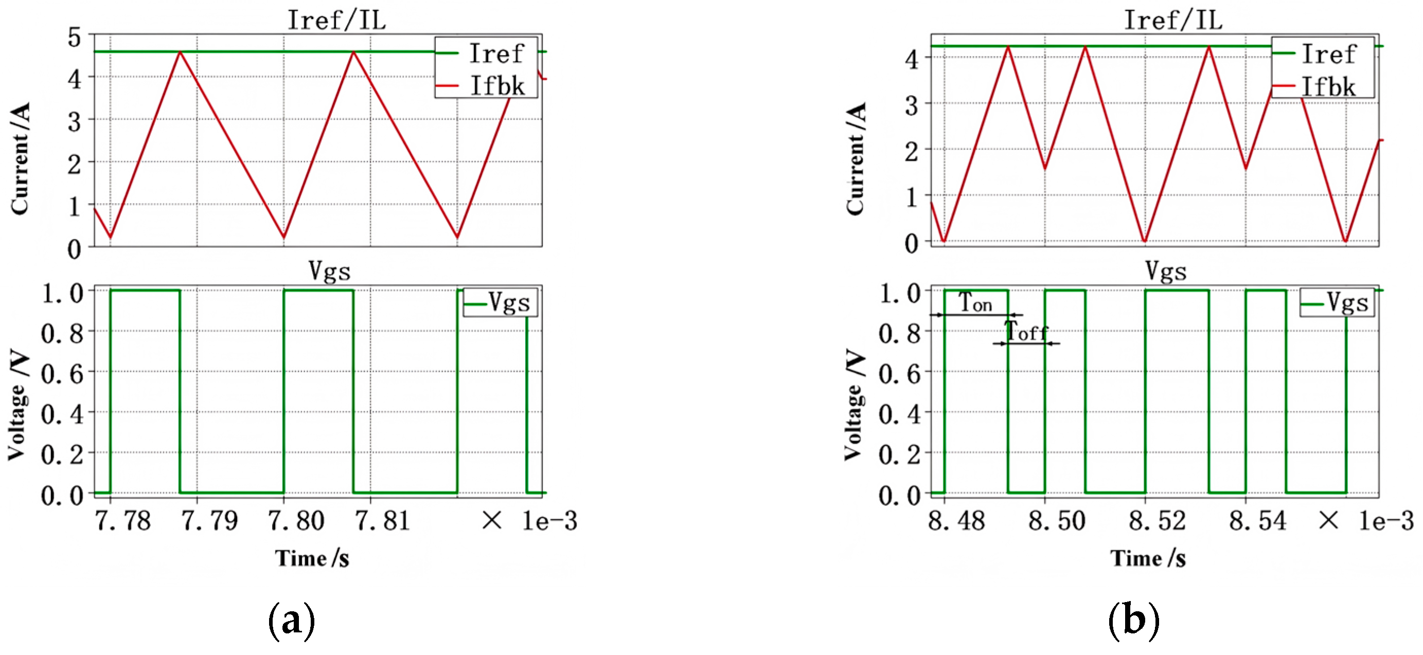
Table 1.
List of key parameters used for the small-signal model derivation and the compensated Bode plot.
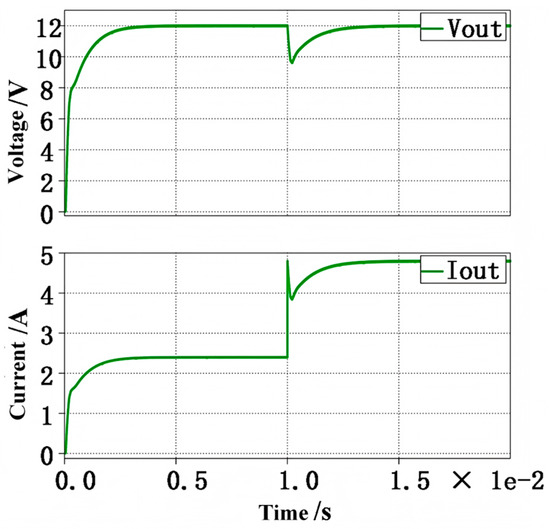
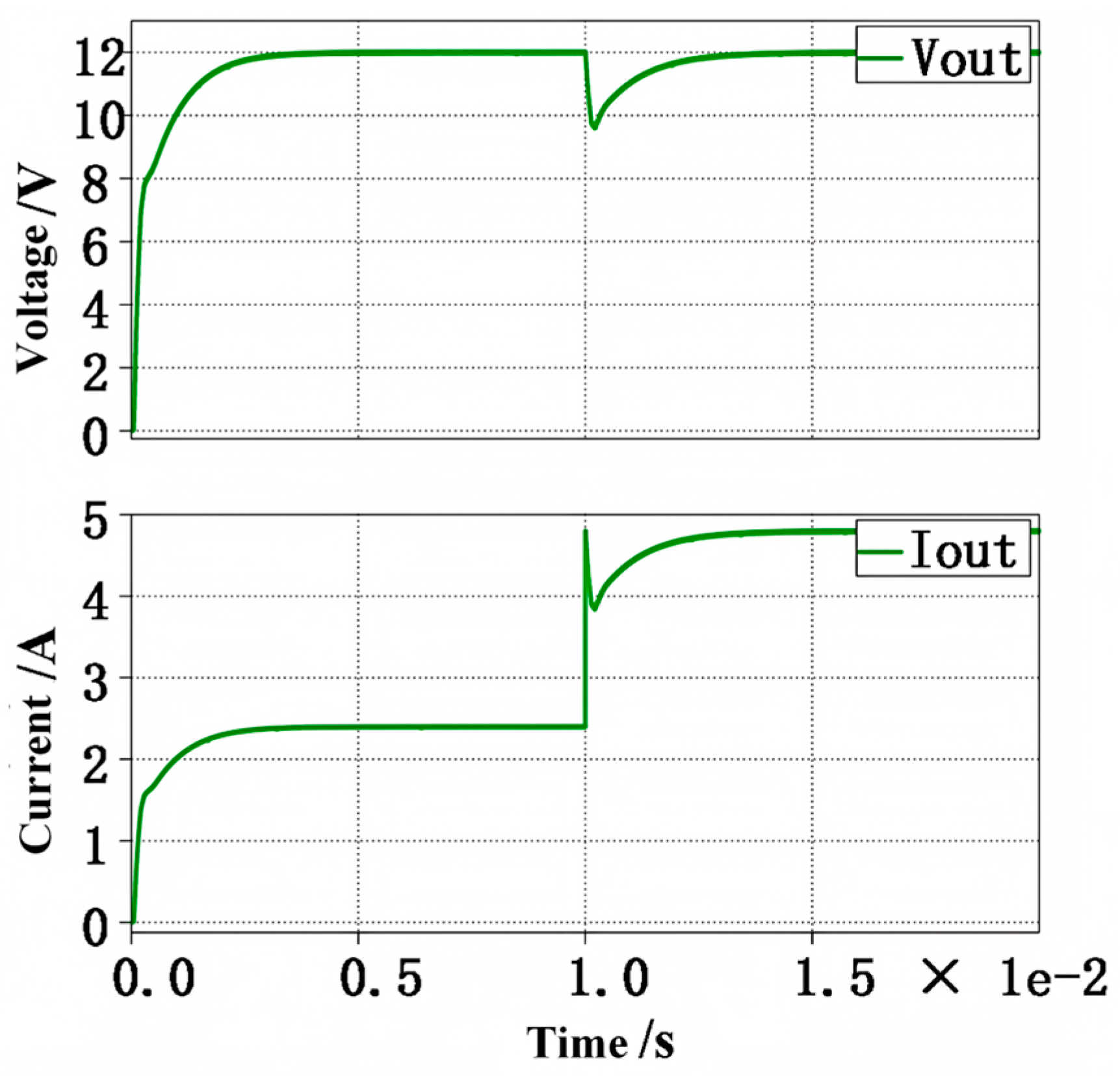
Closed-loop control with low-voltage input or high power output can cause the duty cycle to be greater than 50%, thereby causing sub-harmonic oscillation. However, even when the duty cycle of closed-loop control is less than 50%, a sudden drop in input voltage will also cause sub-harmonic resonance. The specific reason is, in a simple Buck converter model, the slope of the inductor current is only related to the input voltage and the size of the filter inductor; when the input voltage drops, the slope of the inductor current decreases, and the peak current reference value fails to respond in time. If the on-duty cycle is greater than 50%, the output load current (average current) increases, the output voltage increases, and at this time, sub-harmonic oscillation will also form. Similarly, when a load is suddenly added, after voltage outer-loop regulation, the output peak current reference value will also increase. If the duty cycle is greater than 50%, sub-harmonic oscillation will also form for a period of time, as shown in Figure 9.
Figure 9.
Analysis diagram of the causes of sub-harmonic oscillation. (a) Sudden drop in input voltage; (b) sudden increase in load.
Therefore, to suppress the sub-harmonic oscillations, slope compensation is always added to the peak current control. By incorporating an appropriate slope compensation, regardless of factors such as duty cycle greater than 50%, input voltage jitter, sudden addition or removal of the output load, and current perturbations, the system will not generate sub-harmonic oscillations, and the interference signals will converge, significantly improving the stability of the system.
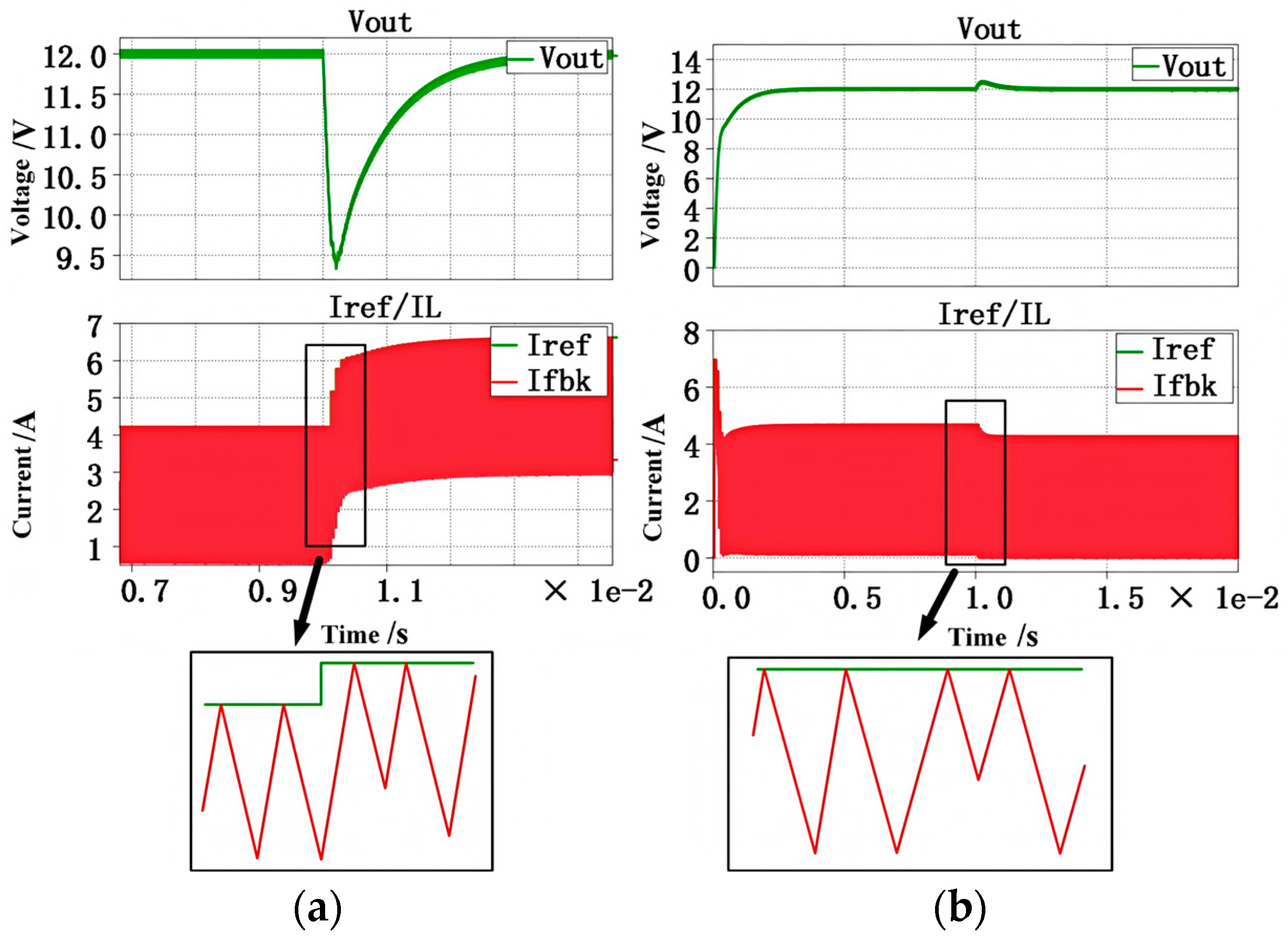
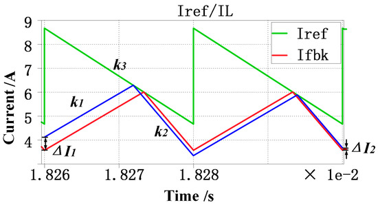
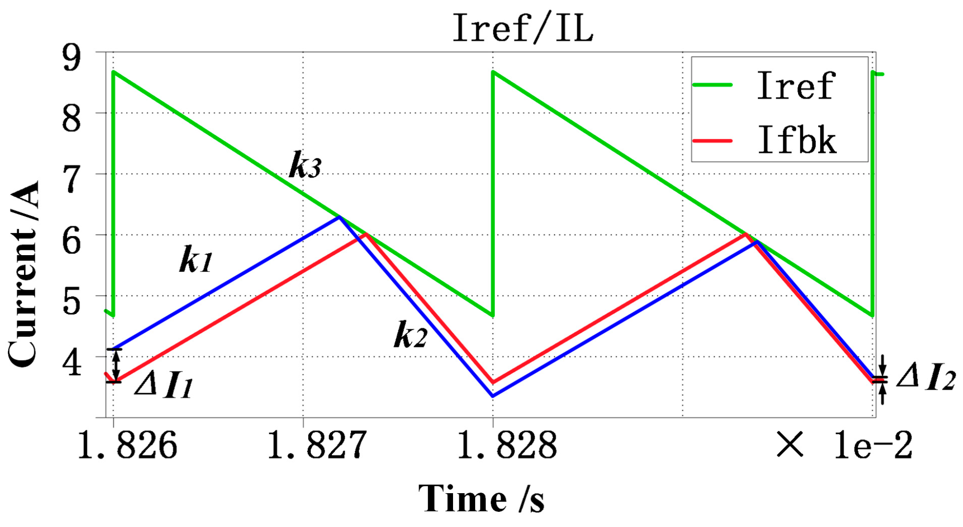
As shown in Figure 10, after adding the slope compensation, even when the duty cycle is greater than 50%, the system output waveform is stable. As shown in Figure 11, the red line represents the inductor current waveform when the duty cycle is greater than 50%, and it can remain stable. At this time, if an inductor current perturbation of size ΔI1 is introduced, the inductor current becomes the blue line. Through the geometric relationship in the figure, it can be known that ΔI2 < ΔI1, and the current perturbation converges, having no impact on the system. Let the ramp of the slope function be k3, the slope of the inductor current rise be k1, and the slope of the inductor current drop be k2. The following equation relationship can be obtained:
Figure 10.
Slope compensation effect diagram.
Figure 11.
Slope compensation principle diagram.
Therefore, k3 > k2/2. As long as the ramp of the slope compensation is set reasonably, the system can remain stable.
To clearly define the stability assessment criteria adopted in this paper, two distinct types of stability are considered: (1) Small-signal stability: This refers to the stability of the peak current inner loop against sub-harmonic oscillations. The stability criterion is based on the convergence of current perturbations across switching cycles. Specifically, if a perturbation ΔIn is introduced to the peak inductor current at the n-th switching cycle, the system is small-signal stable if and only if ΔIn+1 < ΔIn, and the perturbation monotonically decreases from cycle to cycle. With proper slope compensation (k > kcritical), this condition is satisfied, and sub-harmonic oscillations are suppressed, as demonstrated in Section 3.1. (2) Large-signal dynamic stability: This refers to the ability of the output voltage to recover to its steady-state value after a large-signal disturbance, such as a step load change.
In the following analysis and experiments, stability claims are specified according to the above definitions. The small-signal stability is verified through the perturbation convergence analysis in Section 3.1 and the slope compensation simulation in Section 3.2, while the large-signal dynamic stability is evaluated through the load transient experiment in Section 4.3.
3.2. Peak Current Control Implementation of the PSFB Circuit
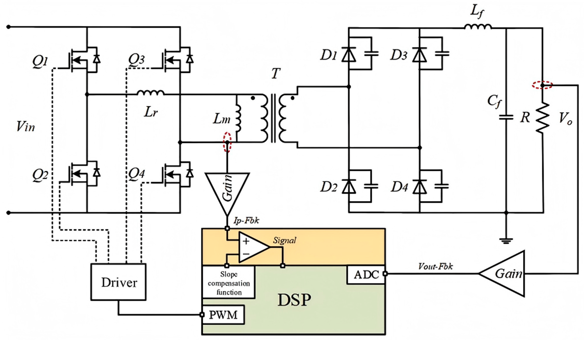
The key to realizing the functions of the PSFB-HFL inverter lies in the PSFB closed-loop output of the sinusoidal half-wave. This section mainly focuses on the peak current control of the PSFB circuit to achieve the DC-sinusoidal half-wave transformation. As shown in Figure 12, the control block diagram of the peak current control PSFB converter is presented. It uses a digital signal processor (DSP), with the yellow part being the internal analog circuit of the chip and the green part being the software controller. The specific implementation is as follows. The output voltage sampling is processed by the external analog circuit and sent to the DSP. The digital controller realizes the voltage outer-loop control and outputs the peak current reference value. The sampling point of the primary current of the PSFB converter can be the primary side of the transformer or the bus after the input filter capacitor. A sampling point for the primary current on the primary side of the transformer is designed, which is processed by the external analog circuit and sent to the DSP, connected to the in-phase terminal of the comparator inside the DSP, and the peak current reference value generated by the voltage outer loop is sent to the opposite terminal of the comparator after being configured by the software-specified slope compensation function. The internal analog comparator can be used to achieve a rapid response for peak current control. The output signal is processed by digital interrupt, configured with the PWM module, and the output signal causes the switching tubes of the PSFB converter to act immediately.
Figure 12.
Control block diagram of PSFB converter with peak current control.
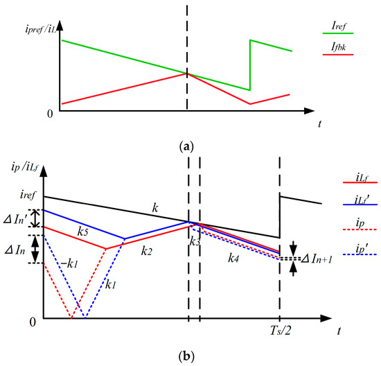
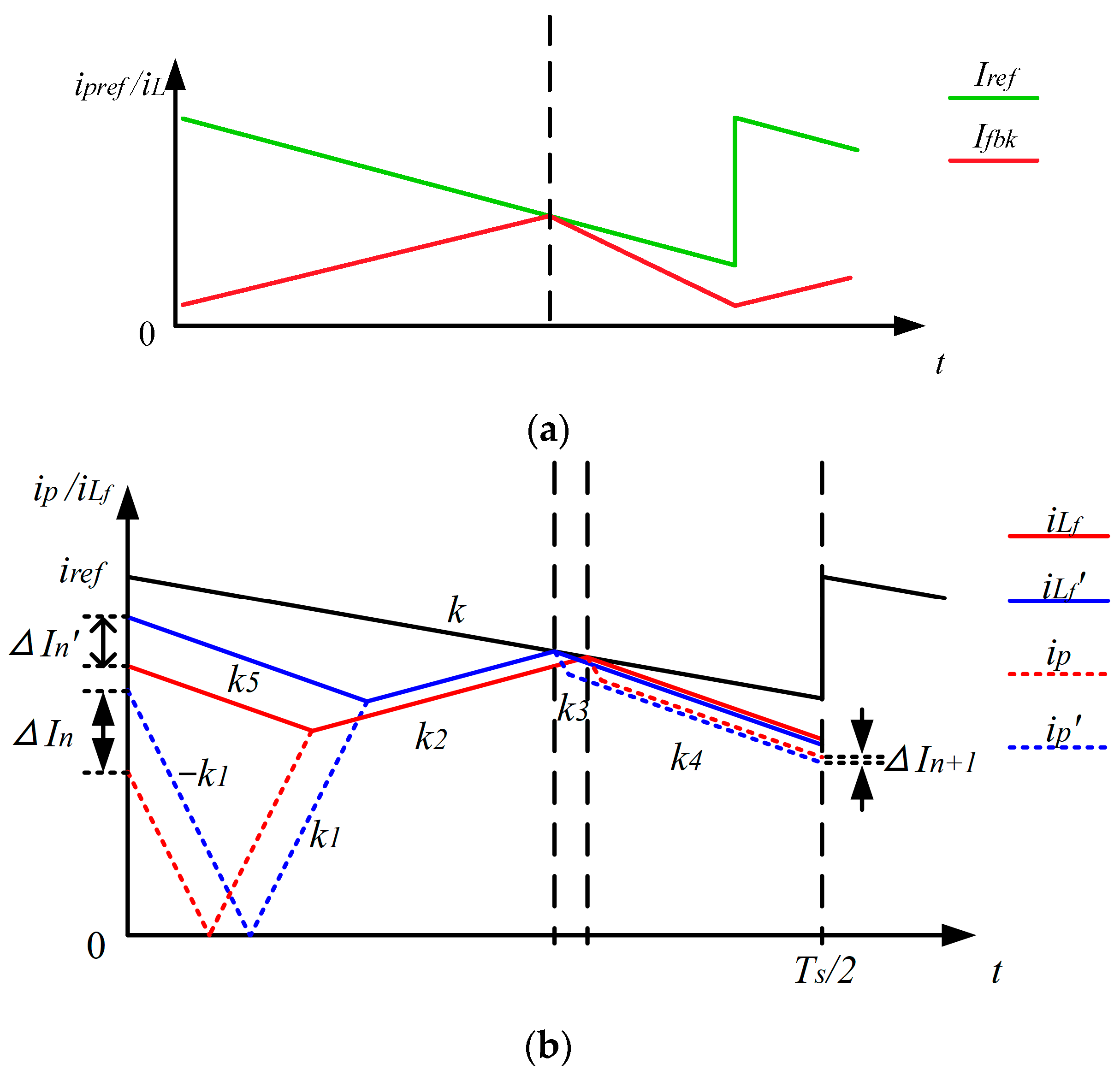
In Section 3.1, based on the principle and existing problems of peak current control in the Buck circuit, as well as the effect of slope compensation, a detailed analysis and simulation verification were conducted. The PSFB circuit part of the PSFB-HFL inverter is also a type of Buck circuit. Figure 13a,b show the main waveform diagrams of peak current control for the Buck circuit and the PSFB circuit respectively. For the Buck circuit, the conduction time of the switch corresponds to the time when the diagonal switches of the PSFB circuit are conducting and overlapping and transferring energy, further demonstrating the similarity between the two. Therefore, based on the above conclusions obtained, in the PSFB circuit, the peak current control analysis is directly carried out by analogy with the Buck circuit.
Figure 13.
Peak current control principle diagram. (a) Schematic diagram of the main waveform for peak current control of the Buck circuit; (b) main waveform diagram of peak current control for PSFB circuit.
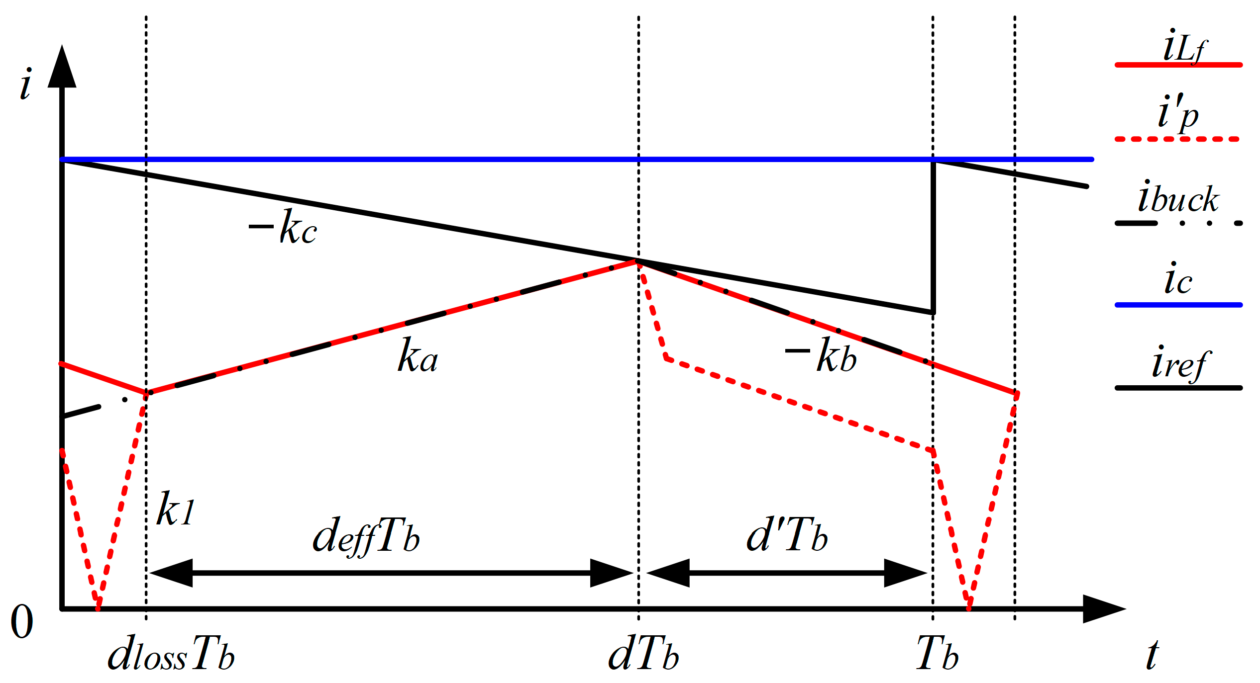
As shown in Figure 13b, k to k5 represent the slopes of each straight line, iref is the peak current reference value provided by the voltage outer loop to the inner loop, and the red solid line and the red dashed line represent the filtered inductor current iLf and the primary current ip respectively under normal conditions, while the blue solid line and the blue dashed line represent the filtered inductor current iLf′ and the primary current ip′ after being disturbed. To make the schematic diagram more intuitive, the filtered inductor current in the figure has been amplified by the boost ratio n. From Figure 13b, it can be seen that, after adding slope compensation to the primary peak current control, when the duty cycle is greater than 50%, even if an external disturbance ΔIn is introduced, it can converge after one cycle, proving that the small-signal stability criterion is satisfied and the peak current inner loop operates without sub-harmonic oscillation. Further, the relationships in the figure are listed as the following equation relationships for analysis. By setting the slope compensation factor k to k4, it is possible to ensure that ΔIn+1 < ΔIn.
3.3. Small-Signal Modeling of PSFB Circuit
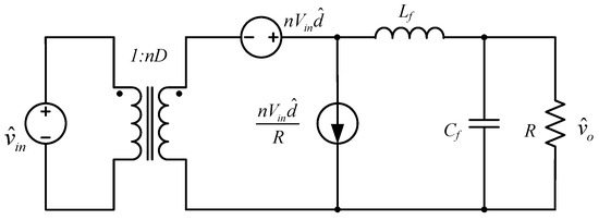
The PSFB converter belongs to the Buck-type converter. Therefore, the analysis of the small-signal model of the PSFB circuit is based on the Buck circuit. As shown in Figure 14, it is the small-signal model of the Buck circuit.
Figure 14.
Small-signal model of the Buck circuit.
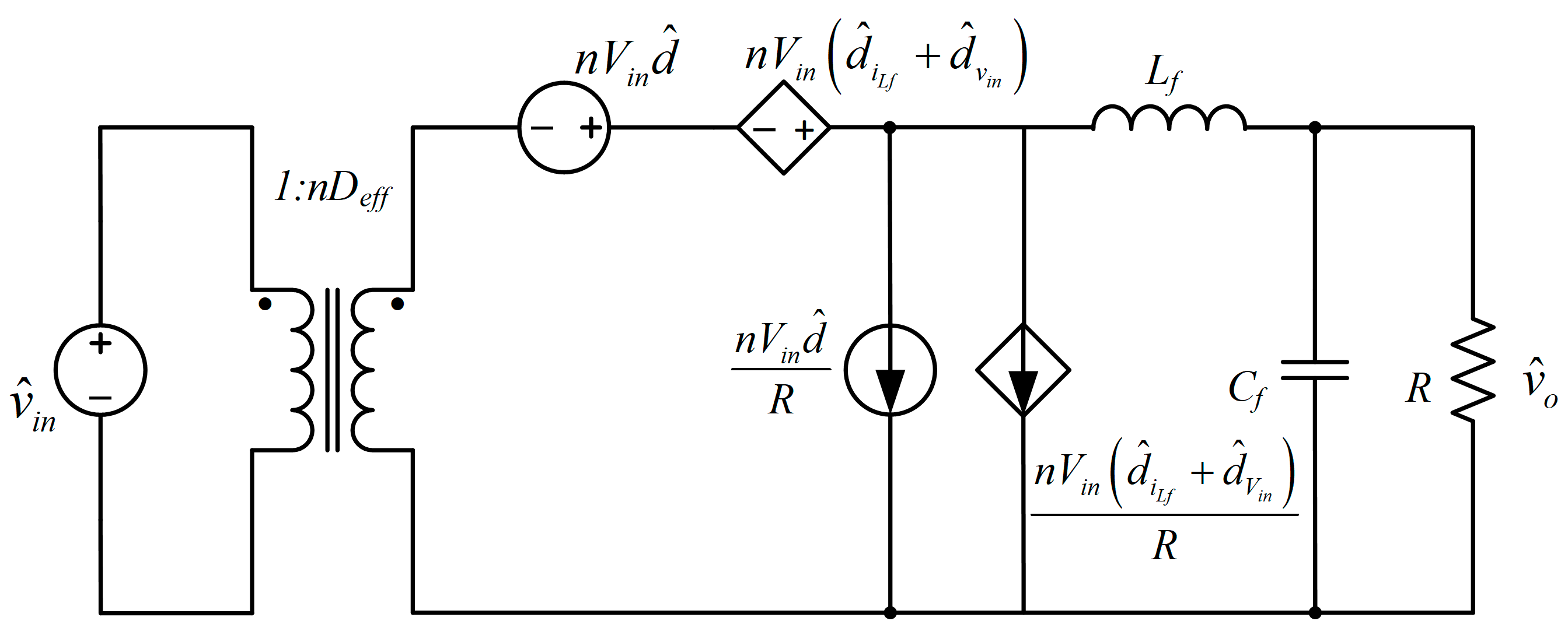
Based on the Buck circuit, the PSFB circuit needs to take into account the loss of duty cycle. Considering the situation where there is ripple in the inductor current in practice, the following equation relationship can be obtained:
In the above equation, the variables are the switching period Ts, the duty cycle of the primary side of the transformer D, and the effective duty cycle Deff of the secondary side. Generally, after the circuit parameters are designed, the main consideration is the influence of D, Vin, and ILf perturbations on the effective duty cycle. Therefore, by adding the corresponding perturbations to the effective duty cycle, the following equation relationship can be obtained:
After sorting out, the following expression was obtained:
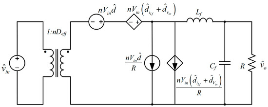
In the formula, RZ = 4n2Lrfs. The variables are the duty cycle perturbation caused by itself, the duty cycle perturbation caused by Vin perturbation, the duty cycle perturbation caused by iLf perturbation, and the duty cycle perturbation of the effective duty cycle on the secondary side. Therefore, based on the relationship of the above Equation (6), the small-signal model of the PSFB converter is obtained on the basis of the small-signal model of the Buck circuit, as shown in Figure 15.
Figure 15.
Small-signal model of the PSFB circuit.
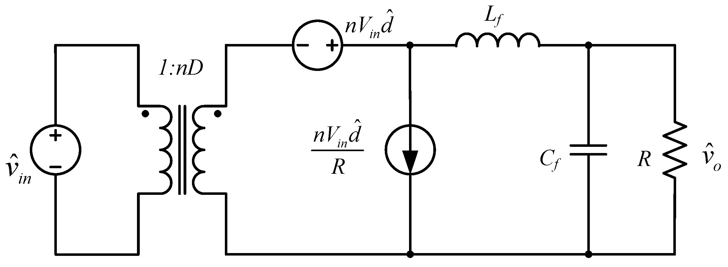
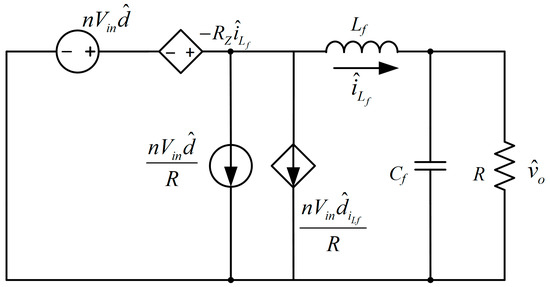
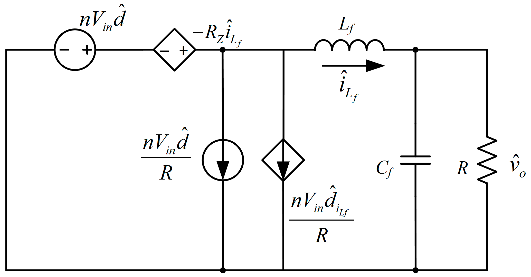
To prepare for the analysis of the peak current control loop model, this subsection needs to obtain the transfer functions Gvd(s) and Gid(s) of duty cycle perturbation to output voltage and inductor current separately based on the small-signal model of the PSFB converter. If the input voltage perturbation is not considered, combine Equation (6) and simplify the small-signal model of the PSFB converter, as shown in Figure 16.
Figure 16.
The small-signal model of PSFB that only considers the duty cycle perturbation.
The output impedance is defined, and the following equation relationship is obtained:
After sorting out, we can conclude that:
3.4. Small-Signal Model of Peak Current Control Based on the Average Value of iLf
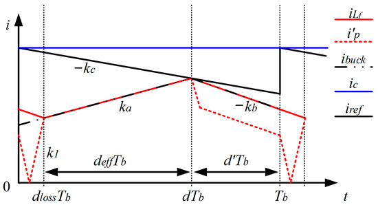
In order to establish a small-signal model of the peak current control loop for the PSFB circuit, the key waveforms of the PSFB converter need to be simplified first. The primary current ip can be equivalently transformed to the secondary side of the transformer, that is, it is reduced by a factor of n to become i′p. The complex actual waveform of i′p can be replaced by the current iLf of the filter inductor on the secondary side of the transformer, and the influence of dloss is temporarily ignored. Thus, the key waveforms of the Buck circuit are shown in Figure 17. The on-time of the switch in the Buck circuit is dTb, the off-time is d′Tb, the rising slope of the inductor current ibuck is ka, the falling slope is −kb, and the period Tb is 1/2 of Ts. After slope compensation of the control current ic, the reference current iref is obtained, with a slope of −kc.
Figure 17.
The simplified PSFB circuit is equivalent to the key waveform diagram of the Buck circuit.
From Figure 16, we can obtain the average value of the inductor current in the Buck circuit:
Introduce small-signal perturbations in the above variables: the average value of ibuck period ; the average value of ic period ; the duty cycle d, ka, and kb while keeping the slope compensation of iref unchanged. The following equation relationship is obtained:
By omitting the lower-order terms and retaining only the first-order terms, we can obtain:
Furthermore, based on the following equation relationships existing in the Buck circuit:
The final duty cycle perturbation of the Buck circuit can be obtained as:
According to the waveform relationship shown in Figure 17, the assumption for the validity of the above equation is that the current iLf of the filter inductor on the secondary side of the PSFB circuit is equal to the current ibuck of the inductor in the Buck circuit. To convert iLf back to the primary current ip of the PSFB circuit, it is necessary to take into account the specific duty cycle loss and transformer step-up ratio n of the PSFB circuit. Based on Equation (16), the specific variable substitution relationship is:
Meanwhile, if the issue of the proportion scaling of the primary current sampling in the actual circuit is not taken into consideration, a small-signal model of PSFB based on the filtered inductor current and using peak current control can be obtained. The effective duty cycle perturbation of the PSFB circuit can be derived from Equations (16) and (17):
Simplified as:
In the equation:
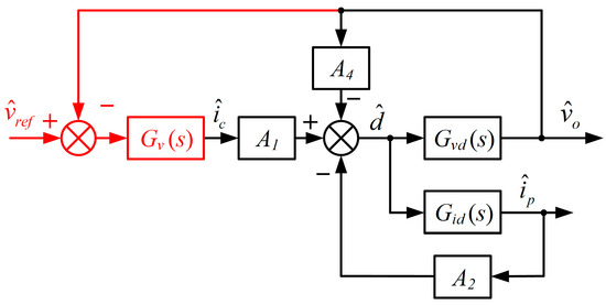
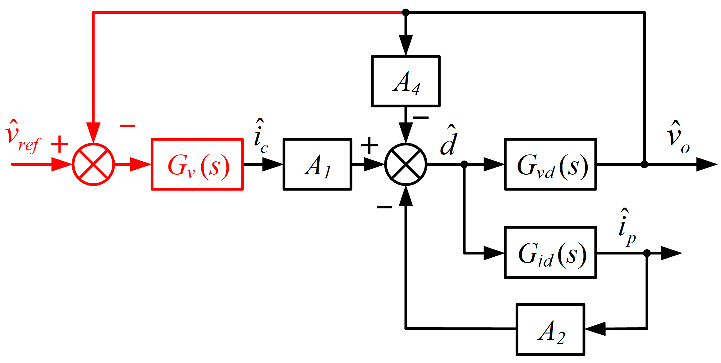
Without considering the input voltage disturbance, by designing another voltage outer-loop controller Gv(s), the peak current control PSFB voltage outer-loop control block diagram as shown in Figure 18 can be obtained.
Figure 18.
Peak current control PSFB voltage outer-loop control block diagram.
The transfer functions Gvi(s) for controlling the current to the output voltage and Gvr(s) for the reference voltage to the output voltage are respectively:
To achieve stable output of the system and enhance its dynamic performance, a PI compensator is selected for the closed-loop design of the system. The expression of Gv(s) is as follows:
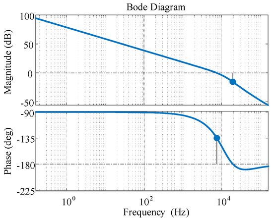
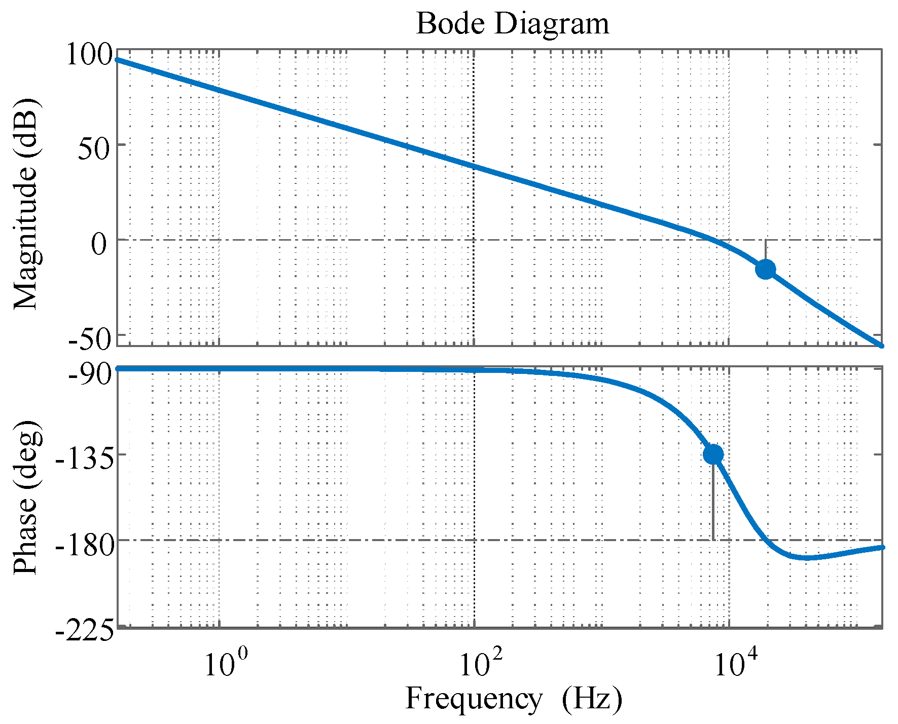
To achieve stable output of the system and improve its dynamic performance, in practical engineering applications, the phase margin is generally designed to be between 40° and 60°, and the amplitude margin is between 10 dB and 20 dB. Combining the previous results to obtain the transfer functions of the controlled object and the controller, substitute the actual circuit parameters, and draw the open-loop Bode plot of the system after compensation in MATLAB 2022b, as shown in Figure 19. The key parameters used for the small-signal model derivation and the compensated Bode plot (Figure 19) are listed in Table 1. It can be seen that the system’s cutoff frequency is 7.5 kHz, the phase margin is 45°, and the amplitude margin is 15.5 dB, which meets the system design requirements.
Figure 19.
The open-loop Bode plot of the system with compensation added.
3.5. Implementation of DC Bias Suppression
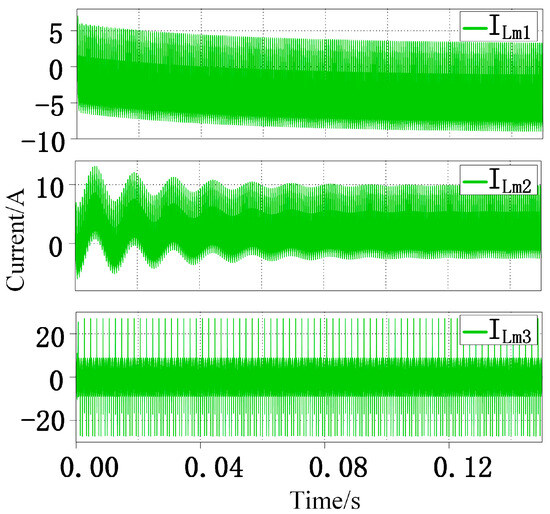
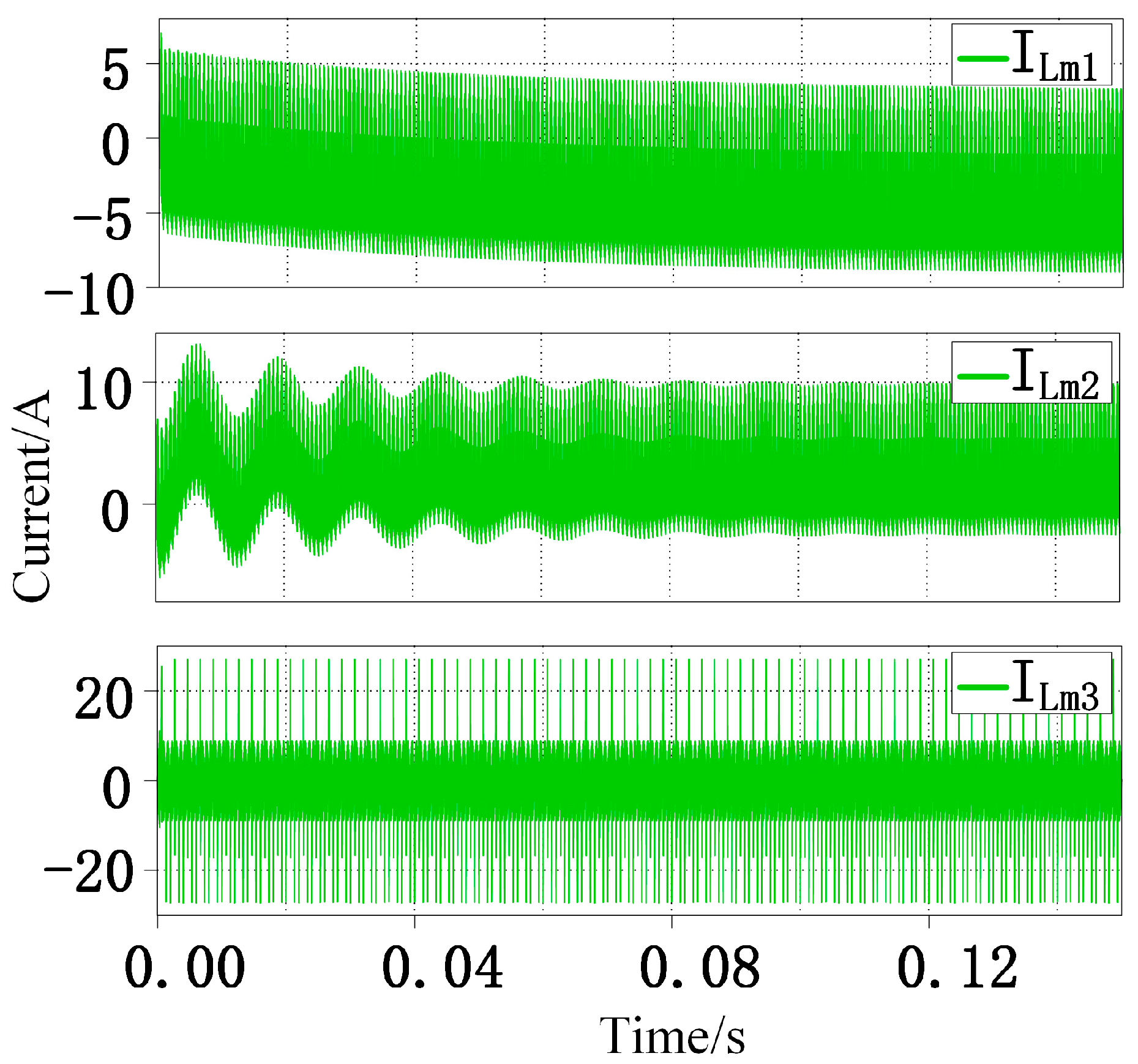
To further verify the effectiveness of the proposed PCMC strategy in suppressing DC bias, a comparative simulation is conducted. Volt-second imbalance is intentionally induced by extending the dead-time of switches Q1 and Q4. Three control strategies are compared: (i) conventional phase-shift control without PCMC, (ii) phase-shift control combined with a DC-blocking capacitor, and (iii) the proposed PCMC strategy without a DC-blocking capacitor. The corresponding transformer magnetizing current ILm waveforms are presented in Figure 20. As observed in Figure 20, when employing conventional phase-shift control, the magnetizing current drifts gradually over successive cycles, exhibiting a slowly diverging DC bias even after reaching steady state. When a DC-blocking capacitor is added, the magnetizing current envelope exhibits initial oscillations before stabilizing. In contrast, under the proposed PCMC strategy, the magnetizing current reaches a stable state in the shortest time.
Figure 20.
Magnetizing current ILm waveforms.
Furthermore, by calculating the average value of the primary current, the following behaviors are identified: under conventional phase-shift control, the DC bias current continues to diverge slowly even in the steady state. In contrast, under the proposed PCMC strategy, the DC bias current remains stable within a negligible range (0 to 0.2 A). The addition of a DC-blocking capacitor provides the best suppression effect, where the primary current exhibits almost no DC offset.
Synthesizing these results, the proposed PCMC strategy demonstrates excellent performance in DC bias suppression with fast dynamic response, effectively maintaining the magnetizing current within a safe and negligible DC offset range (0–0.2 A) for the intended operating conditions.
4. Experimental Verification
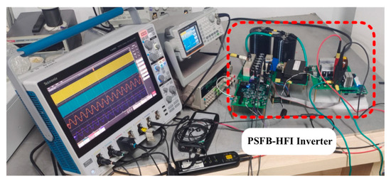
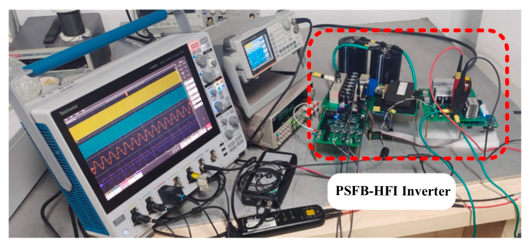
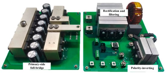
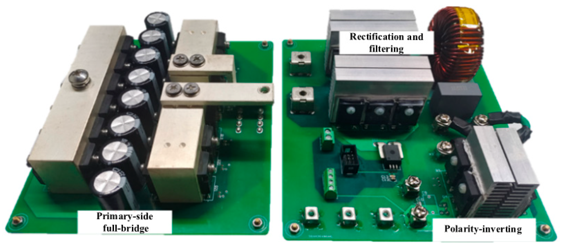
The prototype of the PSFB-HFL inverter and the experimental platform were constructed as shown in Figure 21. The PSFB-HFL inverter consists of a primary-side full-bridge power board, secondary-side rectification and filtering unit, a sine half-wave polarity-inverting power board on the secondary side, along with front-end and rear-end driver boards and a control board. To reduce input DC voltage ripple, a large capacitor bank is connected in parallel at the input of the single-phase PSFB-HFL inverter. The picture of the inverter is shown in Figure 22.
Figure 21.
PSFB-HFL inverter prototype and experimental platform.
Figure 22.
Main power board with primary-side full-bridge, rectification and filtering unit and polarity inverting.
The key experimental parameters and equipment are summarized in Table 2. All experimental waveforms presented in this section were captured using a high-bandwidth oscilloscope (Tektronix MSO46) with isolated probes.
Table 2.
List of key experimental parameters and equipment.
4.1. ZVS Experiment
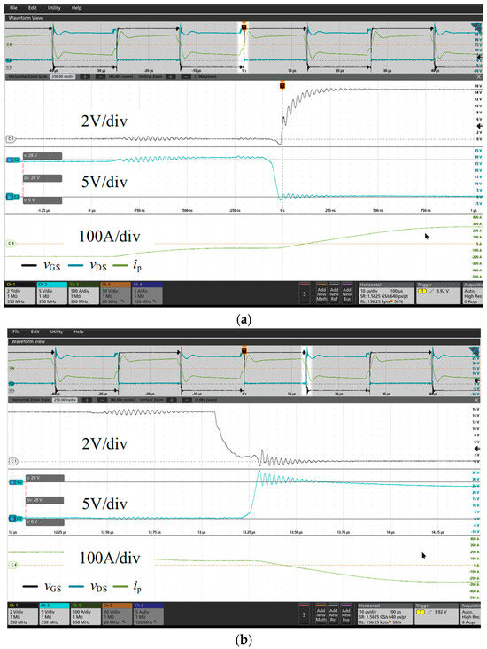
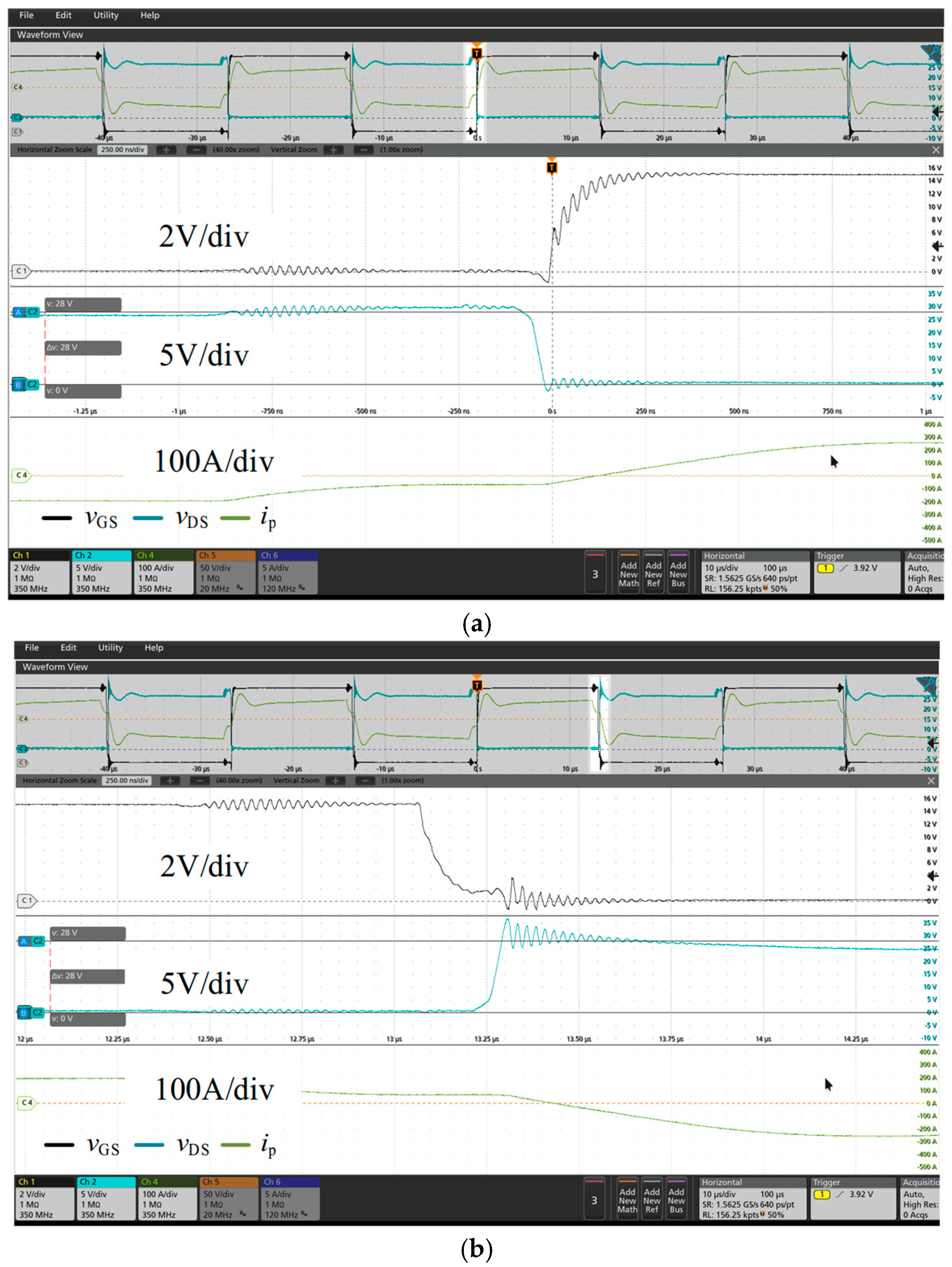
During the experimental process of the PSFB-HFL inverter function implementation, the pre-stage PSFB circuit was first tested to verify the ZVS performance of the prototype hardware design. The experimental conditions were an open-loop DC–DC conversion of the pre-stage PSFB circuit, with an input of 28 V DC, a fixed duty cycle of 93.75%, and an output power of 4 kW.
The soft-switching experimental results of the lagging bridge arm switches are shown in Figure 23. Figure 23a is the turn-on diagram of the switch, and Figure 23b is the turn-off diagram of the switch. Channel 1 is the gate-source voltage vGS, channel 2 is the drain-source voltage vDS, and channel 4 is the primary-side current ip. From Figure 23, it can be seen that the lagging bridge arm achieved zero-voltage turn-on and turn-off, which is consistent with the principle analysis in Section 2.1. At the same time, the lagging bridge arm achieved ZVS, which also proves that all the switches in the primary-side full-bridge of the PSFB converter can achieve ZVS.
Figure 23.
ZVS waveforms of the lagging bridge arm in pre-stage PSFB circuit. (a) Turn-on diagram of the switch; (b) turn-off diagram of the switch.
To further clarify the ZVS performance across the load range, the ZVS capability of both the leading-arm and lagging-arm switches is discussed below. In the PSFB-HFL inverter, the leading-arm switches benefit from the resonant current and the magnetizing current, which together provide sufficient energy to charge and discharge the output capacitances of the MOSFETs during the dead-time interval. As a result, the leading-arm switches can maintain ZVS over a wide load range, typically from approximately 25% to 100% of full load.
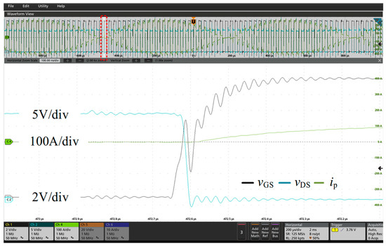
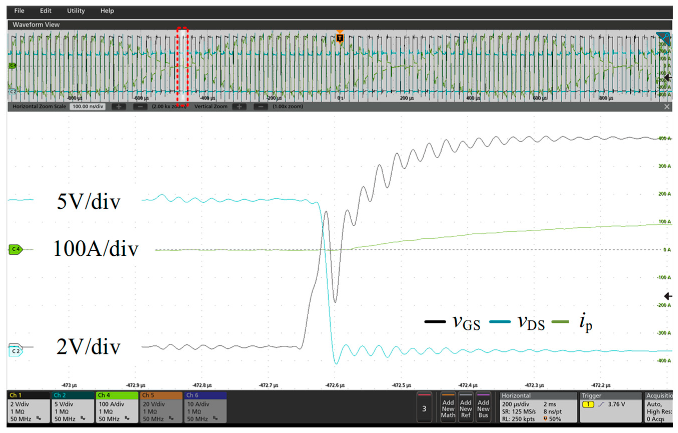
In contrast, the lagging-arm switches face a more challenging ZVS condition. During the dead-time interval of the lagging arm, the available current to commutate the output capacitances is primarily supplied by the magnetizing current of the high-frequency transformer, since the resonant current is near zero at the zero-crossing of the output current. The magnetizing current is determined by the input voltage and the magnetizing inductance and is therefore relatively independent of the load. As the load decreases, the resonant current component diminishes, and the total available commutation current approaches the magnetizing current alone. When the load is reduced below a certain threshold (approximately 25–30% of full load in the present design), the magnetizing current becomes insufficient to fully charge or discharge the MOSFET output capacitances within the fixed dead-time, causing the lagging-arm switches to lose ZVS. This phenomenon is clearly observed in Figure 24, where the lagging-arm switch voltage waveform exhibits a hard-switching turn-on transient at the zero-crossing point of the output current.
Figure 24.
The lagging bridge arm does not achieve the ZVS waveform at the point where the output voltage crosses zero.
It should be noted that the loss of ZVS in the lagging arm at light load has a limited impact on the overall system efficiency. This is because (i) the total power level at light load is inherently low, so the absolute switching loss is small; (ii) the inverter stage operates at a relatively low fundamental frequency of 750 Hz, where switching losses are already a small fraction of the total losses compared to conduction losses; and (iii) the leading-arm switches continue to operate with ZVS, preserving the majority of the high-frequency switching losses advantage. Nevertheless, for applications requiring high efficiency over a wide load range, design modifications such as increasing the magnetizing inductance or employing variable dead-time control could be considered to extend the ZVS range.
4.2. Steady-State Experiment
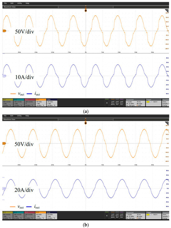
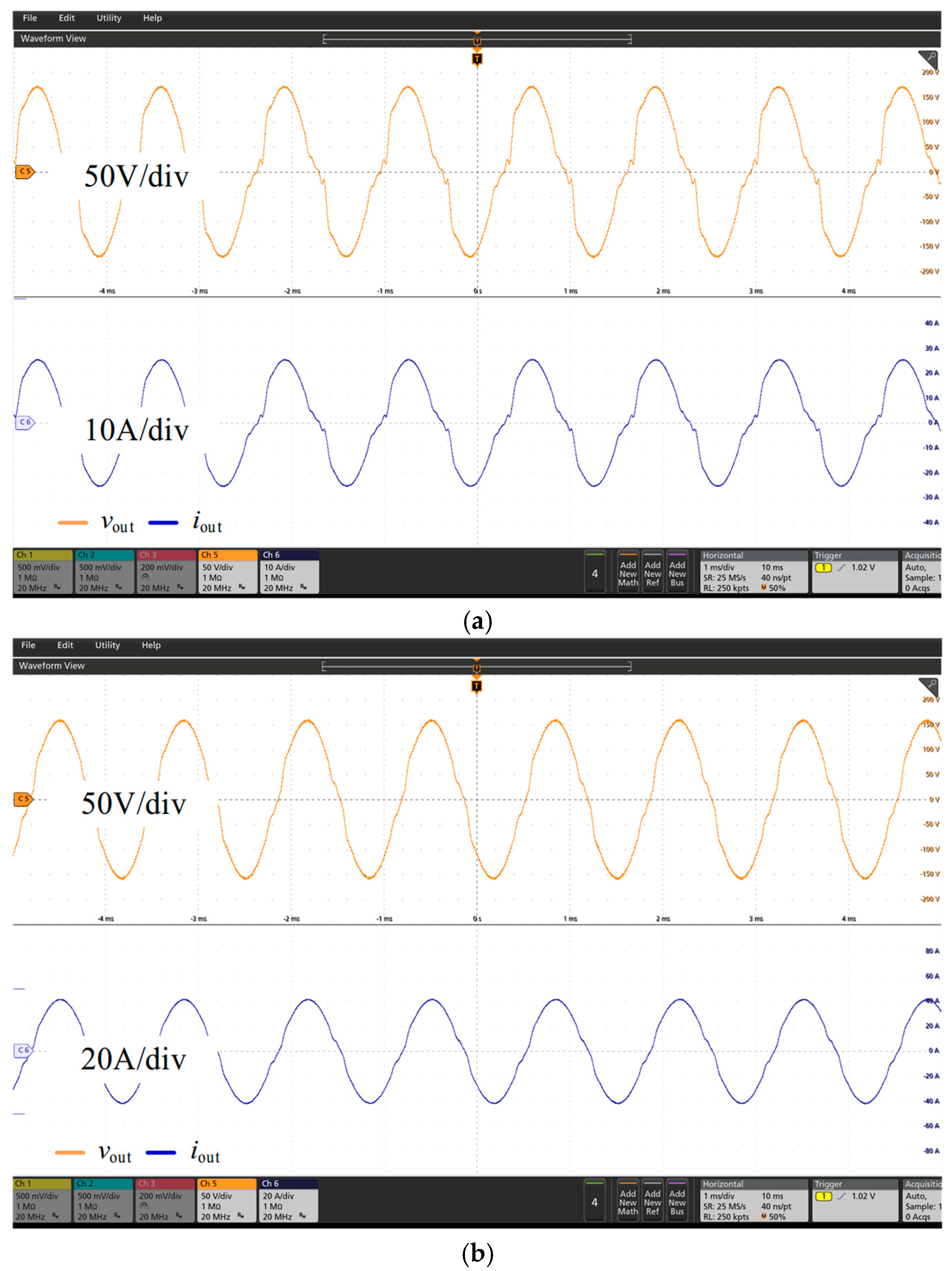
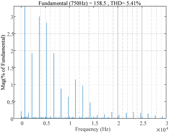
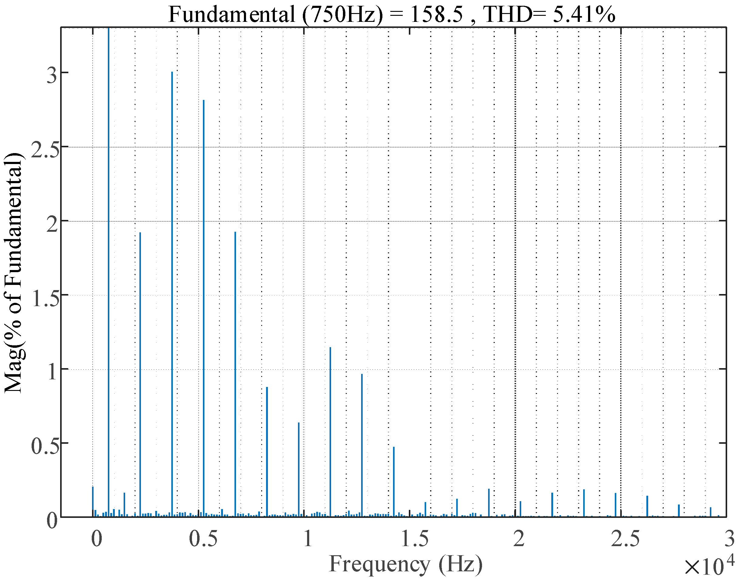
The steady-state experimental conditions were PSFB-HFL inverter with closed-loop output, input of 28 VDC, and full-load output power of 4 kW. The output waveforms of the inverter under half-load and full-load conditions are shown in Figure 25, with channel 5 representing the output voltage waveform and channel 6 representing the output current waveform. The full-load output voltage was subjected to FFT processing, and the results are shown in Figure 26. The measured output voltage THD is 5.41%. In accordance with the design specifications for more electric aircraft (MEA) starter power units (SPU) and the established practices in airborne power electronics design (e.g., Boeing B787), the total harmonic distortion (THD) constraint for the grid-side current in the aircraft SPU application scenario is set to ≤10%. This design target complies with the airborne power quality requirements specified in DO-160 and MIL-STD-704F standards.
Figure 25.
Half- and full-load output waveform diagram of PSFB-HFL inverter. (a) Po = 2 kW; (b) Po = 4 kW.
Figure 26.
Full-load output voltage Fourier analysis graph of PSFB-HFL inverter.
4.3. Dynamic Experiment
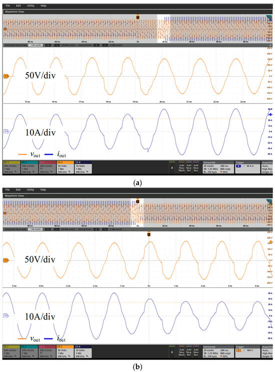
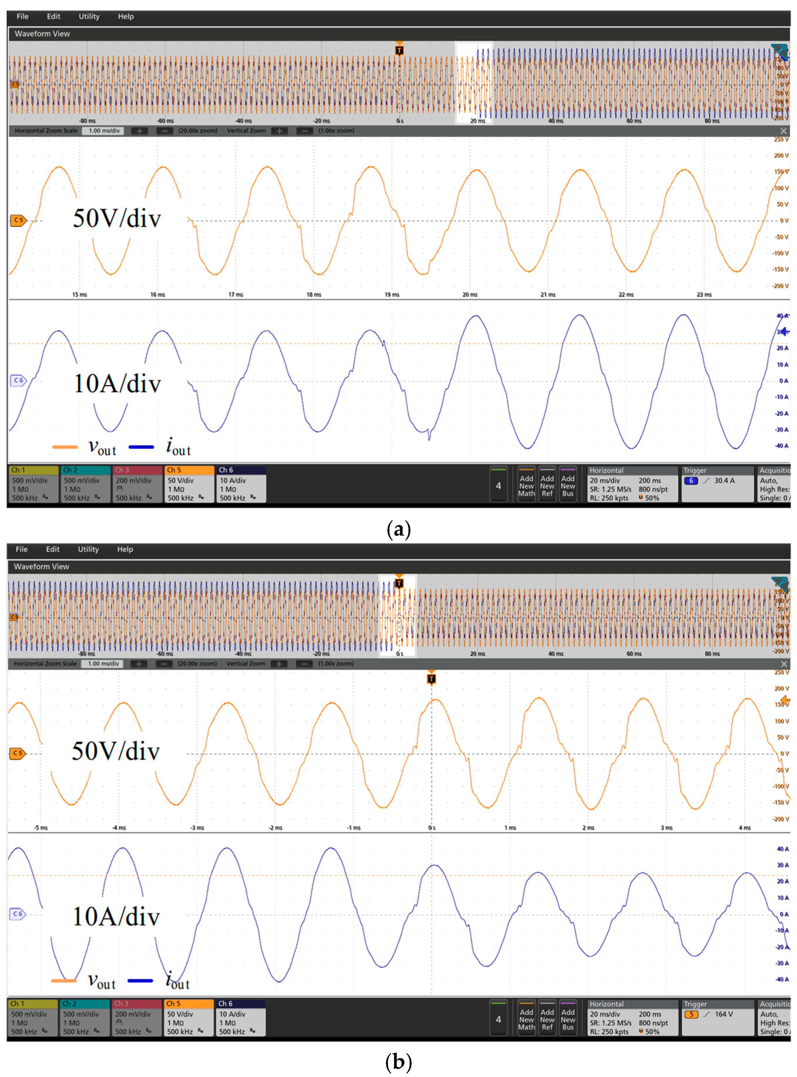
When the rated input voltage is 28 V DC, the dynamic performance of the system was tested through the experiments of half-load to full-load and full-load to half-load switching. The specific results are shown in Figure 27. Channel 5 represents the output voltage waveform, and Channel 6 represents the output current waveform. The experimental results show that the system maintains stable sinusoidal output voltage and current waveforms without any visible sub-harmonic oscillation or instability. The continuous and convergent operation across consecutive cycles validates the proposed control scheme’s large-signal stability and robust performance under heavy load conditions.
Figure 27.
Dynamic performance experiment graph of PSFB-HFL inverter. (a) Half-load to full-load switching; (b) full-load to half-load switching.
4.4. Efficiency Analysis and Loss Breakdown
The experimental results demonstrate that the front-stage PSFB DC–DC converter achieves a peak efficiency of 93.5% at full load, whereas the overall inverter system efficiency is measured at 87%. This 6.5% efficiency drop is primarily attributed to the power losses introduced by the post-stage H-bridge inverter and the output filter. A detailed breakdown of the loss distribution is provided below to account for this discrepancy.
(1) Losses in the DC–DC Stage (Efficiency: 93.5%):
The power loss in the front stage is dominated by the conduction and switching losses of the primary-side MOSFETs, as well as the conduction loss of the secondary-side rectifier diodes. Additionally, the high-frequency transformer contributes to both copper loss (due to AC resistance and proximity effect) and core loss. The RC snubber circuits, designed to suppress voltage spikes, dissipate approximately 25 W of power. It is worth noting that the gate-drive loss for the primary MOSFETs is negligible (approximately 0.92 W for six devices), accounting for less than 0.03% of the total power.
(2) Losses in the Inverter Stage (Accounting for the 6.5% Drop):
The significant efficiency drop from the DC–DC stage to the total system is mainly caused by the post-stage inverter. Although the inverter operates at a relatively low fundamental frequency of 750 Hz, resulting in minimal switching losses and negligible gate-drive consumption (approximately 0.008 W for four devices), its conduction losses are substantial. This is due to the use of high-voltage MOSFETs in the H-bridge, which typically exhibit higher on-state resistance Rds(on) compared to the low-voltage devices used in the DC–DC stage. Furthermore, during the dead-time intervals, the body diodes of the inverter MOSFETs conduct the load current, introducing additional conduction losses due to their higher forward voltage drop. Finally, the output LC filter, essential for attenuating high-frequency harmonics, incurs considerable copper loss in the filter inductor and ESR loss in the filter capacitor.
In summary, the total system loss of approximately 13% (yielding 87% efficiency) is the cumulative result of the DC–DC stage losses (6.5%) and the inverter stage losses (6.5%). The dominant loss mechanisms in the inverter stage are the conduction losses of the high-voltage switches and the output filter losses, rather than switching or drive losses.
5. Conclusions
This paper summarizes and analyzes the sub-harmonic oscillation problem existing in the implementation of peak current control for the PSFB-HFL inverter. Based on the small-signal modeling theory of Buck converters, an accurate small-signal model of the PSFB peak current inner loop is established, and a corresponding slope compensation scheme is designed to eliminate sub-harmonic oscillation. On this basis, a voltage outer-loop PI controller is developed to optimize the closed-loop dynamic performance of the DC to sinusoidal-half-wave to sinusoidal-wave conversion structure. The adopted PSFB-HFL inverter features fewer passive components, low post-stage switching frequency and low power loss, which is suitable for airborne low-voltage high-current and high step-up ratio applications and has the potential to realize combined three-phase output. Finally, a principle prototype with a 28 V DC input and a rated power of 4 kW was fabricated. The experimental results confirm that the proposed control scheme enables the PSFB-HFL inverter to achieve robust large-signal stability under varying load conditions. The system maintains high-quality sinusoidal output without sub-harmonic oscillation or distortion, even during significant load perturbations.
Author Contributions
Conceptualization, X.C.; methodology, X.C.; software, M.L.; validation, M.L.; formal analysis, X.C.; investigation, M.L.; resources, X.Z. and X.W.; data curation, X.Z.; writing—original draft preparation, M.L.; writing—review and editing, X.C. and X.W.; visualization, X.L.; supervision, X.C.; project administration, X.W.; funding acquisition, X.C. All authors have read and agreed to the published version of the manuscript.
Funding
This research was funded in part by the Guangdong Basic and Applied Basic Research Foundation, grant number 2021A1515110039 and in part by the Youth Project of the Natural Science Foundation of Shaanxi Province, grant number 2025JC-YBQN-517, and in part by the China Postdoctoral Science Foundation General Project, grant number 2022M711992, and in part by the Fundamental Research Funds for the Central Universities, grant number D5000220070.
Data Availability Statement
Data are contained within the article.
Conflicts of Interest
The authors declare no conflicts of interest.
References
- Zhu, J.; Duan, Y.; Wu, H.; Yang, F.; Chen, G.; Xing, Y. Dual DC Bus Rectifier With Embedded Power Decoupling for Airborne Pulsed Load Application. IEEE Trans. Transp. Electrif. 2026, 12, 3394–3404. [Google Scholar] [CrossRef] [Scilit]
- Ji, Y.; Giangrande, P.; Zhao, W.; Wang, H.; Zhang, P. Development of an Insulation Lifetime Model Under Varied Pressure and Voltage Conditions for More Electric Aircraft Applications. IEEE Trans. Transp. Electrif. 2026, 12, 6326–6337. [Google Scholar] [CrossRef] [Scilit]
- Imperiali, L.; Kolar, J.W.; Huber, J. Environmental Assessment of Ultralightweight DC–DC Converters for Future eVTOL Aircraft With Hybrid Power Supply. IEEE J. Emerg. Sel. Top. Ind. Electron. 2026, 7, 1390–1394. [Google Scholar] [CrossRef] [Scilit]
- Chen, X.; Shi, Y.; He, H.; Zhao, X.; Li, X.; Wu, X. Research on FSBB Converter Based on Sub-Peak Current Constant Frequency Control. Electronics 2026, 15, 2845. [Google Scholar] [CrossRef] [Scilit]
- Corcau, J.I.; Dinca, L. More electricity on modern civil aircrafts-review. In Proceedings of the 2020 24th International Conference on Circuits, Systems, Communications and Computers (CSCC), Chania, Greece, 19–22 July 2020; pp. 226–229. [Google Scholar] [CrossRef] [Scilit]
- Zharkov, M.A.; Sarakhanova, R.Y. Analysis of current state of the starting device for aircraft gas turbine engines. In Proceedings of the 2020 International Ural Conference on Electrical Power Engineering (UralCon), Chelyabinsk, Russia, 22–24 September 2020; pp. 383–388. [Google Scholar] [CrossRef] [Scilit]
- Sarlioglu, B.; Morris, C.T. More Electric Aircraft: Review, Challenges, and Opportunities for Commercial Transport Aircraft. IEEE Trans. Transp. Electrif. 2015, 1, 54–64. [Google Scholar] [CrossRef] [Scilit]
- Chen, L.; Gao, H.; Shen, F.; Zhang, Y.; Qiu, L.; Wang, L. A Novel Magnetic Integration High-Efficiency Converter with Low Ripple and High Dynamic Response for the Hybrid Power Supply Systems of All-Electric Aircraft. Aerospace 2024, 11, 965. [Google Scholar] [CrossRef] [Scilit]
- Radomsky, L.; Keilmann, R.; Ferch, D.; Mallwitz, R. Challenges and opportunities in power electronics design for all- and hybrid-electric aircraft: A qualitative review and outlook. CEAS Aeronaut. J. 2024, 15, 751–764. [Google Scholar] [CrossRef] [Scilit]
- Ridley, R. A new, continuous-time model for current-mode control. IEEE Trans. Power Electron. 1991, 6, 271–280. [Google Scholar] [CrossRef] [Scilit]
- Tiwary, A.; Rincón-Mora, G.A. Sub-Harmonic Stability and Slope Compensation Boundary in Peak/Valley DC–DC Converters. Electronics 2026, 15, 1609. [Google Scholar] [CrossRef] [Scilit]
- Liu, B.; Tang, Y.; Ge, L.; Niu, J. Feedforward Compensation for Phase-Shifted Full-Bridge DC–DC Converter Under Peak Current Mode Control. IEEE Trans. Power Electron. 2024, 39, 6840–6851. [Google Scholar] [CrossRef] [Scilit]
- Tan, B.; Liang, Z.; Chung, C.; Dong, H.; Yin, X.; Rayeem, S.K.; Zhu, J. Uncertainty-Aware Approaches Toward Managing Hydrogen-Powered Vehicles and Renewable Energy Units in Microgrid–Transportation Networks. IEEE Trans. Transp. Electrif. 2026. [Google Scholar] [CrossRef] [Scilit]

Disclaimer/Publisher’s Note: The statements, opinions and data contained in all publications are solely those of the individual author(s) and contributor(s) and not of MDPI and/or the editor(s). MDPI and/or the editor(s) disclaim responsibility for any injury to people or property resulting from any ideas, methods, instructions or products referred to in the content. |
© 2026 by the authors. Licensee MDPI, Basel, Switzerland. This article is an open access article distributed under the terms and conditions of the Creative Commons Attribution (CC BY) license.