


Abstract
This paper presents two antenna array designs, an equal-phase array and a monopulse array, implemented using dielectric 3D-printing technology. To achieve wideband operation and low back-lobe radiation, a novel magneto-electric dipole (ME-dipole) element is first proposed. This element is derived from an open-ended waveguide; the open aperture functions as a magnetic dipole, while a pair of metallic patches placed at the aperture forms an electric dipole. Through structural evolution, the element is adapted for post-processing after 3D printing. The two arrays are then developed using this element. The equal-phase array employs a three-stage cascaded T-junction feeding network, whereas the monopulse array replaces the first-stage T-junction with a Magic-T coupler. The main bodies of both arrays are printed from dielectric material, and selected surfaces are copper-electroplated to form the necessary metallic components. The proposed arrays offer simple fabrication, low weight, and good performance. Measurements show that the equal-phase and monopulse arrays achieve overlapped bandwidths of 32.8% and 35.6% and peak gains of 13.1 and 13.5 dBi, respectively. The measured null depth of the monopulse array is below −32.3 dB.
1. Introduction
3D printing is an emerging manufacturing technology that produces three-dimensional structures by depositing material layer by layer. Unlike conventional subtractive processes, 3D printing is an additive manufacturing method that offers high material utilization, suitability for complex structures, and short production cycles [1,2,3]. It has been widely applied in industrial manufacturing, aerospace, medicine, and architecture [4,5,6,7]. In recent years, 3D printing has also attracted extensive research interest and found broad applications in antenna engineering.
According to the material used to form the printed structure, 3D-printed antennas can be broadly classified as metallic [8,9,10,11,12,13,14] and dielectric types [15,16,17,18,19,20,21]. Among them, metallic antennas are commonly fabricated using direct metal laser sintering (DMLS), laser powder bed fusion (LPBF), and related processes, with aluminum alloys, copper, and stainless steel among the most widely used materials [2]. Metallic 3D printing has been successfully applied to various antenna elements, including horn antennas [8,9,10], fractal antennas [11], resonant-cavity antennas [12], and so on. At the array level, large-scale metallic 3D-printed designs have also been reported, including an 8 × 8 array with differential feeding cavities [13] and a 16×16 horn antenna array [14]. Metallic 3D printing can achieve a fabrication quality comparable to that obtained using conventional computer numerical control (CNC) machining, as employed in [22], and antennas fabricated using this technology generally exhibit good performance. However, the relatively high density of metals increases antenna weight and limits practical deployment. This drawback is particularly significant for waveguide-based antenna arrays.
Dielectric 3D-printed antennas are commonly fabricated using fused deposition modeling (FDM), stereolithography apparatus (SLA), and PolyJet processes. Typical materials include polylactic acid (PLA), polyethylene terephthalate glycol (PETG), acrylonitrile butadiene styrene (ABS), and resins. Numerous dielectric 3D-printed antenna designs have been reported, including dielectric resonator antennas (DRA) [15,16,17] and lens antennas [18,19,20,21]. However, most dielectric 3D-printed antennas are individual elements, and comparatively few array designs have been proposed; consequently, their achievable gain is often limited. Although lens antennas can provide high gain, they generally suffer from excessive profile height or large volume, as exemplified by Luneburg lenses. In addition to fully metallic and fully dielectric 3D-printed antennas, several hybrid metal-dielectric 3D-printed arrays have recently been reported [23,24]. However, these designs often require more complex fabrication processes, and in some cases, the entire array must be divided into multiple components and then assembled.
In this work, two antenna arrays are proposed using dielectric 3D-printing technology. Both employ a novel magneto-electric dipole (ME-dipole) as the radiating element; one is an equal-phase array, and the other is a monopulse array. The main bodies of both arrays are fabricated by dielectric 3D printing, with the radiating elements and feeding networks formed as integrated structures. To realize the required conductive features, including the metallic patches, reflectors, and waveguide walls, selected surfaces of the printed bodies are metallized by electroplating. In this work, the ME-dipole is selected because of its wide bandwidth, high front-to-back ratio (FBR), and stable radiation characteristics [25,26,27,28]. Starting from the initial design, the structure of the ME-dipole element is progressively evolved to improve manufacturability without compromising antenna performance.
The novelty and contributions of this work can be summarized as follows. First, a novel ME-dipole element, which is compatible with dielectric 3D-printing and electroplating processes while offering a wide bandwidth, a high FBR, and stable operating performance, is proposed. Second, most previously reported dielectric 3D-printed antennas have focused on individual antenna elements, whereas this work represents one of the relatively few studies on dielectric 3D-printed antenna arrays. Compared with previously reported metal 3D-printed and hybrid metal–dielectric 3D-printed antenna arrays, the proposed design offers the advantages of lower weight, a more compact size, and a simpler fabrication process. By developing and experimentally validating both equal-phase and monopulse array configurations, the feasibility and advantages of dielectric 3D-printing technology for the realization of antenna arrays are demonstrated. In this paper, all the simulations were performed by using the full wave simulation software Ansys HFSS version 2020.
2. Design of the ME-Dipole Element
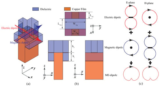
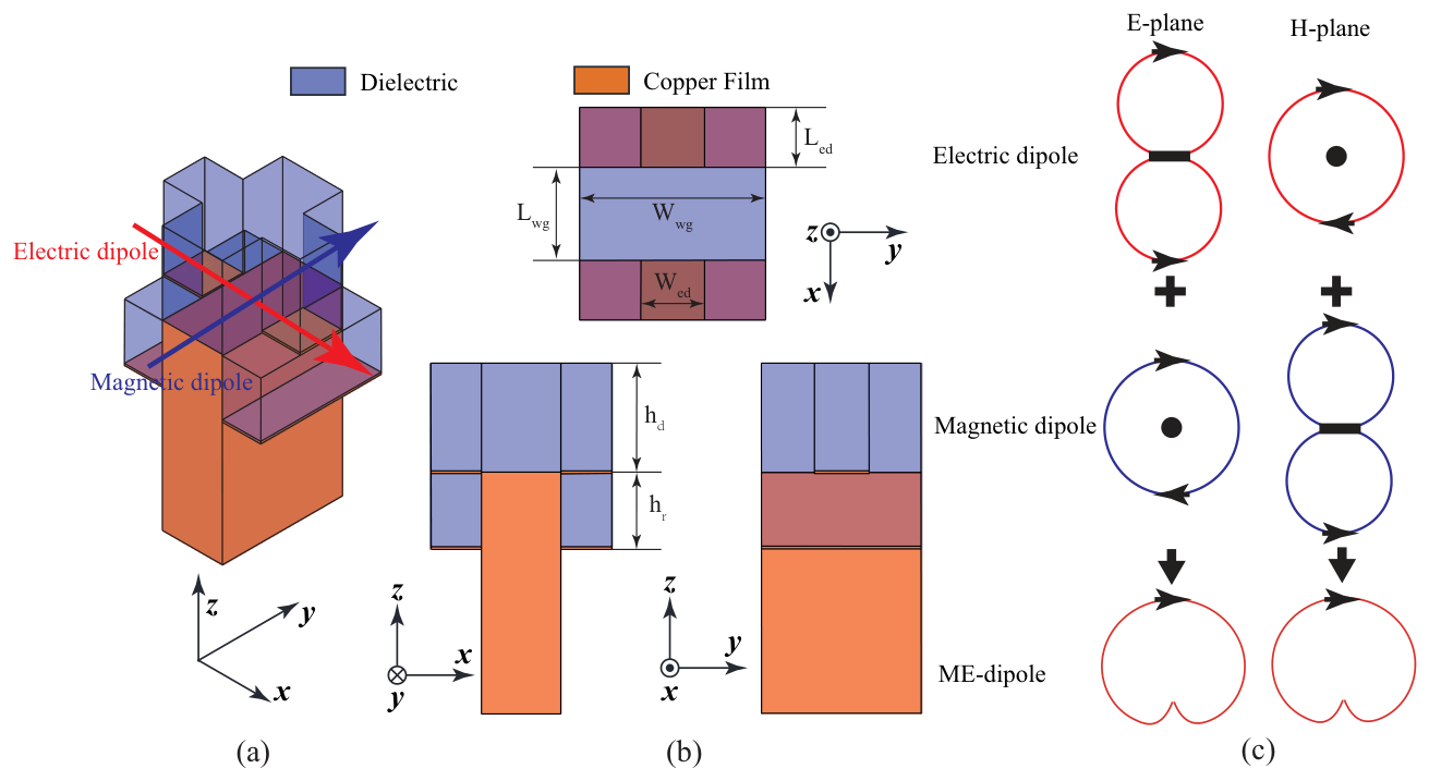
The configuration of the proposed ME-dipole element is illustrated in Figure 1. It consists of a rectangular waveguide, a cross-shaped dielectric block, and two rectangular dielectric blocks. The rectangular waveguide is fully filled with a dielectric material whose relative permittivity and loss tangent are = 2.9 and = 0.01 [29,30], respectively, and its four metallic sidewalls are formed by plating copper films onto the dielectric surfaces. The cross-shaped dielectric block is positioned above the waveguide aperture and extends along the z-axis from the aperture. Copper films are plated onto the two lower surfaces of its arms extending along the x-direction, forming two metallic patches that serve as the electric dipole. The two rectangular dielectric blocks are located on either side of the broad walls of the waveguide, and their lower surfaces are copper-plated to form a reflector structure. The locations of the electric and magnetic dipoles are indicated in Figure 1a. Figure 1c illustrates the operating principle of the ME-dipole element. For the electric dipole, the radiation patterns in the E-plane and H-plane are figure-eight-shaped and O-shaped, respectively. In contrast, the corresponding patterns of the magnetic dipole are O-shaped and figure-eight-shaped, respectively. When the two dipoles are arranged orthogonally, their forward-radiated fields add constructively because they are in phase, whereas their backward-radiated fields cancel because they are out of phase. Consequently, the ME-dipole produces a cardioid radiation pattern with a low back-lobe, thereby achieving high-gain directional radiation.
Figure 1.
Configuration and operating principle of the proposed ME-dipole antenna element. (a) Full view and (b) side views of the configuration. (c) Operating principle.
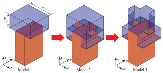
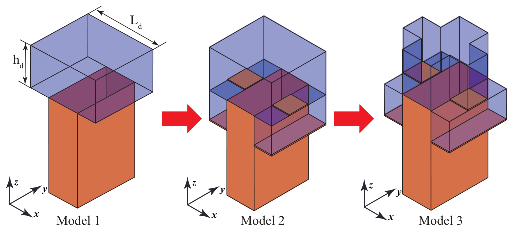
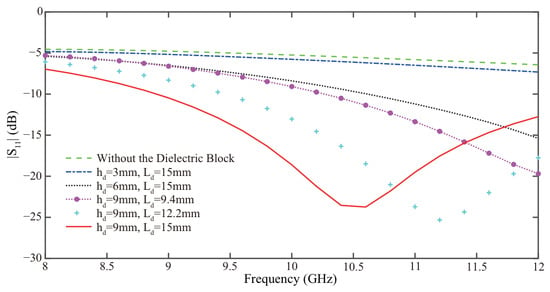
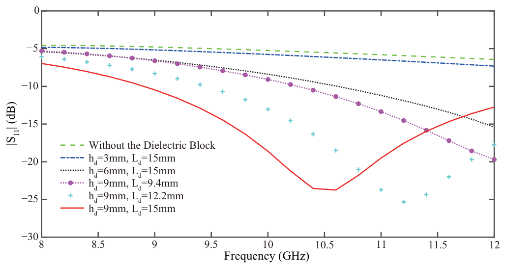
The design evolution of the proposed ME-dipole element is presented in Figure 2. The element operates in a manner similar to a traveling-wave antenna and therefore inherently exhibits wideband characteristics. However, in the absence of the dielectric block, the open waveguide aperture forms an abrupt air–dielectric interface that causes substantial wave reflection. Consequently, the reflection coefficient of the element is only approximately −5 dB, as shown in Figure 3. To improve the impedance matching, a rectangular dielectric block with dimensions of is introduced at the waveguide aperture, as shown in Model 1. The dielectric block serves as a transition between the dielectric-filled waveguide and free space, allowing the wave to propagate smoothly from the waveguide into the surrounding air. As indicated by the results in Figure 3, the impedance matching of the element gradually improves as the dimensions of the dielectric block increase. When the height and width approach 0.5 and 1, respectively, good impedance matching can be achieved. Here, is the guided wavelength at the center frequency of 10 GHz, with = / = 17.6 mm, and is the free-space wavelength at 10 GHz.
Figure 2.
Design evolution of the proposed ME-dipole antenna element.
Figure 3.
Effect of the rectangular dielectric cube on impedance matching.
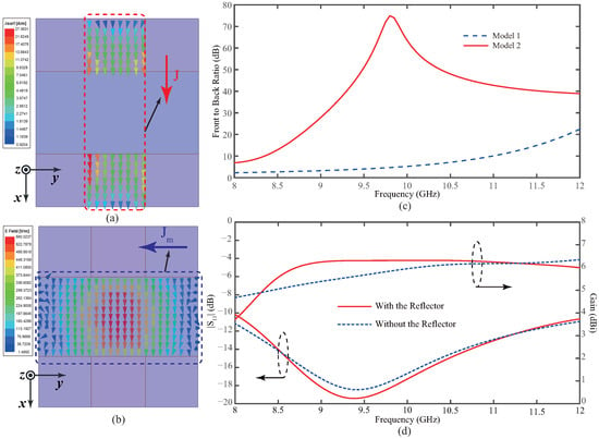
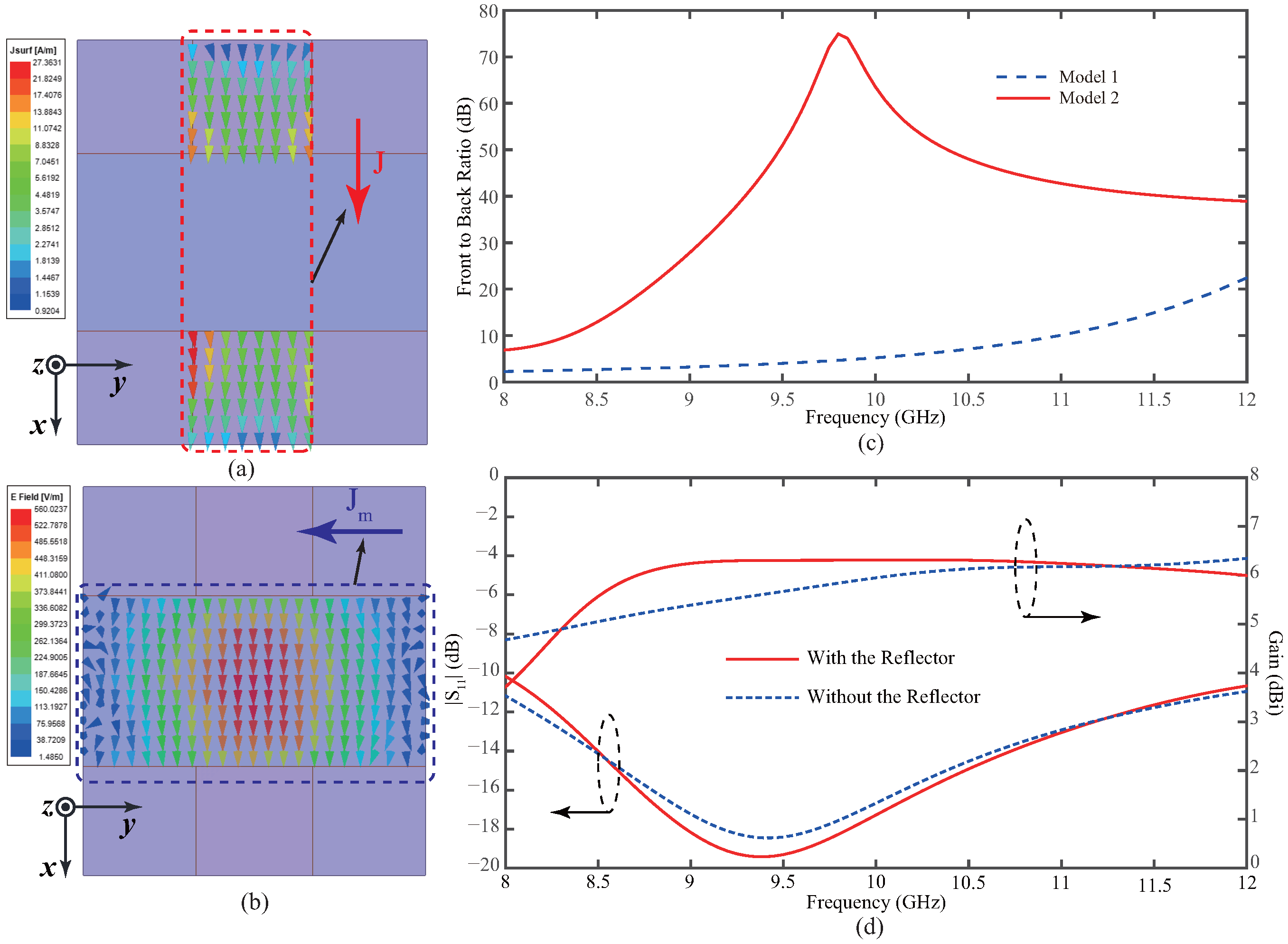
Based on Model 1, an electric dipole and reflector structures are then introduced to form Model 2, as illustrated in Figure 2. Figure 4a,b show the simulated surface-current distribution on the metallic patches and the electric-field distribution at the waveguide aperture, respectively. The results indicate that the two metallic patches operate as an electric dipole, whereas the waveguide aperture functions as a magnetic dipole. The electric and magnetic dipoles are arranged orthogonally in the -plane. Consequently, their radiated fields interfere constructively in the direction and destructively in the direction. The proposed element therefore achieves unidirectional radiation toward the direction with a high FBR. Figure 4c compares the FBRs of Models 1 and 2. After the electric dipole is introduced, the FBR is significantly improved across the entire operating band, reaching a maximum of approximately 74 dB. These results confirm that the proposed element operates according to the ME-dipole principle and that the electric and magnetic dipoles exhibit effective complementary radiation characteristics. In addition, as shown in Figure 4d, the reflectors introduced in Model 2 can improve the gain by approximately 1 dB in the lower-frequency range of 8.5–10.5 GHz while having a negligible effect on the reflection coefficient.
Figure 4.
Simulated (a) surface currents on the metallic patches and (b) electric fields at the waveguide aperture. (c) Comparison on FBRs between Model 1 and Model 2. (d) Comparisons on and gain of Model 2 with and without the reflectors.
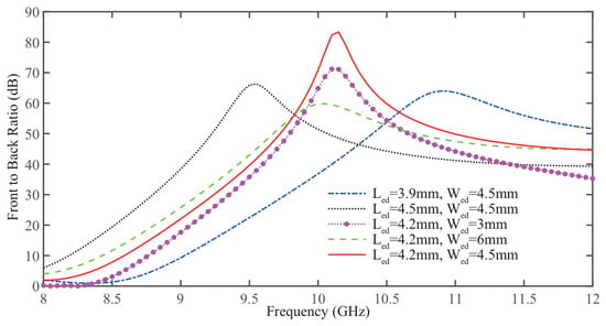
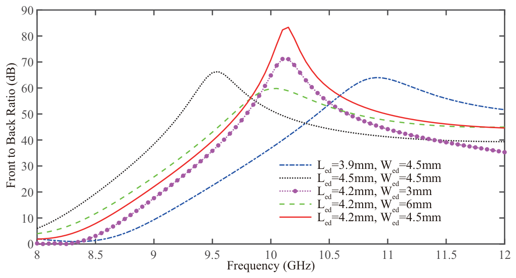
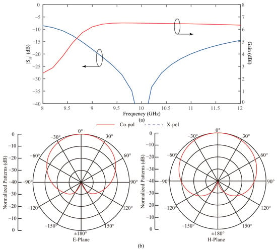
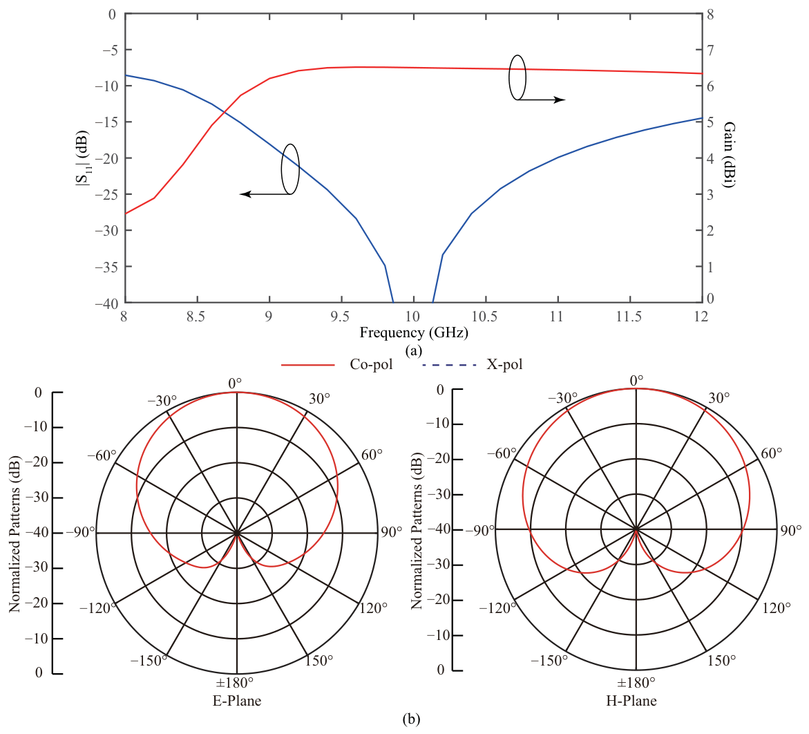
Although Model 2 already exhibits a satisfactory ME-dipole response, its two metallic patches are embedded within the dielectric block, making the subsequent metallization process difficult. To address this fabrication challenge, the rectangular dielectric block above Model 2 is modified into a cross-shaped structure, resulting in Model 3. During fabrication, the cross-shaped dielectric block and rectangular waveguide can be 3D-printed as a single piece, after which only the waveguide walls and the lower surfaces of the cross-shaped block need to be metal-plated. The two dielectric blocks supporting the reflectors can be printed and metal-plated separately before all the components are assembled. It is worth noting that the strongest electromagnetic fields within the dielectric block are concentrated near its central region. Therefore, changing the block from a rectangular to a cross-shaped configuration does not substantially affect the element performance. Minor variations in the radiation characteristics can be compensated by adjusting the dimensions of the metallic patches while monitoring the FBR. The effects of different metallic-patch dimensions on the FBR are presented in Figure 5. As shown in Figure 5, the length of the electric dipole affects the operating frequency of the antenna. Accordingly, the frequency at which the maximum FBR occurs shifts as varies. Increasing shifts the FBR peak toward a lower frequency. In contrast, when is fixed, varying the metallic-patch width primarily affects the maximum FBR value, while the corresponding peak frequency remains nearly unchanged. This observation indicates that influences the radiation strength of the electric dipole. When = 4.2 mm and = 4.5 mm, the backward radiation from the electric and magnetic dipoles undergoes the greatest degree of cancellation, resulting in a peak FBR of approximately 84 dB. The optimized reflection coefficient and radiation characteristics of the proposed element are shown in Figure 6. The proposed element achieves an impedance bandwidth of more than 40%, covering 8–12 GHz, with a peak gain of approximately 6.5 dBi and stable radiation patterns across the operating band. The geometric parameters of the optimized element are listed in Table 1. The design procedure of the proposed element can be summarized as follows:
Figure 5.
Effect of the metallic patches on FBR.
Figure 6.
Simulated element performance. (a) and gain. (b) Radiation patterns at the center frequency.
Table 1.
Parameters of the Antenna Element. (Unit: ).
(1) Determine the dimensions of the dielectric-filled waveguide. The dielectric-filled waveguide operates in the mode; therefore, its width is generally greater than 0.5. Its thickness can be selected with reference to a standard rectangular waveguide and is typically approximately half its width. The dimensions and are optimized by examining the cutoff frequency to ensure that the desired operating frequency is above the cutoff frequency.
(2) Determine the dimensions of the dielectric block. The design begins with a rectangular dielectric block. Its height and width are gradually increased until satisfactory impedance matching is achieved. According to the results of this study, suitable values of and are approximately 0.5 and 1, respectively.
(3) Modify the dielectric block into a cross-shaped structure. Starting from the rectangular dielectric block, its four corners are removed to form a cross-shaped structure.
(4) Determine the dimensions of the metallic patches and reflectors. The initial length of each metallic patch is approximately 0.25. The patch length and width are then optimized to maximize the FBR while ensuring that the FBR peak occurs at the center frequency. The spacing between the metallic patches and the reflector is initially set to approximately 0.25 and can subsequently be fine-tuned to achieve the optimal gain performance.
3. Design of the Equal-Phase Array
3.1. Feeding Network
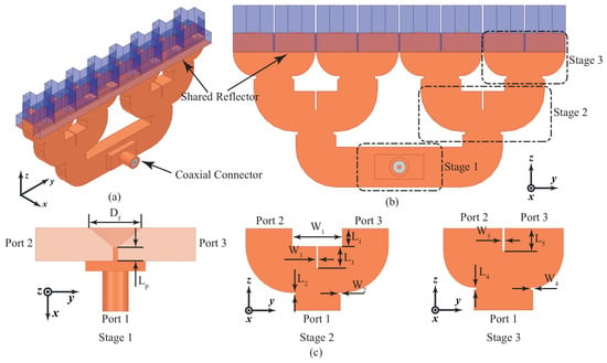
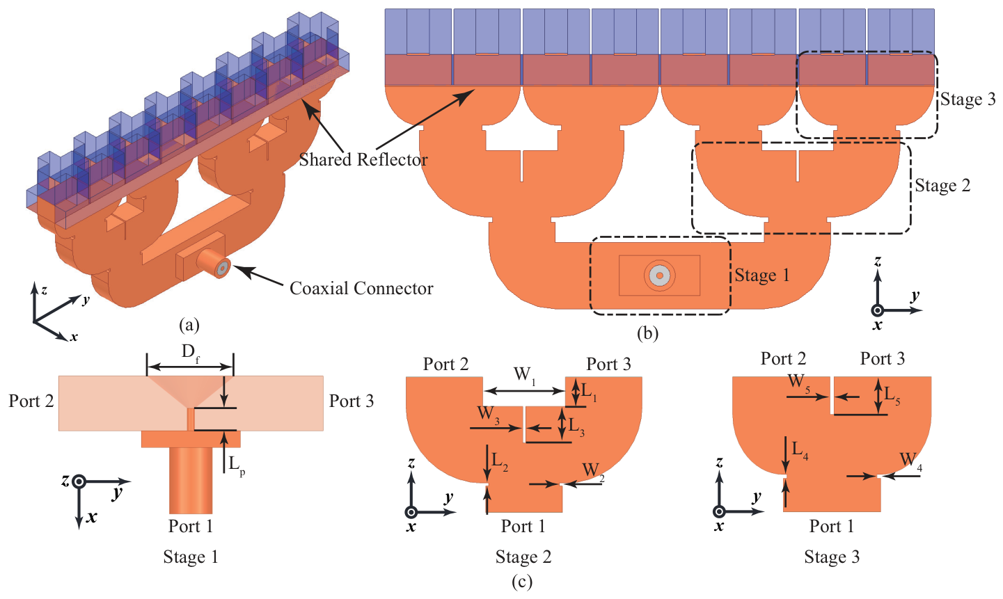
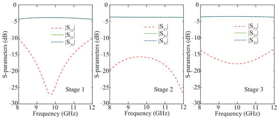
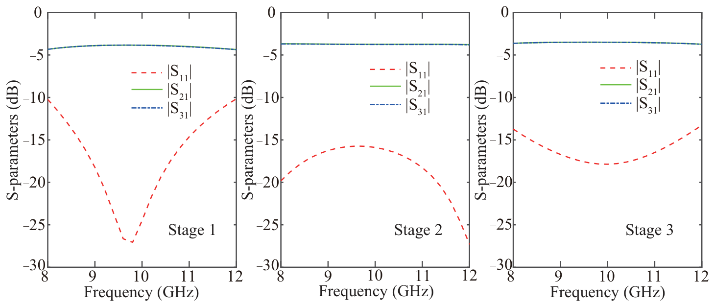
Following the element design, an equal-phase array is developed to produce endfire radiation, similar to the array reported in [31]. The configuration of the proposed array is illustrated in Figure 7. It is a one-dimensional array with an interelement spacing of . The feeding network consists of three cascaded stages of H-plane T-junction power dividers. The first-stage divider is excited through a coaxial connector whose inner conductor extends into the waveguide, while impedance matching is achieved using a conical recess. The second- and third-stage dividers employ conventional H-plane T-junctions. To suppress reflections, the waveguide bends are designed with rounded corners. Furthermore, to simplify fabrication, the reflector structures located on the same side of the array are integrated into a single continuous structure. The simulated performance of the three-stage feeding network is presented in Figure 8. All three power dividers achieve equal-power division and reflection coefficients below −10 dB over the frequency range of 8–12 GHz. Their overlapping dB impedance bandwidth extends from 8.6 to 11.3 GHz. The insertion losses of the three power dividers are approximately 0.8 dB. The geometric parameters of the feeding network of the equal-phase array are listed in Table 2.
Figure 7.
Configuration of the proposed equal-phase antenna array. (a) Full view. (b) Side view. (c) Stage 1 to Stage 3 power dividers.
Figure 8.
Simulated S-parameters of Stage 1 to Stage 3 power dividers.
Table 2.
Parameters of the Feeding Network of the Equal-Phase Antenna Array. (Unit: ).
3.2. Fabrication and Antenna Performance
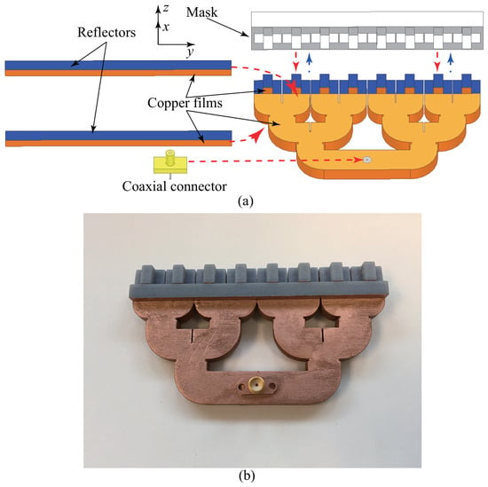
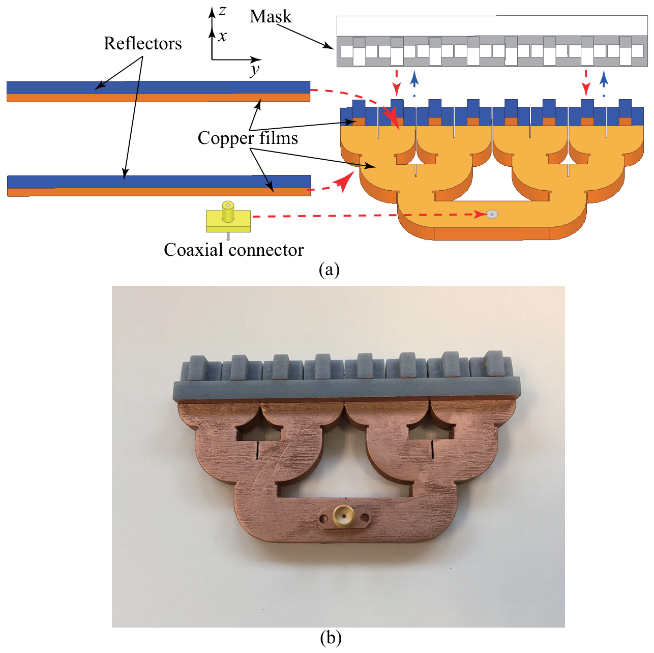
To validate the proposed design concept, a prototype of the equal-phase array was fabricated and measured. A schematic illustration of the fabrication process and a photograph of the fabricated prototype are shown in Figure 9. The prototype was fabricated from VeroBlue resin material using a Stratasys Objet30 high-precision 3D printer. During fabrication, the two reflector-supporting dielectric blocks and the main array body were printed separately, metallized individually, and subsequently assembled using cyanoacrylate adhesive. Similar to the metallization processes reported in the existing literature [32,33], the metallization process in this work consisted of three steps. The first step was masking, in which masks complementary to the array geometry were fabricated using the same 3D-printing technique to cover the regions that did not require metallization. The second step was sputtering, which deposited an initial conductive seed layer to facilitate the subsequent electroplating process. Because the heat generated during sputtering could deform the dielectric material, each sputtering cycle was limited to less than 2 min, with the maximum temperature maintained below 50 °C. After sputtering, the metallic layer on the array surface was approximately 60 nm thick. The third step was electroplating, which lasted approximately 90 min and increased the metallic-layer thickness to approximately 9 μm. To protect the feeding port during metallization, the coaxial connector was installed beforehand and secured using cyanoacrylate adhesive.
Figure 9.
(a) Illustration of the fabrication process. (b) Photograph of the fabricated prototype of the proposed equal-phase antenna array.
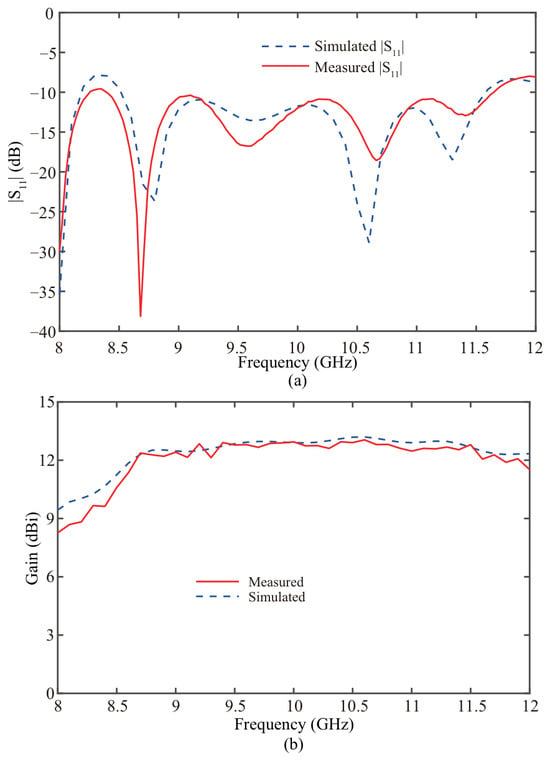
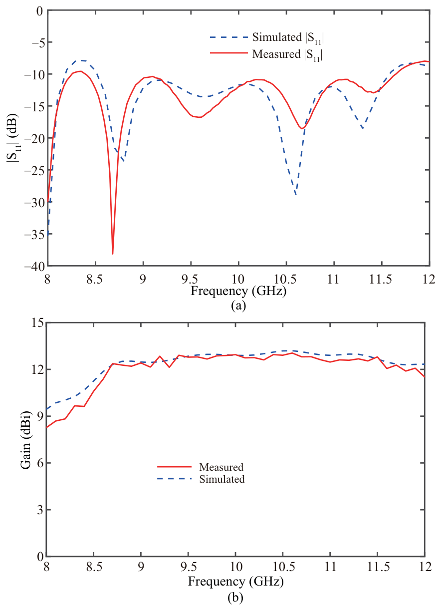
Figure 10a presents the measured and simulated reflection coefficients. The measured remains below −10 dB throughout the frequency range of 8.4 to 11.7 GHz, indicating good impedance matching. Although slight discrepancies can be observed, the measured and simulated results exhibit similar overall trends. Figure 10b shows the antenna gain as a function of frequency. The measured peak gain is 13.1 dBi at 10.5 GHz. Within 8.4 to 12 GHz, the measured gain remains variation within 3 dB. The measured results agree well with the simulations, demonstrating stable high-gain performance. The overlapped bandwidth is 32.8% from 8.4 to 11.7 GHz.
Figure 10.
Measured and simulated (a) and (b) gain of the proposed equal-phase antenna array.
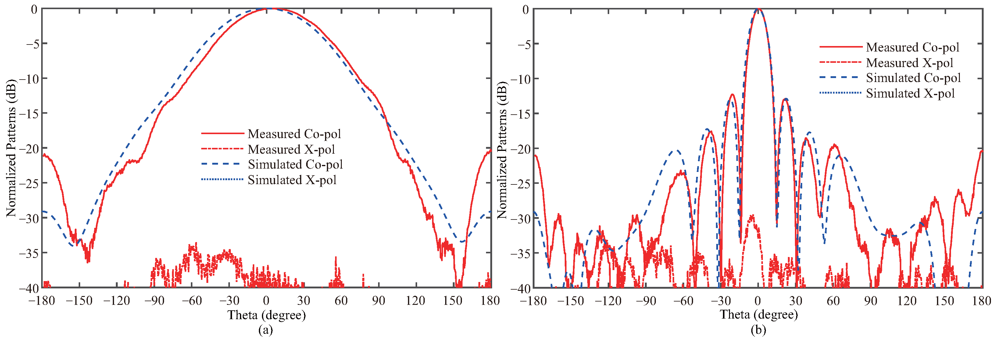
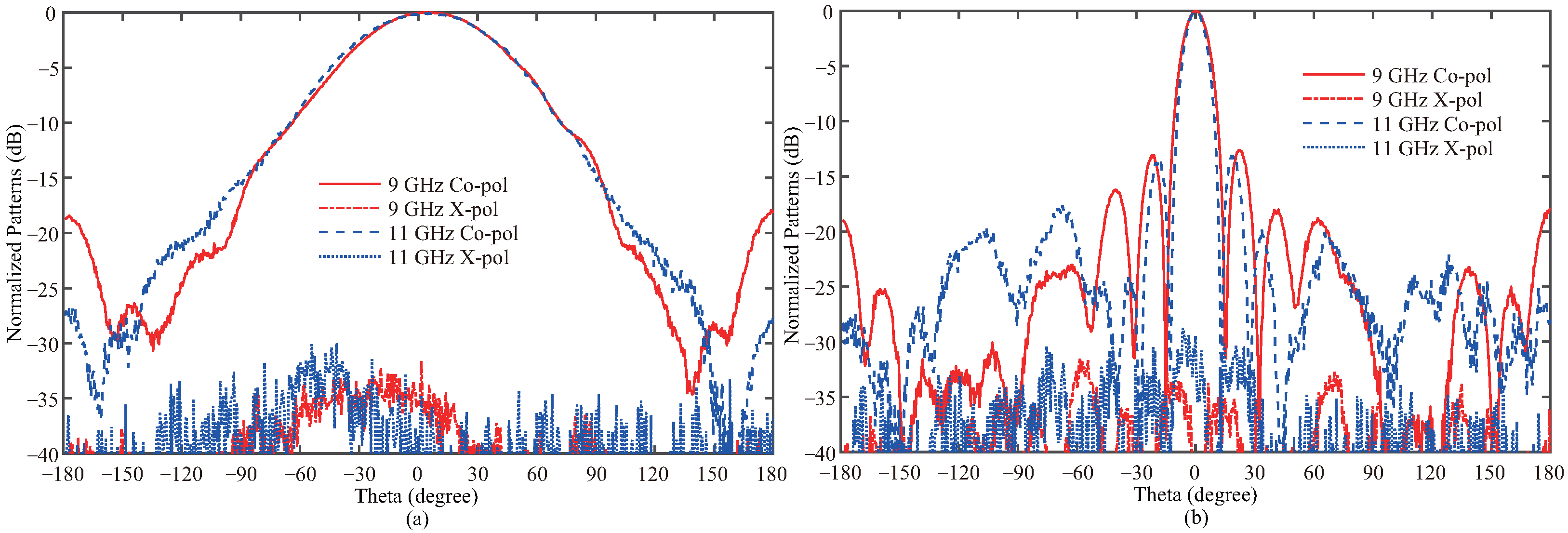
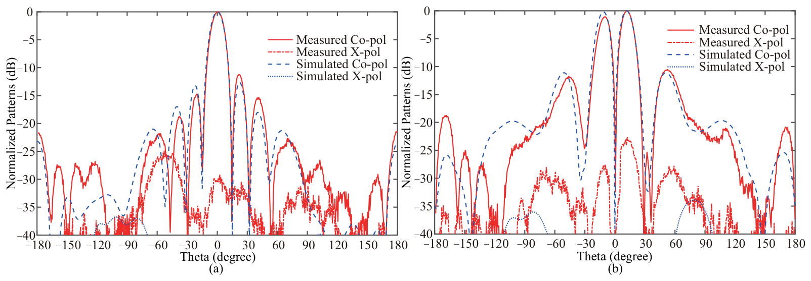
Figure 11 compares the simulated and measured normalized E- and H-plane radiation patterns at 10 GHz. Good agreement is obtained within the main-beam region in both principal planes. The measured 3 dB beamwidths are approximately in the E-plane and in the H-plane, respectively. At the broadside direction (), the measured cross-polarization levels are below dB. Figure 12 presents the measured E- and H-plane radiation patterns at 9 and 11 GHz. The measured E-plane 3 dB beamwidths are approximately and at 9 and 11 GHz, respectively, while the corresponding H-plane beamwidths are approximately . Moreover, low cross-polarization levels are maintained throughout the operating band.
Figure 11.
Measured and simulated (a) E- and (b) H-plane radiation patterns of the proposed equal-phase antenna array at 10 GHz.
Figure 12.
Measured (a) E- and (b) H-plane radiation patterns of the proposed equal-phase antenna array at 9 GHz and 11 GHz.
4. Design of the Monopulse Array
4.1. Magic-T Junction
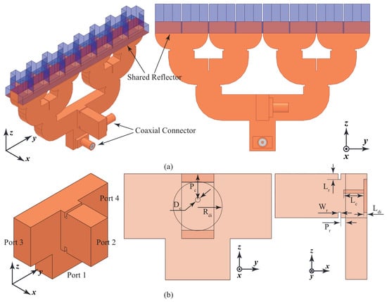
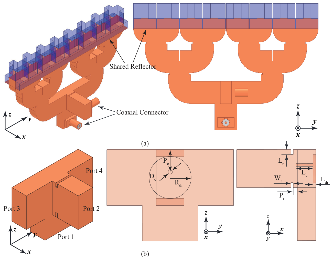
The configuration of the proposed monopulse array is presented in Figure 13. The array employs the same radiating elements as the equal-phase array, and its second- and third-stage power dividers are also identical to those used in the equal-phase array. The main difference is that the first-stage power divider is replaced by a magic-T coupler, as shown in Figure 13b. When this coupler is excited through Port 1, Ports 3 and 4 produce equal-amplitude and in-phase signals. By contrast, when it is excited through Port 2, Ports 3 and 4 produce equal-amplitude signals with a phase difference. For the monopulse array, excitation through Port 1 drives all eight radiating elements with equal amplitudes and phases. The resulting radiation characteristics are therefore identical to those of the equal-phase array, producing the sum pattern. When Port 2 is excited, the two halves of the eight-element array are driven with equal amplitudes but opposite phases, thereby producing the difference pattern.
Figure 13.
Configuration of the proposed monopulse antenna array. (a) Full and side views. (b) Magic-T coupler.
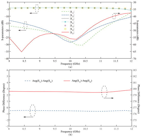
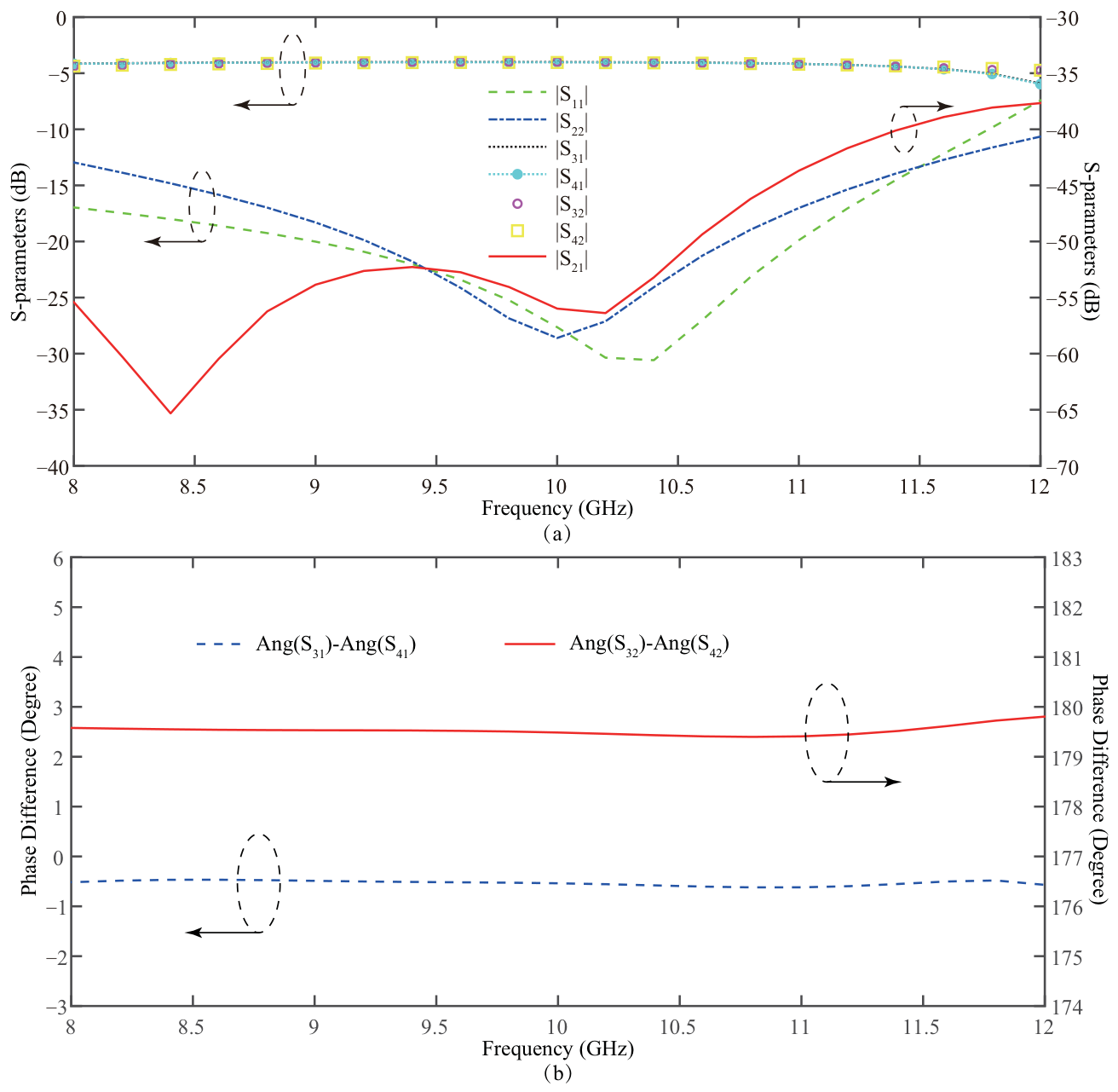
Impedance matching is a key design challenge for the magic-T coupler. To address this issue, two rectangular recesses are introduced into the waveguide section at Port 2. In addition, a circular recess with a radius of and a metallic post with a diameter of are incorporated into the rear surface of the magic-T. The metallic post is offset from the center of the circular recess, and its position is defined by the distance from the edge of the structure. During fabrication, the relatively large rectangular and circular recesses can be directly metallized through sputtering and electroplating. However, because the metallic post is only 1 mm in diameter and extends to a depth of 6.2 mm, it is difficult to deposit metal uniformly onto this narrow and deep feature through sputtering. Therefore, the post is realized by inserting a metallic pin of the same diameter. The simulated S-parameters of the proposed magic-T coupler are presented in Figure 14. Both Ports 1 and 2 achieve reflection coefficients below dB over the frequency range of 8–12 GHz. Regardless of whether Port 1 or Port 2 is excited, the input power is equally divided between Ports 3 and 4. Moreover, the isolation between Ports 1 and 2 remains better than 37.5 dB throughout the operating band. In terms of phase response, the phase difference between the two output ports is approximately under Port 1 excitation and approximately under Port 2 excitation. The geometric parameters of the proposed Magic-T coupler are listed in Table 3.
Figure 14.
Simulated S-parameters of the proposed Magic-T coupler. (a) Magnitudes. (b) Phases.
Table 3.
Parameters of the Magic-T Junction. (Unit: ).
4.2. Antenna Performance
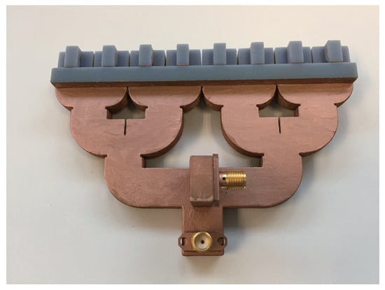
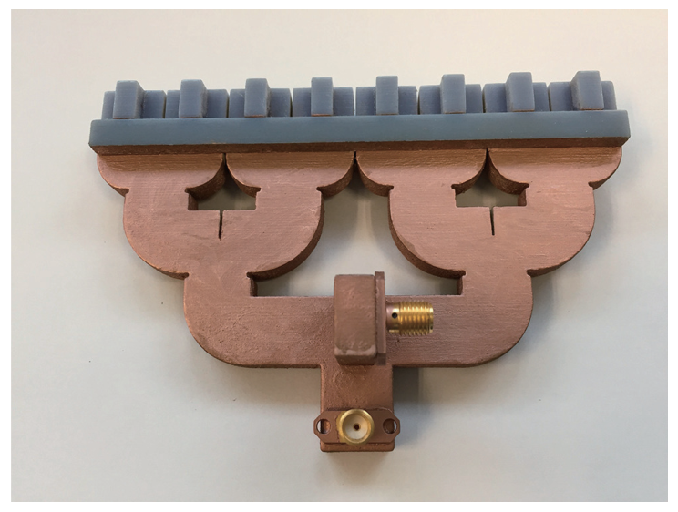
A prototype of the proposed monopulse array was also fabricated and measured. The fabrication method and procedure were identical to those employed for the equal-phase array. A photograph of the fabricated prototype is shown in Figure 15.
Figure 15.
Photograph of the fabricated prototype of the proposed monopulse antenna array.
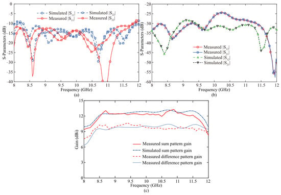
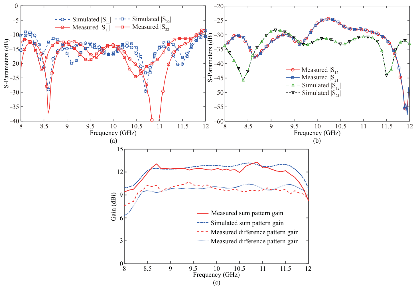
The measured and simulated S-parameters and gain of the proposed monopulse array are presented in Figure 16. As shown in Figure 16a, the measured reflection coefficients of both the sum (Port 1) and difference (Port 2) ports are below dB from 8 to 11.8 GHz, corresponding to a fractional impedance bandwidth of 38.4%. The simulated and measured reflection coefficients exhibit consistent overall trends, although some differences are observed. These discrepancies are mainly attributed to fabrication and assembly tolerances.
Figure 16.
Measured and simulated S-parameters and gain of the proposed monopulse antenna array. (a) . (b) and . (c) Gain.
Figure 16b shows the measured and simulated transmission coefficients. The parameters and are nearly identical, demonstrating the reciprocity of the feeding network. The simulated and values remain below approximately −27 dB, while the measured values remain below approximately −23 dB. The discrepancy between the simulated and measured results is mainly attributed to fabrication tolerances. Nevertheless, both the simulated and measured results demonstrate the high port isolation of better than approximately 23 dB across 8–12 GHz.
As shown in Figure 16c, the measured peak sum-channel gain is approximately 13.5 dBi and occurs near 10.8 GHz. The measured 3 dB gain bandwidth extends from approximately 8.3 to 11.9 GHz, corresponding to a fractional bandwidth of approximately 35.6%. The measured difference-channel gain is about 2.5–3 dB lower than the sum-channel gain, as expected because the differential excitation produces a broadside null instead of coherent broadside radiation. The measured and simulated gain curves show good overall agreement, with differences generally within approximately 0.5 dB for the sum channel and approximately 1 dB for the difference channel over most of the operating band.
Figure 17 compares the simulated and measured H-plane sum and difference patterns at 10 GHz. For the sum channel, the measured 3 dB beamwidth is approximately . The measured and simulated co-polarized patterns agree well within the main-beam region. The measured cross-polarization level of the sum pattern remains below approximately dB over the entire angular range and is approximately dB at . For the difference channel, the measured broadside null is dB. The measured difference-pattern cross-polarization remains below approximately dB over the entire angular range and is lower than dB at broadside. Good agreement between the simulated and measured co-polarized difference patterns is obtained.
Figure 17.
Measured and simulated (a) sum and (b) difference radiation patterns of the proposed monopulse antenna array at 10 GHz.
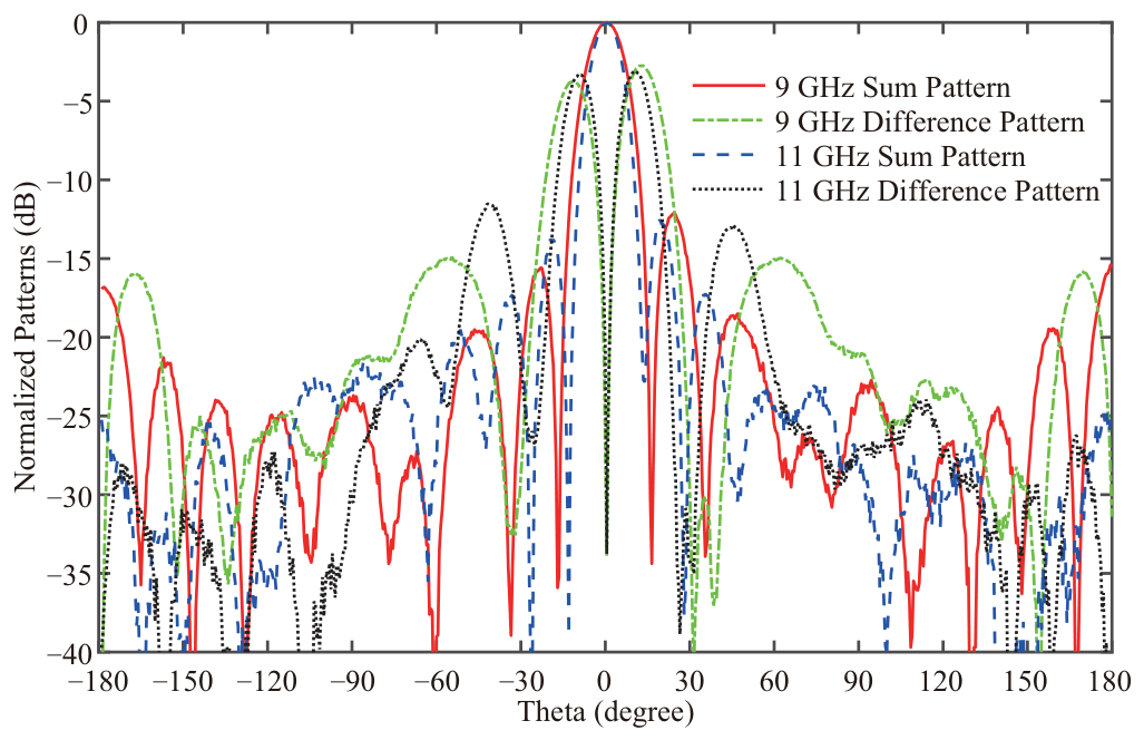
Figure 18 presents the measured H-plane sum and difference patterns at 9 and 11 GHz. For the sum beams, the measured 3 dB beamwidths are at 9 GHz and at 11 GHz. For the difference beams, the measured null depths are dB at 9 GHz and dB at 11 GHz. More generally, the measured broadside null remains below approximately dB over the operating band.
Figure 18.
Measured sum and difference radiation patterns of the proposed monopulse antenna array at 9 GHz and 11 GHz.
Table 4 compares the proposed designs with previously reported 3D-printed antenna arrays. Compared with both fully metallic 3D-printed arrays [13,14] and hybrid metal–dielectric 3D-printed arrays [23,24], the proposed antenna element has a relatively compact footprint. This compactness is enabled by its dielectric-filled waveguide configuration, which substantially reduces the required waveguide dimensions. Compared with fully metallic 3D-printed arrays, the proposed design offers the advantage of lower weight, while its fabrication process is simpler than that of hybrid 3D-printed arrays. Moreover, the proposed designs exhibits a notably wider operating bandwidth than the other reported 3D-printed arrays. Since the specific aperture efficiency values were not explicitly reported in [13,14,23], the estimated values based on the data provided in those studies are presented. In the present work, the aperture efficiencies of the equal-phase array and the monopulse array are 79.2% and 82.1%, respectively.
Table 4.
Comparison Between Reported and Proposed 3D-Printed Antenna Arrays.
5. Conclusions
Based on advanced dielectric 3D-printing technology, this paper presented a novel waveguide-based ME dipole antenna element and investigated its operating principle through theoretical and full-wave analyses. Based on the proposed element, two antenna arrays, an equal-phase array and a monopulse array, were subsequently developed. Theoretical analyses, full-wave simulations, and experimental measurements demonstrated that both arrays offer wide operating bandwidths, lightweight construction, and ease of fabrication. The proposed designs are therefore well suited to communication platforms requiring these characteristics, including unmanned aerial vehicle (UAV) communication and direction-finding systems. These results further demonstrate the feasibility and advantages of dielectric 3D printing for antenna array implementation.
Author Contributions
Conceptualization, L.L. and Z.L.M.; methodology, L.L.; software, J.M.; validation, L.L., J.M. and Z.L.M.; formal analysis, L.L.; investigation, J.M.; resources, J.M.; data curation, L.L.; writing—original draft preparation, L.L.; writing—review and editing, J.M.; visualization, L.L.; supervision, Z.L.M.; project administration, Z.L.M.; funding acquisition, Z.L.M. All authors have read and agreed to the published version of the manuscript.
Funding
This work was supported in part by Guangdong Basic and Applied Basic Research Foundation under grants 2024A1515030019 and 2026A1515010240.
Data Availability Statement
All the data are contained within the article.
Conflicts of Interest
All authors declare no conflicts of interest. Author Jing Ma was employed by the company China Mobile Group Guangdong Co., Ltd. The remaining authors declare that the research was conducted in the absence of any commercial or financial relationships that could be construed as a potential conflict of interest.
References
- Shahrubudin, N.; Lee, T.C.; Ramlan, R. An Overview on 3D Printing Technology: Technological, Materials, and Applications. Procedia Manuf. 2019, 35, 1286–1296. [Google Scholar] [CrossRef] [Scilit]
- Carvalho, S.S.; Reis, J.R.V.; Mateus, A.; Caldeirinha, R.F.S. Exploring Design Approaches for 3D Printed Antennas. IEEE Access 2024, 12, 10718–10735. [Google Scholar] [CrossRef] [Scilit]
- Kim, E.; Khaleghian, S.; Emami, A. Behavior of 3D Printed Stretchable Structured Sensors. Electronics 2023, 12, 18. [Google Scholar] [CrossRef] [Scilit]
- Galfré, G.; Girelli, D.; Aronne, M.; Mossotti, G.; Apiletti, E.; Melis, G.; Messere, M.; Ferrero, S.; Scaltrito, L.; Bertana, V. Additive Manufacturing for Electronics (AME): Prototyping High Surface Area Substrates to Improve Thermal Performance. Electronics 2026, 15, 1002. [Google Scholar] [CrossRef] [Scilit]
- Al-Hadithi, B.M.; Pastor, C.; Lin, T.Y. Design and Experimental Validation of a 3D-Printed Hybrid Soft Robotic Gripper for Delicate Object Manipulation. Electronics 2026, 15, 848. [Google Scholar] [CrossRef] [Scilit]
- Choi, Y.; Lee, M.; Yea, S.; Kim, S.; Kim, H. A TPU-Based 3D Printed Robotic Hand: Design and Its Impact on Human–Robot Interaction. Electronics 2026, 15, 262. [Google Scholar] [CrossRef] [Scilit]
- Burlikowski, W.; Kowalik, Z.; Kowol, P.; Michalik, R. 3D Printing of Composite Material for Electromechanical Energy Harvesters. Electronics 2022, 11, 1458. [Google Scholar] [CrossRef] [Scilit]
- Garcia, C.R.; Rumpf, R.C.; Tsang, H.H.; Barton, J.H. Effects of Extreme Surface Roughness on 3D Printed Horn Antenna. Electron. Lett. 2013, 49, 734–736. [Google Scholar] [CrossRef] [Scilit]
- Colella, R.; Chietera, F.P.; Muntoni, G.; Casula, G.A.; Montisci, G.; Catarinucci, L. Evaluating the Effectiveness of Planar and Waveguide 3D-Printed Antennas Manufactured Using Dielectric and Conductive Filaments. IEEE Access 2023, 11, 34891–34898. [Google Scholar] [CrossRef] [Scilit]
- Zhang, B.; Zhan, Z.; Cao, Y.; Gulan, H.; Linnér, P.; Sun, J.; Zwick, T.; Zirath, H. Metallic 3-D Printed Antennas for Millimeter- and Submillimeter-Wave Applications. IEEE Trans. Terahertz Sci. Technol. 2016, 6, 592–600. [Google Scholar] [CrossRef] [Scilit]
- Jun, S.Y.; Sanz-Izquierdo, B.; Parker, E.A.; Bird, D.; McClelland, A. Manufacturing Considerations in the 3-D Printing of Fractal Antennas. IEEE Trans. Compon. Packag. Manuf. Technol. 2017, 7, 1891–1898. [Google Scholar] [CrossRef] [Scilit]
- Gu, C.; Gao, S.; Fusco, V.; Gibbons, G.; Sanz-Izquierdo, B.; Standaert, A.; Reynaert, P.; Bösch, W.; Gadringer, M.; Xu, R.; et al. A D-Band 3D-Printed Antenna. IEEE Trans. Terahertz Sci. Technol. 2020, 10, 433–442. [Google Scholar] [CrossRef] [Scilit]
- Sun, F.; Li, Y.; Wang, J.; Ma, Y.; Ge, L.; Ai, B.; He, R. A Millimeter-Wave Wideband Dual-Polarized Antenna Array with 3-D-Printed Air-Filled Differential Feeding Cavities. IEEE Trans. Antennas Propag. 2022, 70, 1020–1032. [Google Scholar] [CrossRef] [Scilit]
- Li, Y.; Ge, L.; Wang, J.; Da, S.; Cao, D.; Wang, J.; Liu, Y. 3-D Printed High-Gain Wideband Waveguide Fed Horn Antenna Arrays for Millimeter-Wave Applications. IEEE Trans. Antennas Propag. 2019, 67, 2868–2877. [Google Scholar] [CrossRef] [Scilit]
- Xia, Z.-X.; Leung, K.W.; Lu, K. 3-D-Printed Wideband Multi-Ring Dielectric Resonator Antenna. IEEE Antennas Wirel. Propag. Lett. 2019, 18, 2110–2114. [Google Scholar] [CrossRef] [Scilit]
- Xia, Z.-X.; Leung, K.W. 3-D-Printed Wideband Circularly Polarized Dielectric Resonator Antenna with Two Printing Materials. IEEE Trans. Antennas Propag. 2022, 70, 5971–5976. [Google Scholar] [CrossRef] [Scilit]
- Yang, C.; Leung, K.W. 3-D-Printed Wideband Circularly Polarized MIMO Dielectric Resonator Antenna. IEEE Trans. Antennas Propag. 2023, 71, 5675–5683. [Google Scholar] [CrossRef] [Scilit]
- Li, Y.; Ge, L.; Chen, M.E.; Zhang, Z.; Li, Z.; Wang, J. Multibeam 3-D-Printed Luneburg Lens Fed by Magnetoelectric Dipole Antennas for Millimeter-Wave MIMO Applications. IEEE Trans. Antennas Propag. 2019, 67, 2923–2933. [Google Scholar] [CrossRef] [Scilit]
- Wang, C.; Wu, J.; Guo, Y.-X. A 3-D-Printed Wideband Circularly Polarized Parallel-Plate Luneburg Lens Antenna. IEEE Trans. Antennas Propag. 2020, 68, 4944–4949. [Google Scholar] [CrossRef] [Scilit]
- Wang, K.X.; Teng, W.; Chen, Z.; Wong, H.; Zhang, Q. Design of an Ultrabroadband Circularly Polarized 3-D-Printed Millimeter-Wave Lens Antenna. IEEE Trans. Antennas Propag. 2024, 72, 8980–8990. [Google Scholar] [CrossRef] [Scilit]
- Colella, R.; Chietera, F.P.; Montagna, F.; Greco, A.; Catarinucci, L. Customizing 3D-Printing for Electromagnetics to Design Enhanced RFID Antennas. IEEE J. Radio Freq. Identif. 2020, 4, 452–460. [Google Scholar] [CrossRef] [Scilit]
- Nieto-Perez, M.; Herranz-Herruzo, J.I.; Ferrando-Rocher, M. Fast-Scanning K-Band Leaky Wave Antenna Based on Dispersion-Boosted Ridge Gap Waveguides. IEEE Trans. Antennas Propag. 2026, 74, 7130–7135. [Google Scholar] [CrossRef] [Scilit]
- Li, M.; Yang, Y.; Iacopi, F.; Nulman, J.; Chappel-Ram, S. 3D-Printed Low-Profile Single-Substrate Multi-Metal Layer Antennas and Array with Bandwidth Enhancement. IEEE Access 2020, 8, 217370–217379. [Google Scholar] [CrossRef] [Scilit]
- Ha, N.; Kim, H.; Kim, G.; Kim, S. A 3-D-Printed Dual-Band Waveguide-Fed Hexagonal Cavity Slot Array for mmWave Applications. IEEE Trans. Antennas Propag. 2025, 73, 5455–5467. [Google Scholar] [CrossRef] [Scilit]
- Lai, H.-W.; Wong, H. Substrate Integrated Magneto-Electric Dipole Antenna for 5G Wi-Fi. IEEE Trans. Antennas Propag. 2015, 63, 870–874. [Google Scholar] [CrossRef] [Scilit]
- Xue, Q.; Liao, S.W.; Xu, J.H. A Differentially-Driven Dual-Polarized Magneto-Electric Dipole Antenna. IEEE Trans. Antennas Propag. 2013, 61, 425–430. [Google Scholar] [CrossRef] [Scilit]
- Li, Y.; Luk, K.-M. A Multibeam End-Fire Magnetoelectric Dipole Antenna Array for Millimeter-Wave Applications. IEEE Trans. Antennas Propag. 2016, 64, 2894–2904. [Google Scholar] [CrossRef] [Scilit]
- Yang, S.J.; Pan, Y.M.; Zhang, Y.; Gao, Y.; Zhang, X.Y. Low-Profile Dual-Polarized Filtering Magneto-Electric Dipole Antenna for 5G Applications. IEEE Trans. Antennas Propag. 2019, 67, 6235–6243. [Google Scholar] [CrossRef] [Scilit]
- Ma, Z.L.; Chan, C.H. Waveguide-Based Differentially Fed Dual-Polarized Magnetoelectric Dipole Antennas. IEEE Trans. Antennas Propag. 2017, 65, 3849–3857. [Google Scholar] [CrossRef] [Scilit]
- Ma, Z.L.; Chan, C.H.; Chen, B.J. A 3-D Printed Waveguide-Based Linearly Polarized Magneto-Electric Dipole Antenna. IEEE Antennas Wirel. Propag. Lett. 2021, 20, 68–72. [Google Scholar] [CrossRef] [Scilit]
- Zou, X.-J.; Wang, Y.-W.; Zong, B.-F.; Xu, X.-G.; Han, L.-X.; Zhu, H.; Song, W.; Tan, M.; Du, H.-N. Miniaturized Low-Profile Ultrawideband Antipodal Vivaldi Antenna Array Loaded With Edge Techniques. IEEE Trans. Antennas Propag. 2026, 74, 1156–1161. [Google Scholar] [CrossRef] [Scilit]
- D’Auria, M.; Otter, W.J.; Hazell, J.; Gillatt, B.T.W.; Long-Collins, C.; Ridler, N.M.; Lucyszyn, S. 3-D Printed Metal-Pipe Rectangular Waveguides. IEEE Trans. Compon. Packag. Manuf. Technol. 2015, 5, 1339–1349. [Google Scholar] [CrossRef] [Scilit]
- Chen, B.-J.; Yi, H.; Ng, K.B.; Qu, S.-W.; Chan, C.H. 3D Printed Reflectarray Antenna at 60 GHz. In Proceedings of the 2016 International Symposium on Antennas and Propagation (ISAP), Okinawa, Japan, 24–28 October 2016; pp. 92–93. [Google Scholar]

Disclaimer/Publisher’s Note: The statements, opinions and data contained in all publications are solely those of the individual author(s) and contributor(s) and not of MDPI and/or the editor(s). MDPI and/or the editor(s) disclaim responsibility for any injury to people or property resulting from any ideas, methods, instructions or products referred to in the content. |
© 2026 by the authors. Licensee MDPI, Basel, Switzerland. This article is an open access article distributed under the terms and conditions of the Creative Commons Attribution (CC BY) license.