


Abstract
This paper presents a compact, wideband radio frequency (RF) limiter designed and fabricated using conventional Schottky barrier diodes (SBDs) in the 0.1 GaAs D-mode pHEMT process. The number of stages is selected through a parametric trade-off analysis across one- to seven-stage configurations, balancing large-signal limiting capability and small-signal insertion loss. The inter-stage transmission lines are implemented as compact meander structures, with their physical dimensions determined through parametric simulation. This reduces the core area without requiring additional matching networks. On-wafer measurements demonstrate a small-signal insertion loss of less than 1.01 dB. Furthermore, large-signal continuous-wave (CW) measurements validate the wideband limiting performance. At an input power of 23 dBm, the limiter exhibits a flat leakage power of below 14.2 dBm, consistent with the simulated results. The recovery time, measured using a two-tone technique with CW signals from 6 to 12 GHz and an 18 GHz pulsed interfering signal, does not exceed 43.2 ns. The proposed limiter achieves compact integration while operating across a broad bandwidth of 6–18 GHz.
1. Introduction
Microwave limiters are essential protective components in radio frequency (RF) receiver front-ends, preventing sensitive electronics such as low-noise amplifiers (LNAs) from being damaged by high-power microwave signals or unexpected electromagnetic interference [1,2]. Recent MMIC limiter designs have advanced power-handling capability by employing a range of device technologies and topologies. Diode-based limiters have demonstrated survivability exceeding 30 dBm across various process platforms [3,4,5,6,7]. Reaching that level of durability, however, always comes at a cost. Either the diode junction periphery must be enlarged or multi-diode power-splitting networks are required, both of which drive up chip area considerably. Within a standard foundry process, high durability and compact integration are difficult to achieve simultaneously.
Traditionally, PIN diodes have been widely utilized for RF limiters due to their power-handling capabilities. Integrating them with standard GaAs pHEMT processes requires complex epitaxial growth or external hybrid packaging; furthermore, it increases the overall footprint and the cost.
Since Schottky barrier diodes (SBDs) are a native device of this GaAs process, the limiter can be realized with other pHEMT-based components without any additional epitaxial steps or process modifications. Achieving stable broadband performance across 6–18 GHz with a cascaded SBD topology is not easy. The number of stages and the physical dimensions of the inter-stage transmission lines directly affect insertion loss and limiting flatness, and finding the right balance requires careful parametric simulation.
In this work, a compact and wideband MMIC limiter is developed using the WIN Semiconductors 0.1-μm GaAs D-mode pHEMT process. Rather than pursuing maximum power-handling capability, the primary design objectives are low insertion loss and com-pact area within the constraints of the standard process. To achieve a stable frequency response over 6–18 GHz while minimizing insertion loss, a multi-stage topology employing conventional 0.1 × 10 SBDs is used. The number of stages is selected through a parametric trade-off simulation covering one- to seven-stage configurations, with insertion loss, leakage power, and limiting flatness evaluated at each step. The inter-stage connecting lines are implemented as meander-line structures, with line dimensions optimized to maintain stable impedance characteristics across the target band. Based on this analysis, the six-stage anti-parallel SBD configuration is selected.
The remainder of this paper is organized as follows. Section 2 describes the diode selection, circuit topology, and compact layout implementation. Section 3 presents the on-wafer measurement results, including small-signal S-parameters, large-signal limiting performance and recovery time performance. Section 4 concludes the paper.
2. Limiter Design and Layout
2.1. Diode Selection
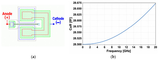
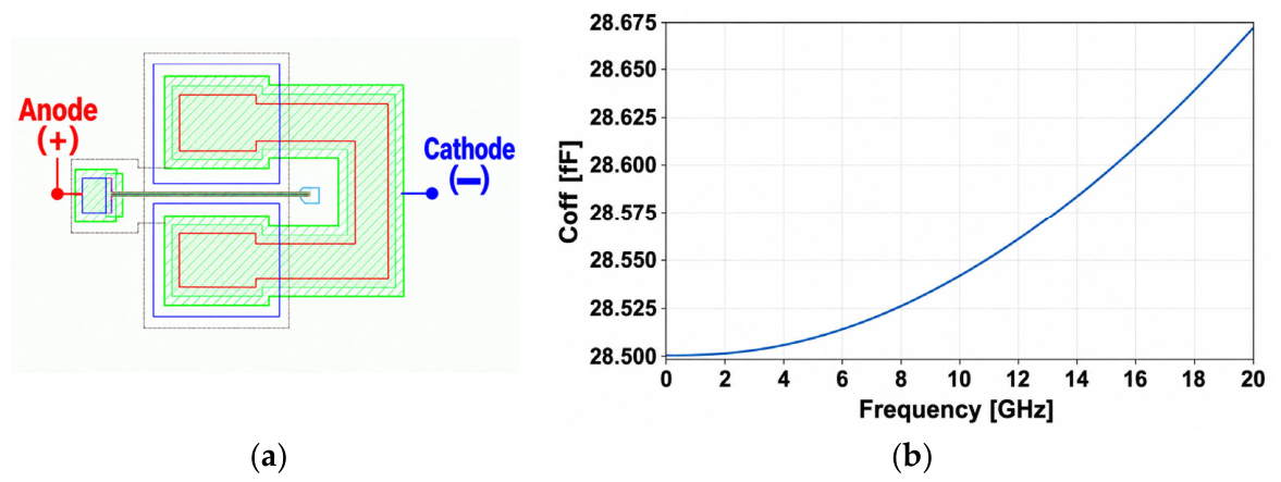
A standard Schottky barrier diode (SBD) with a unit size of 0.1 × 10 μm2 was selected for the circuit design. This diode is a standard active device provided by the WIN Semiconductors 0.1-μm GaAs D-mode pHEMT process. In the OFF state, the insertion loss is governed by (1), where is the characteristic impedance, is the operating frequency, is the OFF-state capacitance, and Rs is the parasitic series resistance of the diode [8,9]. Since insertion loss scales with , keeping small is the primary lever for maintaining low insertion loss across a wide band. The 0.1 × 10 µm2 unit cell offers the smallest available in the process. This comes at the cost of a higher Ron and thus reduced power-handling capability [8]. Figure 1a illustrates the layout of the utilized 0.1 × 10 μm2 standard SBD. The OFF-state capacitance () of this device was extracted from small-signal simulation of the SBD unit cell in the OFF state. As shown in Figure 1b, remains approximately 28.5 fF across the target 6–18 GHz range, confirming stable capacitance characteristics suitable for broadband limiter design.
Figure 1.
Layout and simulated OFF-state capacitance of the 0.1 × 10 μm2 native SBD in 0.1-μm GaAs pHEMT process: (a) diode layout and (b) simulated versus frequency.
2.2. Circuit Topology
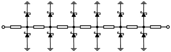
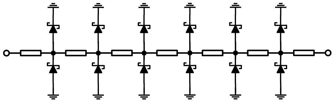
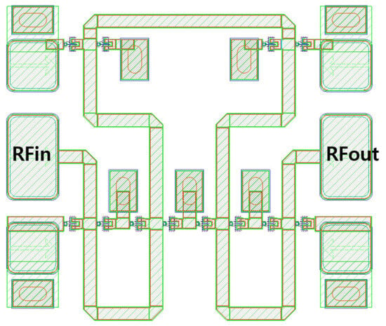
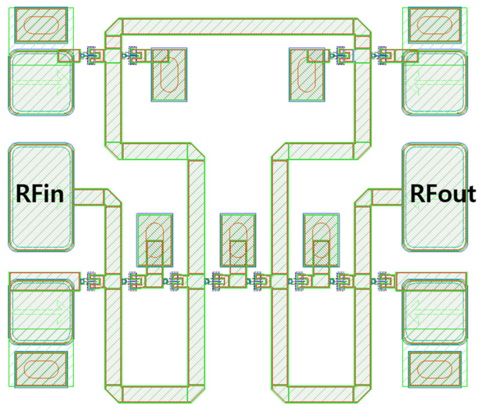
As illustrated in Figure 2, the proposed limiter employs an anti-parallel, single-stack Schottky diode configuration arranged in a six-stage cascaded topology. The corresponding chip layout is shown in Figure 3. The anti-parallel connection is essential to symmetrically clip both the positive and negative half-cycles of the incident high-power RF signals, thereby minimizing the generation of unwanted even-order harmonics. In this design, a single stack diode configuration per branch is employed rather than a multi stacked series structure. While stacking multiple diodes in series can improve the overall power-handling capability, it also proportionally increases the effective turn-on voltage, resulting in a higher threshold power level. Therefore, the one-stack configuration is implemented to ensure that the limiter activates at a lower input power level. Furthermore, the single stack diode configuration reduces the carrier storage effect at each junction, contributing to a faster recovery response compared with multi-stacked configurations.
Figure 2.
Schematic diagram of the proposed six-stage anti-parallel Schottky diode limiter.
Figure 3.
Layout of the proposed six-stage anti-parallel Schottky diode limiter.
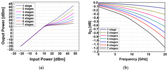
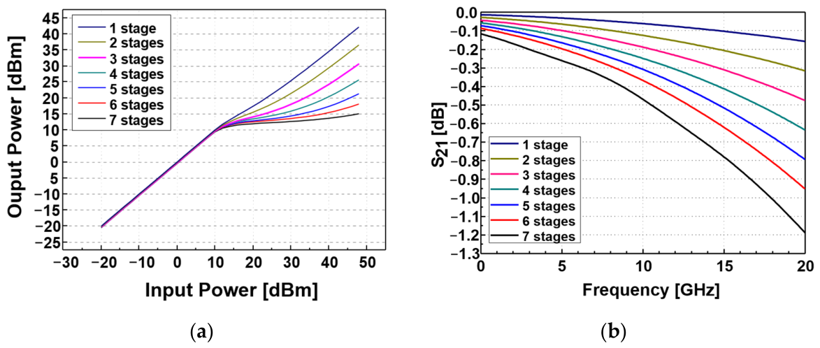
However, a single-stage single-stack SBD fails to sufficiently suppress high-power injection, resulting in an unflattened leakage response. To determine the appropriate number of stages, parametric simulations were performed using Keysight ADS 2025 across one- to seven-stage configurations, evaluating the trade-off between limiting flatness and small-signal insertion loss. As illustrated in Figure 4a, as the number of stages increases, the limiting flatness progressively improves. Furthermore, an even number of stages is adopted to enable a symmetrical layout architecture, improving spatial efficiency within the chip area. Therefore, the six-stage configuration is selected, as it is the minimum even-numbered stage that simultaneously achieves a flat leakage power below 15.5 dBm and an insertion loss of less than 1 dB across 6–18 GHz. Although the seven-stage configuration offers marginally improved limiting flatness, the associated increase in insertion loss beyond 1 dB, as shown in Figure 4b, makes it unsuitable for the target application.
Figure 4.
Simulated performance comparison of one- to seven-stage cascaded SBD limiter topologies: (a) output power versus input power at 12 GHz, and (b) small-signal insertion loss (S21) versus frequency.
2.3. Compact Layout Implementation
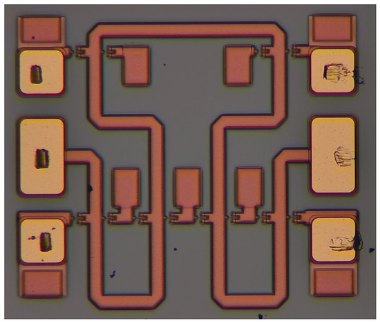
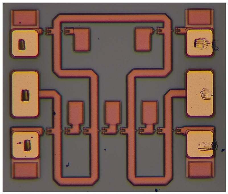
In GaAs MMIC manufacturing, the physical footprint of the chip is a primary factor determining the overall fabrication cost. Although the proposed six-stage topology significantly enhances the power-limiting capability, placing six cascaded diode stages with conventional straight microstrip transmission lines would inevitably result in an excessively long chip layout, reducing the number of dies per wafer. To overcome this layout constraint, a symmetrical layout architecture was adopted by selecting an even number of cascaded stages, which improves area efficiency. Within this arrangement, the inter-stage transmission lines were folded into compact meander-line structures. The inter-stage meander lines and shunt-connected SBDs form an artificial transmission line. The meander line provides series inductance, and the SBD provides shunt capacitance in its OFF state. The diode’s OFF-state capacitance is thus part of the propagation structure by design. Each section was sized to present a 50 Ω characteristic impedance, determined from the extracted Coff of 28.5 fF. The inter-stage meander line has a length of 450 μm and a width of 30 μm, and the values were selected through parametric EM simulation as the optimal values that simultaneously satisfy the impedance matching condition and the series inductance requirement within the compact layout footprint. A wider line reduces the series inductance per unit length, requiring a longer line to provide the same inductance and thereby increasing the layout area. The 30 μm width was therefore selected as a compromise between the required series inductance and the compact layout footprint. To further reduce the core area, ground-via sharing was implemented. Consequently, the entire limiter MMIC, including the measurement pads, was implemented in a size of 0.80 × 0.69 mm2 (Figure 5).
Figure 5.
Chip microphotograph of the fabricated six-stage SBD Limiter. The total chip area, including the RF measurement pads, is compact at .
3. Measurement Results
3.1. Small-Signal Performance
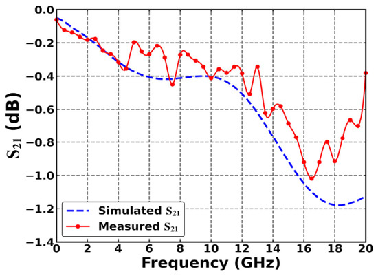
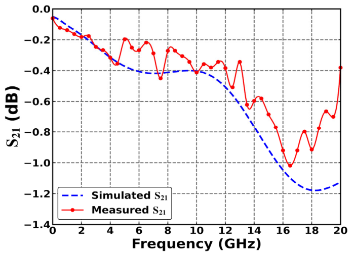
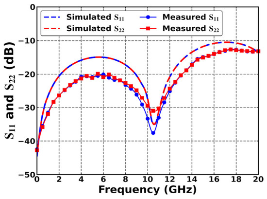
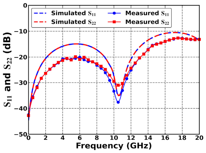
Small-signal S-parameters were measured on-wafer using an RF probe station and ground-signal-ground (GSG) probes. S-parameters were acquired using an Anritsu MS46122B ShockLine vector network analyzer (VNA, Anritsu Company, Morgan Hill, CA, USA). Prior to measurement, short-open-load-through (SOLT) calibration was performed at the probe tips to establish the reference planes at the device ports. As shown in Figure 6, the measured insertion loss remains below 1.01 dB across the entire 6–18 GHz operating band. Figure 7 shows the measured results are in good agreement with the simulated results.
Figure 6.
Simulated and measured small-signal insertion loss ( versus frequency.
Figure 7.
Simulated and measured small-signal return loss ( versus frequency.
Cascading multiple diode stages introduce cumulative parasitic capacitance and series resistance, which tend to degrade transmission performance at higher frequencies [10,11]. In the proposed single stack six-stage topology, the inter-stage meander lines behave as series inductors. Together with the off-state shunt capacitance of the SBDs, they form a periodic LC ladder network that behaves as an artificial transmission line. This distributed LC structure maintains a stable characteristic impedance across the operating band, thereby mitigating the insertion loss degradation associated with cascading multiple limiter stages. Consequently, the proposed limiter maintains broadband impedance matching across the entire 6–18 GHz operating band, as confirmed by the measured results.
3.2. Large-Signal Limiting Performance
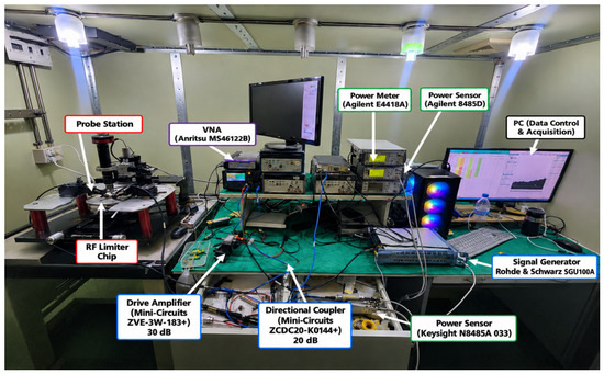
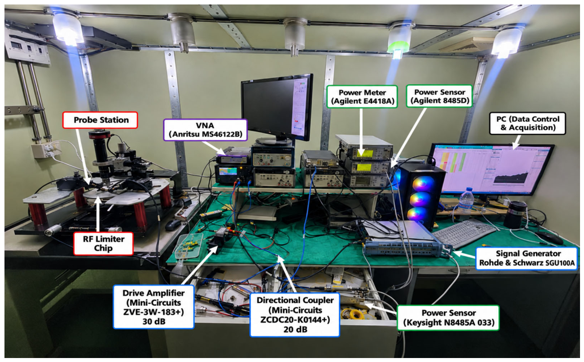
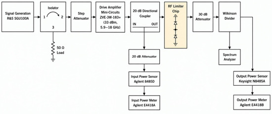
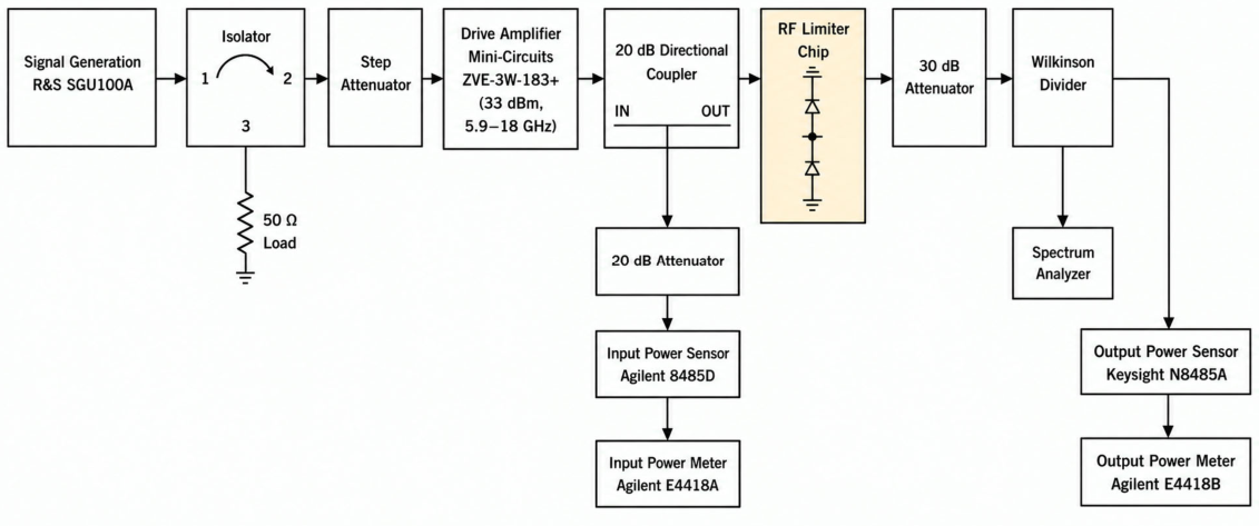
The large-signal measurement setup is illustrated in Figure 8 and Figure 9. The continuous-wave (CW) input signal was generated using a Rohde & Schwarz SGU100A signal source (Rohde & Schwarz GmbH & Co. KG, Munich, Germany). The signal then passed through an isolator, followed by a step attenuator and a 33-dBm drive amplifier (Mini-Circuits ZVE-3W-183+, Brooklyn, NY, USA). The amplified signal was applied to the RF limiter through a 20-dB directional coupler. The incident power was monitored from the coupled port using an Agilent E4418A power meter (Agilent Technologies, UK). At the output, the transmitted power was measured at the output port of a 3-dB coupler using an Agilent E4418B power meter (Agilent Technologies, Oxford, UK). The other port of the 3-dB coupler was connected to a Signal Hound SM435B spectrum analyzer (Signal Hound, Battle Ground, WA, USA) for spectral monitoring. To evaluate the power-limiting capabilities of the fabricated MMIC, large-signal continuous-wave (CW) power sweep measurements were conducted across 6–18 GHz in 1 GHz steps.
Figure 8.
Photograph of the large-signal CW power sweep measurement setup for the fabricated RF limiter MMIC.
Figure 9.
Block diagram of the large-signal CW power sweep measurement setup.
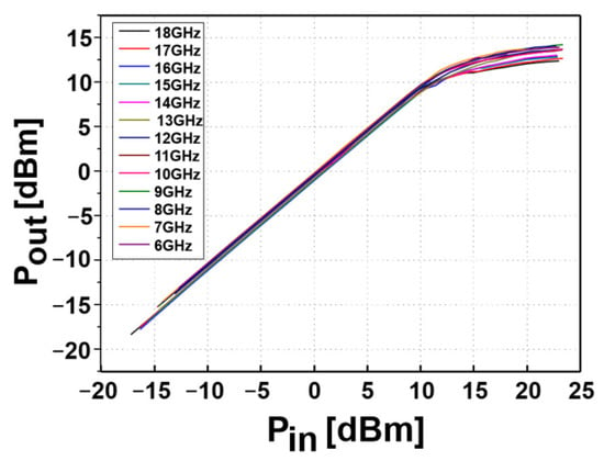
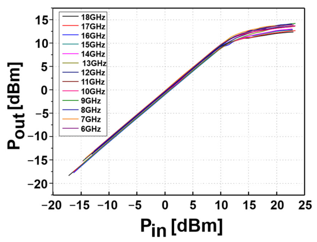
As illustrated in Figure 10, the measured output power versus input power confirms the broadband uniformity of the limiting response. The incident RF power was swept from the linear small-signal region up to 23 dBm.
Figure 10.
Measured output power () versus input power ().
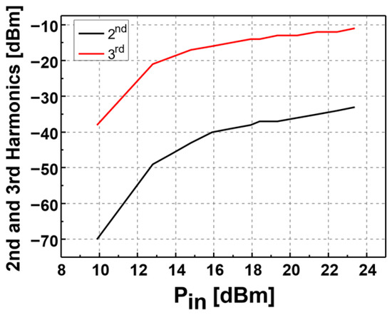
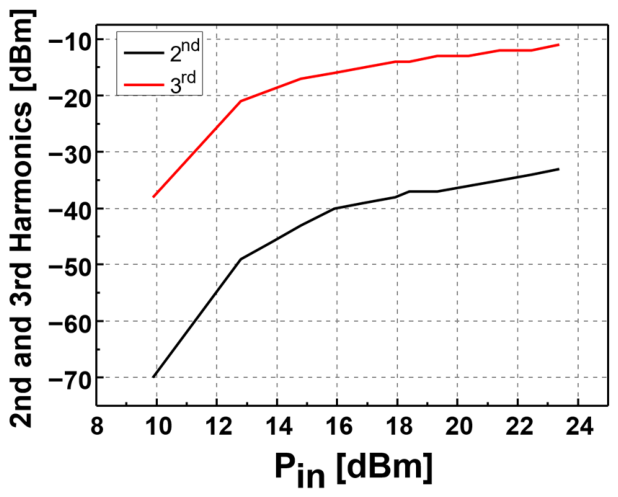
Unlike a single-stage design, which provides limited output suppression as input power rises, the cascaded multi-stage configuration progressively clips the signal and clamps the output to a flat leakage level below 14.2 dBm at the maximum tested input of 23 dBm. This flat limiting characteristic is maintained across the entire 6–18 GHz band with minimal frequency dependence, as seen in Figure 10. Spectral monitoring via the Signal Hound SM435B revealed the onset of harmonic distortion at input power levels of 10–24 dBm (Figure 11). At the input power over 10 dBm, the third-order harmonic component exceeded the second-order harmonic in power. This is consistent with the symmetric clipping produced by the anti-parallel SBD topology, in which even-order harmonics are inherently suppressed relative to odd-order components, confirming that the observed output compression is driven by this symmetric limiting mechanism. The limiter was characterized up to an input power of 23 dBm. During the measurement, it was observed that when maximum input power exceeded approximately 25.2 dBm, the limiter was permanently damaged. Several recently reported RF limiters are capable of withstanding input power levels exceeding 30 dBm [11,12]. Such high-power capability is commonly achieved by employing larger diode peripheries, which reduce the series resistance and allow for higher current conduction. However, the accompanying increase in junction capacitance leads to higher insertion loss. Alternatively, multi-diode power-splitting networks can be employed to distribute the incident power. However, this approach substantially increases the chip area and circuit complexity, and the larger total junction capacitance tends to increase the recovery time.
Figure 11.
Measured 2nd- and 3rd-order harmonic power versus input power at 12 GHz.
3.3. Recovery Time Measurement
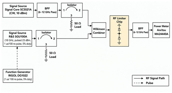
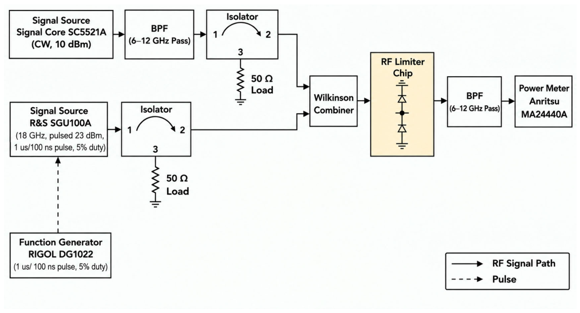
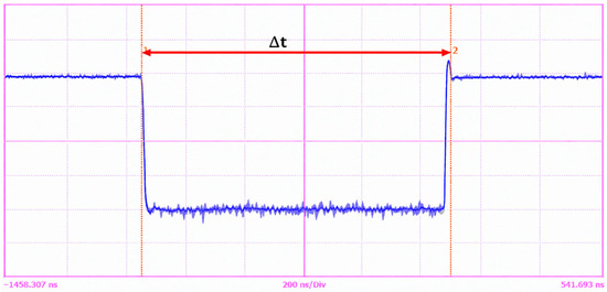
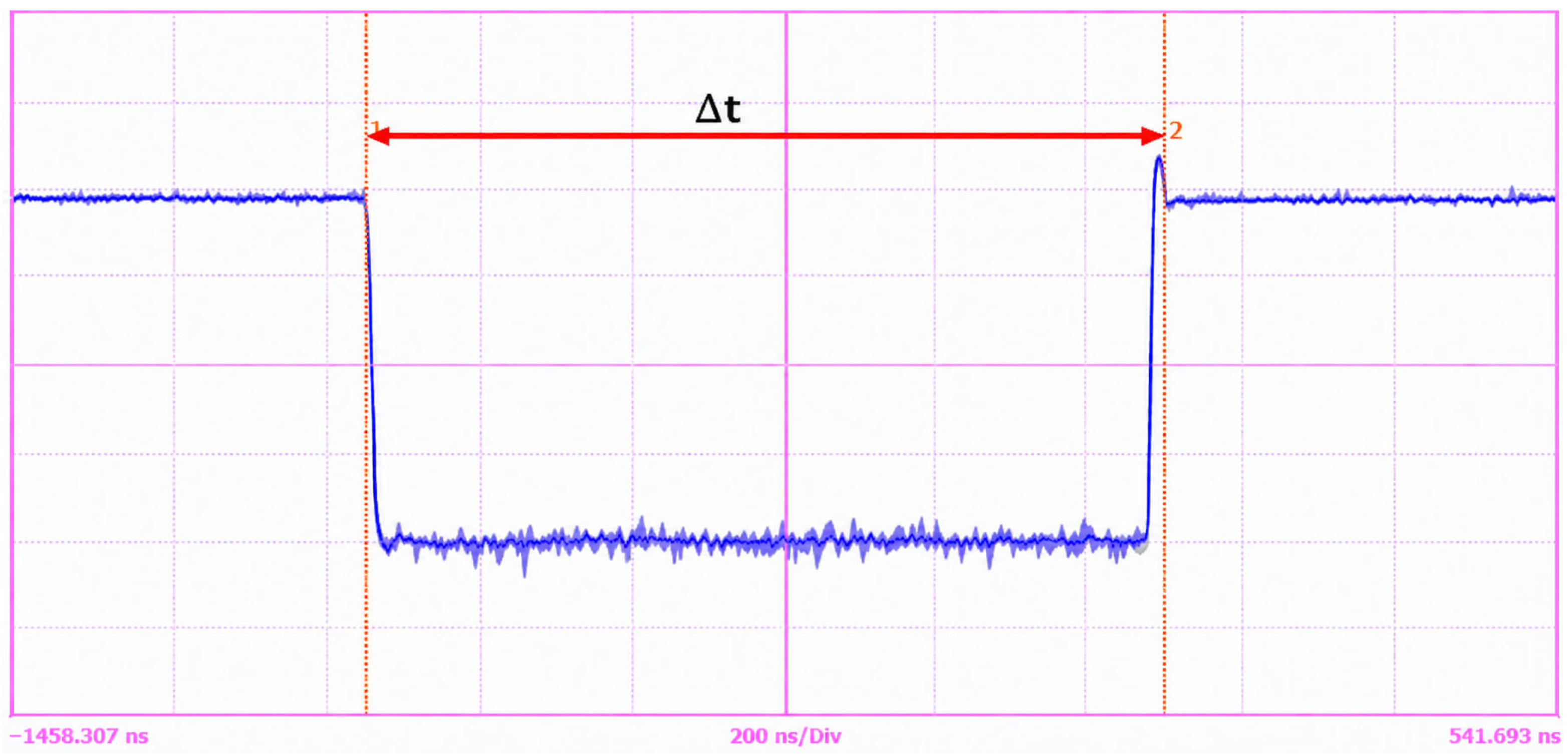
The recovery time is the time it takes for the device to return to its normal, low-loss state after a large high-power signal stops [13,14]. The measurement setup is shown in Figure 12. Two signals at distinct frequencies are applied simultaneously to the limiter under test through a Wilkinson combiner: a continuous-wave (CW) signal and an 18 GHz pulsed interfering signal. The CW signal has 10 dBm, and the pulse signal has 23 dBm. To verify that the recovery performance is maintained across the operating band, the CW signal frequency is swept from 6 to 12 GHz in 1 GHz steps, yielding seven frequency combinations with the fixed 18 GHz interfering pulse. The 18 GHz pulse is applied at two pulse widths (PW), 1 µs and 100 ns, both at a 5% duty cycle, and is controlled by a function generator. Under normal operation, the small CW signal passes through the limiter with low insertion loss. When the 18 GHz large pulse is applied, the internal Schottky diodes conduct, placing the limiter in saturation, and the limiter gets high insertion loss. Conventionally, the recovery time is measured at the falling edge after the high-power pulse disappears [13]. However, due to the ambiguity of the falling edge with short time, we tried to measure it with negative pulse width instead. We applied a 6–12 GHz band-pass filter (Mini-Circuits ZBSS-9G-S+, Brooklyn, NY, USA), which has a 6 to 12 GHz pass band and 90 dB rejection at 18 GHz, in front of the output power meter, as shown in Figure 12. Then the 18 GHz pulse is removed, and we only see the CW signal power at the power meter. In the pulse measurement of the power meter, we see low CW signal power while the 18 GHz pulse exists and high CW power while the 18 GHz pulse disappears, as shown in Figure 13. The negative pulse width includes the 18 GHz pulse and the recovery time of the limiter. Therefore, the recovery time is obtained from:
where Δt is the measured negative pulse width and PW is the 18 GHz interfering pulse width. is extracted between the outermost transition points of the falling and rising edges. The measurements are performed using an Anritsu MA24440A peak power sensor (Anritsu Company, Morgan Hill, CA, USA), which provides a temporal resolution of 100 ps. As summarized in Table 1, the recovery time remains within 39–43.2 ns across all seven frequency combinations and both pulse widths.
Figure 12.
Block diagram of the two-tone recovery time measurement setup.
Figure 13.
Measured negative pulse width from the CW signal and 18 GHz pulse signal.
Table 1.
Measured recovery time for CW signal frequencies of 6–12 GHz with an 18 GHz interfering pulse.
The performance of the proposed limiter is summarized and compared with the other SBD limiters in Table 2. As summarized in Table 2, the proposed design occupies the smallest area, low insertion loss, and recovery time.
Table 2.
Performance comparison of SBD-based RF limiters.
4. Conclusions
In this paper, a broadband microwave limiter MMIC fabricated using the WIN Semiconductors 0.1-μm GaAs D-mode pHEMT process is presented. The process provides a monolithic integration that combines the Schottky barrier diode with transmission line elements on a single chip, avoiding the assembly tolerances and additional parasitic components associated with hybrid implementations. By employing a cascaded six-stage Schottky barrier diode (SBD) topology with optimized inter-stage meander transmission lines, the proposed limiter achieves a compact chip size and wide bandwidth operation. The meander lines contribute series inductance that, together with the diode off-state capacitance, forms an artificial transmission line through which consistent impedance characteristics are maintained across the operating band without additional matching networks. The measurement results confirm a small-signal insertion loss below 1.01 dB, a return loss better than 12 dB, and a flat leakage power below 14.2 dBm across the entire 6–18 GHz band, with a maximum input power of 25.2 dBm and a recovery time below 43.2 ns. The key contribution of this work lies in demonstrating that compact MMIC integration with low insertion loss and effective wideband limiting can be simultaneously achieved within a standard GaAs pHEMT process, without requiring additional epitaxial steps, matching networks, or multi-diode power-splitting structures.
Author Contributions
Conceptualization, M.S. and D.-H.L.; investigation, M.S., J.L. and G.J.; formal analysis, M.S.; writing—original draft preparation, M.S.; writing—review and editing, J.L., G.J. and D.-H.L.; and supervision, G.J. and D.-H.L. All authors have read and agreed to the published version of the manuscript.
Funding
This work was supported by Jeollanam-do, South Korea and carried out as part of the MPW support project at the Compound Semiconductor Research Center (CSRC), under the “Region-based Project for Technical Support and Manpower Development in Compound Semiconductors (2025-0012)”. This work was supported by the Institute of Information & Communications Technology Planning & Evaluation (IITP) grant funded by the Korean government (MSIT) (No. RS-2024-00400864, Development of Upper-mid Band E-MIMO Base Station Antenna Beamforming Module).
Data Availability Statement
The data presented in this study are available on request from the corresponding authors. The data are not publicly available due to proprietary research infrastructure and confidentiality agreements.
Conflicts of Interest
The authors declare no conflicts of interest.
References
- Li, S.; Ma, L.; Wang, L.; Lei, X.; Wu, B.; Cheng, G.; Liu, F. High Power 10–18 GHz Monolithic Limiter Based on GaAs p-i-n Technology. IEEE Microw. Wirel. Compon. Lett. 2022, 32, 1107–1110. [Google Scholar] [CrossRef] [Scilit]
- Kyabaggu, P.B.K.; Haris, N.; Rezazadeh, A.A.; Sinulingga, E.; Alim, M.A.; Zhang, Y. Design and realisation of a pHEMT Diode MMIC Power Limiter Using 3D GaAs Multilayer CPW Technology. In Proceedings of the 45th European Microwave Conference (EuMC), Paris, France, 7–10 September 2015; pp. 522–525. [Google Scholar] [CrossRef] [Scilit]
- Mini-Circuits. RLM-63-2W. Available online: https://www.minicircuits.com (accessed on 3 June 2026).
- Maas, A.P.M.; Janssen, J.P.B.; van Vliet, F.E. Set of X-Band Distributed Absorptive Limiter GaAs MMICs. In Proceedings of the 4th European Radar Conference (EuRAD), Munich, Germany, 10–12 October 2007; pp. 17–20. [Google Scholar] [CrossRef] [Scilit]
- Pham, B.L.; Nguyen, D.P.; Pham, A.-V.; Le, P.D. High Power Monolithic pHEMT GaAs Limiter for T/R Module. In Proceedings of the 2016 IEEE Compound Semiconductor Integrated Circuit Symposium (CSICS), Austin, TX, USA, 23–26 October 2016; pp. 1–4. [Google Scholar] [CrossRef] [Scilit]
- Grusha, A.V.; Rebrov, A.S. MMIC GaAs Power Limiter on 30 GHz with a Small Flat Leakage Power. In Proceedings of the 2023 IEEE 16th International Conference of Actual Problems of Electronic Instrument Engineering (APEIE), Novosibirsk, Russia, 10–12 November 2023; pp. 130–133. [Google Scholar] [CrossRef] [Scilit]
- Zhu, H.-R.; Wang, J.; Tang, M. Compact, High Power Capacity, and Low Insertion Loss Millimeter-Wave On-Chip Limiting Filter with GaAs PIN Technology. IEEE Trans. Circuits Syst. I Regul. Pap. 2023, 70, 1175–1188. [Google Scholar] [CrossRef] [Scilit]
- Zhu, H.-R.; Wang, J. Miniaturized, Ultrawideband and Low Insertion Loss Ku-Band GaAs On-Chip Limiter by Improved π-Type Topology with Capacitive Loading. IEEE Trans. Electron Devices 2023, 70, 971–978. [Google Scholar] [CrossRef] [Scilit]
- Wanum, M.; Vliet, F.E. A 58-dBm S-Band Limiter in Standard 0.25-μm BiCMOS Technology. IEEE Trans. Microw. Theory Tech. 2013, 61, 3034–3042. [Google Scholar] [CrossRef] [Scilit]
- Zhao, R.; Kang, X.; Zheng, Y.; Wu, H.; Gao, J.; Wei, K.; Liu, X. High-Power Microwave Limiters Using Recess-Free AlGaN/GaN Schottky Barrier Diodes. IEEE Microw. Wirel. Technol. Lett. 2023, 33, 208–211. [Google Scholar] [CrossRef] [Scilit]
- Sun, Y.; Dun, S.; Zhang, D.; Yin, Z.; Zhao, S.; Ruan, P.; Huang, S.; Wei, K.; Liu, X. First Demonstration of L-Band High-Power Limiter with GaN Schottky Barrier Diodes (SBDs) Based on Steep-Mesa Technology. Electronics 2021, 10, 433. [Google Scholar] [CrossRef] [Scilit]
- Zhao, R.; Kang, X.; Zheng, Y.; Wu, H.; Huang, Y.; Sun, Y.; Deng, S.; Wei, K.; Liu, X. High-Power GaN SBD Limiter for Sub-6G with Fast Response and Recovery. IEEE Microw. Wirel. Technol. Lett. 2024, 34, 57–60. [Google Scholar] [CrossRef] [Scilit]
- Zhao, R.; Kang, X.; Zheng, Y.; Wu, H.; Gao, J.; Wei, K.; Liu, X. Fast Recovery Performance and Design Method for High-Power Microwave Limiter Using GaN-SBD Technology. IEEE Trans. Microw. Theory Tech. 2024, 72, 4822–4832. [Google Scholar] [CrossRef] [Scilit]
- Looney, J.; Conway, D.; Bahl, I. An examination of recovery time of an integrated limiter/LNA. IEEE Microw. Mag. 2004, 5, 83–86. [Google Scholar] [CrossRef]

Disclaimer/Publisher’s Note: The statements, opinions and data contained in all publications are solely those of the individual author(s) and contributor(s) and not of MDPI and/or the editor(s). MDPI and/or the editor(s) disclaim responsibility for any injury to people or property resulting from any ideas, methods, instructions or products referred to in the content. |
© 2026 by the authors. Licensee MDPI, Basel, Switzerland. This article is an open access article distributed under the terms and conditions of the Creative Commons Attribution (CC BY) license.