


Abstract
This paper presents a nonlinear control scheme for regulating the output voltage of a high-gain active switched-inductor boost converter. The proposed converter topology extends the conventional boost converter by incorporating an additional inductor and a power semiconductor device, thereby enhancing the voltage conversion ratio. The control objectives are twofold: precise regulation of the output voltage and stabilization of the inductor current. To achieve these goals, an interconnection and damping assignment passivity-based control strategy is developed. A dynamic extension is further introduced to compensate for steady-state errors caused by unmodeled parasitic resistances in the system components. In addition, a reference current generator with proportional–integral action is implemented to provide an appropriate current reference. The effectiveness of the proposed controller is validated both numerically and experimentally under three operating scenarios: load step changes, input voltage variations, and output voltage reference transitions.
1. Introduction
The electrical industrial sector has been motivated to increase the integration of renewable energy due to the high environmental effects brought on by the excessive use of pollutant energy sources like oil, coal, and natural gas. Conditioning and storing energy generated by renewable sources is crucial; however, the output voltage from the vast majority of renewable sources is low and uncontrolled, meaning that it cannot be utilized in a wide range of applications. For this reason, the adoption of renewable energies at domestic and industrial levels requires the development of power electronic systems as well as control strategies to operate under reliable conditions [1].
The well-known DC-DC boost converter (BC) is a functional topology for increasing the output voltage of DC renewable sources such as photovoltaic (PV) and fuel cell (FC) systems; however, the BC’s low efficiency for a high-duty ratio results in a limited voltage boost for applications dealing with high output power [2]. A solution to this problem involves employing transformerless high-gain BCs that use voltage-boosting techniques [3], such as switched capacitors (charge pump) [4], switched-inductor networks [5], voltage multiplier cells [6], voltage lift techniques [7], magnetic coupling [8], and multistage converters [2]. These high-gain non-isolated converters are low cost, energy efficient, and compact compared to converters with high-frequency transformers. Moreover, to further enhance the voltage conversion ratio, some combinations of these voltage-boosting techniques can be implemented, such as switched inductors with switched capacitors [9], switched inductors with magnetic coupling [10], and switched inductors with voltage lift [11].
For instance, in [5], three active switched-inductor (ASL) BCs are presented. The structure of these ASL converters is based on the conventional BC; however, the main difference is that an inductor and a power semiconductor device have been added to the topology, which enhances the conversion ratio of the output voltage while keeping a duty cycle within acceptable limits when compared with the conventional BC. Some advantages of these ASL-BC are low-voltage stress in semiconductors, high-voltage gain, and the use of equal-value inductors to simplify the analysis. Additionally, from a dynamic performance and feedback point of view, topologies focused on renewable energy require advanced control schemes that regulate the output voltage, achieve current tracking for a secure operation, and even mitigate the effect of uncertainties and disturbances. In addition, power converters with boosting capability exhibit a non-minimum phase behavior of the output voltage with respect to the duty cycle, which may cause instability and poor dynamic performance. These challenges are effectively addressed by the well-known current-mode control (CMC) where the output voltage is driven by a direct control of the inductor current. To this end, CMC employs a multi-loop control strategy in which the inner loop is dedicated to current regulation and the outer loop is responsible for output voltage control. From a stability standpoint, both loops can be designed independently, each admitting its own stability proof. Several control strategies have been reported in the literature, regarding CMC. For example, ref. [12] uses classical control theory to design a CMC switching regulator by using a quadratic BC to operate an FC system. In this case, the inner loop is based on a high-gain compensator, and the outer loop uses a proportional–integral (PI) controller. Furthermore, in [13], for the high-gain ASL-BC considered in this work as well, three controllers based on multi-loop PI actions are designed and experimentally validated. These controllers use the time-scale separation principle between the current and voltage dynamics to construct independent inner and outer loops which simplifies the control design stage. However, this approach does not provide formal stability guarantees, as no rigorous stability proof is offered for either the inner or outer loop. Furthermore, a CMC considering Euler–Lagrange (EL) standard passivity-based control (PBC) and a PI action for the inner and outer loops, respectively, is detailed in [14,15], to control a double-inductor BC and an FC/BC system, respectively. However, this approach requires the online solution of four additional differential equations to reconstruct the parasitic parameters and compute the control signal. In particular, the PBC approach has been widely used to control power electronics [16,17,18,19] due to its main characteristic: reformulation of energy balancing, i.e., system energy can be driven to a desired energy level. Under this idea, three main branches have been reported: EL standard PBC [20], and PBC for port-controlled Hamiltonian (PCH) systems, which in turn can be divided into interconnection and damping assignment (IDA) [21] and PI-PBC [22]. The IDA-PBC control approach has been considered in several applications such as DC microgrid systems [23,24], robotics, mechanical and electromechanical systems [25,26,27,28,29], and for power conversion [30,31,32,33]. Explicitly, the IDA-PBC approach is based on assigning a desired energy function, interconnection, and damping using the control input. Different from other nonlinear control strategies that focus on the signal approach, IDA-PBC exploits the physical structure and considers the energy relationship of the system to design stabilizing control laws with practical feasibility [32]. Thus, this work details the design of a nonlinear control scheme under CMC to regulate the output voltage of a high-gain ASL BC. The IDA-PBC strategy is developed for the inner current loop, while a model-based reference current generator (RCG) to provide the current reference is designed as an outer voltage loop. In addition, a dynamic extension is constructed to cope with the parasitic effects of the converter, such as the non-modeled inductor resistance and parameter uncertainty, thus eliminating steady-state error. The following are the main contributions of this research regarding the output voltage regulation of the ASL-BC system:
- The port-controlled Hamiltonian formulation for the ASL-BC.
- The nonlinear control scheme design for the ASL-BC is based on interconnection and damping assignment passivity-based control (IDA-PBC) with an integral action to eliminate the effect of non-modeled parasitic resistances and parameter uncertainty in the system. No restrictions are imposed over the control tuning gains, nor does the control law exhibit singularities; therefore, asymptotic stability is ensured for the operation range of the ASL-BC.
- The combination of a nonlinear control strategy for the inner current loop and a model-based reference current generator to avoid an intricate approximation of the system equilibrium. This approach requires the online solution of only two additional differential equations to compute the duty cycle.
- Numerical and experimental validation of the closed-loop system under several scenarios.
The rest of the paper is organized as follows: In Section 2, the operation and modeling of the ASL-BC in the PCH formulation approach are analyzed. Section 3 details the design of the proposed IDA-PBC controller along with the dynamic extension. Section 4 shows the evaluation of the proposed control law with numerical and experimental results. Finally, Section 5 addresses the conclusion and future work.
2. System Description
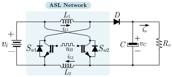
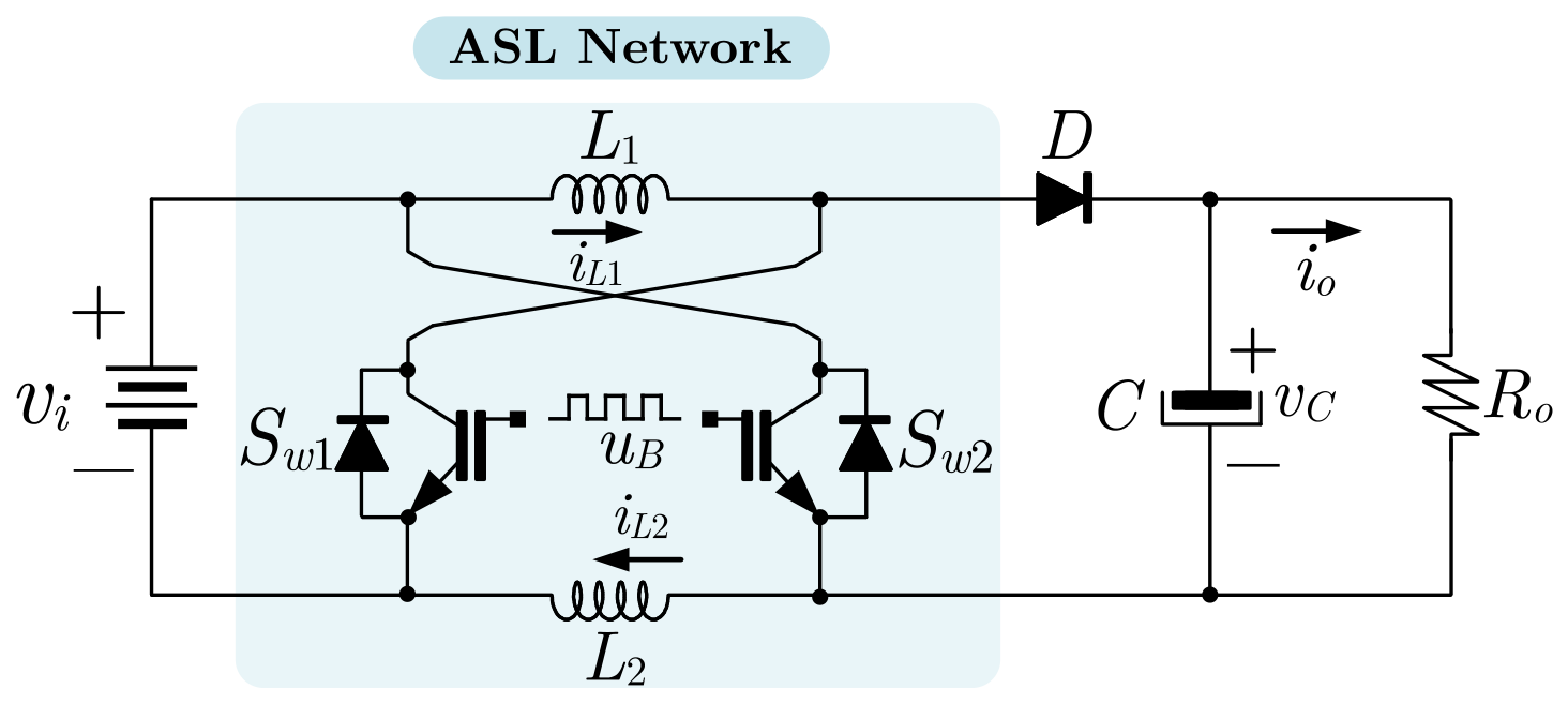
The ASL-BC under study is shown in Figure 1. The topology consists of a DC source used as a power supply to the converter, the ASL network formed by two active switches and that operate in synchrony, and inductors and . This switching array allows the inductors to be charged in parallel and discharged in series. Additionally, a diode D, an output capacitor C, and a resistor used to model the output nominal load are considered. By virtue of its topology, the ASL-BC achieves a high voltage conversion ratio without requiring an extreme duty cycle, making it particularly suitable for applications such as fuel cell systems, photovoltaic systems, and other energy conversion systems that demand a high DC-DC step-up voltage gain [5].
Figure 1.
ASL-BC configuration.
Remark 1.
Assumptions 1–3 represent standard idealizations commonly adopted in the passivity-based control literature for power converters [34], yielding a tractable averaged model while preserving the essential dynamic behavior for control design. The unmodeled parasitic resistances in 2–3 motivate the dynamic extension, which compensates for the resulting steady-state error without requiring explicit knowledge of their values, as demonstrated in Section 4. Regarding 1, unknown stepwise changes in are explicitly considered in Scenario ii. More generally, the integral action converges to a non-zero steady-state value that offsets any unmodeled constant parameters or disturbances, as established in Proposition 1.
To define the physical dynamical behavior of the ASL-BC, it is necessary to consider the following idealizing assumptions:
Assumption 1.
The input voltage source is considered ideal, i.e., provides a constant voltage.
Assumption 2.
The semiconductors , , and the diode D are considered energy lossless.
Assumption 3.
Energy losses in inductors due to unknown constant parasitic resistances are not considered in the average system model; however, real-world parasitics are compensated by the dynamic extension proposed in this work.
Assumption 4.
The continuous conduction mode (CCM) is considered for the physical operation of the system. This mode means that the inductor current never reaches zero value during operation. The discontinuous conduction mode (DCM), which is when the inductor current reaches zero value during operation, is not considered due to the high input current ripple that may affect the power supply [5].
Assumption 5.
Furthermore, , , C, and are known constant parameters.
As a result of the synchronous operation of the active switches and , the operation of the ASL-BC is described as follows. During turn ON mode the switches are activated, and the inductors are charged in parallel. The stored energy in the capacitor C is delivered to the load . Consequently, the diode D is reverse-biased and therefore isolates the load from the power supply. During turn OFF mode the switches are disabled, and the stored energy in the inductors is discharged in series to the capacitor C. Since the diode D is forward-biased, it allows current to circulate from the inductors and source to the nominal load . Consequently, based on the operation modes described above and Kirchhoff’s current and voltage laws, the dynamic average model of the system is determined as
where is the state vector of the system. Note that and represent the current flowing through inductors and and the output capacitor voltage, respectively. The input control u indicates the duty cycle to trigger the active switches through a PWM function. As seen in Figure 1, three energy storage devices are observed; therefore, a third-order model can be expected. However, considering , it is possible to reduce the order of the system from third to second. Consequently, the current dynamics in (1) presents the time constant . In addition, it is assumed all state variables are measurable. Furthermore, coherent with the physical meaning, x and the control signal u are considered to be bounded from below to ensure CCM and from above for safety reasons. In steady state, considering that the control signal remains constant, i.e., , the equilibrium points of (1) are found to be
It is worth noting that the ASL-BC topology achieves a higher voltage conversion ratio than both the conventional BC and the interleaved boost converter, which are limited to a ratio of , while the ASL-BC attains this enhancement by simply incorporating an additional switched-inductor branch into the conventional topology.
Remark 2.
To compute the equilibrium point for the inductor current, complete knowledge of the load resistance is required, which is subject to unknown variations in practice. Additionally, as presented in [5,14,35], the transfer function relating the output voltage to the control signal exhibits a non-minimum phase behavior; therefore, implementing a controller to regulate the output voltage directly is not suitable, since it may cause instability; instead, a CMC is preferred.
In order to design an IDA-PBC control scheme for the inner current loop, the physical behavior of the plant shown in Figure 1 is reformulated based on PCH systems as
where represent a skew-symmetry interconnection matrix containing the passive elements that store energy in the system, and the matrix refers to the dissipation matrix that contains the dissipating components, such as the nominal load . The Hamiltonian (energy) function is represented by and consequently . The port characteristic matrix of the converter is denoted by , and is the input or disturbance vector. In this case, the associated matrices to (3) for the ASL-BC are defined as
The Hamiltonian function of the ASL-BC is selected as the sum of the inductors and capacitor energy as
and consequently the partial derivative of the energy with respect to the state is
Problem formulation: Consider that the ASL-BC given in (3) fulfills Assumptions 1–5. It is required to design a dynamic state feedback control strategy such that the equilibrium of the extended inner closed-loop system is asymptotically stable.
In the following section, an IDA-PBC design with an integral action is detailed to operate the ASL-BC ensuring current tracking and output voltage regulation in the presence of parasitic, non-modeled resistances and capable of facing input voltage and load variations.
3. IDA-PBC Control Scheme Design
The main idea of the IDA-PBC strategy, based on PCH systems, is presented in [21] and relies on the designation of a desired storage energy function , with a desired fixed equilibrium point, interconnection, and damping assignment via feedback. To ensure system stability, the desired energy storage function must have a minimum at the desired equilibrium point. Additionally, the damping assignment is performed through virtual resistances, which dissipate energy and impose the convergence rate to the desired point. Furthermore, the ideas above can be extended with an integral action to eliminate model errors while preserving the stability of the closed-loop system [36]. In this section, the design of an IDA-PBC scheme law is proposed for the inner current loop to generate the duty cycle for the ASL-BC, and then, a model-based reference current generator is implemented to provide a current reference to be tracked by the inner loop. Moreover, for the ASL-BC operating in a closed loop, the control objectives are described in detail below.
- 1.
- Input inductor current tracking to a desired reference current , i.e.,where the desired current value is obtained from the model-based reference current generator.
- 2.
- Output voltage regulation to a desired reference valuewhere the reference voltage desired value is defined by the nominal operation of the ASL-BC.
3.1. IDA-PBC Inner Current Loop
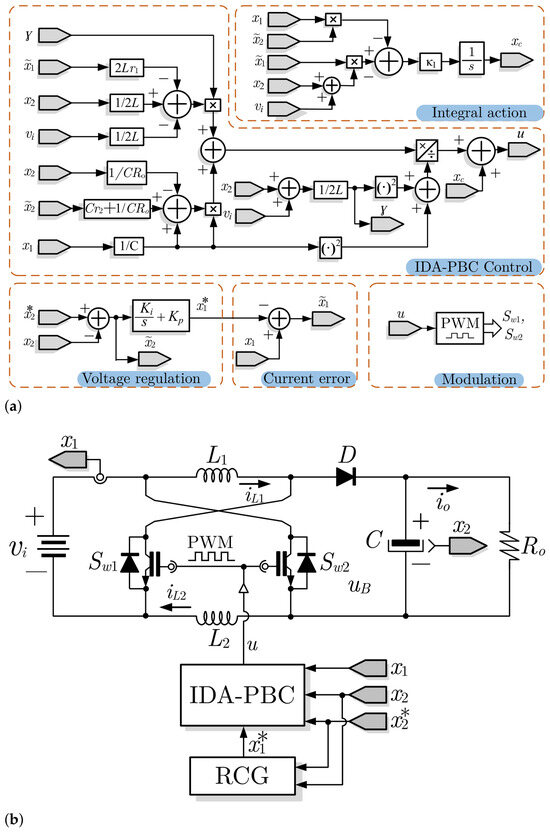
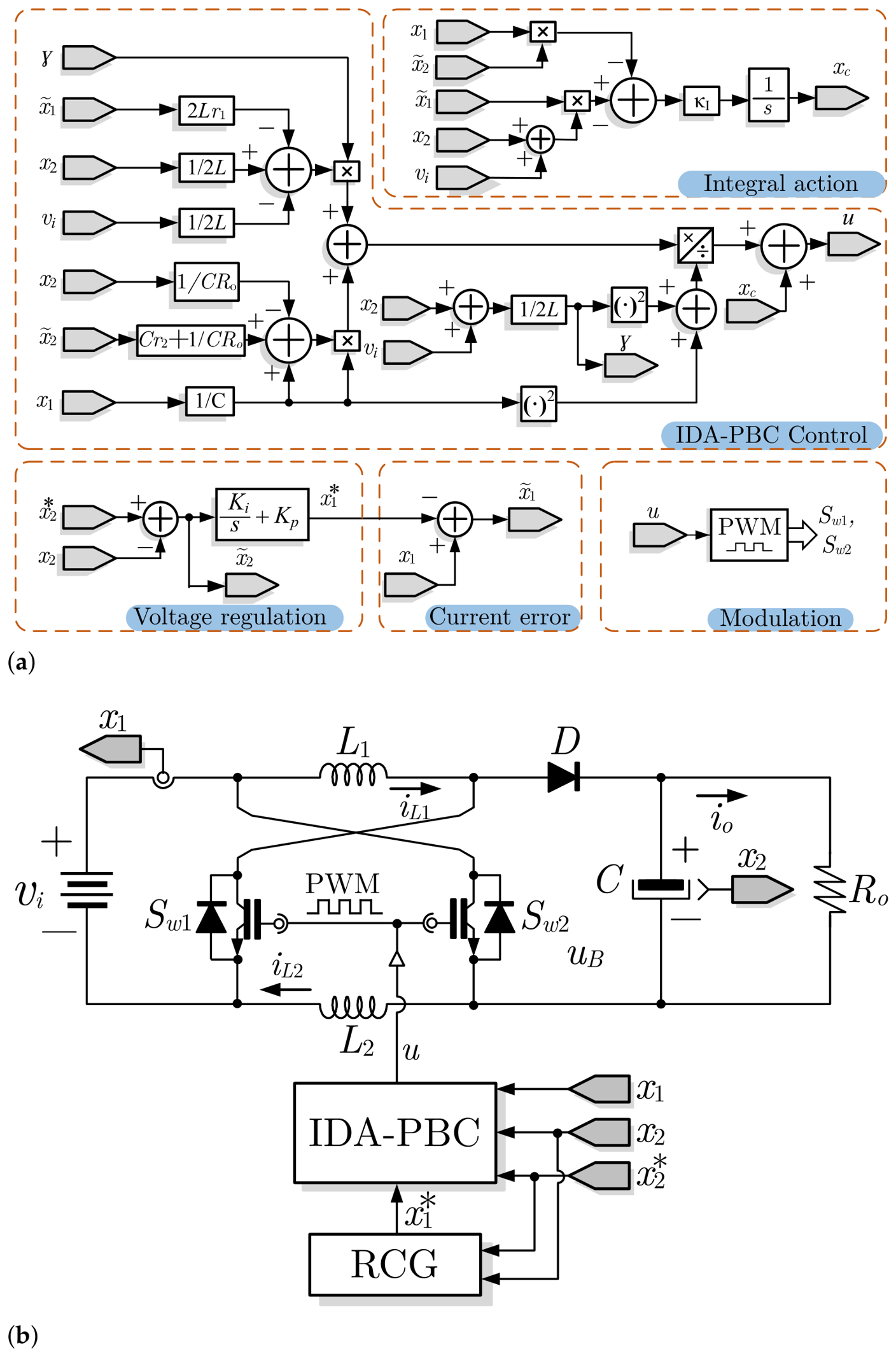
In this section, the CMC is designed based on the IDA-PBC theory for current tracking purposes. The resulting IDA-PBC scheme with dynamic extension is summarized in the following proposition and illustrated with the block diagram in Figure 2b.
Figure 2.
IDA-PBC control scheme: (a) detailed structure, (b) overall implementation.
Proposition 1.
Consider the ASL-BC system (Figure 1) verifying Assumptions 1–5, with bounded state x and control signal u, then the dynamic nonlinear controller
with the current reference computed by the RCG (21), a given voltage reference and the integral action in (19), with and sufficiently large tuning gains α, β and , is well-defined and asymptotically stabilizes the system trajectories towards the reference values.
Proof.
To fulfill the control objectives stated above, the following desired closed-loop dynamics are prescribed as
where (9) represents the desired port-Hamiltonian dynamics of the ASL-BC, in which and are the desired interconnection and damping matrices, respectively, and is the total energy function that serves as a Lyapunov function for the closed-loop system. The second Equation (10) defines the dynamics of the integral action , which is driven by the port characteristic matrix and the gradient , and is introduced to compensate for the steady-state error caused by the unmodeled parasitic resistances in the system. In particular, is the desired interconnection matrix and is the desired damping matrix, with both auxiliary matrices selected as
where the positive control gains and inject virtual damping into the system. Notice that setting , the desired interconnection matrix results in
Hence, interconnections are canceled, and the control scheme design is simplified. In addition, the total energy storage function is the sum of the desired Hamiltonian function and the dynamic extension energy function, and both are defined as
where
Notice that the control error is defined as the difference between the system state and the reference value, i.e.,
where is the current reference computed by the outer loop below in (21) and is the constant output voltage reference. Furthermore, the partial derivative of W with respect to the state x and the controller dynamic extension are
where is the dynamic extension (integral action) and is the integral gain. Recall that the dynamic extension is added to the control scheme to deal with non-modeled parasitic resistances in the system. Afterward, in order to compute the explicit controller u, the PCH system model (3) is matched with the desired closed-loop dynamics (9) as follows:
This matching equation equates the desired closed-loop dynamics with the open-loop ASL-BC model; its purpose is to bridge the physical plant description and the target stable closed-loop behavior, such that solving it for the control input u directly yields the IDA-PBC control. In this way, solving (16) for the control signal u results in
where is a pseudo inverse, and is obtained from [36]
Hence, based on (17), the control signal u results in (8), with and and the dynamic extension (integral action)
where . On the other hand, the stability of the current loop with the dynamic extension is proven straightforward. Consider the closed-loop desired energy function (12) as a Lyapunov function. Note that is a positive definite function and . In this way, the time derivative of (12) along the trajectories of (9) and (10) and considering the skew-symmetry property of , is computed as
where is negative definite an consequently the origin of (9) is stable in the sense of Lyapunov, and asymptotic stability is achieved by invoking La Salle’s invariance principle. □
Remark 3.
3.2. Reference Current Generator
The control law (8) requires both references and to implement the control error defined in (14) and to fulfill the control objectives (6) and (7). Meanwhile, the voltage error is obtained from the direct measurement of the output voltage and the explicit definition of the constant output voltage reference ; to implement the current error, besides the current measurement, a current reference needs to be defined. Different ways have been implemented in the literature for this end; for instance, the equilibrium point in (2) might act as the current reference if the load is known but it varies during operation and consequently an adaptation law to approximate the load is required if is used to construct [33,34]. On the other hand, based on traditional CMC, an outer voltage loop based on a simple PI action over the output voltage is traditionally proposed to generate the current reference ; for instance, see [12,15,35]. In this work, to avoid using adaptive schemes, and based on traditional CMC, an outer voltage loop based on a PI action over the output voltage is proposed to generate the current reference as
where and are the positive control gains to be selected. Remark that is used as input to the current loop in (14). In order to prove the stability of the outer loop, the time-scale separation principle is invoked, in accordance with the CMC framework [12,15,35]. It is considered that the current dynamics are faster than the voltage dynamics; therefore, it is possible to decouple these two dynamics. This decoupling is consistent with the singular perturbation theory provided in [37]. In this way, the inner loop ensures that ; consequently, the voltage dynamics in (1) are rewritten as
where denotes the steady-state value reached by the control signal u, and is now considered the new control input to dominate the output voltage dynamics. Recalling that ; then, Equation (22) can be rewritten in terms of the voltage error as
Afterwards, consider (23) in closed loop with (21), which result in
where . The equilibrium point of the last expression is and considering a new coordinate , the slow subsystem (24) can be expressed in the compact matrix form , as
where the stability of the equilibrium is determined by the eigenvalues of A. The characteristic polynomial of A is given by
By the Routh–Hurwitz stability criterion, both roots of (26) have strictly negative real parts if and only if and . Since , , , , and hold by construction, both conditions are satisfied for any admissible operating point. Therefore, the matrix A is Hurwitz, and the equilibrium of the slow subsystem is asymptotically stable, establishing the convergence The overall block diagram of the control scheme is presented in Figure 2.
4. Numerical and Experimental Results and Discussion
The proposed multi-loop nonlinear control strategy based on IDA-PBC given in (8)–(19) and (21), and shown in Figure 2b for the output voltage regulation of the ASL-BC is validated through both numerical and experimental results. In Table 1, the system parameters used for both cases are shown. To validate the performance, as well as the effectiveness of the proposed controller, the following real-life scenarios are considered for both numerical and experimental results:
Table 1.
System parameters.
i. Changes in the output load:The output resistance is varied between 100 and 126 , and a voltage reference equals to 120 V is set for the output voltage.
ii. Changes in the input voltage: Stepwise variations in the input voltage from 33 V to 43 V are implemented. The voltage reference is established at 120 V as well.
iii. Voltage reference changes: The voltage reference is configured to change in steps from 110 V to 120 V. In this case, the input voltage and the load are at their nominal constant values.
4.1. Simulation Results and Comparative Analysis
For simulation results, the ASL-BC is implemented using the SimPowerSystem toolbox from MATLAB/Simulink, version number R2025a. Consequently, for both inductors, the parasitic resistance is set to 0.5 . Additionally, for the three scenarios, the changes are introduced at a rate of 4 Hz. The comparative analysis considers the proposed IDA-PBC controller with the dynamic extension, a nested PI controller that substitutes the proposed inner current loop by a standard PI action over the current error , and finally the PI-PI controller designed in [13]. The gains for each controller are gathered in Table 2. In addition, Table 3 presents the performance error indices computed for the output voltage error of each controller under the three operating scenarios. Four indices are considered: the Integral of Squared Error (ISE), the Integral of Absolute Error (IAE), the Integral of Time-Weighted Absolute Error (ITAE), and the Integral of Time-Weighted Squared Error (ITSE). Overall, the proposed IDA-PBC controller achieves the smallest error values across all scenarios, confirming the superior tracking performance observed in Figure 3, Figure 4 and Figure 5.
Table 2.
Numerical test control gains for each controller.
Table 3.
Performance error indices for the comparative analysis of the three controllers under three operating scenarios. The smallest error value in each category is highlighted in bold.
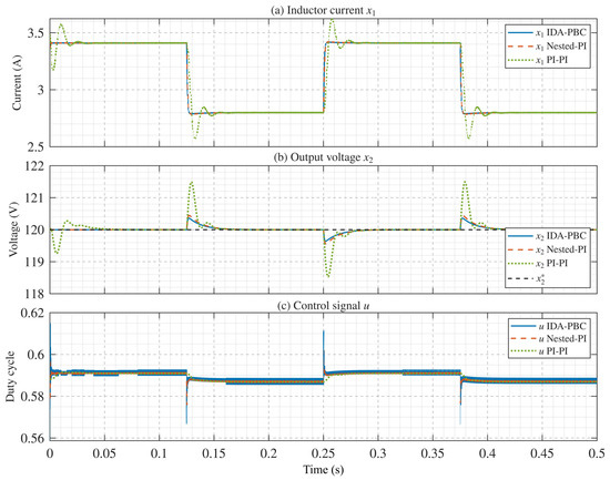
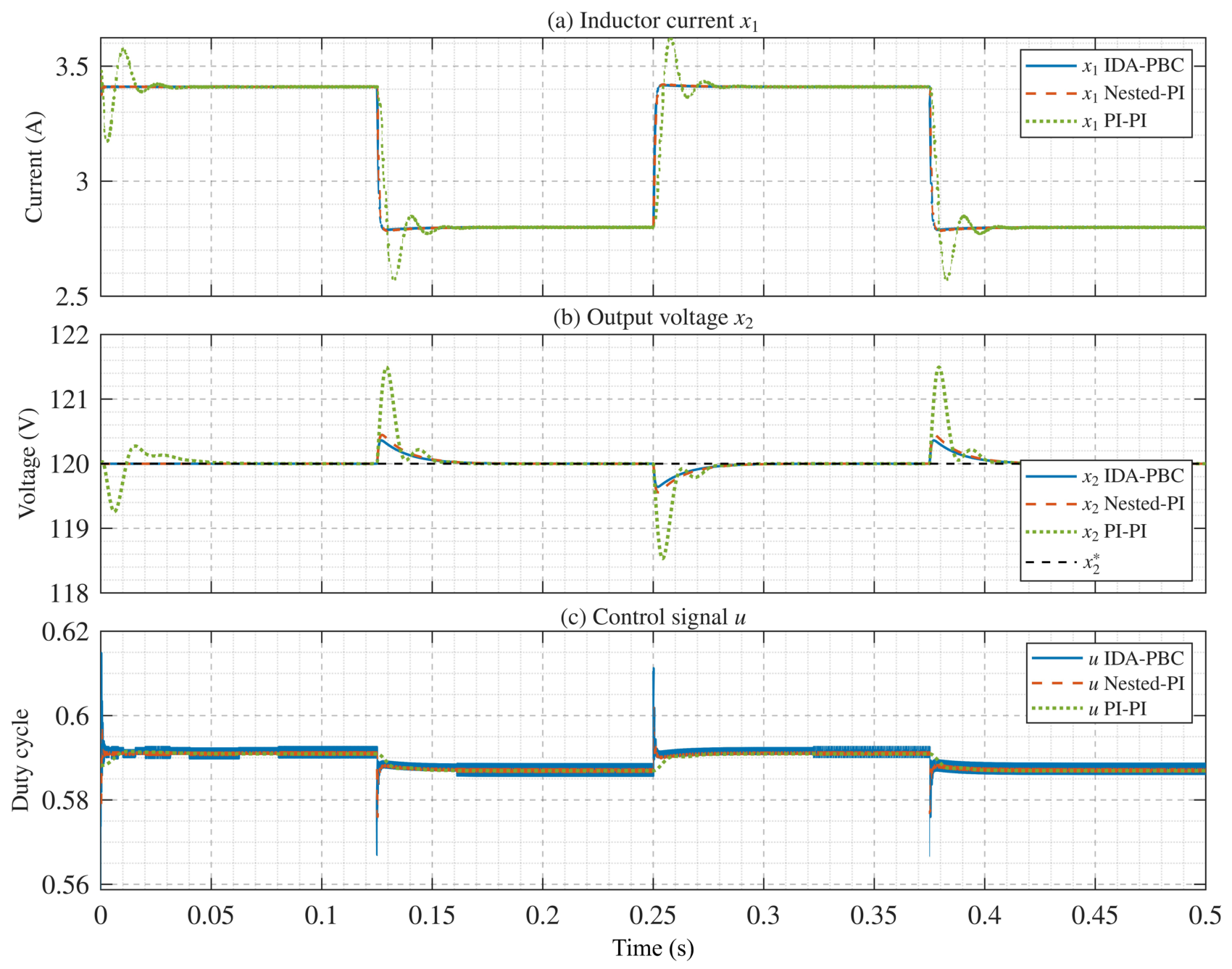
Figure 3.
Simulation comparison of the proposed IDA-PBC controller against the Nested-PI and the controller in [13] for load step change scenario.
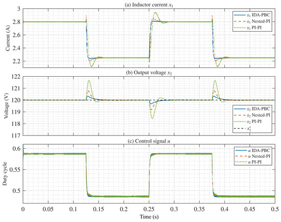
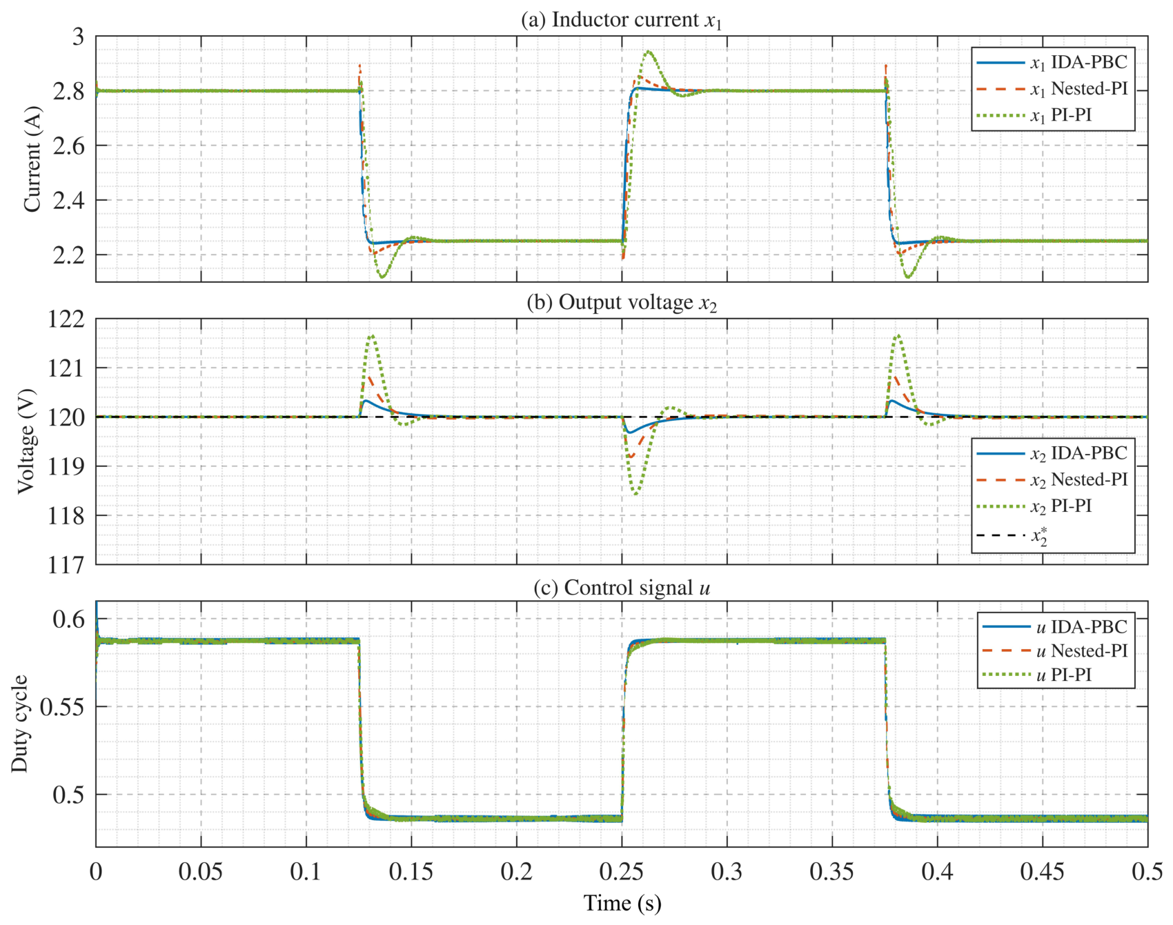
Figure 4.
Simulation comparison of the proposed IDA-PBC controller against the Nested-PI and the controller in [13] for input voltage variation scenario.
Figure 5.
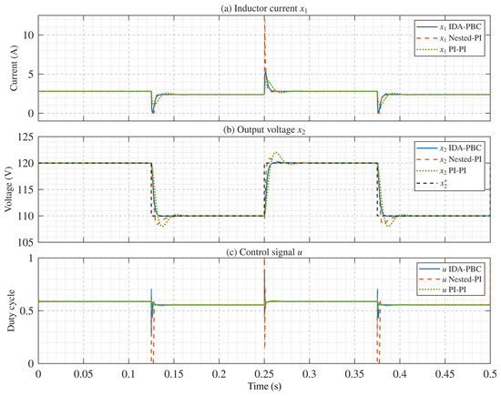
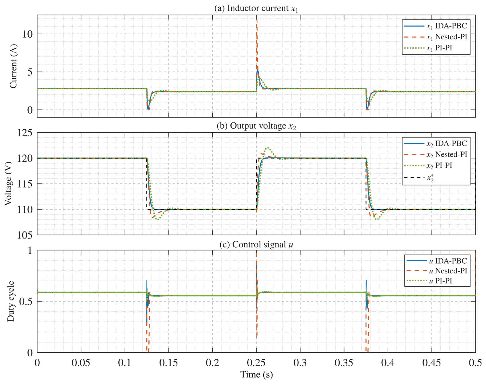
Simulation comparison of the proposed IDA-PBC controller against the Nested-PI and the controller in [13] for output voltage reference transition scenario.
4.2. Numerical Results: Changes in the Output Load
The performance of the three controllers under load variations is depicted in Figure 3. First, Figure 3a shows the inductor current for each controller, which varies from an initial condition of A to A at each load transition. Notice that the IDA-PBC and Nested-PI responses are close to each other, whereas the PI-PI controller [13] exhibits an oscillatory behavior, reaching A at each transition. The output voltage performance for the three controllers is shown in Figure 3b. In this case, all controllers achieve a similar settling time of approximately s; however, the proposed IDA-PBC presents smaller over- and undershoots with respect to the other controllers, with a deviation of V. Finally, the control signal u is shown in Figure 3c, where it is observed that the IDA-PBC controller exhibits a more energetic response than the others, with larger transient over- and undershoots that remain within feasible operating bounds.
4.3. Numerical Results: Changes in the Input Voltage
The performance of the three controllers under input voltage variations is depicted in Figure 4. First, Figure 4a shows the inductor current for each controller, which varies from A to A at each input voltage transition. Notice that the IDA-PBC response is less oscillatory and more stepwise than the other two controllers, which display a more oscillatory behavior. The output voltage performance for the all controllers is shown in Figure 4b. In this case, the IDA-PBC and Nested-PI controllers reach the reference in approximately s, while the PI-PI controller [13] takes approximately s with a more oscillatory response. The proposed IDA-PBC presents smaller over- and undershoots with respect to the other controllers, with a deviation of V. Finally, the control signal u is shown in Figure 4c, where the three controllers remain within feasible operating bounds, experiencing duty cycle variations from to with smooth transitions.
4.4. Numerical Results: Reference Voltage Changes
The performance of the three controllers under output voltage reference variations is depicted in Figure 5. First, Figure 5a shows the inductor current for each controller, which varies from A to A at each transition. Notice that the IDA-PBC and Nested-PI controllers reach steady state in approximately s, while the PI-PI controller [13] takes approximately s with a more oscillatory response, yet with smaller over- and undershoots than the former. The output voltage performance for the three controllers is shown in Figure 5b. In this case, the IDA-PBC controller reaches the reference in approximately s, while the Nested-PI and PI-PI [13] controllers take approximately s and s, respectively, exhibiting a more oscillatory response. The proposed IDA-PBC presents no over- or undershoots in contrast to the other controllers. Finally, the control signal u is shown in Figure 5c, where the IDA-PBC and PI-PI [13] controllers remain within feasible operating bounds, while the Nested-PI exhibits a large transient excursion of the control signal, reaching near-zero values and approaching saturation at unity. All control signals present duty cycle variations from to .
4.5. Experimental Results and Dynamic Extension Comparative Analysis
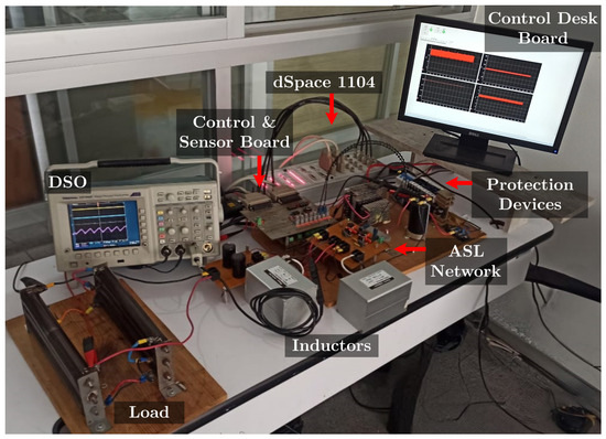
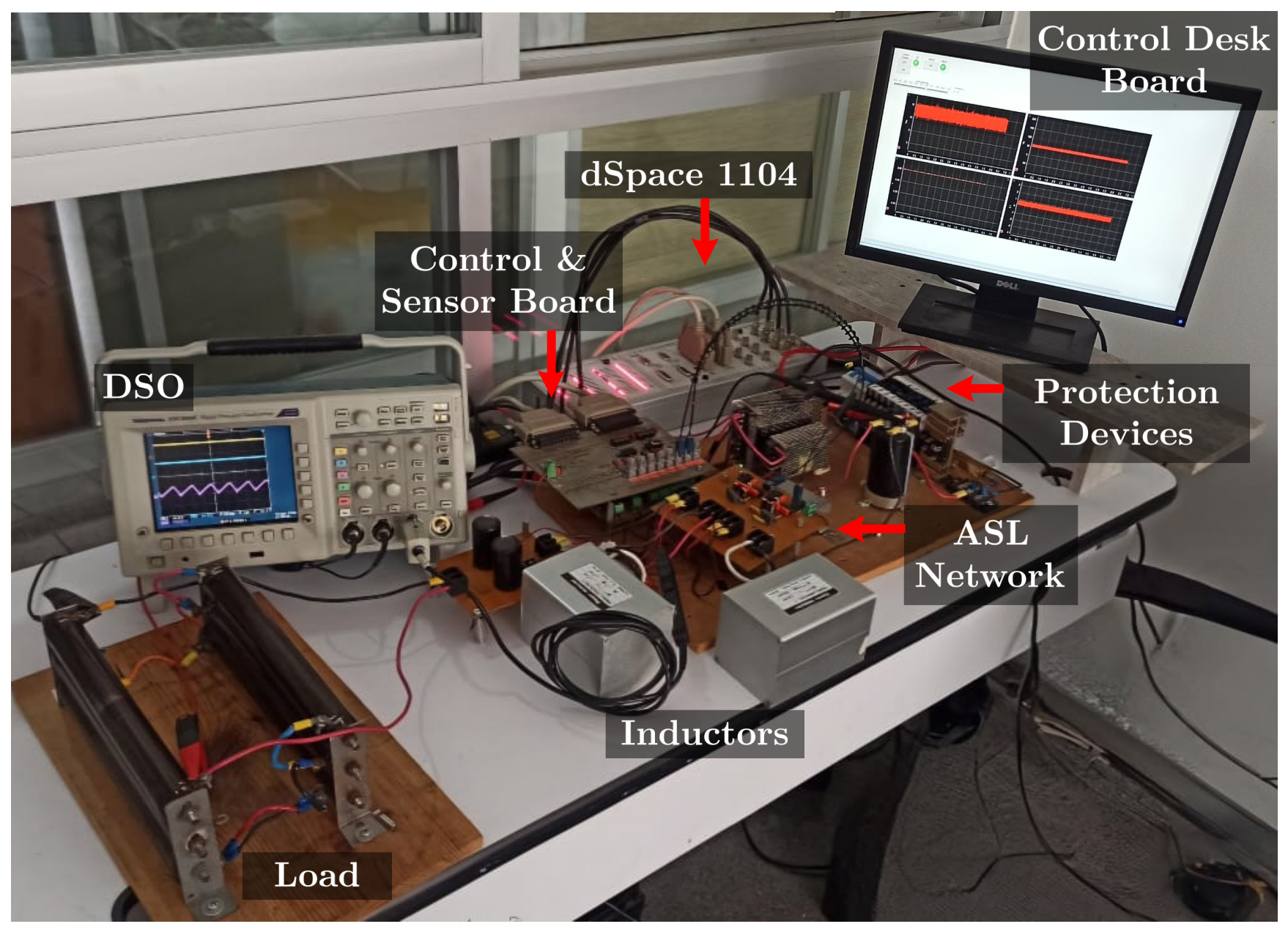
In Table 1, the control parameters are shown for the experimental case. The experimental test bench depicted in Figure 6 is built, where a dSPACE 1104 control board is used for the digital implementation of the control scheme. Furthermore, in each aforementioned scenario, the obtained results are shown with and without the dynamic extension to emphasize the importance of non-modeled parasitic resistance effect mitigation and steady-state error elimination. Note that changes are at a rate of Hz. The controller gains are listed in Table 4.
Figure 6.
Experimental test bench of the ASL-BC.
Table 4.
Experimental control gains for the proposed controller.
4.6. Experimental Results: Changes in the Output Load
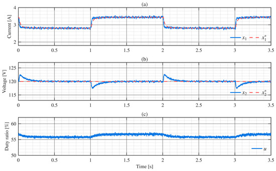
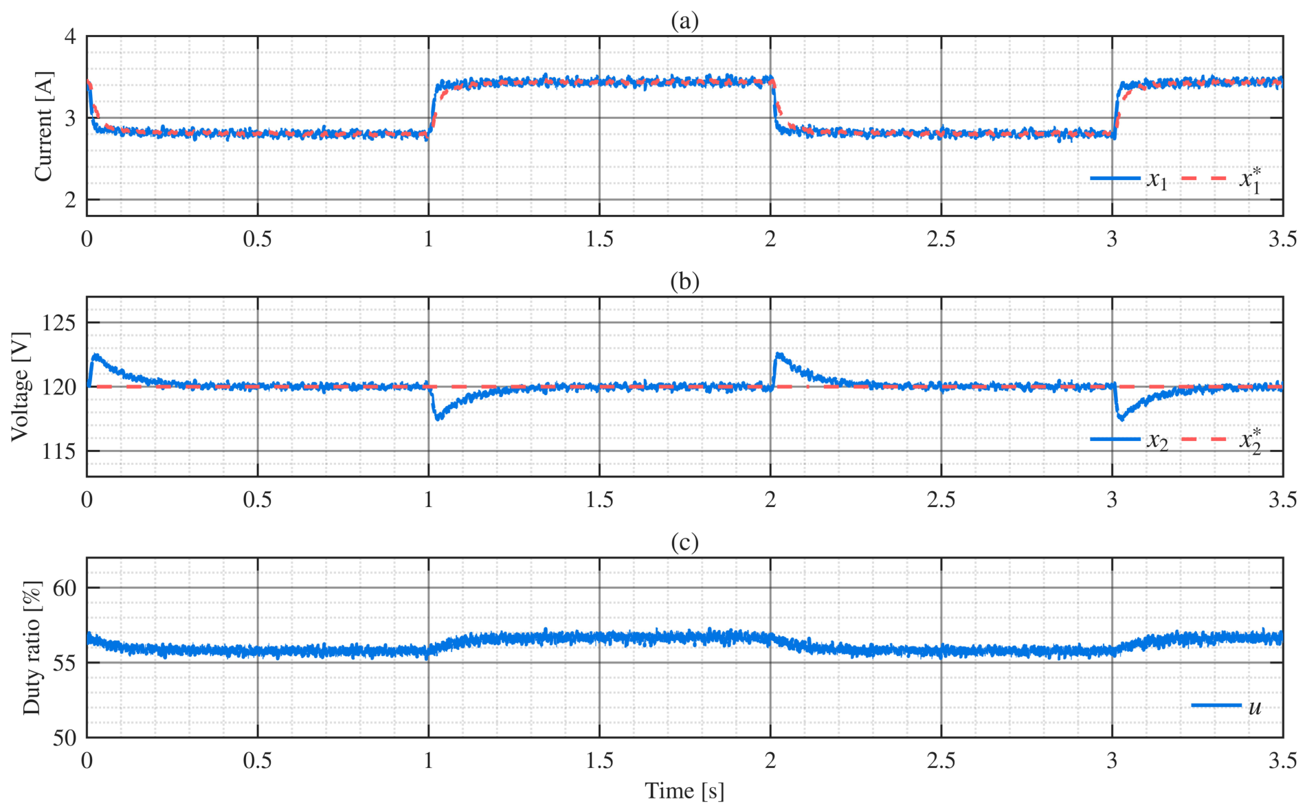
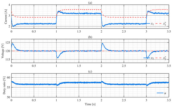
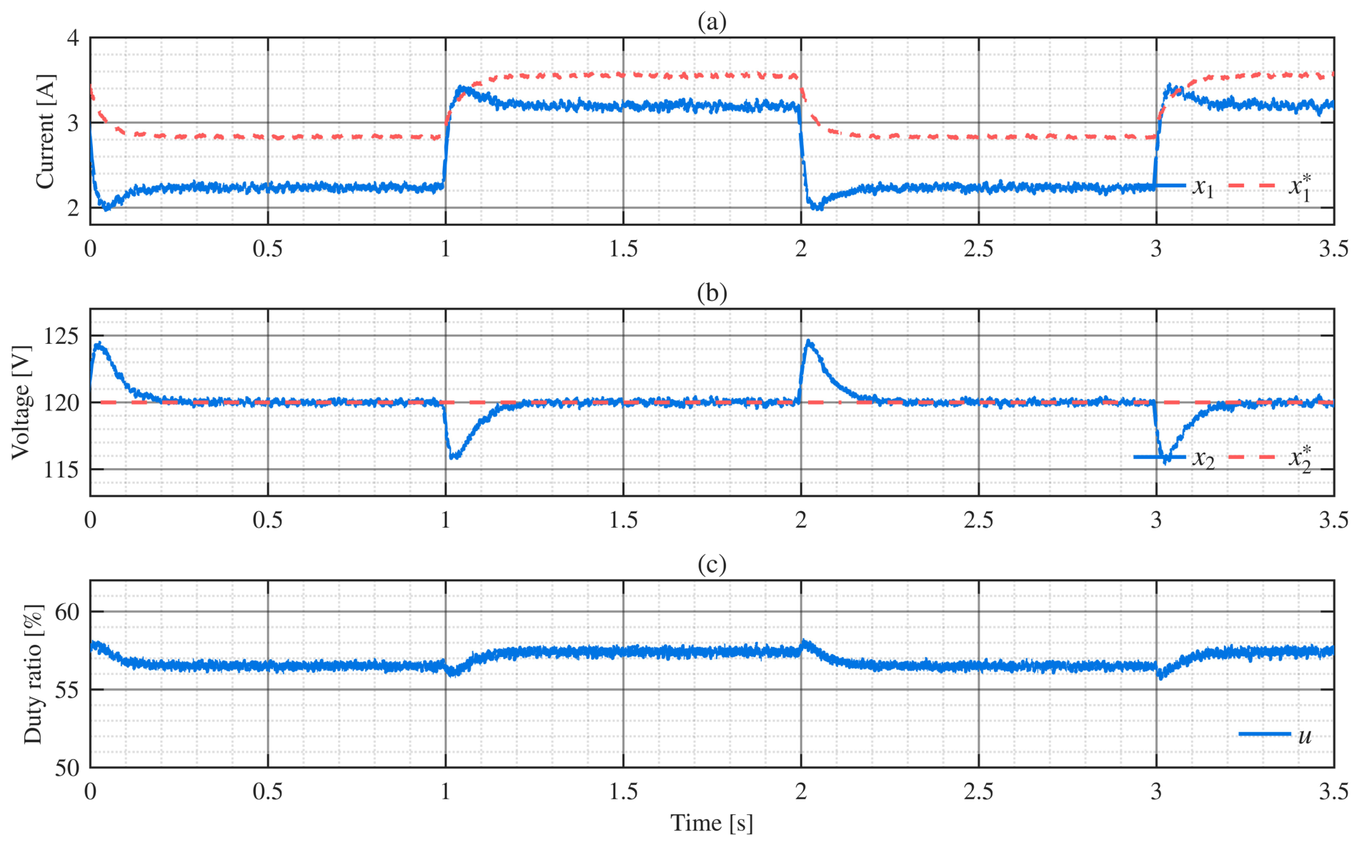
In Figure 7, the behavior of the system states and the control signal following step changes in the output resistance is shown. To begin with, Figure 7a depicts the tracking of the current to the desired value . It shows tight tracking with no steady-state error within a range of 2.8 A and 3.44 A. In addition, the regulation of the output voltage at 120 V is depicted in Figure 7b. The voltage over- and undershoots are due to stepwise variations in the output load. However, these voltage transients are approximately of 120 V with a settling time to reference value of s. Remark that load variation causes output power variations between 144 W (100 ) and W (126 ). Thus, Figure 7a,b reflect the fulfillment of the control objectives mentioned in Section 3. The time history of u is displayed in Figure 7c, where variations are from 55.83% to 56.71%. On the other hand, the behavior of the control scheme without the integral action (19) is shown in Figure 8. The tracking lack of to is evident in Figure 8a, where a steady-state error is present. Additionally, the error magnitude decreases if the control gain increases; however, increasing the value of causes undesirable noise in the transient response of the current . The regulation of voltage to the desired voltage at 120 V is illustrated in Figure 8b. The magnitude of the voltage peaks caused by variations in the output load is higher compared to Figure 7b. Simultaneously, the control signal shown in Figure 8c differs from the values of its counterpart in Figure 7c. Notice that the controller performance without the dynamic extension does not achieve the current tracking objective. However, voltage regulation is assured and stability is exhibited.
Figure 7.
Experimental results for the case of changes in output load with controller dynamic extension. (a) Inductor current and reference current , (b) output voltage and reference voltage , (c) control signal u.
Figure 8.
Experimental results for changes in output load without controller dynamic extension. (a) Inductor current and reference current , (b) output voltage and reference voltage , (c) control signal u.
4.7. Experimental Results: Changes in the Input Voltage
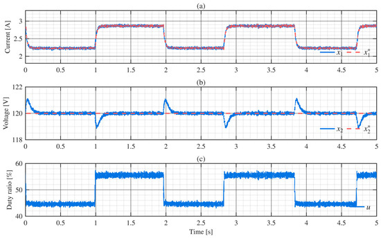
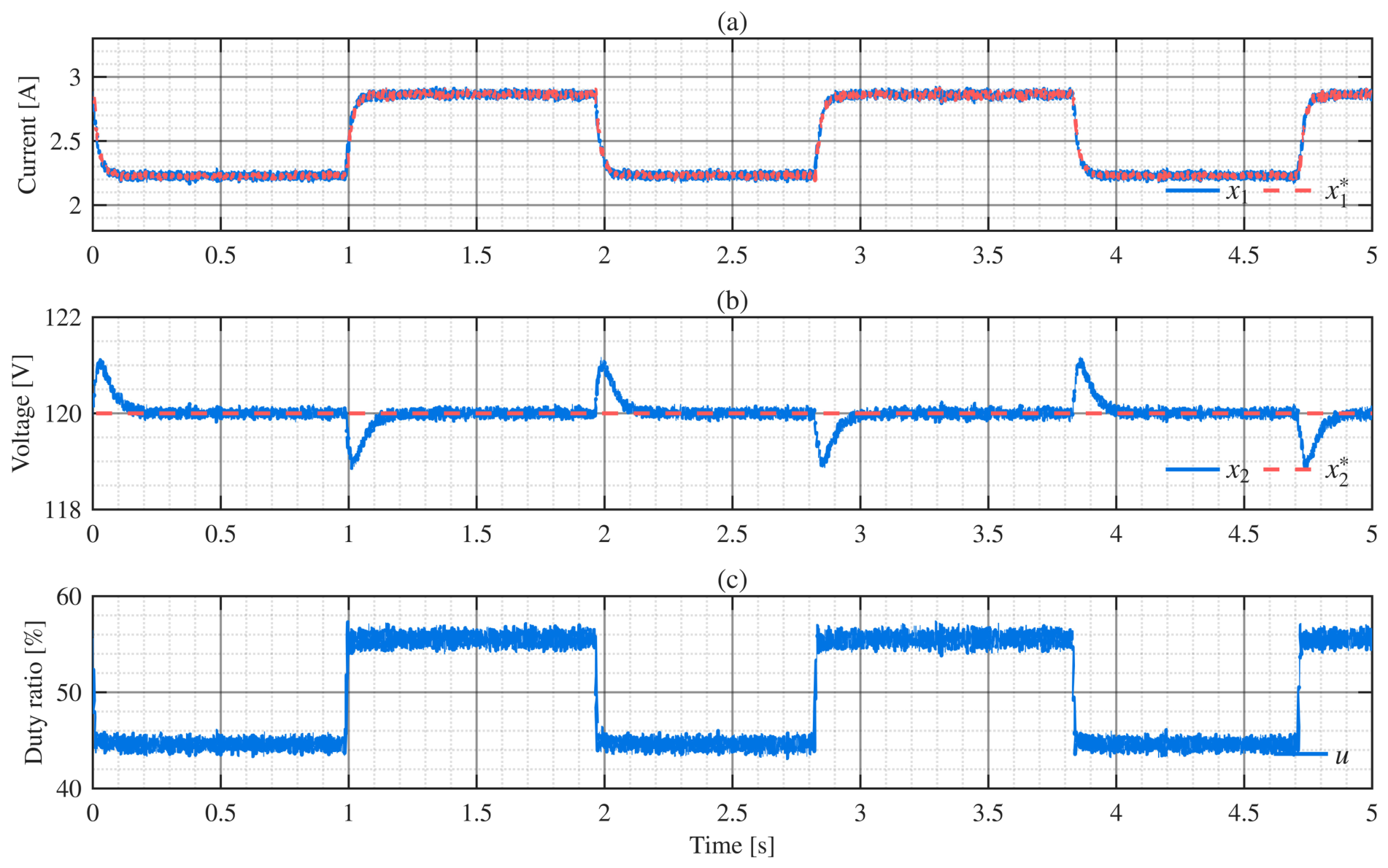
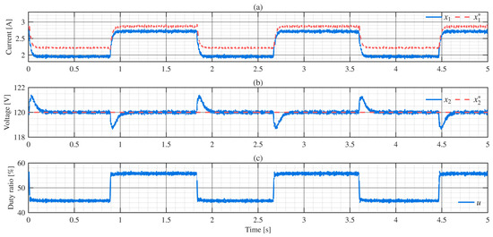
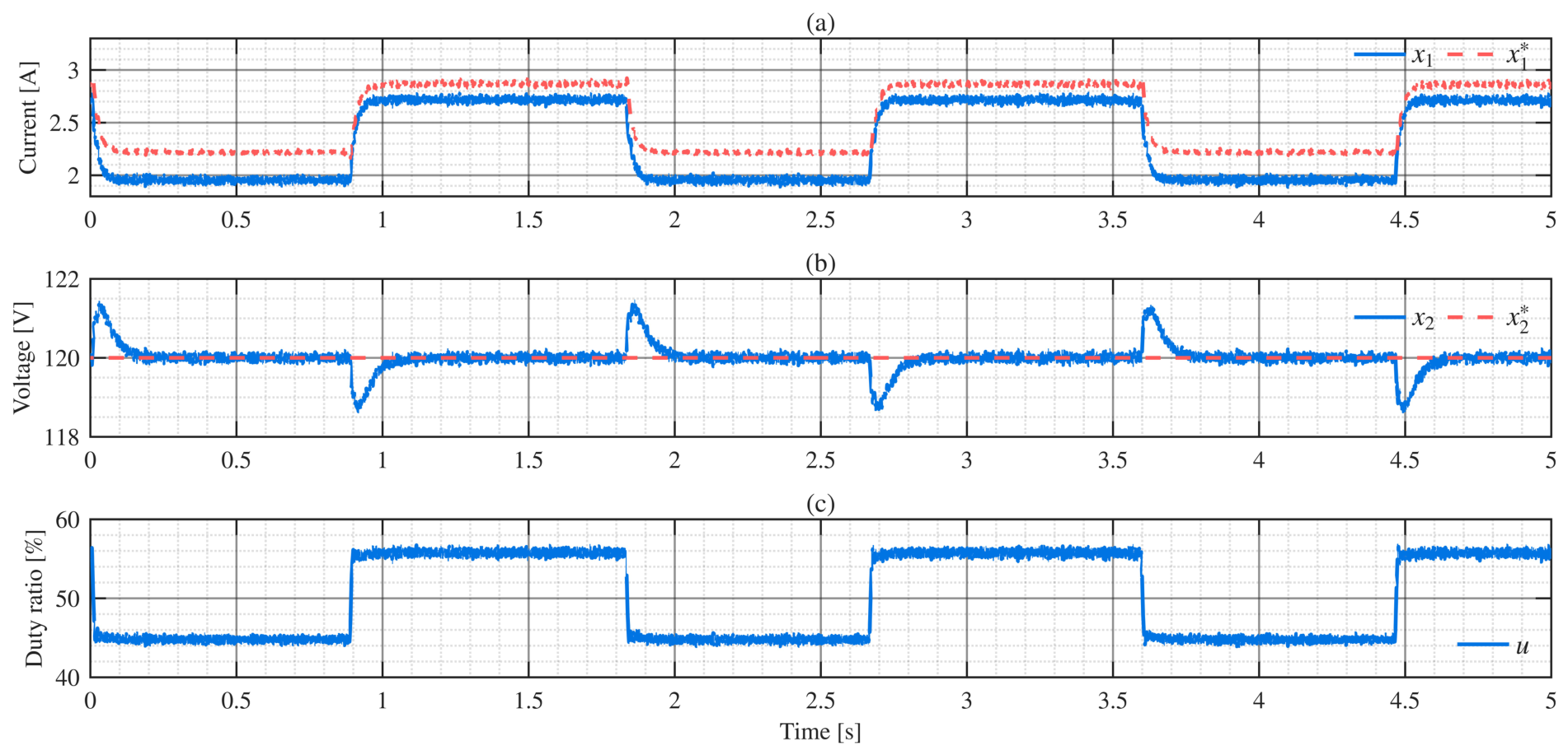
The performance of the control scheme following changes in input voltage is illustrated in Figure 9. In addition, in Figure 9a, a tight current tracking to is shown with variations from 2.22 A to 2.85 A, and no steady-state error is exhibited. Moreover, Figure 9b shows the output voltage regulation to the reference value of 120 V, where transients of approximately V. are exhibited. In addition, the settling time to the reference value is s. Furthermore, the control signal is observed in Figure 9c, and displays adjustments from 44.8% to 55.6% to achieve the current tracking and voltage regulation. On the other hand, Figure 10 shows the closed-loop performance when the integral action (19) is not considered. The steady-state error of current is shown in Figure 10a, where the maximum error is almost 0.3 A. It is possible to reduce the difference between current and its reference value by increasing the control gains. However, it causes voltage and current overshoots that can result in component damage. Notice that although the current tracking target is not reached, the voltage regulation to the desired reference is achieved in Figure 10b. Similarly, the control signal in Figure 10c, adjusts itself to cope with the stepwise variations in the input voltage.
Figure 9.
Experimental results for step changes in the input voltage with controller dynamic extension. (a) Inductor current and reference current , (b) output voltage and reference voltage , (c) control signal u.
Figure 10.
Experimental results for step changes in the input voltage without controller dynamic extension. (a) Inductor current and reference current , (b) output voltage and reference voltage , (c) control signal u.
4.8. Experimental Results: Reference Voltage Changes
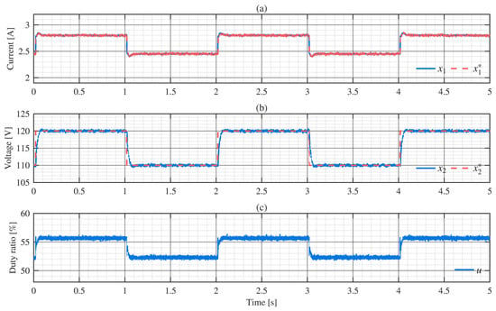
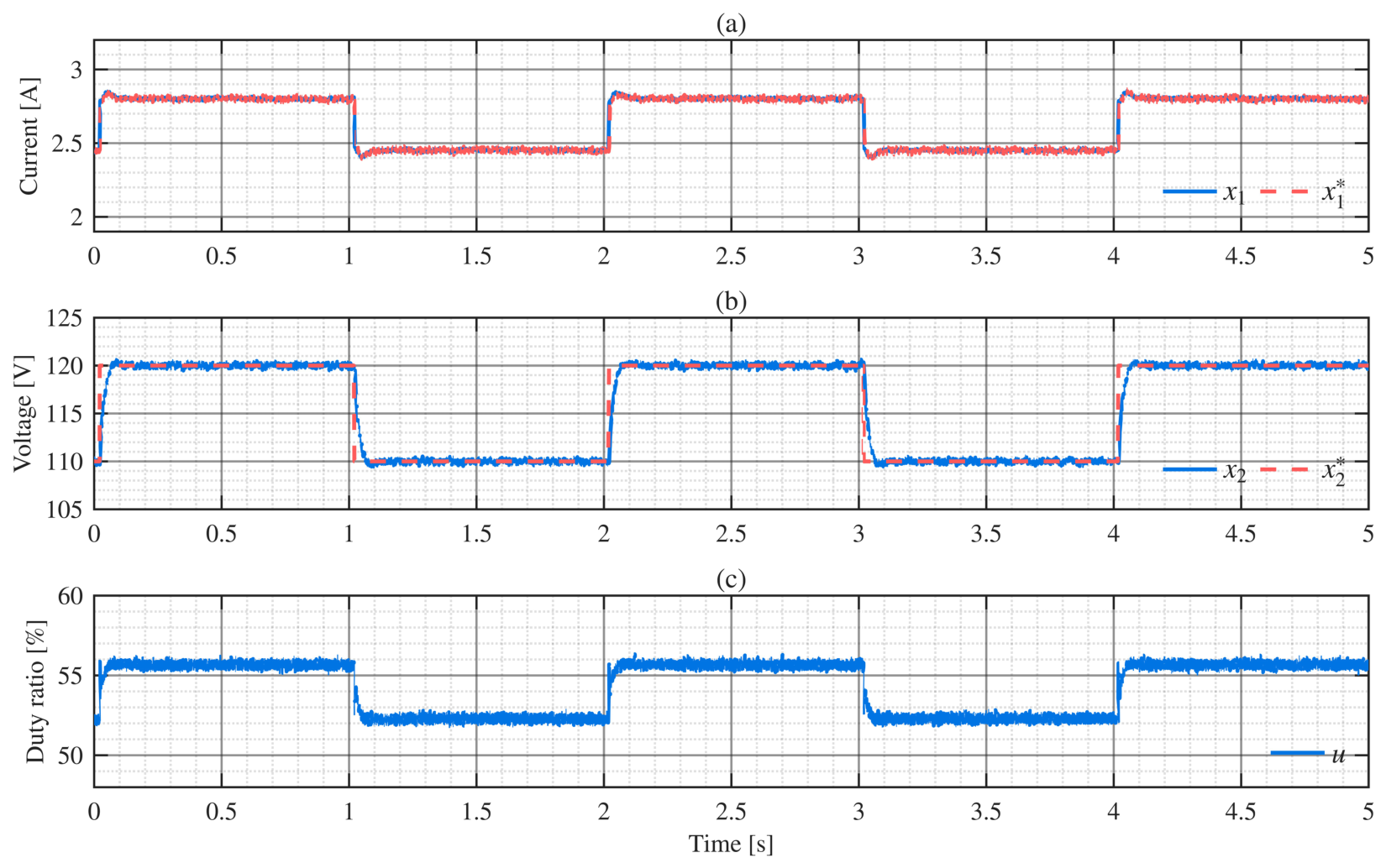
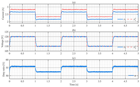
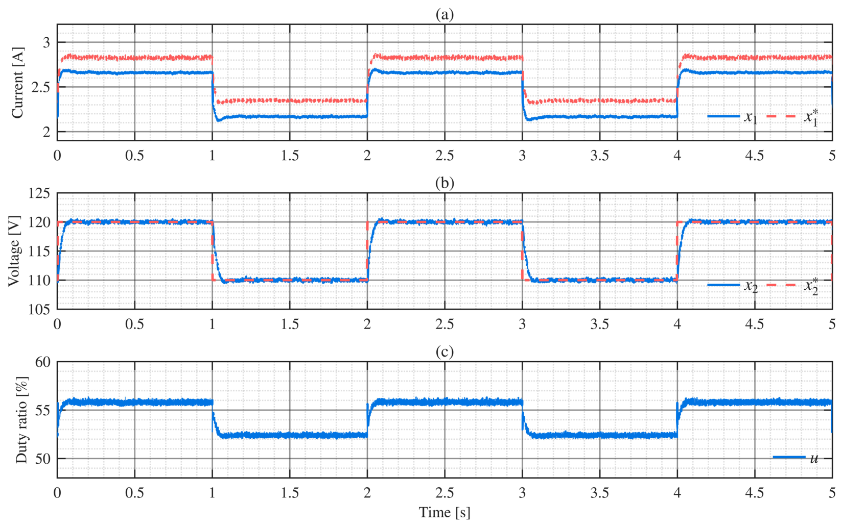
Closed-loop experimental results considering changes in the output voltage reference are shown in Figure 11. Again, the variations are performed in steps at a rate of Hz from 110 V to 120 V. The output load is set at , and the resulting output power ranges from W () to W (). In Figure 11a, tight current tracking is shown with no steady-state error. Afterward, tight voltage regulation is depicted in Figure 11b despite sudden variations in . Hence, the control objectives are achieved. In addition, the control signal in Figure 11c displays changes between ( V) and ( V). In comparison, in Figure 12, the closed-loop system behavior without dynamic extension is observed for this case scenario. Figure 12a shows the steady-state error of the current, which is almost 0.2 A. Nevertheless, the voltage regulation illustrated in Figure 12b is preserved. Finally, the control signal is observed in Figure 12c, which presents changes between and .
Figure 11.
Experimental results for step changes in the voltage reference with controller dynamic extension. (a) Inductor current and reference current , (b) output voltage and reference voltage , (c) control signal u.
Figure 12.
Experimental results for step changes in the voltage reference without controller dynamic extension. (a) Inductor current and reference current , (b) output voltage and reference voltage , (c) control signal u.
5. Conclusions and Future Work
This paper has presented the control strategy design for current tracking and voltage regulation in an ASL-BC. The proposed approach combined interconnection and damping assignment PBC with dynamic extension. The control strategy achieved high-performance tracking of the desired current and output voltage regulation, and no restrictions were imposed over the tuning gains nor singularities were present in the control law. Furthermore, this scheme ensured the asymptotic stability and passivity of the closed-loop system, whereas the dynamic extension improved tracking and regulation performance by eliminating the effect of the non-modeled parasitic resistances present in the system. Numerical and experimental results have shown fast and accurate tracking of the desired current and regulation of the output voltage, even in the presence of load changes, input voltage disturbances, and output voltage reference changes. For future work, the proposed control strategy can be extended to other step-up or step-down high-gain DC-DC converters to exploit renewable energy sources like FC or PV systems.
Author Contributions
D.L.-C., P.R.M.-R., D.R.-C., R.C., A.H.-G. and J.A.V.-L. contributed to the development of the overall document writing and research, modeling, controller design and experimental results. All authors have read and agreed to the published version of the manuscript.
Funding
This research received no external funding.
Institutional Review Board Statement
Not applicable.
Informed Consent Statement
Not applicable.
Data Availability Statement
The original contributions presented in this study are included in the article. Further inquiries can be directed to the corresponding authors.
Conflicts of Interest
The authors declare no conflicts of interest.
Abbreviations
The following abbreviations are used in this manuscript:
| IDA-PBC | Interconnection and damping assignment passivity-based control |
| DC | Direct current |
| BC | Boost converter |
| PV | Photovoltaic |
| FC | Fuel cell |
| ASL | Active switched inductor |
| CMC | Current-mode control |
| PI | Proportional–integral |
| EL | Euler–Lagrange |
| RCG | Reference current generator |
| PCH | Port-controlled Hamiltonian system |
| CCM | Continuous conduction mode |
| DCM | Discontinuous conduction mode |
| Input voltage | |
| Converter inductors | |
| Active switches | |
| D | Diode |
| C | Capacitor |
| Nominal resistive load | |
| , | Inductor current |
| , | Output capacitor voltage |
| u | Duty cycle, control signal |
| Nominal duty cycle | |
| Inductor current eq. point | |
| Output capacitor voltage eq. point | |
| (Desired) Interconnection matrix | |
| (Desired) Dissipation matrix | |
| (Desired) Hamiltonian function | |
| Port characteristic matrix | |
| Disturbance vector | |
| Current reference | |
| Voltage reference | |
| , | Control gains |
| Integral action | |
| Integral gain | |
| Error variable | |
| W | Energy function |
References
- Tang, Z.; Yang, Y.; Blaabjerg, F. Power electronics: The enabling technology for renewable energy integration. CSEE J. Power Energy Syst. 2022, 8, 39–52. [Google Scholar] [CrossRef] [Scilit]
- Jalilzadeh, T.; Rostami, N.; Babaei, E.; Maalandish, M. Nonisolated Topology for High Step-Up DC–DC Converters. IEEE J. Emerg. Sel. Top. Power Electron. 2023, 11, 1154–1168. [Google Scholar] [CrossRef] [Scilit]
- Forouzesh, M.; Siwakoti, Y.P.; Gorji, S.A.; Blaabjerg, F.; Lehman, B. Step-Up DC–DC Converters: A Comprehensive Review of Voltage-Boosting Techniques, Topologies, and Applications. IEEE Trans. Power Electron. 2017, 32, 9143–9178. [Google Scholar] [CrossRef] [Scilit]
- Ammar, A.M.; Spliid, F.M.; Nour, Y.; Knott, A. A 1-MHz Resonant LED Driver with Charge-Pump-Based Power Factor Correction. IEEE J. Emerg. Sel. Top. Power Electron. 2021, 9, 5838–5850. [Google Scholar] [CrossRef] [Scilit]
- Yang, L.S.; Liang, T.J.; Chen, J.F. Transformerless DC–DC converters with high step-up voltage gain. IEEE Trans. Ind. Electron. 2009, 56, 3144–3152. [Google Scholar] [CrossRef] [Scilit]
- Mirzaee, A.; Moghani, J.S. Coupled Inductor-Based High Voltage Gain DC–DC Converter For Renewable Energy Applications. IEEE Trans. Power Electron. 2020, 35, 7045–7057. [Google Scholar] [CrossRef]
- Rajabi, A.; Rajaei, A.; Tehrani, V.M.; Dehghanian, P.; Guerrero, J.M.; Khan, B. A Non-Isolated High Step-Up DC-DC Converter Using Voltage Lift Technique: Analysis, Design, and Implementation. IEEE Access 2022, 10, 6338–6347. [Google Scholar] [CrossRef] [Scilit]
- Fard, H.J.; Sadeghzadeh, S.M. A three-winding coupled-inductor nonisolated high step-up interleaved DC–DC converter with low switch stress. Electr. Eng. 2022, 104, 4335–4346. [Google Scholar] [CrossRef] [Scilit]
- Gu, Y.; Chen, Y.; Zhang, B.; Qiu, D.; Xie, F. High Step-Up DC–DC Converter with Active Switched LC-Network for Photovoltaic Systems. IEEE Trans. Energy Convers. 2019, 34, 321–329. [Google Scholar] [CrossRef] [Scilit]
- Tang, Y.; Tong, H.; Afzal, R.; Guo, Y. High step-up ZVT Converter Based on Active switched Coupled inductors. IEEE Access 2020, 13, 15178–15187. [Google Scholar] [CrossRef] [Scilit]
- Samiullah, M.; Iqbal, A.; Ashraf, I.; Maroti, P.K. Voltage Lift Switched Inductor Double Leg Converter with Extended Duty Ratio for DC Microgrid Application. IEEE Access 2021, 9, 85310–85325. [Google Scholar] [CrossRef] [Scilit]
- Diaz-Saldierna, L.; Leyva-Ramos, J.; Langarica-Cordoba, D.; Ortiz-Lopez, M. Energy processing from fuel-cell systems using a high-gain power dc-dc converter: Analysis, design, and implementation. Int. J. Hydrogen Energy 2021, 46, 25264–25276. [Google Scholar] [CrossRef] [Scilit]
- Reyes-Cruz, D.; Martinez-Rodriguez, P.; Langarica-Cordoba, D.; Vazquez-Guzman, G.; Sosa-Zuñiga, J.; Ramirez-Rivera, V. Control strategies and experimental validation for high-gain non-isolated double inductor boost converter. Eng. Sci. Technol. Int. J. 2023, 37, 101294. [Google Scholar] [CrossRef] [Scilit]
- Langarica-Cordoba, D.; Martinez-Rodriguez, P.R.; Diaz-Saldierna, L.H.; Leyva-Ramos, J.; Reyes-Cruz, D.; Iturriaga-Medina, S. Passivity-based control for a DC/DC high-gain transformerless boost converter. Asian J. Control 2023, 25, 26–39. [Google Scholar] [CrossRef] [Scilit]
- Beltrán, C.A.; Diaz-Saldierna, L.H.; Langarica-Cordoba, D.; Martinez-Rodriguez, P.R. Passivity-Based Control for Output Voltage Regulation in a Fuel Cell/Boost Converter System. Micromachines 2023, 14, 187. [Google Scholar] [CrossRef] [Scilit] [PubMed]
- Lei, B.; Zhang, T.; Fei, S. An improved nonlinear robust control design for grid-side converter of VSC-HVDC connected to wind power generation system. Electr. Eng. 2018, 100, 2309–2318. [Google Scholar] [CrossRef] [Scilit]
- Gao, C.; Tan, F. A new PBC control method using JSOA technique and KF-estimation in an LTCL-filtered grid-tied inverter system. Electr. Eng. 2025, 107, 13169–13183. [Google Scholar] [CrossRef] [Scilit]
- Abdolahi, M.; Adabi, J.; Mousavi, S.Y.M. Implementation and control of a buck–boost converter connected to a constant power load in a DC microgrid. Electr. Eng. 2025, 107, 1483–1492. [Google Scholar] [CrossRef] [Scilit]
- Zhu, Y.; Zhang, Y.; Xia, L. The control for a five-level grid-connected inverter based on passive sliding mode. Electr. Eng. 2025, 107, 5123–5135. [Google Scholar] [CrossRef] [Scilit]
- Ortega, R.; Perez, J.A.L.; Nicklasson, P.J.; Sira-Ramirez, H.J. Passivity-Based Control of Euler-Lagrange Systems: Mechanical, Electrical and Electromechanical Applications; Springer: London, UK, 1998. [Google Scholar]
- Ortega, R.; van der Schaft, A.; Maschke, B.; Escobar, G. Interconnection and damping assignment passivity-based control of port-controlled Hamiltonian systems. Automatica 2002, 38, 585–596. [Google Scholar] [CrossRef] [Scilit]
- Ortega, R.; Romero, J.G.; Borja, P.; Donaire, A. PID Passivity-Based Control of Nonlinear Systems with Applications; Wiley: Hoboken, NJ, USA; IEEE Press: New York, NY, USA, 2021. [Google Scholar]
- Cupelli, M.; Gurumurthy, S.K.; Bhanderi, S.K.; Yang, Z.; Joebges, P.; Monti, A.; De Doncker, R.W. Port controlled Hamiltonian modeling and IDA-PBC control of dual active bridge converters for DC microgrids. IEEE Trans. Ind. Electron. 2019, 66, 9065–9075. [Google Scholar] [CrossRef] [Scilit]
- Jeung, Y.C.; Lee, D.C.; Dragičević, T.; Blaabjerg, F. Design of passivity-based damping controller for suppressing power oscillations in DC microgrids. IEEE Trans. Power Electron. 2020, 36, 4016–4028. [Google Scholar] [CrossRef] [Scilit]
- Gandarilla, I.; Santibañez, V.; Sandoval, J. Control of a self-balancing robot with two degrees of freedom via IDA-PBC. ISA Trans. 2019, 88, 102–112. [Google Scholar] [CrossRef] [Scilit]
- Arpenti, P.; Ruggiero, F.; Lippiello, V. A constructive methodology for the IDA-PBC of underactuated 2-dof mechanical systems with explicit solution of PDEs. Int. J. Control Autom. Syst. 2022, 20, 283–297. [Google Scholar] [CrossRef] [Scilit]
- Franco, E. IDA-PBC with adaptive friction compensation for underactuated mechanical systems. Int. J. Control 2021, 94, 860–870. [Google Scholar] [CrossRef] [Scilit]
- Harandi, M.R.J.; Namvar, M.; Taghirad, H.D. Stabilization of Robots with Actuator Constraints via Interconnection and Damping Assignment. IEEE Trans. Control Syst. Technol. 2023, 31, 2945–2952. [Google Scholar] [CrossRef] [Scilit]
- Fan, B.; Hu, Q.; Wang, J.; Zhao, Y.; Zhou, H.; Sun, L. Active disturbance observation rejection control based on port-controlled Hamiltonian with dissipation model for PMSM. Electr. Eng. 2025, 107, 2747–2757. [Google Scholar] [CrossRef] [Scilit]
- Pang, S.; Nahid-Mobarakeh, B.; Pierfederici, S.; Huangfu, Y.; Luo, G.; Gao, F. Toward stabilization of constant power loads using IDA-PBC for cascaded LC filter DC/DC converters. IEEE J. Emerg. Sel. Top. Power Electron. 2019, 9, 1302–1314. [Google Scholar] [CrossRef] [Scilit]
- Meshram, R.V.; Bhagwat, M.; Khade, S.; Wagh, S.R.; Stanković, A.M.; Singh, N.M. Port-Controlled Phasor Hamiltonian Modeling and IDA-PBC Control of Solid-State Transformer. IEEE Trans. Control Syst. Technol. 2019, 27, 161–174. [Google Scholar] [CrossRef] [Scilit]
- Pang, S.; Nahid-Mobarakeh, B.; Pierfederici, S.; Phattanasak, M.; Huangfu, Y.; Luo, G.; Gao, F. Large-Signal Stable Nonlinear Control of DC/DC Power Converter with Online Estimation of Uncertainties. IEEE J. Emerg. Sel. Top. Power Electron. 2021, 9, 7355–7368. [Google Scholar] [CrossRef] [Scilit]
- Soriano-Rangel, C.A.; He, W.; Mancilla-David, F.; Ortega, R. Voltage Regulation in Buck–Boost Converters Feeding an Unknown Constant Power Load: An Adaptive Passivity-Based Control. IEEE Trans. Control Syst. Technol. 2021, 29, 395–402. [Google Scholar] [CrossRef] [Scilit]
- Pang, S.; Nahid-Mobarakeh, B.; Pierfederici, S.; Phattanasak, M.; Huangfu, Y.; Luo, G.; Gao, F. Interconnection and damping assignment passivity-based control applied to on-board DC–DC power converter system supplying constant power load. IEEE Trans. Ind. Appl. 2019, 55, 6476–6485. [Google Scholar] [CrossRef] [Scilit]
- Özdemir, A.; Erdem, Z. Double-loop PI controller design of the DC-DC boost converter with a proposed approach for calculation of the controller parameters. Proc. Inst. Mech. Eng. Part I J. Syst. Control Eng. 2018, 232, 137–148. [Google Scholar] [CrossRef] [Scilit]
- Ortega, R.; Garcia-Canseco, E. Interconnection and damping assignment passivity-based control: A survey. Eur. J. Control 2004, 10, 432–450. [Google Scholar] [CrossRef] [Scilit]
- Khalil, H.K. Nonlinear Systems, 3rd ed.; Prentice Hall: Upper Saddle River, NJ, USA, 2002. [Google Scholar]

Disclaimer/Publisher’s Note: The statements, opinions and data contained in all publications are solely those of the individual author(s) and contributor(s) and not of MDPI and/or the editor(s). MDPI and/or the editor(s) disclaim responsibility for any injury to people or property resulting from any ideas, methods, instructions or products referred to in the content. |
© 2026 by the authors. Licensee MDPI, Basel, Switzerland. This article is an open access article distributed under the terms and conditions of the Creative Commons Attribution (CC BY) license.