


Abstract
Real-time deployment of modern object-detection networks on edge devices is challenging because of limited compute resources, external-memory bandwidth, and strict power constraints. To address these issues, this paper presents a host–FPGA collaborative accelerator for quantized YOLOv5n on a Xilinx Zynq-7100 platform. The proposed design includes a modular multi-operator neural processing unit supporting seven atomic operators, a Dual-Multiply Packing (DMP) scheme to improve DSP48E1-based INT8 convolution density, a cache–compute–cache dataflow with global ping-pong buffering to overlap DMA transfers and computation, and a Multi-Quantization Domain Alignment (MQDA) pipeline to preserve accuracy at Add and Cat fusion nodes. Implemented at 200 MHz, the prototype achieves 24.617 ms FPGA-side forward-inference latency, 36.686 ms end-to-end single-frame latency, 27.2 FPS system-level performance, 182.8 GOPS equivalent throughput, and 8.536 W on-chip power consumption, corresponding to 21.42 GOPS/W. Experimental results also show that INT8 quantization causes only limited accuracy degradation, while MQDA improves quantized detection accuracy by reducing cross-domain fusion error. These results demonstrate that the proposed architecture provides an effective balance among throughput, energy efficiency, hardware cost, and quantized accuracy for real-time edge object detection.
1. Introduction
Real-time object detection is a key capability in scenarios such as autonomous driving, industrial inspection, and intelligent monitoring [1,2]. Among the single-stage detector family, the YOLO (You Only Look Once) series of models is widely used due to its good balance between detection accuracy and inference speed. Among them, YOLOv5n, as a lightweight variant of the YOLOv5 series, has advantages such as small parameter count, low computational complexity, and ease of edge deployment, and therefore has high application value in real-time detection tasks on resource-constrained platforms. However, deploying modern object-detection networks such as YOLOv5n to edge hardware platforms still faces significant challenges: GPU-based solutions usually have high power consumption, making it difficult to meet the requirements of embedded and low-power scenarios; CPU-based software inference often fails to achieve the throughput performance required for real-time processing.
Field-Programmable Gate Arrays (FPGAs) combine customizable parallel computing capabilities, low latency, and high energy efficiency, providing an attractive solution for deploying convolutional neural networks on the edge [3,4]. Compared with general-purpose processors, FPGAs can design dedicated data paths for key computational processes in neural networks, thereby significantly improving computational parallelism and resource utilization. However, there are still several key issues in the efficient implementation of convolutional neural networks on FPGAs. First, the number of on-chip DSP resources is limited, and the effective computing density of a single DSP needs to be increased to support large-scale multiply–accumulate operations of convolutional layers. Second, the data interaction between off-chip DDR and on-chip computing modules brings obvious bandwidth and latency bottlenecks, and memory-access overhead must be hidden as much as possible through efficient data caching and reuse mechanisms. Third, the target detection network not only includes standard convolution operations, but also residual addition, channel concatenation, spatial pyramid pooling, upsampling, and Focus-based spatial rearrangement. If these operators cannot be uniformly supported on the FPGA side and still need to be processed by host software, the FPGA-side forward path becomes fragmented and the overall system throughput becomes harder to sustain. Finally, when the network is deployed from the floating-point model to the fixed-point model, quantization errors are introduced, so reasonable quantization strategies and hardware implementation are needed to ensure that the loss of detection accuracy remains controllable [5].
The structural characteristics of the YOLOv5n network further increase the complexity of hardware implementation. The network uses a lightweight backbone to extract multi-scale features, completes feature fusion through upsampling and channel concatenation in the neck network, and outputs target predictions at different scales by multiple detection heads. Its computation process covers a variety of atomic operators such as 3 × 3 convolution, 1 × 1 convolution, element-wise addition, channel concatenation, SPPF max pooling, nearest neighbor upsampling, and Focus spatial rearrangement. Compared with accelerators that only target classification networks or only support standard convolutional layers, efficient deployment of YOLOv5n requires not only high-throughput convolution but also coordinated scheduling of heterogeneous operators. In this work, the target is a host–FPGA collaborative inference pipeline rather than a fully standalone device-only detector: the FPGA accelerates the quantized forward path, while post-processing remains outside the current hardware boundary.
In recent years, researchers have conducted extensive work on accelerating convolutional neural networks based on FPGAs. Instruction-driven architectures such as Angel-Eye [6] and Xilinx DPU have strong network adaptability and can support different layer types by loading parameters and configuring registers, but they also introduce certain scheduling and control overhead. Dataflow architectures reduce control overhead through static mapping and dedicated pipeline design, and often achieve higher efficiency in fixed topology networks [7,8]. For YOLO series detection networks, some studies have implemented FPGA deployment of models such as YOLOv2, YOLOv3-tiny, or YOLOv4-tiny [9,10], but these works usually have the following shortcomings: first, they only support some convolution and pooling operators, and non-standard operators such as Focus, SPPF, and Cat still need to be processed by the host; second, they use overly aggressive low-bit quantization to pursue speed, resulting in a significant decrease in detection accuracy; and third, there is still room for further optimization in terms of resource utilization and data transmission overlap. Therefore, for target detection networks like YOLOv5n that incorporate multiple heterogeneous operators, an FPGA implementation scheme that balances operator completeness, convolution computation efficiency, and on-chip memory access efficiency is still needed.
To address these issues, this paper designs and implements an FPGA-based CNN accelerator for YOLOv5n within a host–FPGA collaborative detection pipeline. The main contributions of this paper are as follows:
(1) Unlike prior FPGA-based YOLO accelerators that mainly optimize convolution kernels and leave non-convolution operators such as Focus, SPPF, Cat, and Add outside the main accelerator, this work proposes a modular multi-operator NPU that incorporates these heterogeneous operators into a unified execution framework.
The resulting design supports the complete quantized forward path of YOLOv5n up to the current FPGA boundary, while post-processing steps such as sigmoid, box decoding, and NMS remain on the host side.
(2) The main architectural novelty lies in operator-level modularization rather than network-specific hardwiring. Each computation pattern is abstracted as a reusable hardware operator with a unified configuration and scheduling interface. Therefore, when the neural network model changes, the accelerator can be adapted by reusing existing operator modules and modifying the instruction sequence, instead of redesigning the whole datapath. This provides stronger reusability and extensibility than fixed dataflow pipelines.
(3) Unlike previous works that apply uniform quantization parameters across the entire network or simply share scale/zero-point at Add/Cat nodes without alignment, the Multi-Quantization Domain Alignment (MQDA) pipeline explicitly handles the domain mismatch at residual-addition and channel-concatenation nodes where two tensors with different quantization scales and zero-points must be fused. This ensures that quantization error does not accumulate at fusion points, which is a primary source of accuracy degradation in INT8 object detectors.
(4) On top of this modular architecture, DMP, global ping-pong buffering, and MQDA are introduced as three enabling mechanisms for compute density, memory-access overlap, and cross-domain feature fusion, respectively.
The remaining sections of this paper are structured as follows: Section 2 introduces relevant research work; Section 3 presents system architecture and hardware operator introduction; Section 4 presents the experimental platform, resource usage, and performance evaluation results; and Section 5 summarizes the entire paper.
2. Related Work
2.1. FPGA-Based CNN Accelerator
FPGA-based acceleration of convolutional neural networks has been extensively studied over the past decade. Early work showed that FPGAs can achieve competitive convolutional layer throughput under resource constraints through methods such as cyclic partitioning, on-chip caching, and data reuse [7,8]. With the continuous evolution of deep neural network architectures, more and more research has focused on improving hardware utilization while maintaining flexibility. Instruction-driven architectures by loading network layer parameters from external memory and dynamically configuring on-chip data paths have good versatility and scalability, and can adapt to various convolutional neural network structures, while dataflow architectures statically map the computation graph to a dedicated hardware pipeline, often achieving higher execution efficiency under fixed network topologies, but with relatively insufficient flexibility.
In the field of target detection, the YOLO series of networks has become an important target for FPGA deployment due to its balance between detection accuracy and real-time performance. In recent years, Zhang et al. [11], Li et al. [12], and Wan et al. [13] have conducted mapping and acceleration studies on YOLOv3, YOLOv4-tiny, and YOLOv5s networks respectively. These works show that customized hardware optimization for detection networks can effectively improve system throughput.
However, existing YOLO-type FPGA accelerators still have several common shortcomings. First, some works are mainly aimed at simpler network variants or only support standard convolution and pooling operators, while leaving non-standard operators such as Focus, SPPF, and Cat to software, thereby fragmenting the FPGA-side inference path [14]. Second, some designs adopt aggressive low-bit quantization to pursue speed, which can bring a significant loss of detection accuracy [15]. Third, there is still significant room for optimization in the overlap between off-chip DDR access and on-chip computation, and in the reuse of feature-map and weight data. Therefore, for detection networks like YOLOv5n that incorporate multiple heterogeneous operators, further research is needed on FPGA implementation methods that balance operator completeness, execution efficiency, resource utilization, and clearly defined system boundaries.
2.2. DSP Efficiency Optimization
In FPGA convolutional neural network accelerators, multiplication and addition operations usually account for the majority of computational overhead. Therefore, the utilization efficiency of DSP slices directly determines the computational density and throughput performance of the system. The DSP48E1 primitive in Xilinx 7 series FPGAs integrates multipliers, accumulators, and pre-adders, providing an efficient mapping basis for low-precision point neural networks. Extensive research has been conducted in academia and industry on DSP resource reuse and subword parallel computing. Existing work indicates that when neural networks use low-bit-width representations such as INT8, multiple low-bit-width multiplications can be performed simultaneously in a single DSP primitive by packaging operands, thereby improving the effective throughput per DSP [16,17]. Xilinx’s related optimization guidelines suggest packaging two 8-bit operands into the data port of the DSP48E1 for parallel multiplication. Langhammer and Pasca [18] further extended this idea to more general arbitrary-precision combinational computation. This type of method provides an important approach for high-density mapping of low-precision convolutional neural networks on FPGAs.
Although subword parallel multiplication methods exist to improve DSP utilization, they still face practical challenges in quantized neural network scenarios. On one hand, weights and activations often have asymmetric data representations; for example, weights often use signed INT8, while activation values frequently use unsigned UINT8. This makes direct packet computation prone to sign extension and cross-bit interference issues. On the other hand, implementing stable and reliable dual-channel or multi-channel parallel multiplication in hardware requires targeted design of bit width allocation, zero guard interval, and result extraction methods. Therefore, how to combine the data characteristics of quantized neural networks to construct an efficient low-bit-width multiplication structure suitable for the DSP48E1 remains a crucial issue for improving the performance of FPGA convolutional accelerators.
2.3. Quantization for Hardware Deployment
While floating-point neural networks offer high representational accuracy, their implementation on FPGAs is costly: floating-point multipliers have large bit widths, resulting in significant logic and DSP overhead, and the storage requirements for intermediate results and parameters increase exponentially with bit width, hindering high-parallelism inference on resource-constrained embedded platforms. In contrast, fixed-point quantization significantly reduces storage and computational overhead with minimal precision loss, making it a widely adopted key technology in embedded and edge neural network deployments. This section explains the reasons for adopting the INT8 deployment scheme in this paper from three aspects: the mathematical representation of quantization, its impact on accuracy, and its savings in logic and storage resources.
Mapping full-precision (e.g., 32-bit floating-point) weights and activations to the low-bit integer domain requires establishing a reversible or approximately reversible mapping between real numbers and integer quantized values. When using affine quantization, the relationship between the real value r and the integer quantized value q can be expressed as:
where S is the scaling factor and Z is the zero-point. This form can accurately represent the zeros of real numbers in the integer domain, facilitating efficient hardware implementation of activation functions such as ReLU and zero-point detection. For the case of uniformly mapping the real number interval [r_min, r_max] to the n-bit integer interval [q_min, q_max], the scaling factor and zero-point are typically taken as follows:
Jacob et al. [5] systematically presented a complete formal description of affine quantization and integer domain inference at CVPR 2018, and proved that forward inference of neural networks can be completed using only integer operations, while achieving approximately 4 times the storage compression compared to 32-bit floating-point representation, and maintaining comparable accuracy to floating-point models in classification and detection tasks with the help of quantization-aware training.
A large number of empirical studies have shown that when the bit width is not less than 8 bits and reasonable calibration or training strategies are adopted, the accuracy loss of convolutional neural networks in classification and detection tasks is usually small. After adopting appropriate activation calibration and scale selection, the accuracy loss of most networks relative to the full-precision baseline can be controlled within an acceptable range, even for models that are difficult to quantize, such as MobileNet and BERT-large. By using the combined use of pruning, training quantization, and encoding, when the weights are quantized to approximately 5 bits equivalent representation, no accuracy loss or minimal loss is still maintained on AlexNet and VGG-16, and approximately 3 to 4 times the inter-layer speedup and approximately 3 to 7 times the energy efficiency improvement are achieved on actual hardware. Based on existing research, it can be concluded that when the bit width is maintained at 8 bits and the quantization parameters are reasonably designed, object detection and image classification models typically experience only a slight decrease in accuracy. However, if the bit width is further compressed to an even lower level, complex detection networks are more prone to significant accuracy degradation. Therefore, this paper adopts INT8 as the deployment bit width for weights and activations to achieve a more reasonable balance between accuracy and hardware resources.
The benefits of fixed-point quantization for FPGA deployment are mainly reflected in the following three aspects:
First, in terms of storage usage, changing the weights and activations from 32-bit floating-point to 8-bit integers reduces the storage requirement for a single parameter or activation value from 4 bytes to 1 byte. The storage volume of model parameters and intermediate feature maps can be compressed to about one-quarter of the original, thus significantly reducing the pressure on off-chip DDR bandwidth and on-chip cache capacity.
Second, in terms of arithmetic unit bit width and DSP utilization efficiency, floating-point multiplication typically requires a large amount of DSP resources or LUT logic, while 8-bit fixed-point multipliers are significantly superior to 32-bit floating-point multipliers in terms of area, latency, and power consumption. Especially on hard-core resources like the Xilinx DSP48E1, a single DSP can complete two 8 × 8-bit signed multiplications within the same clock cycle through a reasonable packing strategy. This makes it possible to build larger-scale parallel multiply–accumulate arrays and provides the implementation basis for the DMP-based convolution acceleration structure adopted in this paper.
Finally, in terms of data path and system power consumption, the handling and operation of low-bit-width data can effectively reduce interconnect switch power consumption and memory-access overhead, and is conducive to improving system operating frequency and overall throughput. The full-text integer quantization research for FPGAs also shows that, while maintaining essentially the same inference accuracy, low-precision integer computation can significantly reduce the hardware resource consumption of DSPs, BRAMs, and LUTs, thus enabling resource-constrained embedded FPGAs to deploy complete convolutional neural networks.
In summary, INT8 fixed-point quantization can significantly reduce logic resources, storage resources, and data transmission overhead with almost no significant sacrifice in detection accuracy. This is an important foundation for implementing a multi-operator NPU and achieving high throughput on the FPGA side in this paper.
2.4. Ping-Pong Operation and On-Chip Data Cache Reuse Strategy
Ping-pong buffering is a typical double-buffered parallelization technique. Its basic idea is to configure two sets of functionally equivalent cache units on-chip. As shown in Figure 1, One set of cache receives data writes from upstream, while the other set simultaneously provides read services to downstream computation modules. After a round of read/write operations, the two sets of caches switch roles and continue working. This mechanism overlaps the originally sequential stages of “data transport” and “operator computation” in time, effectively hiding off-chip memory-access latency and improving the continuous operation capability of computation units.
Figure 1.
Illustration of ping-pong buffering.
In neural network accelerators, feature maps and weight data are typically large. If a strictly sequential approach of “transporting all data first, then starting computation” is adopted, DDR access latency will directly translate into system pauses, causing the computation array to idle. In contrast, by introducing ping-pong structures into the input feature map buffer, output feature map buffer, weight preloading buffer, and some non-convolutional operators, the preparation of the next batch of input data or weight data can be completed in the background while the current batch of computation is in progress. This not only improves the utilization of the computation array but also reduces the waiting time during inter-layer and inter-block switching. For convolutional neural network inference, off-chip DDR access has higher latency than on-chip RAM access, making external memory access more likely to become a system performance bottleneck than on-chip computation. If feature maps and weight data cannot be effectively stored and reused on-chip, the same data will be repeatedly read from off-chip memory, significantly increasing bandwidth consumption and reducing system energy efficiency. Therefore, improving data reuse and rationally organizing the on-chip cache hierarchy are key issues in FPGA neural network accelerator design.
Regarding input feature map reuse, convolution operations exhibit significant spatial locality. Taking a 3 × 3 convolution as an example, the input windows corresponding to adjacent output pixels have a large overlap. To address this characteristic, row buffers and shift registers can be used on-chip to maintain local sliding windows, allowing the same input pixel to be reused in computations at multiple output positions without having to read from off-chip memory again for each output position. This significantly reduces the memory access bandwidth requirements of input feature maps and improves the data supply efficiency of convolution computation.
Regarding weight data reuse, convolution kernels naturally have the characteristic of being reused during the traversal of the entire feature map corresponding to the same output channel group. Therefore, a “preloading–resident–reuse” approach can be adopted to load the convolutional kernels required for the current output channel group into the on-chip register array or BRAM, and reuse them continuously in subsequent calculations at multiple spatial locations, thus avoiding the repeated transport of weight parameters. This weight-resident design is particularly important in convolutional arrays with multiple input and output channels unfolded in parallel, significantly reducing DDR bandwidth pressure.
Furthermore, to further reduce the overhead of transporting intermediate results between layers, operator fusion can be employed for frequently occurring adjacent operators in the network. This allows the output of the previous operator to be directly fed into the input of the next operator on-chip, without having to write back to DDR and then re-read it. This strategy is especially effective for feature fusion paths in the neck stage and local connection structures within C2f-type modules, reducing the number of external memory round trips for intermediate feature maps, shortening data paths, and improving overall execution efficiency.
In summary, ping-pong buffering and on-chip data reuse strategies are not two isolated optimizations, but rather a combined data flow organization method serving high-throughput neural network inference. The former hides transmission latency through time overlap, while the latter reduces repeated memory accesses through on-chip residency in the spatial and channel dimensions; the two work together to help fully realize the performance potential of FPGA parallel computing resources under the condition of limited off-chip bandwidth.
3. System Architecture and Hardware Operator Introduction
3.1. System Overview
This accelerator uses a Xilinx 7 series FPGA as its target platform. It interacts with a host computer at high speed via a PCIe interface and utilizes DDR3 memory as an off-chip data cache. A complete CNN forward-inference accelerator is built within the FPGA for the quantized YOLOv5n network; the current prototype is therefore a host–FPGA collaborative detector rather than a fully standalone device-only system.
As shown in Figure 2, the overall system architecture consists of three core parts: a PCIe communication subsystem, a DDR3 storage subsystem, and an NPU (Neural Processing Unit) computing subsystem. The top-level module, top.v, is responsible for coordinating the interconnection and clock management of these three subsystems. The system uses the clk_wiz_0 clock management IP core, which multiplies/divides the external input clock pl_clk to generate the NPU operating clock npu_clk and the 200 MHz reference clock clk_200m required by the DDR3 (Micron, Boise, ID, USA) controller. The inverted locked signal of the clock management module is used as the global reset signal npu_rst for the NPU subsystem, ensuring that the system only starts normal operation after the clock stabilizes.
Figure 2.
Overall system architecture of the host–FPGA collaborative accelerator.
The PCIe communication subsystem is encapsulated in a wrapper module, integrating an IP core, an XDMA engine, and an AXI interconnect. The XDMA engine provides the NPU subsystem with two sets of read channels and two sets of write channels. Each channel includes a command interface and a data interface. The read channel has a 128-bit data width, while the write channels m_0 and m_1 are 128 bits and 64 bits respectively. Furthermore, the host computer configures the NPU’s internal registers via the AXI-Lite interface.
The DDR3 storage subsystem uses a Xilinx MIG IP core connected to 32-bit DDR3 SDRAM. DDR3 is used to store input image data, convolution weight parameters, intermediate feature maps, and detector-head outputs. All data is pre-loaded into DDR3 by the host computer via the PCIe/XDMA channel. During inference, the NPU reads the required data layer by layer via DMA, completes the calculation, and writes the results back. The DDR3 address space is strictly partitioned according to function. The weight storage area starts from the low address and consists of 60 equally spaced partitions, each 1 MB. These partitions sequentially store the weights of the 56 convolutional layers (conv2 to conv57), the weights of the three detector output layers, and the weights of conv1, totaling approximately 60 MB. The input image area has a base address of 0 × 10,000,000 and stores approximately 1.6 MB of quantized image data (640 × 640 × 4 bytes) after preprocessing by the host computer. The source and destination addresses of different layers are explicitly specified by the ‘addr’ field in the instruction, systematically avoiding address conflicts. After FPGA forward inference, the host computer reads the outputs back via DMA and performs sigmoid, coordinate decoding, and NMS post-processing.
The NPU computing subsystem is the core of the entire system and is implemented by the ‘npu’ module. The NPU internally includes a register controller, data-stream exchange, and seven functional operator units: a 3 × 3 convolution operator, a 1 × 1 convolution operator, an element-wise addition operator, a channel concatenation operator, an SPPF operator, an upsampling operator, and a Focus operator. These seven operators cover the major operator types required by the quantized YOLOv5n forward path before host-side post-processing. Communication between the PS and PL is established through two bus protocols. The AXI4-Lite slave interface provides a register configuration channel: for each network layer, the PS writes the source address, target address, weight address, feature-map size, number of channels, quantization parameters (scale and zero-point), and stride configuration to the register controller (reg_ctrl), and then issues a start command. The AXI4-Stream interface, in conjunction with the DMA engine, provides a high-bandwidth data channel between DDR memory and on-chip cache.
The system workflow is divided into five stages:
(1) Initialization stage: the host computer loads the image data to be detected and the network weight parameters into the specified address space of the DDR3 memory via PCIe/XDMA.
(2) Instruction writing stage: The host computer writes the inference instruction sequence to the register controller one by one via the AXI-Lite interface. The instructions are stored in the internal SPRAM.
(3) Inference execution stage: The host computer writes to the register to trigger the NPU to start inference. The register controller fetches instructions in sequence, parses parameters and configures the corresponding operators, and then issues a start signal.
(4) Layer-by-layer inference stage: After receiving the start signal, each operator reads the input data and weights from DDR3 via DMA, completes the calculation, and writes it back to DDR3. Upon completion, the operator generates an end signal to notify the register controller to fetch the next instruction.
(5) Result feedback stage: After the last instruction is executed, the calculated end signal triggers a user interrupt via cross-clock-domain synchronization. The host reads the detector-head outputs and performs sigmoid, box decoding, and NMS post-processing. Accordingly, the system boundary of this paper is defined as FPGA acceleration of the quantized YOLOv5n forward path plus host-side post-processing, rather than a fully independent hardware-only detection pipeline.
3.2. Hardware Operator Design
The NPU module instantiates seven operator modules and one register controller, as shown in Table 1.
Table 1.
Hardware operator modules in the NPU core.
3.2.1. Design and Implementation of the 3 × 3 Convolution Operator (Conv33)
The 3 × 3 convolution is the most basic and computationally intensive operation in object-detection networks. The conv33 operator in this design implements the standard 3 × 3 convolution operation, supporting stride = 1 and stride = 2 strides. It integrates INT8 multiplication–accumulation, bias addition, quantization scaling, and ReLU activation. Furthermore, the 3 × 3 convolution architecture is a common architecture for many subsequent operators, consisting of a top-level module, a control module, input and output data buffering modules, a weight management module, a computation module, and a post-processing module. The design principles of each module will be described below. Figure 3 shows the overall data flow and internal modules.
Figure 3.
Composition and data flow of CONV33.
(1) Input and Output Data Buffer Module: The main purpose of this module is to accelerate the entire convolutional neural network computation process and achieve efficient data transfer. The time required for the FPGA to retrieve data from DDR is much longer than the time required to retrieve data from on-chip RAM. If data has to be transferred from DDR for each computation, the overall computational utilization will be very low. However, on-chip RAM resources are generally insufficient to store all the data required for neural network computation. Therefore, the process of transferring data from DDR needs to be optimized. The ping-pong buffer strategy has been specifically introduced in Section 3.2.2. In this design, a ping-pong buffer for data_in is set to use a ping-pong operation for the process of retrieving data from DDR. Each time data is retrieved, the address jump changes to W × C, and one row of data is retrieved at a time. Each point has C bytes of data. After each row of data is written, the ping/pong select signal is reversed, so that the two ping-pong buffers alternately write data and are read by the subsequent modules. In this way, when the subsequent computation module performs computation, the data to be computed next is supplemented into RAM. The same applies to the output buffer module. When a row of data is computed by the computation module, it will be read out and written to DDR. The entire process is shown in Figure 4.
Figure 4.
Ping-Pong Buffer Diagram.
(2) Input Data Control Module: This module is responsible for organizing the input feature map data. Convolutional neural networks do not simply perform convolutional multiplications; they also involve zero-padding and stride adjustments. The next-level computational units are only responsible for computation, so the data needs to be organized into a format that can be directly used by the lower-level modules. Specifically, five RAMs are simulated for data storage, each containing one row of data. The state transitions are described in the state machine shown in Figure 5 below.
Figure 5.
State machine transition diagram.
S0: Idle state. idle when no start signal is detected; jumps to S1 upon detection of a start signal.
S1: Padding operation is performed, adding a ring of zeros to the outermost layer. Therefore, the first calculation can begin when there are two rows of data in RAM, entering state S2.
S2: Data is sent to the next-level module for calculation. When the calculation is complete, it jumps to state S3.
S3: The padding operation is no longer considered. Therefore, if there are three or more rows of data in RAM, it can enter state S4; otherwise, it waits for data to be read in state S3.
S4: Stride operation is considered. If the calculation of the entire frame is complete (i.e., when calculating the last row), if stride = 2, it jumps back to state S0 when the number of calculated rows is half the number of rows in the original image. If stride = 1, it jumps to state S5. If the calculation has not reached the last row, it jumps back to state S3 to wait for the next three rows of data.
S5: Similar to the first row, it enters the calculation of the last two rows. After the calculation is complete, it jumps back to state S0.
Simultaneously, the utilization of the five on-chip RAMs also needs to be considered. Since RAM continuously retrieves data from higher-level modules, the on-chip multiplexing technique described in Section 3.2.4 is required. For example, RAM0 stores the first row of data, RAM1 stores the second row, and RAM2 stores the third row. A 3 × 3 convolution calculation can then be performed. After the calculation is complete, the subsequent stage only needs to supplement the fourth row of data from RAM3. Then, RAM1, RAM2, and RAM3 can complete the next calculation with a stride of 1, and so on. When the stride is 2, skipping a RAM is equivalent to skipping a row.
The design of the five state machines and RAM enablement described above completes the classification of the input data for the entire convolution calculation. Whether it is a padding operation or an operation with a stride of 1 or 2, the correct feature map data to be calculated can be passed to the next-level calculation module.
(3) The weight management module: ‘conv33_weight’ is responsible for reading 3 × 3 convolution kernel weights from DDR3 and providing them to the computation core in an appropriate format. Similar to the caching module, it employs a ping-pong caching strategy: while the current set of weights is being used by the computation core, the next set is prefetched, thus overlapping the weight loading and computation pipelines and eliminating loading latency. The controller tracks the available weight cache quantity using the ‘weight_cnt’ counter and actively sends a ‘weight_req’ request signal when the cache is insufficient.
(4) The computation module: ‘conv33_calc’ is the most crucial module of the ‘conv33’ operator, implementing highly parallel multiplication and accumulation operations for 3 × 3 convolutions. Following the input data module and weight management module, the input data module takes in three rows of data. The ‘Conv3 × 3’ convolution calculates the convolution of 9 feature map data points with the weights and then sums them, requiring 9 feature map data points. In FPGA design, using registers to time signals can generate signals delayed by one clock cycle. Therefore, by timer processing the incoming feature map data with one row and two rows respectively, we can obtain data, data_1, and data_2. The method for generating the 9 positions of the convolution is shown in Figure 6.
Figure 6.
Generation of the 3 × 3 convolution window.
For weight storage, two sets of ping-pong weight memories are used, each consisting of a 16 × 8 array of 72-bit registers. Each 72-bit storage unit stores a complete 3 × 3 convolution kernel (9 8-bit weight values, totaling 72 bits) corresponding to one input channel and one output channel; 16 corresponds to 16 input channel parallelisms, and 8 corresponds to 8 output channel parallelisms. When writing weights, the bytes at the same position in the 9 weight ports are reassembled and packaged into 72 bits and written to the corresponding storage location.
Having obtained the feature map data and weight data, the parallel computation design is the focus of this section. This module receives 9 sets of 128-bit weight inputs (corresponding to the 9 positions of the 3 × 3 convolution kernel) and 3 sets of 128-bit input data (which, after the above processing, can also be considered as data for the 9 positions of the convolution kernel). Each set of 128-bit data contains 16 8-bit channel values. The calculation separates the 16 channels. Section 3.2.3 introduces the DMP-based reuse of DSP resources. The calculation involves concatenating two 8-bit weights with eight zeros padded in between, and then performing calculations with the feature map data. A single calculation yields the equivalent of instantiating two multipliers. As shown in Figure 7, the high-parallelism convolution multiplication calculation instantiates 16 × 4 × 9 = 576 multiplication units. One clock cycle can calculate 9 × 16 × 8 convolution results, where 9 refers to the 9 points of a 3 × 3 convolution, 16 refers to the depth of the weights and features, and 8 refers to the 8 different convolution kernels. For accumulation operations, the outputs of the 576 multipliers are reduced through a multi-stage pipelined addition tree. First, the products at the same convolution kernel position (3 positions in the same row) are summed in three paths to obtain the row partial sum. Then, the three-row partial sums are summed again to obtain the single-channel convolution result. Next, the convolution results of the 16 input channels are accumulated through a four-stage pipeline, finally obtaining the 24-bit convolution accumulation values for each of the 8 output channels. The entire multiply–accumulate pipeline experiences a delay of approximately 12–14 clock cycles. The data valid signal ‘data_valid’ and the end signal ‘data_last’ are synchronized and delayed through a chain of shift registers of equal length to ensure precise alignment between the control signals and the data.
Figure 7.
Parallel multiplier design diagram.
(5) The post-processing module ‘conv33_add’ performs three operations, including bias addition, quantization scaling, and ReLU activation, converting the 24-bit convolutional sum into an 8-bit quantized output. This module also employs a ping-pong buffer strategy to manage bias data and uses eight SPRAMs to implement partial sum accumulation across input channels. The specific processing flow is as follows: (a) accumulate the convolution result of the current input channel group with the preceding partial sum stored in the SPRAM; (b) after the last input channel group is completed, multiply the accumulated result by a 16-bit scaling factor ‘scale’; (c) add a 32-bit bias value; (d) truncate negative values to zero to simulate ReLU; (e) add the output zero; and (f) truncate the high-order bits and round them to an 8-bit unsigned output, while performing overflow saturation processing. This series of operations realizes the complete transformation process from convolution accumulation to quantization output in INT8 quantization inference.
The accelerator employs a cache–compute–cache dataflow strategy: feature maps and weights of each layer are stored in DDR, the DMA engine transfers them into on-chip ping-pong buffers for local streaming computation, and the results are written back to DDR as inputs for subsequent layers. Although this introduces DDR round trips between layers, it provides three key advantages: (a) each operator only needs on-chip caching for the current block, significantly reducing BRAM consumption; (b) operators are completely decoupled, allowing flexible layer scheduling, including residual branching and multi-scale feature fusion; and (c) any intermediate feature map can be accessed by multiple downstream layers through its DDR address. Intra-layer, data flows through a 128-bit AXI-Stream channel, precisely matching the 16-element INT8 parallelism of the computation core. This cache–compute–cache organization is one of the main architectural distinctions of the proposed design.
3.2.2. 1 × 1 Point Convolution Module
The 1 × 1 convolutions (also known as pointwise convolutions) are widely used in lightweight networks for linear transformations and feature fusion along the channel dimension. Compared to 3 × 3 convolutions, 1 × 1 convolutions do not require sliding window operations in the spatial dimension, but they do require handling a large number of inter-channel cross-calculations. The conv11 operator in this design has a similar module hierarchy to conv33 in architecture: including a control module (conv11_ctrl), input data management, weight management, a computational core (conv11_calc), a post-processing module (conv11_add), and an output buffer, but it has been optimized for the characteristics of 1 × 1 convolutions in terms of parallelism and data flow organization.
The key differences between the conv11 operator and conv33 are: (1) the output parallelism is increased from 8 channels to 16 channels, that is, the calculation results of 16 output channels can be generated simultaneously in each clock cycle; (2) the input data ports are reduced from 3 groups to 1 group of 128 bits (16 INT8 pixels); (3) the weight ports are expanded from 9 groups to 16 groups of 128 bits, corresponding to a complete 1 × 1 convolution kernel for 16 output channels; and (4) a new en_relu control signal is added to support optional ReLU activation instead of the fixed ReLU of conv33, to adapt to some unnecessary ReLU activations in the YOLOv5 network. The 1 × 1 convolutional layer is to be activated.
The implementation of the computational core ‘conv11_calc’ fully utilizes the computational characteristics of 1 × 1 convolution. Since the kernel size is 1 × 1, no window sliding or row buffering is needed; each clock cycle directly performs multiplication and accumulation operations on the pixel values of the 16 input channels and the 16 × 16 weight matrix. Weight storage uses a ping-pong buffer, with each group consisting of a 16 × 16 array of 8-bit registers. The multiplication array consists of 16 × 8 = 128 ‘conv_mul_dsp’ units, which, after applying DMP to each DSP48, cover 16 × 16 = 256 multiplication operations.
3.2.3. Design and Implementation of the Element-Wise Addition Operator
The element-wise addition operator is used to implement residual connections and is a key component of the C3 module in the YOLOv5 network. Residual connections add shallow and deep features element-wise, helping to alleviate the vanishing gradient problem in deep networks and enhancing feature reuse capabilities. In INT8 quantization scenarios, the two addends typically have different quantization parameters; therefore, element-wise addition is not a simple integer addition but requires a dequantization–addition–requantization operation.
The add_top module receives two sets of input data and their corresponding quantization parameters, as well as output quantization parameters, and outputs the requantized addition result. The module internally includes a control module, input buffer, computation core, and output buffer.
The computation core add_calc’s processing pipeline is as follows: First stage (PIPE_1): subtract the zeros from the two input data from each of the 16 channels to achieve dequantization from INT8 to the unsigned offset; if the input value is less than zero, it is truncated to 0 to prevent unsigned overflow. The second stage (PIPE_2): multiplies the dequantized values by their respective scaling factors, aligning and scaling the two data streams to a unified intermediate domain. The third stage (PIPE_3): adds the scaled values channel by channel, obtaining a 25-bit sum. The fourth stage (PIPE_4): multiplies the sum by the output scaling factor, completing the final weighting operation. The fifth stage (PIPE_5): extracts the high-order bits of the multiplication result and rounds them to 8 bits, while performing saturation processing.
The entire pipeline has a latency of 12 clock cycles, with 16 channels processing in full parallel. Each clock cycle can complete the element-wise addition of 128 bits (16 bytes) of data. The two sets of input data are loaded from DDR3 via DMA read channels, and the output results are written back to DDR3 via DMA write channels.
3.2.4. Design and Implementation of the Channel Concatenation Operator
The channel concatenation operator is used to concatenate two feature maps along the channel dimension. It is a core operation of the Feature Pyramid Network (FPN) and Path Aggregation Network (PAN) structures in YOLOv5 networks. In FPN/PAN, feature maps of different scales need to be concatenated along the channel dimension before subsequent convolutional processing to achieve multi-scale feature fusion.
The architecture of the cat module is similar to that of the add module, receiving two sets of input data, but their processing methods differ: the cat operator concatenates sequentially rather than adding simultaneously. The parameters received by the module include two sets of input addresses, output address, feature map spatial dimension, number of input channels, and quantization parameters.
The processing flow of the computational core cat_calc is highly similar to that of add_calc in the quantization recalibration stage, but the data organization method is different. cat_calc distinguishes whether the current input data comes from the first or second path using two valid signals. In the first-stage pipeline, the corresponding zero point is selected for subtraction based on the current data source; simultaneously, the scaling factor is dynamically switched according to the source. Because the two feature maps have different quantization parameters, the ‘cat’ operator recalibrates both data streams to the same quantization domain before concatenation, ensuring that the concatenated feature maps have consistent quantization parameters.
Subsequent scaling and saturation truncation processing is consistent with ‘add_calc’: first multiply by the scaling factor corresponding to the channel, then multiply by the output scaling factor, and finally extract the high-order bits and round them to 8 bits for output. The controller organizes data transmission in the order of reading all channels of the first channel first, and then all channels of the second channel, thus naturally achieving the channel-dimensional concatenation effect at the output. The entire pipeline has a latency of 11 clock cycles and processes 16 channels in parallel.
3.2.5. Design and Implementation of Spatial Pyramid Pooling—Fast (SPPF)
SPPF is a key module at the end of the YOLOv5 network backbone. Its function is to extract spatial features of different receptive field ranges through multi-scale max pooling operations and concatenate them to enhance the network’s ability to perceive targets at different scales. Compared to the original SPP module, which uses multiple pooling kernels of different sizes, SPPF achieves the same receptive field by concatenating three 5 × 5 max pooling operations, significantly reducing computational complexity while maintaining functional equivalence.
The sppf_top module includes a control module, input data management, a computational core, and an output buffer. Module interface parameters include source address, destination address, column–channel product, number of columns, number of rows, and number of channels. Both input and output data are 128 bits wide, corresponding to parallel processing of 16 INT8 channels.
The design of the computational core is the focus of this module. This module receives five sets of 128-bit input data, corresponding to five rows of data in the row direction of the sliding window. In the column direction, a five-stage shift register chain stores the data of the current column and the previous four columns, thus constructing a complete 5 × 5 receptive field. For each channel, the module performs a maximum value operation on 25 data points within the 5 × 5 window.
The maximum value calculation employs a two-stage comparison strategy to shorten the critical path. Level 1: In the 5 rows of data, each row undergoes 5 independent comparisons. The maximum value and its conditional encoding for each element are found by comparing it with the other 4 elements. Then, a case statement is used to select the maximum value for each row. Level 2: The maximum values of the 5 rows are then compared again using 5 comparisons to find the global maximum value within a 5 × 5 window. This two-level hierarchical comparison strategy decomposes the 25 comparisons into a 5 × 5 + 5 structure, effectively reducing the combinational logic depth and increasing the operating frequency. The entire pipeline latency is approximately 5–9 clock cycles, with 16 channels processed in full parallel.
3.2.6. Design and Implementation of the Upsample Operator
The upsample operator in the FPN/PAN structure of the YOLOv5 network is used to upscale low-resolution deep feature maps to the same spatial resolution as shallow feature maps for subsequent channel concatenation. This design employs nearest neighbor interpolation to achieve 2× upsampling, which involves copying each pixel of the input feature map twice in both the horizontal and vertical directions, ensuring that the width and height of the output feature map are twice that of the input.
The upsample module uses a three-sub-module architecture: an input control module reads input data from DDR3, an output control module writes the upsampled results back to DDR3, and two ping-pong buffer modules handle temporary data storage and 2× copying. Module interface parameters include the number of rows, number of channels, data length, and source/destination addresses.
The ping-pong double buffering mechanism is a key design feature of this operator. Two upsample_buf instances work alternately: while buf_ping is receiving a new row of input data, buf_pang is reading the previously stored data twice (achieving 2× copying in the vertical direction); after buf_ping has finished outputting its data, the two instances switch roles. Horizontally, each buffer sends each 128-bit data twice during output, achieving 2× copying in the horizontal direction. This ping-pong approach ensures complete pipelined processing between data loading and output, avoiding waiting delays. The output control module is also responsible for generating the ‘calc_end’ signal, indicating that upsampling processing of all rows is complete.
3.2.7. Design and Implementation of the Focus Slicing Operator
The Focus operator is the first layer in the YOLOv5 network, its function being to reconstruct the input image from spatial to channel dimensions. Specifically, Focus samples the input image at 2 × 2 grid intervals, generating four sub-images (corresponding to even rows and even columns, even rows and odd columns, odd rows and even columns, and odd rows and odd columns, respectively), and then concatenates them along the channel dimension. For a 640 × 640 × 3 RGB input image, the Focus operation yields a 320 × 320 × 12 feature map, halving the spatial resolution while increasing the number of channels by four times. This operation, without loss of information, transforms spatial redundancy into channel-dimensional feature richness, providing a denser input representation for subsequent convolutional layers.
As shown in Figure 8, the input image data is 640 × 640 × 3, with each pixel data occupying 8 bits. The data interface of the module is uniformly 128-bit wide. The interlaced operation can be regarded as a 4 × 4 matrix. The entire image is repeatedly extracting pixels at the corresponding positions of this 4 × 4 matrix. If designed according to normal input, each repetition unit is 4 rows of pixels in 3 channels, corresponding to 3 × 4 × 8 = 96 bits, which does not match the 128-bit width of the input interface. Direct processing will lead to a cumbersome design process. To simplify the calculation, this paper adds a 0-pixel channel, resulting in a 4 × 4 × 8 = 128-bit input. This means each input corresponds to one of the four channels for four pixels. Taking the input data [23:0] and data [87:64] from the odd-numbered rows yields the data for the red pixels; data [55:32] and data [119:96] from the odd-numbered rows yields the data for the yellow pixels; data [23:0] and data [87:64] from the even-numbered rows yields the data for the blue pixels; and data [55:32] and data [119:96] from the even-numbered rows yields the data for the green pixels. By adding a channel filled with all zeros, the focus extraction for all corresponding pixels can be easily completed.
Figure 8.
FOCUS operation diagram.
The architecture of the focus module follows the general architecture design presented in this paper, also employing a three-module architecture: input control, output control, and ping-pong buffer (buf_ping/pang). The ping-pong caching mechanism is similar to upsampling but functions in reverse: during data writing, ‘focus_buf’ interleaves the data of consecutive rows according to a 2 × 2 grid sampling pattern—routing even-numbered rows to the ping and pang caches; during data reading, each cache separates and reassembles the stored data according to even and odd columns, and finally outputs the concatenated data along the channel dimension. The input controller reads the raw image data from DDR3 line by line, and the output controller writes the results back to DDR3 according to the reassembled row order and channel arrangement. The entire process is purely data transfer, without any arithmetic operations, so the computational complexity of the Focus operator is extremely low, and its main overhead lies in the data transfer bandwidth of DDR3.
4. Experimental Results
4.1. Experimental Platform
The accelerator is implemented on a Xilinx Zynq-7100 (XC7Z100FFG900, Xilinx, San Jose, CA, USA) SoC platform with 1 GB of DDR3 memory. The RTL design was synthesized and implemented using Vivado 2022.2, with a target clock frequency of 200 MHz. The YOLOv5n model (1.9M parameters, 4.5 GFLOPs) was trained on the PASCAL VOC2007 dataset and quantized to INT8. The input image resolution was 640 × 640, pre-loaded into DDR3 by the host computer via a PCIe/XDMA channel.
The host computer software was compiled using Visual Studio 2022 and implemented PCIe communication through the Xilinx XDMA driver. Inference latency was measured by recording the start timestamp before issuing the write start command and the end timestamp after the wait function returned; the difference was the FPGA-side inference latency.
The hardware connection is shown in the Figure 9, where the FPGA board is connected to the host computer via a PCIe × 4 extension cable.
Figure 9.
Hardware connection diagram.
4.2. Resource Utilization Rate
Table 2 reports the FPGA resource utilization. The design consumed 37.2% of the available DSP slices, 46.3% of the LUTs, 31.8% of the flip-flops, and 36.2% of the BRAM. DSP utilization was dominated by Conv3 × 3 and Conv1 × 1 modules. DMP technology ensured that these 752 physical DSP slices provided 1504 valid INT8 MACs per cycle. The remaining resources were mainly consumed by the ping-pong SRAM cache, adder tree cascade logic, and the DMA control state machine. The utilization rates of all resource types were between 30% and 46%, leaving ample margin for subsequent operator expansion.
Table 2.
FPGA resource utilization on Zynq-7100.
From a module-level perspective, the DSP48E1’s resource consumption primarily comes from two convolution operators: the Conv3 × 3 module instantiates 576 DMP units (organized as 16 input channels × 4 DMP groups × 9 convolution kernel spatial locations), with each DMP occupying one DSP48E1, totaling 576; the Conv1 × 1 module instantiates 128 DMP units (16 input channels × 8 groups), totaling 128. These two convolution operators consume a total of 704 DSP48E1 units. The remaining 48 DSP units are consumed by the post-quantization multipliers in conv33_add, conv11_add, add_calc, and cat_calc. BRAM is mainly consumed by the nine SPRAMs of conv33_weight, the ping-pong input/output data buffers of each operator, and the instruction SPRAM of the control module. LUT consumption mainly comes from the cascaded addition tree logic and the SPPF comparison network.
4.3. Ablation Study of DMP, Ping-Pong Buffering, and MQDA
4.3.1. DMP Ablation Study
The Dual-Multiply Packing scheme doubles the effective multiplication density of each DSP48E1 slice by packing two INT8 operations into one DSP unit. The analytical comparison is as follows:
Without DMP: each DSP48E1 performs a single INT8 MAC (8-bit × 8-bit → 17-bit result), yielding 752 INT8 MACs per cycle with 752 DSP slices.
DMP-enabled (this work): Each DSP48E1 performs two INT8 MACs by packing, for example, if all three numbers are 8-bit binary numbers, then you can multiply them by {A, 8’b0, B}. The high 16 bits are the result of A × C, and the low 16 bits are the result of B × C. You can then use them respectively.
DSP Efficiency Improvement: 1504/752 = 2.0. Under the fixed XC7Z100 resource budget, the DMP scheme effectively doubles the convolution compute density.
4.3.2. Global Ping-Pong Buffering Ablation Study
The global ping-pong buffering enables DMA prefetch and operator execution to overlap in time. To quantify its contribution, a serialized execution baseline (no overlap) is constructed by modifying the DMA controller to complete all data transfers before issuing the computation start signal, effectively disabling the transfer–compute pipeline overlap.
Experiment Design: The serialized baseline uses identical hardware resources (same BRAM allocation for on-chip buffers) but disables the ping-pong state machine. Instead, it follows a strict three-phase cycle: (1) DMA reads all required data from DDR → (2) computation → (3) DMA writes results to DDR. The weight ping-pong prefetch is also disabled, so weight loading completes before the convolution computation begins.
The overall FPGA-side inference latency increases from 24.617 ms (ping-pong) to 31.854 ms (serialized), a 29.4% increase. Correspondingly, the equivalent throughput drops from 182.8 GOPS to 141.3 GOPS (22.7% decrease). The larger relative degradation for upsample/Cat layers reflects the fact that these layers are purely data-movement operations, where DMA latency dominates; without overlap, the computation unit remains idle during the entire transfer duration.
4.3.3. MQDA Ablation Study
To validate the impact of INT8 quantization deployment and the Multi-Quantization Domain Alignment (MQDA) mechanism on detection accuracy, three comparative experiments were designed and evaluated under the same dataset, network structure, and testing protocol. The tested model in all cases was YOLOv5n. The floating-point model was used as the accuracy upper-bound baseline, while the other two settings were compared under quantized deployment conditions. The detailed configurations are as follows:
FP32 baseline model: the model performs inference in floating-point format without quantization and serves as the reference upper bound for detection accuracy.
INT8 + MQDA: the network is deployed with INT8 quantization, and an MQDA pipeline is introduced at the Add and Cat nodes so that feature tensors from different quantization domains are aligned before fusion.
INT8 with no MQDA: The network is deployed with INT8 quantization, but MQDA is removed at the Add and Cat nodes. Instead, a naive shared-parameter baseline is adopted, where both input tensors are directly requantized using the output quantization parameters (i.e., assuming scale_A = scale_B = scale_out and Z_A = Z_B = Z_out), without per-input quantization-domain alignment.
As shown in Figure 10, the FP32 baseline achieves an mAP of 71.54. After INT8 quantization with MQDA, the mAP is 68.79. When MQDA is further removed under the INT8 setting, the mAP drops to 68.26. Compared with the FP32 baseline, the INT8 + MQDA model shows only a 2.75-point decrease in mAP, indicating that the adopted INT8 quantization scheme can preserve most of the original detection accuracy while significantly reducing hardware cost. In other words, the accuracy degradation caused by INT8 quantization is relatively small and remains within an acceptable range. More importantly as shown in Table 3, compared with the INT8 model without MQDA, the INT8 + MQDA model improves mAP by 0.53 points, demonstrating that MQDA plays an important role in preserving numerical consistency at feature-fusion nodes and can effectively improve detection accuracy under quantized inference.
Figure 10.
Comparison of mAP designs using different methods.
Table 3.
Results of INT8 quantization and MQDA on detection accuracy.
The reason is that the two inputs of residual-addition (Add) and channel-concatenation (Cat) nodes usually come from different network layers and therefore generally have different scales and zero-points. Under such circumstances, the INT8 values themselves do not represent real values in the same numerical domain. If these tensors are directly added element-wise or forced to share the same quantization parameters without alignment, the operation is not mathematically well-defined, because the two operands do not have the same physical meaning. Direct integer-domain addition is only approximately meaningful when the quantization parameters of the two branches are already very close. Otherwise, such simplification introduces quantization-domain mismatch error and leads to inaccurate fusion results.
Furthermore, in a multi-scale feature-fusion network such as YOLOv5n, Add and Cat operations do not appear only once, but repeatedly occur in the backbone, neck, and related fusion paths. If the quantization mismatch at each fusion node is ignored and no proper alignment is performed, additional error will be introduced at every fusion stage. As these operations accumulate across the network, the mismatch error will propagate layer by layer and gradually degrade the final box regression and category prediction accuracy, eventually causing an overall drop in mAP. Therefore, if fusion is repeatedly carried out without conversion to a properly aligned numerical domain, quantization errors will accumulate and become increasingly harmful to detection performance.
To address this issue, this work introduces the MQDA mechanism at the Add and Cat nodes. Before fusion, each input tensor is first processed according to its own quantization parameters by zero-point removal and scale alignment, after which fusion is performed in a unified domain, followed by output requantization. Compared with fully restoring the tensors to FP32 and performing floating-point fusion, MQDA retains the hardware friendliness of quantized deployment. Compared with the naive shared-parameter baseline, MQDA significantly improves numerical correctness in cross-domain feature fusion. The experimental results confirm that this mechanism can improve INT8 inference accuracy with only limited additional control and computation overhead, and thus constitutes a key component of the proposed quantized deployment scheme.
In summary, the ablation study verifies two main conclusions. First, the adopted INT8 quantization deployment causes only limited degradation in detection accuracy, demonstrating good engineering feasibility for resource-constrained FPGA platforms. Second, the proposed MQDA mechanism effectively alleviates the error accumulation caused by directly fusing tensors from different quantization domains, and therefore significantly improves the detection performance and stability of the quantized model.
4.4. Experimental Results
The host computer software was compiled using Visual Studio 2022 and implemented PCIe communication via the Xilinx XDMA driver. Inference latency was measured by recording the start timestamp before issuing the write start command and the end timestamp after the wait function returned; the difference is the FPGA-side inference latency. Table 4 shows the overall system detection performance and throughput. The target detection results are shown in the Figure 11.
Table 4.
Experimental results.
Figure 11.
Experimental results diagram.
4.5. Inference Performance and Energy Efficiency Analysis
Table 5 presents the latency breakdown for a single-frame inference. The FPGA-side NPU forward-inference latency is 24.617 ms, covering the entire time from the issuance of the first instruction to the completion of the last layer calculation, including DMA data transfer, computation, and inter-layer scheduling overhead for each operator. The host-side post-processing latency is 12.069 ms. The total end-to-end latency for a single frame is 36.686 ms, corresponding to a system frame rate of 27.2 FPS. Unless otherwise stated, FPS in this paper refers to this measured end-to-end system rate in order to avoid ambiguity between FPGA-only latency and host–FPGA collaborative latency.
Table 5.
Single-frame inference delay decomposition.
At 200 MHz, 752 DSP48E1 slices can perform 1504 INT8 MAC operations per cycle in DMP mode. Based on the measured 27.2 FPS end-to-end performance of YOLOv5n, the system-level equivalent throughput is 182.8 GOPS, corresponding to approximately 60.8% of the DMP-based theoretical peak. The gap between measured and peak throughput mainly comes from three sources: (1) a fraction of the execution time is occupied by non-convolutional operators that do not use DSP slices; (2) convolutional channel-block switching requires DMA prefetching of a new batch of weight data; and (3) the host-side post-processing stage remains outside the current FPGA boundary.
The measured on-chip power consumption is 8.536 W (Vivado power estimate), and the corresponding energy efficiency calculated from the 182.8 GOPS system-level equivalent throughput is 21.42 GOPS/W. From a layer-by-layer analysis perspective, Conv3 × 3 and Conv1 × 1 layers account for the vast majority of inference latency (estimated at approximately 85–90%). Among these, the first 3 × 3 convolutional layer in the backbone (input 320 × 320 × 12, output 320 × 320 × 16, following the Focus output) and the high-resolution convolutional layers in the neck network have the longest single-layer latency due to their large spatial size. The upsampling and channel-concatenation layers in the neck network have relatively short latency (pure data transport and no arithmetic computation), but their DDR data movement is still non-negligible. The 1 × 1 convolutional layers of the three detector heads, due to their large number of input channels (up to 256 channels at their deepest point), require multiple rounds of input-channel block accumulation, and their cumulative latency is therefore also significant.
In principle, the host-side post-processing of frame N can overlap with the FPGA forward inference of frame N + 1. However, to avoid metric ambiguity, this paper does not use the overlapped host–FPGA schedule as the headline FPS result. All reported FPS values are therefore unified to the measured end-to-end single-frame rate of 27.2 FPS.
4.6. Comparison with Previous FPGA-Based YOLO Accelerators
As shown in Table 6, from the perspective of energy efficiency, the result of 21.42 GOPS/W achieved in this work is already close to the best level among the compared studies.
Table 6.
Comparison with previous FPGA-based accelerators.
In terms of throughput capability, Ref. [23] achieves 271.02 GOPS on the same XC7Z100 platform, which is higher than the 182.8 GOPS reported in this paper. However, that result is mainly obtained with a significantly higher hardware resource investment. A further analysis of resource usage shows that the cited work uses 1728 DSP slices, whereas this work uses only 752 DSP slices. In other words, with only about 43.5% of the DSP resources used in that design, this work still reaches approximately 67.4% of its throughput. This indicates that the proposed design does not merely pursue peak throughput but instead emphasizes resource efficiency and overall system balance under limited hardware resources, thereby exhibiting a more pronounced lightweight-design characteristic.
In addition, compared with the designs reported in [10,19,20,23], this work shows clear advantages in both FPS/W and GOPS/W. Compared with studies such as [12], which adopt larger-scale devices or different model configurations, the absolute frame rate of this work is not the highest; nevertheless, under the constraints of a more resource-limited platform and a higher input resolution, the proposed design still achieves a favorable trade-off between real-time performance and energy efficiency. Overall, with a lightweight YOLOv5n model deployed on the XC7Z100 platform, this work improves computation density and resource utilization through INT8 quantization. As a result, it achieves a good balance among real-time performance, power consumption, and hardware cost, thereby validating the effectiveness of the proposed lightweight FPGA-based object-detection system design methodology.
5. Conclusions
This paper presents a host–FPGA collaborative YOLOv5n inference accelerator. The main technical contributions are a Dual-Multiply Packing (DMP) scheme for DSP48E1-based INT8 convolution, an instruction-scheduled multi-operator NPU combined with a cache–compute–cache dataflow, and an MQDA pipeline for accuracy-preserving feature fusion. The FPGA implementation covers the major forward-path operators of quantized YOLOv5n before host-side post-processing, rather than a fully standalone hardware-only detector.
Implemented on a Zynq-7100 FPGA at 200 MHz, the prototype achieves 182.8 GOPS equivalent throughput, 24.617 ms FPGA-side forward-inference latency, 36.686 ms end-to-end single-frame latency, 27.2 FPS system-level performance, and 8.536 W on-chip power consumption. These results correspond to 21.42 GOPS/W and show that the proposed architecture provides a practical balance among throughput, resource cost, and quantized accuracy.
The main limitations of the current design and future improvement directions include the following aspects. First, the present hardware architecture is specifically optimized for the seven operator combinations of YOLOv5n and does not yet support newer operators such as depthwise convolution and self-attention, limiting direct support for architectures such as YOLOv8 and RT-DETR. Second, the current system still relies on host-side sigmoid, box decoding, and NMS, which means the prototype is not yet a fully independent hardware pipeline. Future work will therefore focus on migrating post-processing to the on-board PS/PL, extending the operator set, and further increasing parallelism under the constraint of DDR bandwidth.
Author Contributions
Conceptualization, W.W. and D.Z.; methodology, W.W.; software, W.W.; validation, W.W., W.X. and W.Z.; formal analysis, W.W.; investigation, W.W.; resources, W.W.; data curation, W.W.; writing—original draft preparation, W.W.; writing—review and editing, W.W.; visualization, W.W.; supervision, W.W.; project administration, W.W.; funding acquisition, W.W. All authors have read and agreed to the published version of the manuscript.
Funding
This research received no external funding.
Informed Consent Statement
Informed consent was obtained from all subjects involved in the study.
Data Availability Statement
The original data presented in the study are openly available in the PASCAL Visual Object Classes (VOC) 2007 dataset at the PASCAL VOC homepage: https://www.robots.ox.ac.uk/~vgg/projects/pascal/VOC/, (accessed on 22 April 2026).
Acknowledgments
During the preparation of this manuscript/study, the authors used Google Translate for the purposes of converting Chinese to English. The authors have reviewed and edited the output and take full responsibility for the content of this publication.
Conflicts of Interest
The authors declare no conflict of interest.
References
- Redmon, J.; Divvala, S.; Girshick, R.; Farhadi, A. You only look once: Unified, real-time object detection. In Proceedings of the IEEE Conference on Computer Vision and Pattern Recognition (CVPR), Las Vegas, NV, USA, 27–30 June 2016; pp. 779–788. [Google Scholar] [CrossRef] [Scilit]
- Liu, W.; Anguelov, D.; Erhan, D.; Szegedy, C.; Reed, S.; Fu, C.Y.; Berg, A.C. SSD: Single shot multibox detector. In Proceedings of the European Conference on Computer Vision (ECCV), Amsterdam, The Netherlands, 11–14 October 2016; Springer: Cham, Switzerland, 2016; pp. 21–37. [Google Scholar] [CrossRef] [Scilit]
- Guo, K.; Zeng, S.; Yu, J.; Wang, Y.; Yang, H. A survey of FPGA-based neural network inference accelerators. ACM Trans. Reconfigurable Technol. Syst. 2019, 12, 1–26. [Google Scholar] [CrossRef] [Scilit]
- Venieris, S.I.; Kouris, A.; Bouganis, C.S. Toolflows for mapping convolutional neural networks on FPGAs: A survey and future directions. ACM Comput. Surv. 2018, 51, 1–39. [Google Scholar] [CrossRef] [Scilit]
- Jacob, B.; Kligys, S.; Chen, B.; Zhu, M.; Tang, M.; Howard, A.; Adam, H.; Kalenichenko, D. Quantization and training of neural networks for efficient integer-arithmetic-only inference. In Proceedings of the IEEE CVPR, Salt Lake City, UT, USA, 18–23 June 2018; IEEE: Piscataway, NJ, USA, 2018; pp. 2704–2713. [Google Scholar] [CrossRef] [Scilit]
- Guo, K.; Sui, L.; Qiu, J.; Yu, J.; Wang, J.; Yao, S.; Han, S.; Wang, Y.; Yang, H. Angel-Eye: A complete design flow for mapping CNN onto embedded FPGA. IEEE Trans. Comput. Aided Des. Integr. Circuits Syst. 2018, 37, 35–47. [Google Scholar] [CrossRef] [Scilit]
- Zhang, C.; Li, P.; Sun, G.; Guan, Y.; Xiao, B.; Cong, J. Optimizing FPGA-based accelerator design for deep convolutional neural networks. In Proceedings of the ACM/SIGDA International Symposium on Field-Programmable Gate Arrays (FPGA), Monterey, CA, USA, 22–24 February 2015; Association for Computing Machinery: New York, NY, USA, 2015; pp. 161–170. [Google Scholar] [CrossRef] [Scilit]
- Qiu, J.; Wang, J.; Yao, S.; Guo, K.; Li, B.; Zhou, E.; Yu, J.; Tang, T.; Xu, N.; Song, S.; et al. Going deeper with embedded FPGA platform for convolutional neural network. In Proceedings of the ACM/SIGDA FPGA, Monterey, CA, USA, 21–23 February 2016; Association for Computing Machinery: New York, NY, USA, 2016; pp. 26–35. [Google Scholar] [CrossRef] [Scilit]
- Nakahara, H.; Fujii, T.; Sato, S. A fully connected layer elimination for a binarized convolutional neural network on an FPGA. In Proceedings of the IEEE FPL, Ghent, Belgium, 4–8 September 2017; IEEE: Piscataway, NJ, USA, 2017; pp. 1–4. [Google Scholar] [CrossRef] [Scilit]
- Yu, D.; Wang, Z.; Zhang, S.; Li, H. FPGA-based real-time object detection accelerator for YOLOv3-tiny. In Proceedings of the IEEE ISCAS, Seville, Spain, 12–14 October 2020; IEEE: Piscataway, NJ, USA, 2020; pp. 1–5. [Google Scholar] [CrossRef] [Scilit]
- Zhang, D.; Wang, A.; Mo, R.; Wang, D. End-to-end acceleration of the YOLO object detection framework on FPGA-only devices. Neural Comput. Appl. 2024, 36, 1067–1089. [Google Scholar] [CrossRef] [Scilit]
- Valadanzoj, Z.; Daryanavard, H.; Harifi, A. High-speed YOLOv4-tiny hardware accelerator for self-driving automotive. J. Supercomput. 2024, 80, 6699–6724. [Google Scholar] [CrossRef] [Scilit]
- Jiang, K.; Zhou, H.; Bian, C.; Wang, L. Hardware acceleration of YOLOv5s network model based on aerospace-grade FPGA. Chin. J. Space Sci. 2023, 43, 950–962. [Google Scholar] [CrossRef] [Scilit]
- Qian, W.; Zhu, Z.; Zhu, C.; Zhu, Y. FPGA-based accelerator for YOLOv5 object detection with optimized computation and data access for edge deployment. Parallel Comput. 2025, 124, 103138. [Google Scholar] [CrossRef] [Scilit]
- Yan, Z.; Zhang, Q.; Fu, Y.; Xu, D. An FPGA-Based YOLOv5 Accelerator for Real-Time Industrial Vision Applications. Micromachines 2024, 15, 1164. [Google Scholar] [CrossRef] [Scilit]
- Langhammer, M.; Baeckler, G. High density and performance multiplication for FPGA. In Proceedings of the 25th IEEE Symposium on Computer Arithmetic (ARITH), Amherst, MA, USA, 25–27 June 2018; IEEE: Piscataway, NJ, USA, 2018; pp. 5–12. [Google Scholar] [CrossRef] [Scilit]
- Langhammer, M.; Pasca, B.; Baeckler, G.; Gribok, S. Extracting INT8 multipliers from INT18 multipliers. In Proceedings of the 29th International Conference on Field Programmable Logic and Applications (FPL), Barcelona, Spain, 8–12 September 2019; IEEE: Piscataway, NJ, USA, 2019; pp. 114–120. [Google Scholar] [CrossRef] [Scilit]
- Langhammer, M.; Pasca, B. Activation Function Architectures for FPGAs. In Proceedings of the 2018 28th International Conference on Field Programmable Logic and Applications (FPL), Dublin, Ireland, 27–31 August 2018; pp. 43–437. [Google Scholar] [CrossRef] [Scilit]
- Xu, S.; Zhou, Y.; Huang, Y.; Han, T. YOLOv4-tiny-Based Coal Gangue Image Recognition and FPGA Implementation. Micromachines 2022, 13, 1983. [Google Scholar] [CrossRef] [Scilit]
- Liu, M.; Luo, S.; Han, K.; Yuan, B.; DeMara, R.F.; Bai, Y. An Efficient Real-Time Object Detection Framework on Resource-Constricted Hardware Devices via Software and Hardware Co-Design. In Proceedings of the 32nd IEEE International Conference on Application-Specific Systems, Architectures and Processors (ASAP 2021); IEEE: Piscataway, NJ, USA, 2021; pp. 77–84. [Google Scholar] [CrossRef] [Scilit]
- Tsai, T.-H.; Tung, N.-C.; Chen, C.-Y. An FPGA-Based Reconfigurable Convolutional Neural Network Accelerator for Tiny YOLO-V3. Circuits Syst. Signal Process. 2025, 44, 3388–3409. [Google Scholar] [CrossRef] [Scilit]
- Guo, W. Hardware Accelerator Design for Lightweight Target Detection Networks. Master’s Thesis, Southeast University, Nanjing, China, 2023. [Google Scholar]
- Wang, W. Design and Implementation of a Layer-Fusion YOLO Target Detection Accelerator Based on FPGA. Master’s Thesis, Southeast University, Nanjing, China, 2023. [Google Scholar]
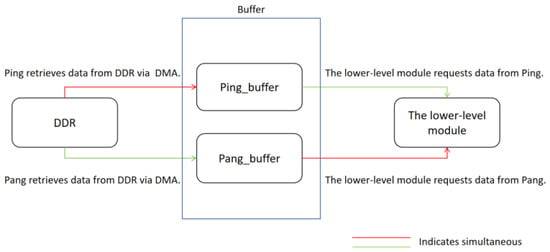
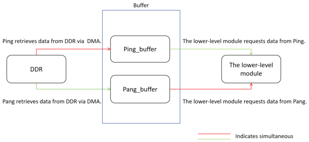
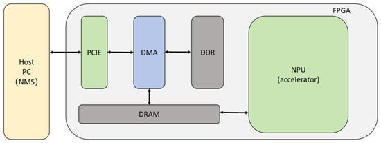
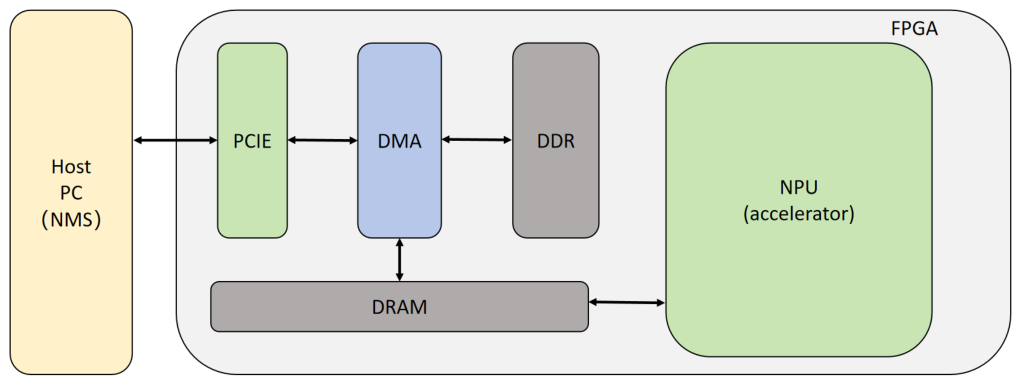
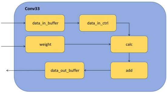
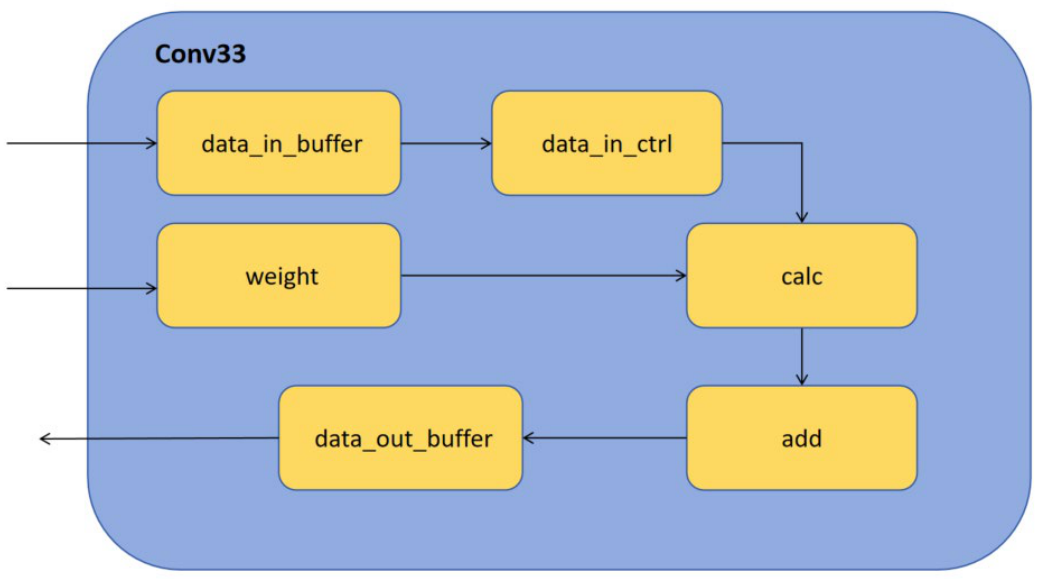
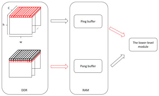
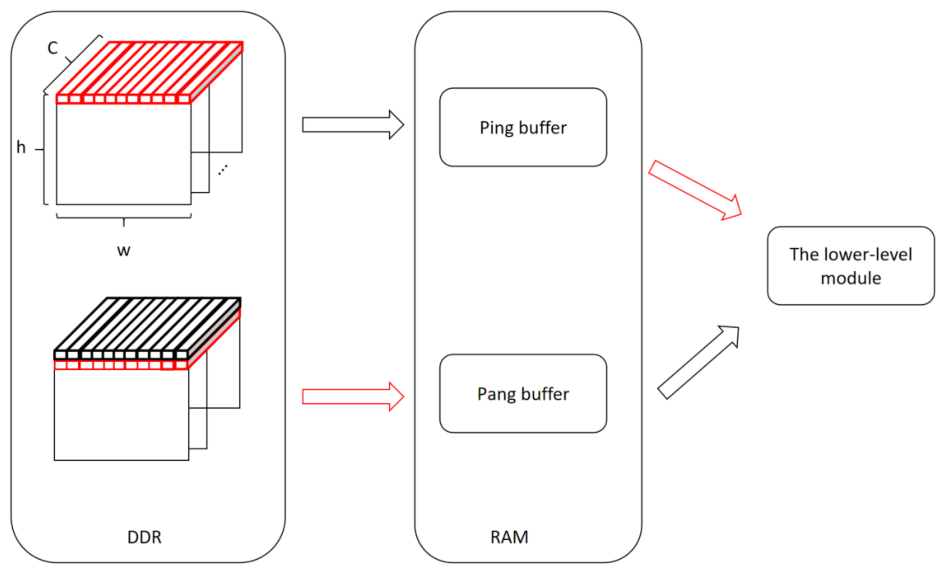
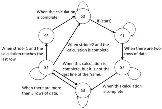
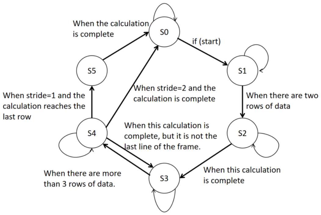
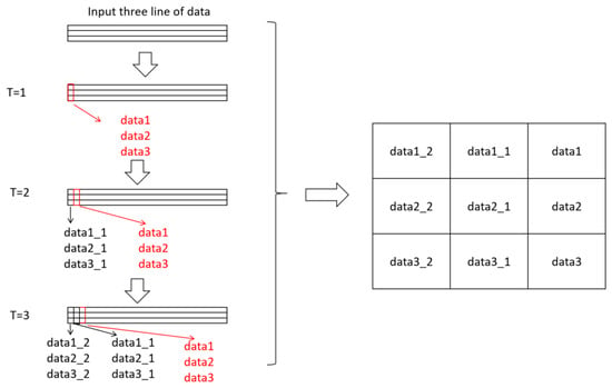
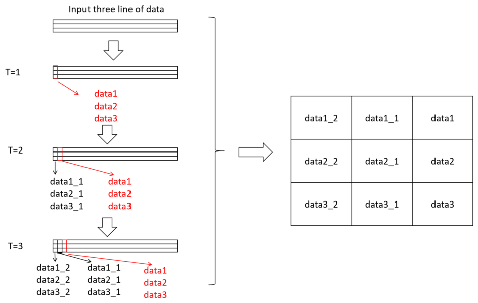
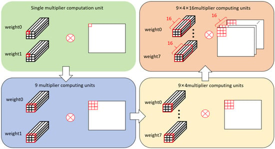
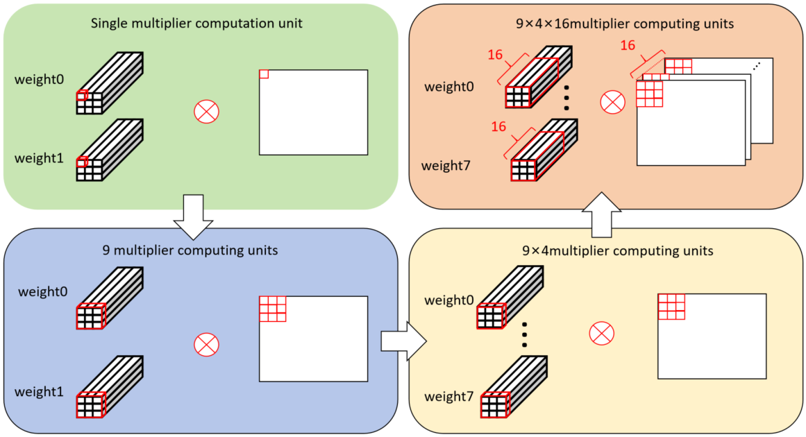
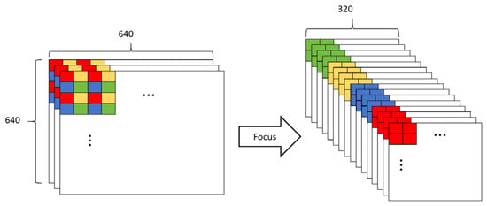
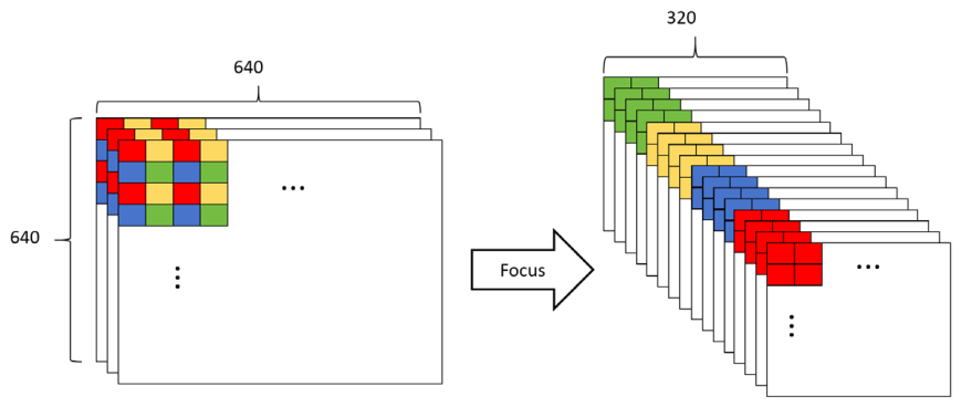
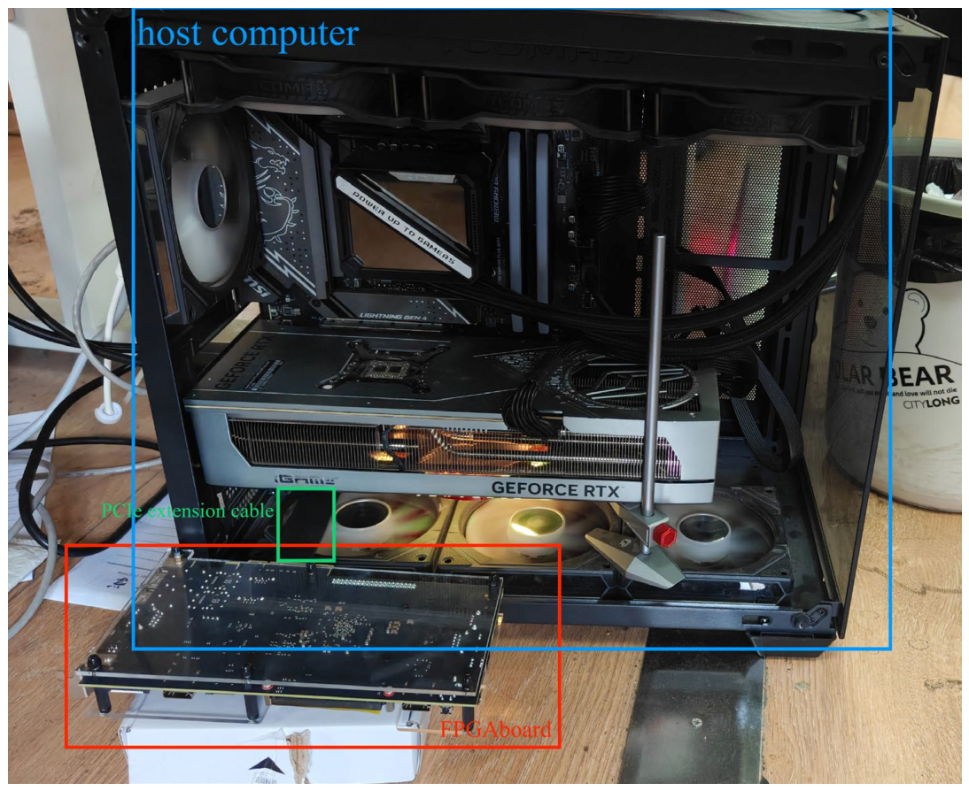
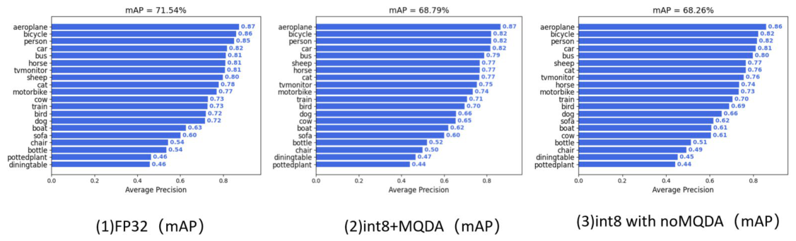
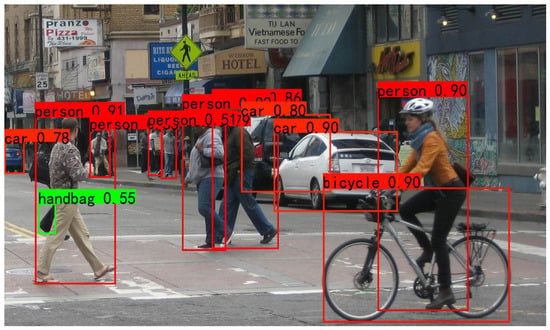
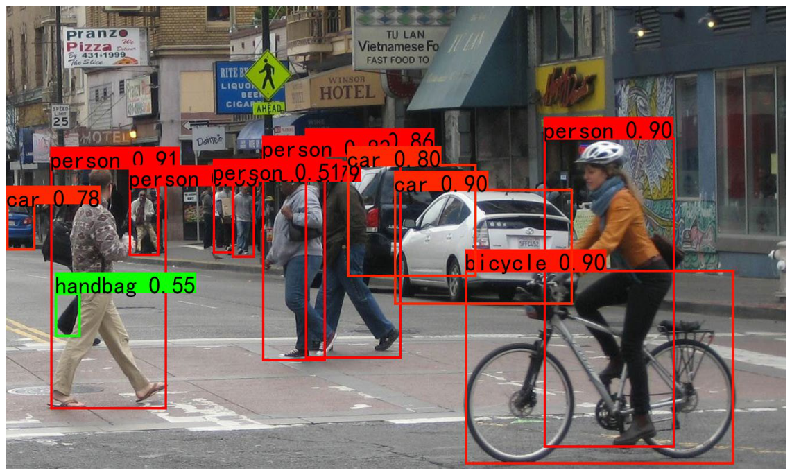

Disclaimer/Publisher’s Note: The statements, opinions and data contained in all publications are solely those of the individual author(s) and contributor(s) and not of MDPI and/or the editor(s). MDPI and/or the editor(s) disclaim responsibility for any injury to people or property resulting from any ideas, methods, instructions or products referred to in the content. |
© 2026 by the authors. Licensee MDPI, Basel, Switzerland. This article is an open access article distributed under the terms and conditions of the Creative Commons Attribution (CC BY) license.