


Abstract
This article proposes a bidirectional half-bridge resonant converter based on partial power regulation. The converter adopts an LLC converter as a DC-DC transformer (LLC-DCX) in the main power circuit and works in the open loop at the resonant frequency to give full play to the performance advantages of the LLC resonant converter. The partial power regulation circuit incorporates a synchronous Buck converter, enabling forward and backward power transmission by controlling the power flow direction. The converter achieves soft switching in both forward and backward directions, thereby reducing switching losses and enhancing conversion efficiency. Compared with the LLC-DCX converter, this converter can achieve wide voltage gain regulation while having high efficiency, which makes it suitable for charge–discharge applications between energy storage systems and DC Buses. In order to verify the performance of the proposed converter, a 1 kW prototype was constructed, maintaining a constant primary voltage of 400 V and a secondary voltage range of 350 V to 450 V. Experimental results indicate that the prototype achieves peak efficiencies of 97.74% in forward operation and 96.92% in backward operation, thoroughly demonstrating the feasibility and effectiveness of the proposed converter.
1. Introduction
In recent years, DC/DC converters have developed rapidly, playing a crucial role in various fields such as renewable energy, electric vehicles, energy storage systems, and DC microgrids [1,2,3]. In many applications of electric vehicles and energy storage systems, DC/DC converters are required to function across an extensive range of voltage gains. The LLC resonant converter is favored for its straightforward design, the ease with which it achieves soft switching, and its high power density [4,5,6]. LLC resonant converters mostly adopt pulse frequency modulation (PFM), but the contradiction between wide gain regulation and high efficiency are still prominent [7,8]. Therefore, experts and scholars have improved the topology, control methods, and parameter optimization to ensure that LLC resonant converters can operate with high efficiency across a broad voltage gain range.
To address the challenges mentioned, refs. [9,10] introduce a hybrid control strategy that integrates Phase Shift Control (PS) with Pulse Width Modulation (PWM). This approach notably enhances the operational performance of the LLC resonant converter. Nonetheless, at low input voltage, the LLC resonant converter has limited output voltage variation and reduced flexibility. This results in higher peak currents on the primary and secondary sides, causing greater power losses. Moreover, an excessively large phase shift angle may force the lagging leg of the bridge into hard-switching conditions. Alternative solutions presented in [11,12,13] employ a hybrid control method of PWM and PFM. By incorporating two distinct control parameters, this method aims to refine the converter’s operational characteristics. However, this hybrid control technique may cause transformer bias and increase switching losses. Furthermore, it will increase the complexity of control. It also necessitates a reevaluation of the soft-switching conditions for the switching transistors during the design phase. The strategies outlined in [14,15] utilize a combination of PFM and Pulse Skip Modulation (PSM) control. This method can realize the wide voltage range regulation of the LLC resonant converter.
The topology of the LLC resonant converter has also been improved in terms of variable structure, changing the resonant network, and adding auxiliary switches [16,17,18,19,20,21,22]. In [16,17], the converter alternates between full-bridge and half-bridge topologies by rearranging the switching devices, thereby achieving a multi-mode operation and expanding the voltage regulation capabilities. Ref. [17] demonstrates a hybrid multi-mode converter, which can realize ultra-wide voltage regulation; ref. [18] introduces additional switching elements on the secondary side to realize three rectification modes. This diversity in switching patterns extends to a range of gains, enhancing the converter’s adaptability. Ref. [19] takes a hybrid approach by paralleling two LLC resonant converters on the primary side and incorporating an extra switch on the secondary side. Wide voltage gain can be realized by switching between different operation modes. While these topological innovations effectively extend the operational scope of the converter, they also present certain trade-offs. The utilization rate of components may diminish, potentially leading to a decrease in power density. Furthermore, the uneven distribution of operational load among components could compromise the system’s longevity and reliability, as some elements may experience more wear and tear than others. These considerations are crucial for maintaining the balance between performance enhancement and the practical implications of the converter’s overall efficiency and durability.
In [20,21,22], a proposal has been made to augment the third winding of the transformer with an auxiliary LC resonant circuit, thereby altering the equivalent excitation inductance and widening the converter’s gain. However, the introduction of a third winding in this method leads to increased core loss and resonant current. Additionally, there exists the potential risk of a short circuit occurring due to the zero impedance of the auxiliary LC circuit at the resonant frequency.
Since the two-stage structure may reduce the overall conversion efficiency and power density, refs. [23,24] propose a quasi-single-stage converter with partial power regulation. This converter effectively achieves high-efficiency operation by directly transmitting most of the power to the load. At the same time, a small part of the power is handled by the auxiliary circuit to achieve voltage regulation, thus improving the overall efficiency. However, it is difficult to achieve soft-switching of the auxiliary circuit in the converter as described in [23,24]. This will reduce the efficiency and cause EMI (Electromagnetic Interference) noise.
By improving the control method and topology structure, the voltage gain range of the LLC resonant converter is improved to some extent. Nevertheless, it is challenging for single-stage LLC resonant converters to simultaneously achieve high frequency, high efficiency, and a wide gain range. Some scholars proposed a two-stage LLC converter structure to expand the gain range of the LLC resonant converter. Refs. [25,26,27,28] investigated an integrated quasi-two-stage Buck-LC converter, which adjusted the voltage by changing the voltage of the output capacitor of the quasi-front stage and improved the power density by bridge arm integration. The quasi-front circuit can adjust the total gain. However, there is higher cycling power in this structure, which leads to additional losses. In [29], a combination of an LLC resonant converter and Buck converter is proposed. The upper part of the structure is an LLC resonant converter, which operates as a DCX for higher efficiency and handles most of the power. The lower part is the Buck converter, which realizes the dynamic voltage regulation of the system by processing part of the power. Low loss is maintained while extending the converter gain range. However, this topology is not suitable for areas requiring electrical isolation and a wide range of voltage gain regulation. Ref. [30] proposes a converter that combines a leg from a front-stage four-switch Buck–Boost (FSBB) circuit with a leg from a back-stage CLLC circuit. Ref. [31] integrated the PWM converter with the LLC converter into a multi-port converter and the magnetized inductance of the transformer as the filter inductance of the PWM converter to reduce the circuit volume. This integration aims to decrease the quantity of switching components, thereby enhancing the converter’s overall efficiency and power density, but it increases the complexity of control.
In addition, bidirectional DC/DC converters are also the focus of research today. In [32], a control method of a PS-PWM CLLC bidirectional resonant converter is discussed, which adds a secondary capacitor to enable the converter to operate in both step-down and step-up modes. However, in bidirectional operation, the differences in resonant networks lead to asymmetrical operating characteristics, which poses a major challenge to parameter design. To solve this problem, refs. [33,34] studied the symmetric structure of a CLLC bidirectional resonant converter. Although this structure improves the symmetry of the operating characteristics to a certain extent, its gain does not decrease significantly when the gain is less than 1, which limits its application in a wide voltage range.
This paper presents a new design for a bidirectional resonant converter that is based on the principle of partial power processing. It aims to expand the voltage gain range of the LLC converter. This design is capable of meeting the charging and discharging requirements between energy storage batteries and DC Buses, offering substantial benefits such as increased efficiency and a wide gain range. Within this framework, the main power pathway incorporates an LLC converter operating at its resonant frequency to optimize the performance of the bidirectional converter. At the same time, the synchronous Buck converters are used to process partial power to control the output voltage.
The rest of this paper is organized as follows: Section 2 introduces the main power circuit system structure. Section 3 discusses the principle and analysis of the synchronous Buck voltage regulation circuit. The relevant parameter calculations are discussed in Section 4. The proposed conception is experimentally verified in Section 5.
2. The Structure of Partial Power Processing
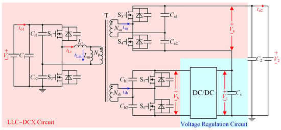
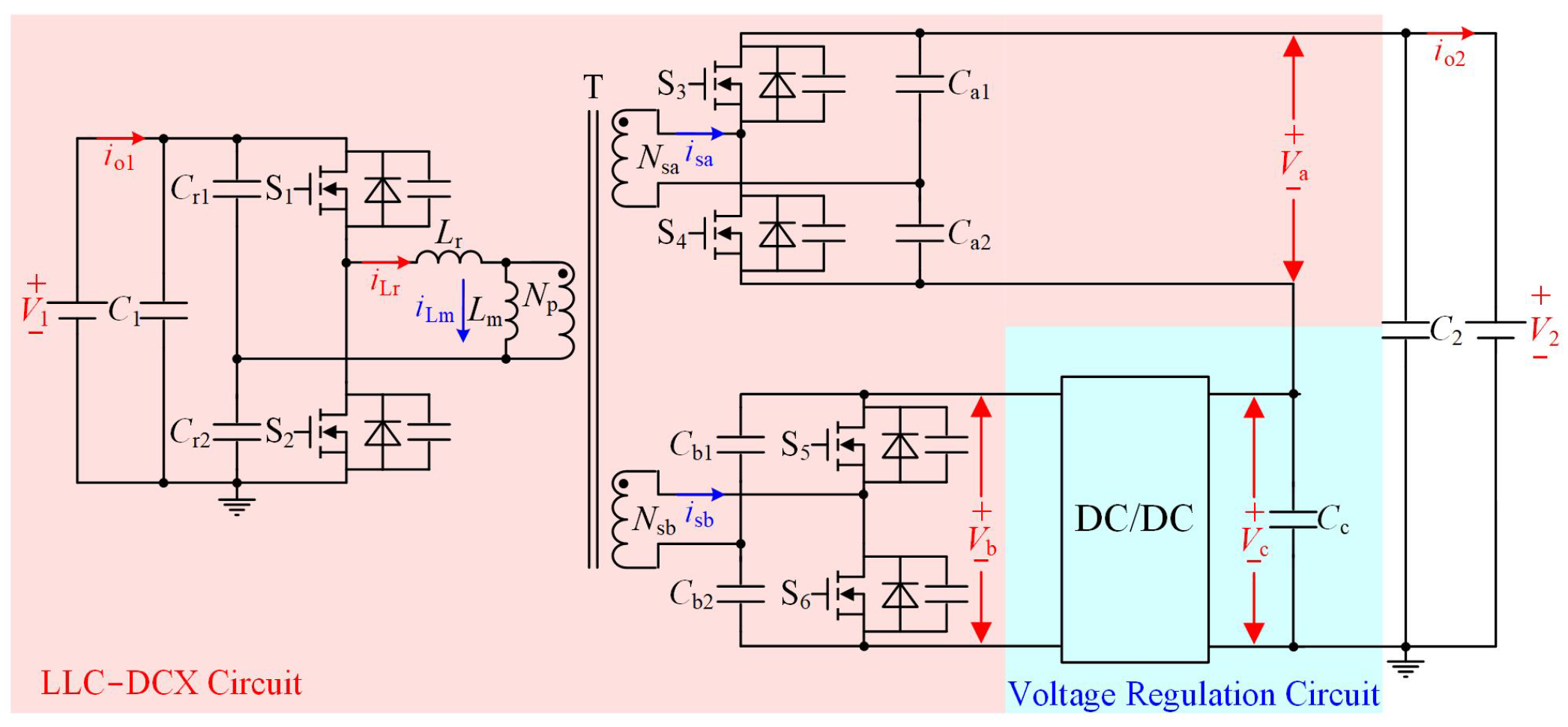
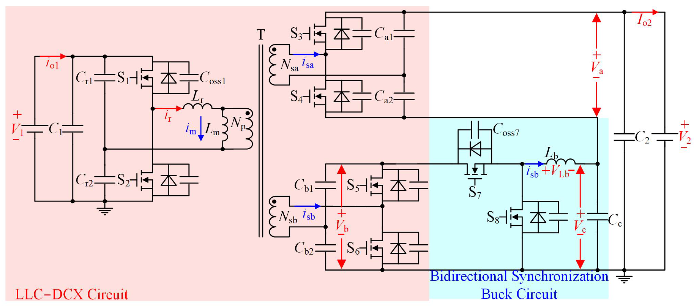
Figure 1 depicts the architecture of a partial power regulation converter, which consists of a main power circuit and a partial power regulation circuit. The main power circuit is an LLC resonant converter that operates in an open-loop state at the resonant frequency, resulting in a fixed gain and exhibiting DCX characteristics. The partial power regulation circuit is arranged in an input-parallel, output-series configuration with the main power circuit. The total output voltage of the converter is the sum of the output voltage from the main power circuit and the output voltage from the partial power circuit. By adjusting the output voltage of the partial power regulation circuit, the overall output voltage of the converter can be fine-tuned.
Figure 1.
Partial power regulation architecture.
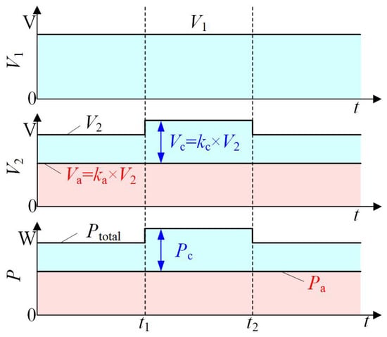
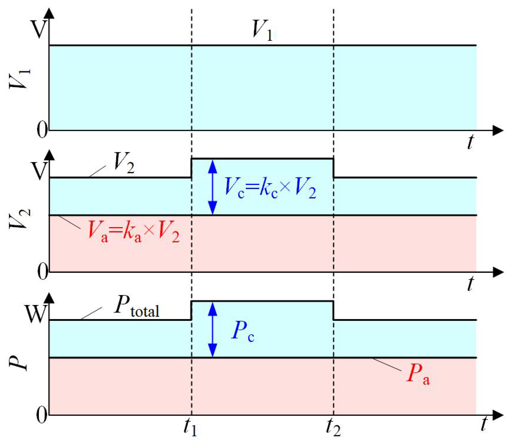
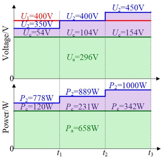
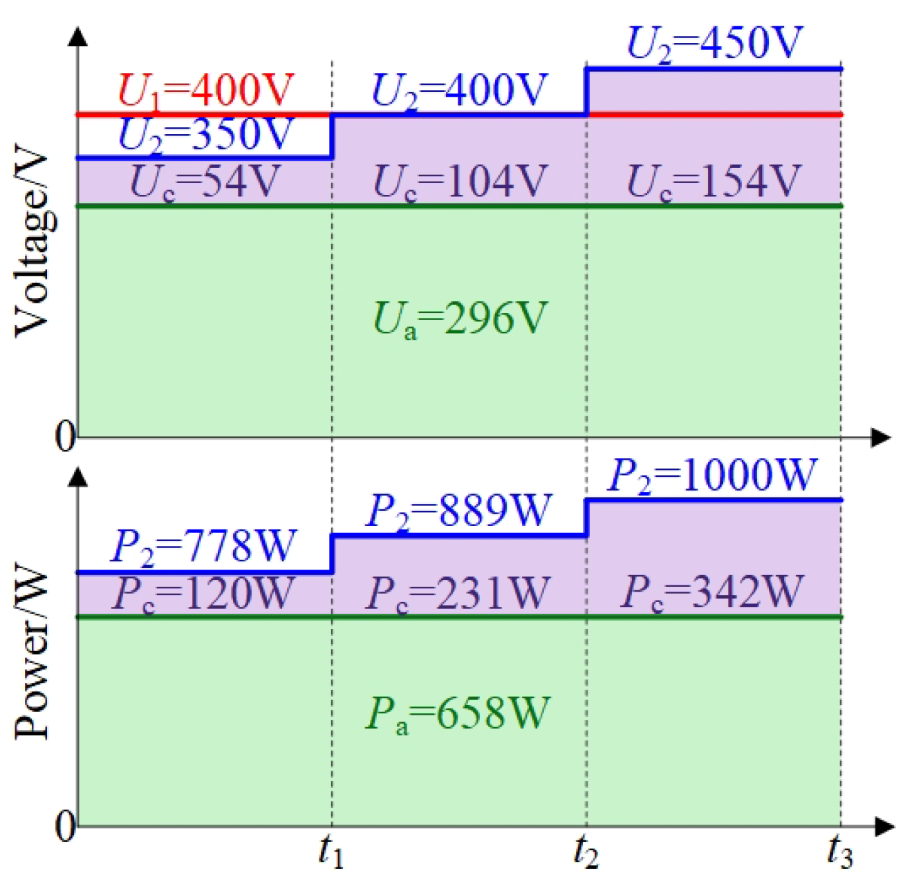
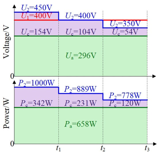
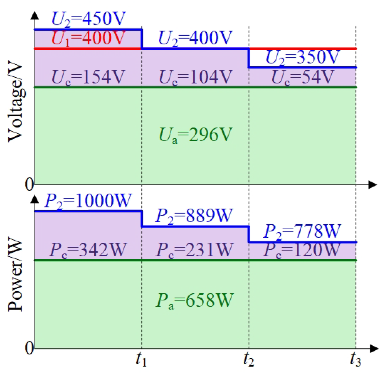
Figure 2 illustrates the power distribution between the main power circuit and the partial power regulation circuit of the converter. Taking the forward mode as an example, the input voltage to the converter is held constant. Given that the LLC resonant converter functions in DCX mode, its voltage gain is stable, which means the output voltage from the LLC converter does not fluctuate. The aggregate output voltage of the converter is modulated by the partial power regulation circuit.
Figure 2.
Voltage and power distribution of the converter.
is the main power circuit power, is the partial power regulating circuit power, then the total power transmitted by the converter is
Let and , where represents the ratio of the main power circuit’s output voltage to the secondary-side voltage and represents the ratio of the partial power regulation circuit’s output voltage to the secondary-side voltage. It is given that . Considering that the efficiencies of the main power circuit and the partial power regulation circuit are and respectively, the overall efficiency of the converter can be formulated as
From the above equation, the total efficiency of the converter is calculated by weighting the efficiencies of both the main power circuit and the partial power regulation circuit. In the operation of the converter, the main power circuit is responsible for transferring the majority of the power, whereas the partial power regulation circuit is utilized for voltage adjustment and handles a smaller fraction of the power. In terms of power distribution, , which means that in terms of voltage distribution on the secondary side, . Therefore, the aggregate efficiency of the converter is predominantly influenced by the efficiency of the main power circuit’s LLC resonant converter. This underscores the significance of optimizing and enhancing the performance and efficiency of the LLC resonant converter.
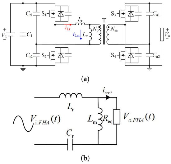
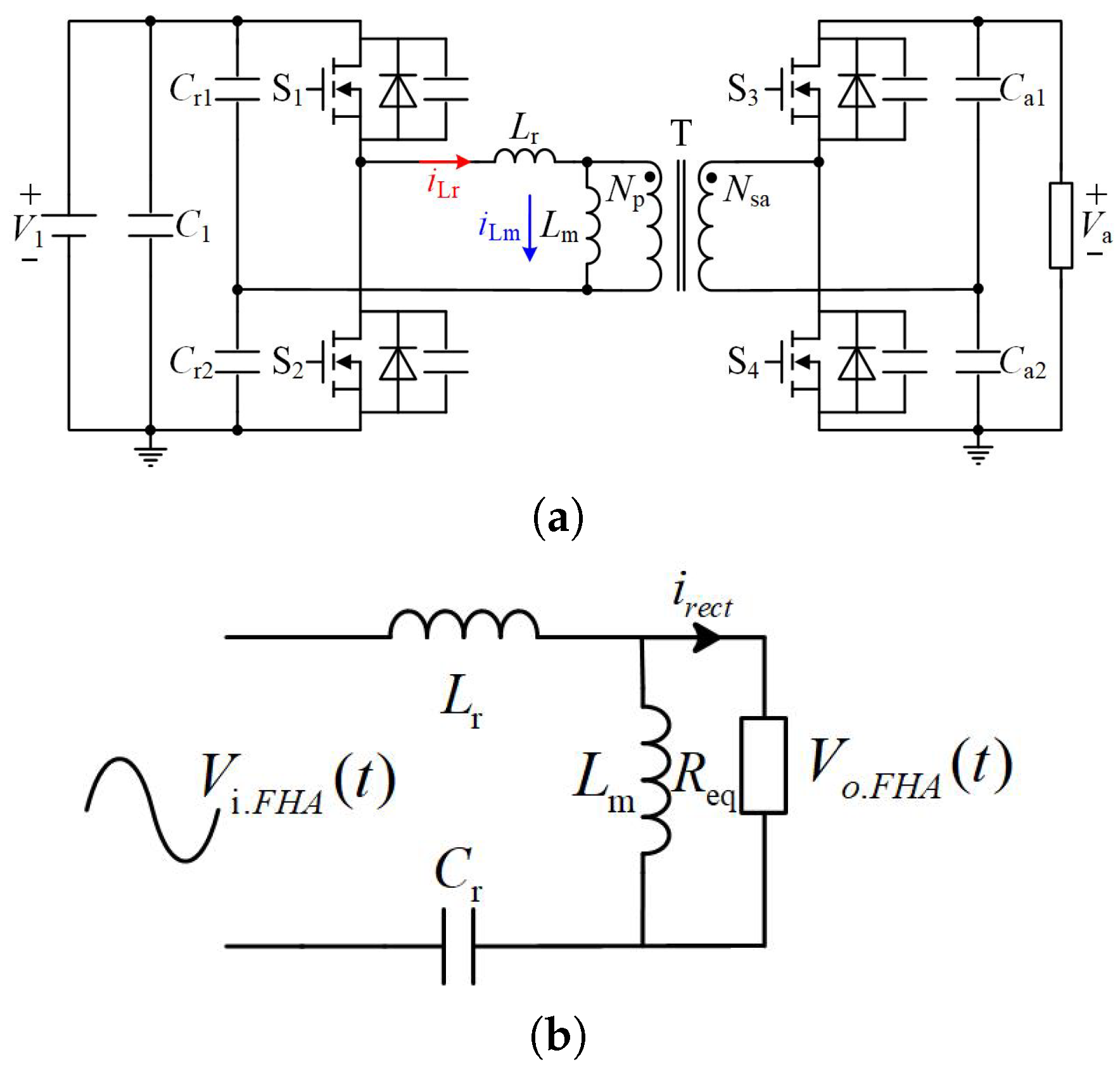
The main circuit adopts a split-capacitor LLC volt-doubling resonant converter, as shown in Figure 3a. This design approach divides the resonant capacitor typically found in an LLC converter into two equal series-connected capacitors. This modification weakens the input current ripple, results in a more sinusoidal resonant current waveform, and alleviates the voltage stress on the input capacitor. Compared with the high on-loss of the traditional rectifier mode, synchronous rectifier technology uses fully controlled devices with low on-resistance to replace the rectifier diodes. This reduces the on-loss and is conducive to achieving high-voltage output [35].
Figure 3.
Bidirectional half-bridge LLC resonant circuit (a) Main circuit topology. (b) LLC fundamental equivalent circuit.
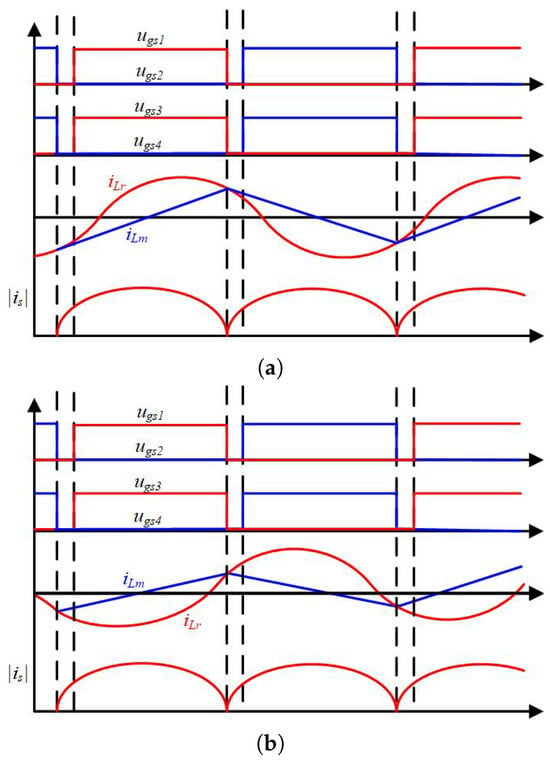
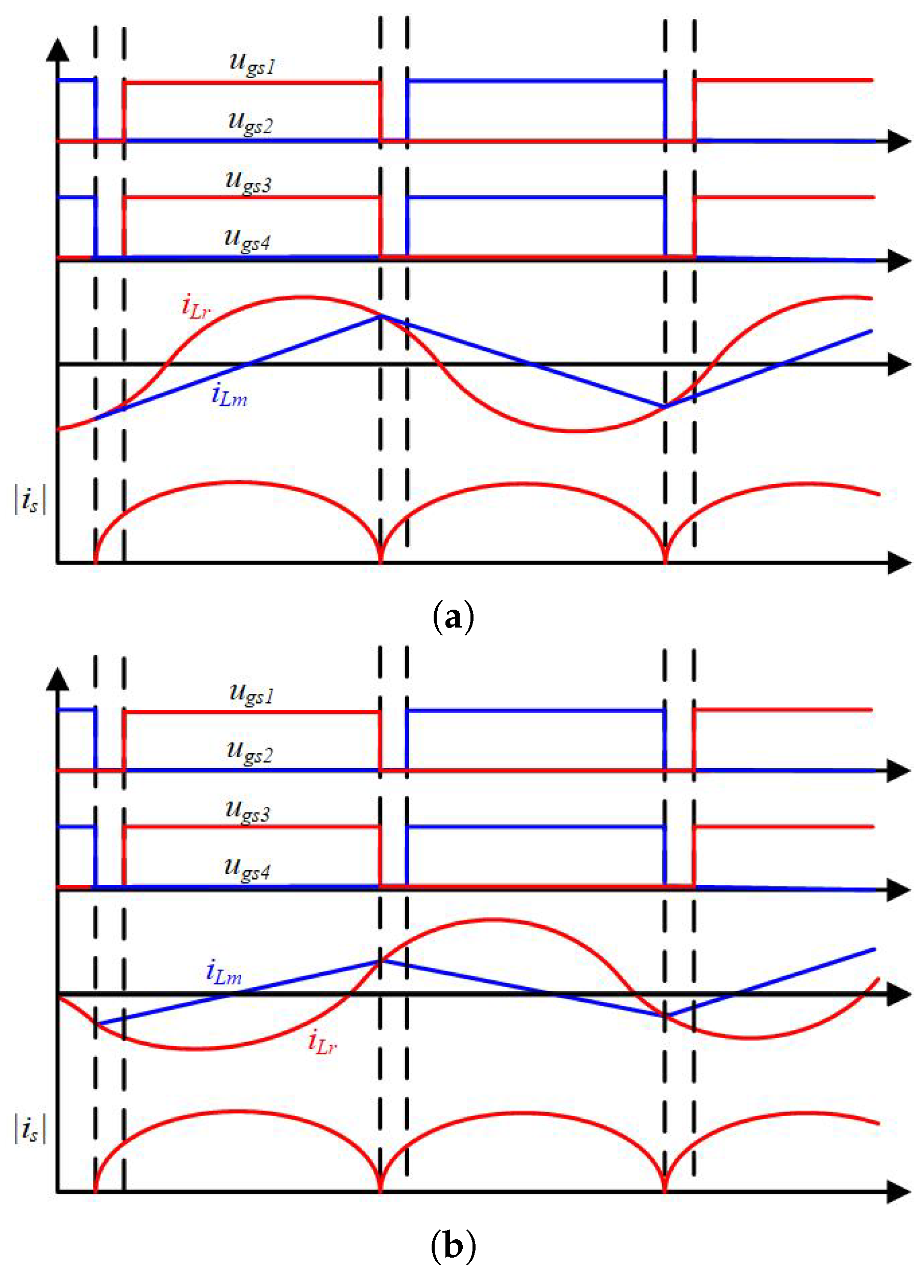
The key waveform of the split-capacitor LLC volt-doubling resonant converter operating in DCX mode is shown in Figure 4. In this mode, switches and can achieve ZVS and the current resonates at a smaller value when switched off. Switches and can implement ZCS without a backward recovery process. Operating at the resonant frequency offers several advantages. It enables the optimization of resonant parameters and the design of magnetic components. Moreover, it simplifies the driving logic for synchronous rectification.
Figure 4.
The main waveform of the split-capacitor LLC volt-doubling resonant converter. (a) Key forward waveform. (b) Key backward waveform.
The input voltage waveform and output voltage waveform of the resonant tank in Figure 3b can be expressed in Fourier series:
where is the amplitude square wave of the input voltage, is the switching frequency, and is the phase shift with respect to the input voltage.
Since the input current of the rectifier network is in phase with the input voltage, the fundamental-wave component can be derived from the effective value and phase of the input current of the rectifier network as follows:
where is the RMS value of the rectifier input current.
Since and are in phase, the rectifier block presents an effective resistive load to the resonant tank circuit, , equal to the ratio of the instantaneous voltage and current:
According to the FHA equivalent circuit, the transfer function of the converter is
According to the above equation, the normalized gain can be obtained [36]:
where k is the inductance ratio, is the normalized frequency, and Q is the quality factor.
When the LLC operates at the resonant frequency , the gain characteristic is almost independent of the switching frequency and load, exhibiting the characteristics of a DCX. In this scenario, the gain characteristic of the LLC-DCX converter is exclusively determined by the transformer’s turn ratio, denoted as and . Therefore, the gain of the LLC-DCX is related only to the transformer turn ratio:
Based on the analysis, the advantages of using a split-capacitor LLC voltage-doubling resonant converter in DCX mode are as follows:
- (1)
- The gain characteristic of the LLC-DCX converter is minimally affected by the switching frequency and load variations, allowing the main power circuit to maintain high efficiency across its entire operational range.
- (2)
- The LLC-DCX converter works in the inductive region and can achieve full-range ZVS. In theory, it is also possible to enhance efficiency by increasing the excitation inductance, thereby reducing circulating and conduction losses.
- (3)
- The LLC-DCX converter operates at the resonant frequency in an open-loop configuration, which simplifies the control algorithm and improves system consistency.
- (4)
- By operating solely at resonant frequency points, the LLC-DCX converter optimizes the design of magnetic components. This reduction in magnetic core volume leads to improved efficiency and power density.
3. Synchronous Buck Voltage Regulation Circuit
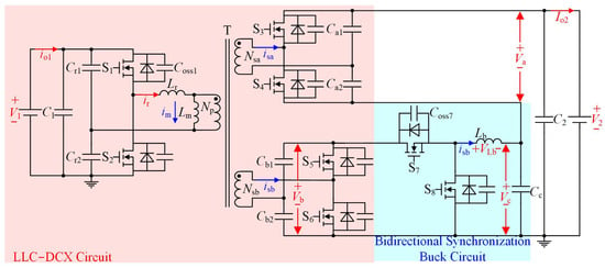
Building on the foundation of the LLC-DCX circuit, in order to broaden the gain range, a partial power regulation architecture is implemented, and a voltage regulator circuit is added. This results in a two-stage configuration that combines the DCX and the voltage regulator circuit. The front stage of the system employs the LLC-DCX circuit to meet the isolation requirements essential for the energy storage system. At the same time, the rear stage uses a non-isolated voltage regulator circuit to expand the gain range. As shown in Figure 1, with reference to the partial power regulation architecture, a synchronous Buck voltage regulator circuit operating in the Forced Continuous Conduction Mode (FCCM) is adopted, as further shown in Figure 5. Next, an analysis of the working principle and characteristics of the synchronous Buck converter under PWM control is presented.
Figure 5.
Partial power-processing bidirectional resonant converter architecture.
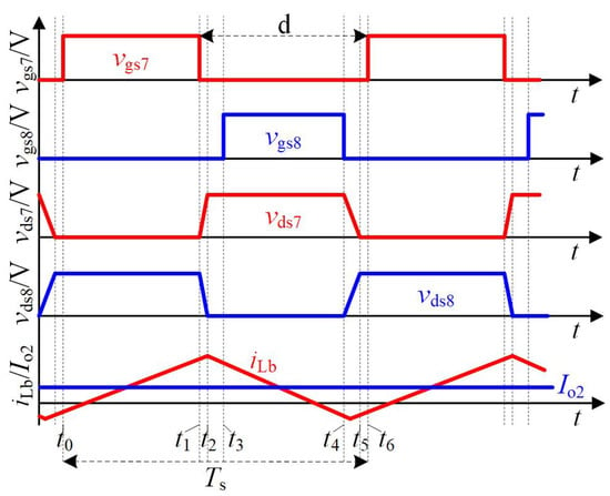
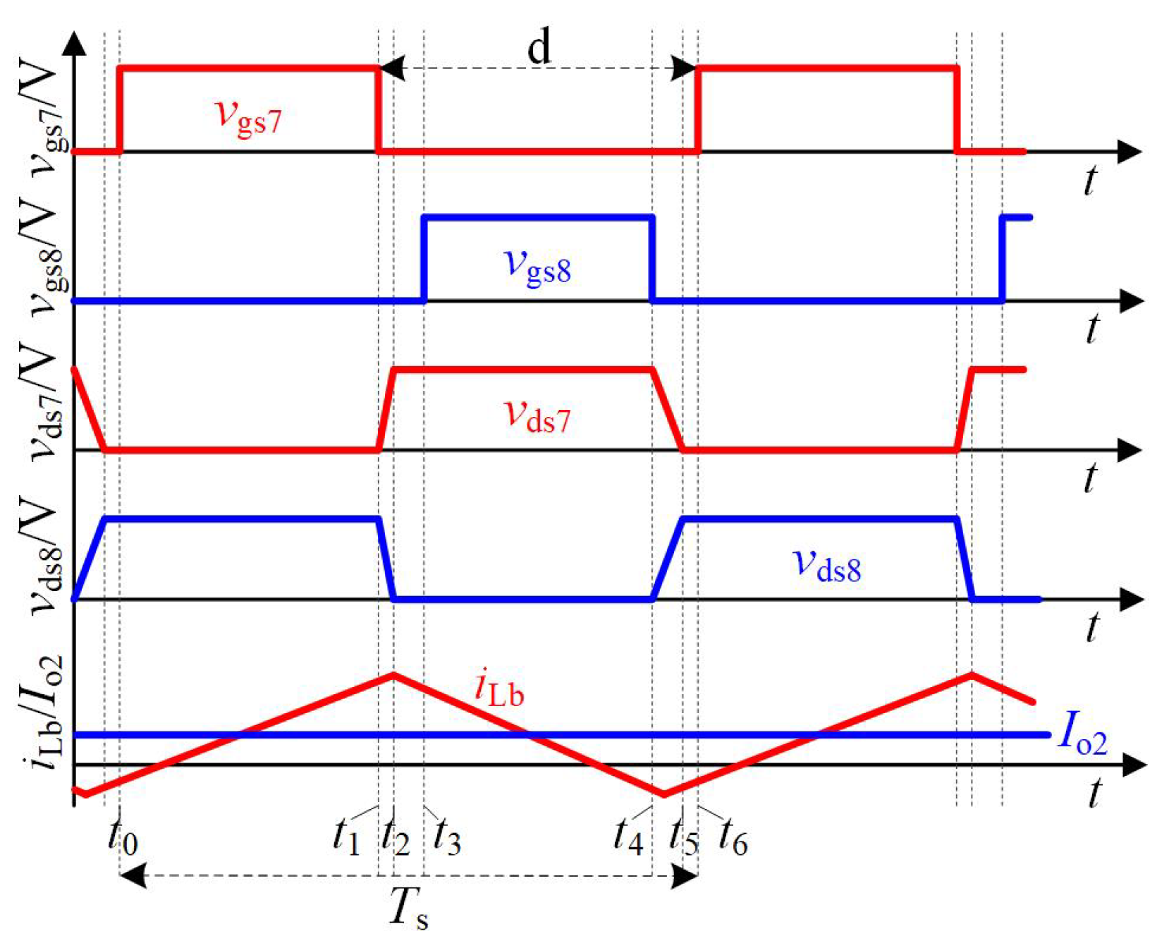
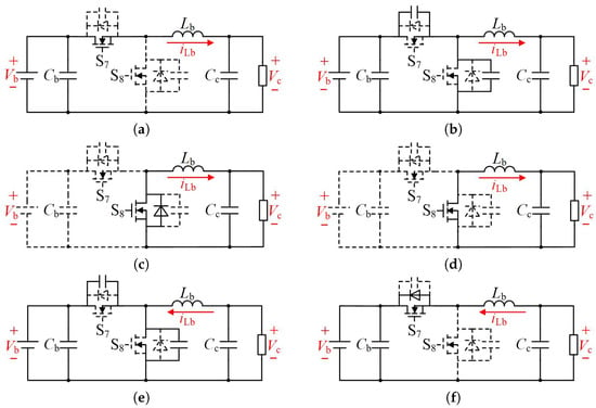
The essential waveforms of operation are depicted in Figure 6, where the working principle of the synchronous Buck converter in FCCM is analyzed. Throughout a single switching cycle, the converter’s corresponding operating modes are presented in Figure 7.
Figure 6.
Key waveform of Buck converter in FCCM mode.
Figure 7.
Mode of synchronous Buck converter in FCCM mode. (a) Mode 1 [, ]. (b) Mode 2 [, ]. (c) Mode 3 [, ]. (d) Mode 4 [, ]. (e) Mode 5 [, ]. (f) Mode 6 [, ].
Mode 1 [, ]: In this mode, the switch conducts, and the voltage across inductor , denoted as , is determined by the difference between the input voltage and the output voltage . During this phase, the inductor current rises linearly in the positive direction, transitioning from a negative value to a positive one. At , the transistor turns off. In this mode, the expressions for the change rate of inductance voltage and inductance current are
Mode 2 [, ]: At , is turned off, and the inductance current is positive. In this mode, the inductance current charges the capacitor at the junction of and discharges the capacitor at the junction of . The drain voltage at both ends of drops to zero.
Mode 3 [, ]: When the drain-source voltage across drops to zero, the body diode of conducts, clamping the drain voltage to zero, which creates conditions for to achieve ZVS.
Mode 4 [, ]: The driving signal of arrives to achieve ZVS, the voltage across the inductor is the output voltage , the inductance current linearly decreases until it crosses zero and becomes negative, and turns off. In this mode, the expression for the change rate of inductance voltage and inductance current is as follows:
Mode 5 [, ]: At , the direction of the inductor current is negative, causing discharge of the junction capacitor and discharge of the junction capacitor. The drain voltage at both ends of the junction decreases to zero.
Mode 6 [, ]: When the voltage across the leakage inductance at the terminals of switch drops to zero, the body diode of conducts, clamping the drain source voltage at zero, which creates conditions for to achieve ZVS.
Based on the balance of the volt-second product for inductance, the gain characteristics of the synchronous Buck converter are derived by correlating Equations (12) and (14):
where represents the gain of the synchronous Buck converter, and d is the duty cycle of the switch .
Equation (15) demonstrates that the voltage gain of the synchronous Buck converter is directly proportional to the duty cycle d of switch . Therefore, for the synchronous Buck converter, switches and are modulated using only PWM control.
From (8) and (15), the voltage gain of the partial power regulation circuit using the synchronous Buck voltage regulation is
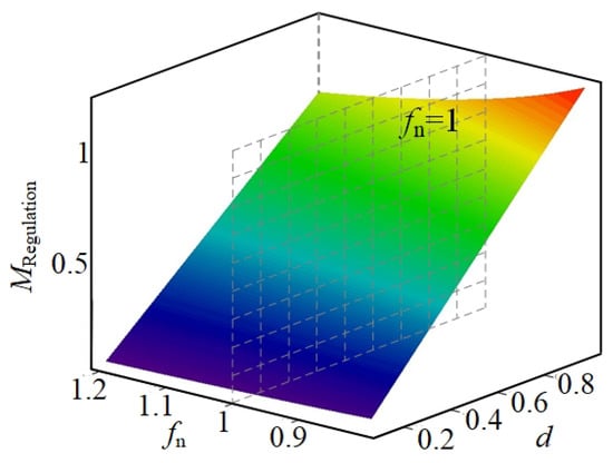
The gain characteristics of part of the power-regulating circuit are drawn from (16), as shown in Figure 8. At this time, the inductance ratio and the quality factor . It is evident that when the LLC converter operates at the resonant frequency, the gain of the partial power regulation circuit can be extended by adjusting the duty cycle d of the synchronous Buck circuit. Consequently, this enhances the overall gain regulation range of the converter.
Figure 8.
Partial power regulation circuit gain characteristic diagram.
Compared to the Continuous Conduction Mode (CCM) mode and Discontinuous Conduction Mode (DCM) mode used in traditional Buck converters, the FCCM mode used in the synchronous Buck converter in this paper can force the inductor current to flow in the opposite direction, providing conditions for and to achieve ZVS. Taking the forward working mode as an example, the average inductance current of the synchronous Buck converter is
where is the secondary-side current of the converter, and is the increment of inductance current:
The maximum value of inductance current and the minimum value of inductance current are
Based on the operational analysis of the synchronous Buck converter, it is observed that the minimum inductor current charges and discharges the junction capacitor of switch , facilitating soft-switching conditions for . Similarly, the maximum inductor current charges and discharges the junction capacitor of switch , facilitating soft-switching conditions for . Given the differing conditions required for soft switching between and , achieving soft switching for is comparatively more challenging than for . Hence, the primary focus should be on the implementation conditions for soft-switching for .
The limit condition for to achieve soft switching is that the voltage at both ends of the junction capacitor is exactly zero. At this time, resonance occurs between the inductor and the junction capacitor, and there are
where is the dead time of the driving signal of the switching.
Based on the analysis of the working principle and soft-switching characteristics of the bridge synchronous Buck converter, a reasonable inductance value is designed and selected. This enables the synchronous Buck converter to operate in FCCM mode, providing conditions for soft switching of and to further reduce switching losses and improve the overall efficiency of the converter.
4. Parameter Design
4.1. ZVS Condition
When switches operate under hard-switching conditions, they incur substantial switching losses. Therefore, soft-switching techniques are essential to enhance the overall efficiency of the system. The switch devices to consistently operate at a 50% duty cycle with complementary conduction, and the working characteristics of the three bridge arms are identical, to simplify the analysis. It is only necessary to analyze the soft switching of one switch device.
Taking switch devices and as an example, during the forward operation mode of the converter, the resonant current is negative, which charges the junction capacitance of switch device . As the drain-source voltage of switch device increases to the primary-side voltage , the junction capacitance of switch device discharges until the drain-source voltage of switch device drops to zero. At this point, a drive signal is applied to switch device , and switch device achieves ZVS.
The dead time of the drive signals for switch devices and is set as , the junction capacitance of the switch device is , and the operating cycle is . Since the voltage across the two partial windings on the secondary side is equivalent to the voltage across the primary-side excitation inductance , the voltage across can be approximated as . The relationship between the voltage and current on the excitation inductance is
When the switch is turned off, the excitation current value is , which provides conditions for the soft switching of the switch .
According to the implementation conditions of switching ZVS, the excitation inductance needs to meet
4.2. Circuit Parameter Design
- (1)
- Synchronous Buck circuit parameter design
According to the third section of this article, when operating in FCCM, the converter can force the inductor current to flow in the backward direction, thus creating conditions for switch devices and to achieve ZVS. The minimum inductor current enables soft switching for switch device by charging and discharging its junction capacitance. Similarly, the maximum inductor current enables soft switching for switch device through the same charging and discharging process of its junction capacitance. Since the conditions for switch devices and to achieve soft switching differ, it is more difficult for switch device to achieve soft switching than for switch device . Therefore, the main consideration is the condition for to achieve soft switching. From (17), (18), and (20), the minimum inductance current is
The limiting condition for the switch to achieve soft switching is that the voltage across the junction capacitor is exactly zero. At this time, the inductor and the junction capacitor resonate, then
In the formula, represents the dead time of the drive signals for switches and . To ensure that soft switching of the switches can be achieved, the actual value of the inductance should be less than the value calculated by Equation (29). However, an excessively low value of can cause an increase in the reverse current flowing through the inductor. As a result, the RMS (Root-Mean-Square) value of the current passing through the switch will increase. This increase can have a negative impact on the overall efficiency of the converter.
- (2)
- Transformer turn ratio design
Based on the operational parameters of the partial power-adjusted bidirectional resonant converter presented in Table 1, when the converter operates in the forward mode, the 400 V DC voltage bus charges the energy storage system. Considering the charging and discharging characteristics of the battery, the output voltage needs to be regulated within the range of 350–450 V. In backward operation, the requirements for parameters on the primary and secondary sides remain unchanged.
Table 1.
Operation parameters of converter.
When the LLC-DCX converter operates in an open-loop configuration near the resonant frequency point and the normalized gain remains constantly at 1, the converter exhibits optimal operating characteristics and the simplest control scheme. The voltage gain of LLC-DCX is
The overall voltage gain of the converter is
According to the operational indicators of the converter, the gain range of the converter is
By substituting the voltage gain range of the synchronous Buck converter into (34), the following is obtained:
From Equation (35), it can be derived that , where d represents the on-duty ratio of switch . To fully leverage the degree of freedom of d, it is essential to maximize the adjustment range for achieving higher precision control. Through simulation analysis, the duty cycle d in this paper ranges from 0.28–0.8. The transformer ratio and can be calculated.
5. Experimental Verification
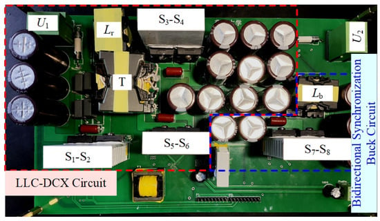
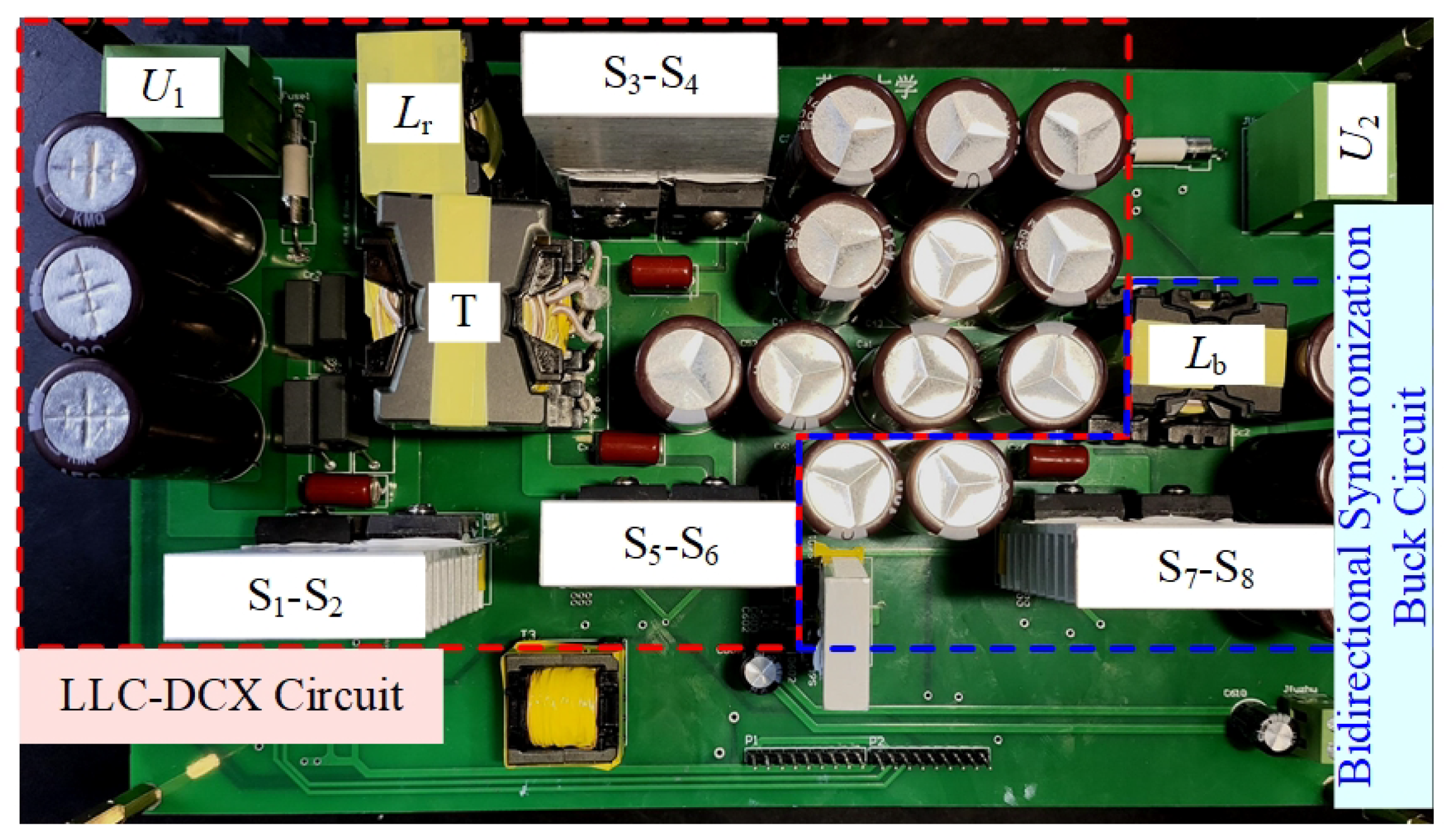
Based on the parameter design detailed in Section 4 and as presented in Table 2, an experimental platform with a capacity of 1 kW was constructed for the proposed converter, as depicted in Figure 9. Subsequently, experiments were conducted on this platform. To verify the gain and efficiency characteristics of the partially power-regulated bidirectional resonant converter based on synchronous Buck regulation in forward mode and backward mode, an experimental platform is built and relevant tests are carried out.
Table 2.
Converter simulation and experimental parameters.
Figure 9.
Photograph of the designed converter prototype.
5.1. Forward Mode
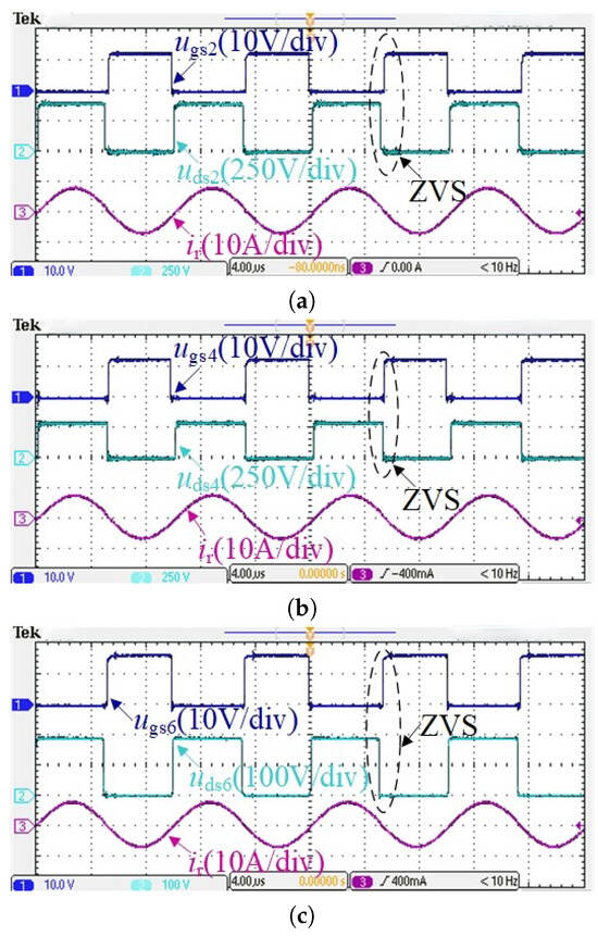
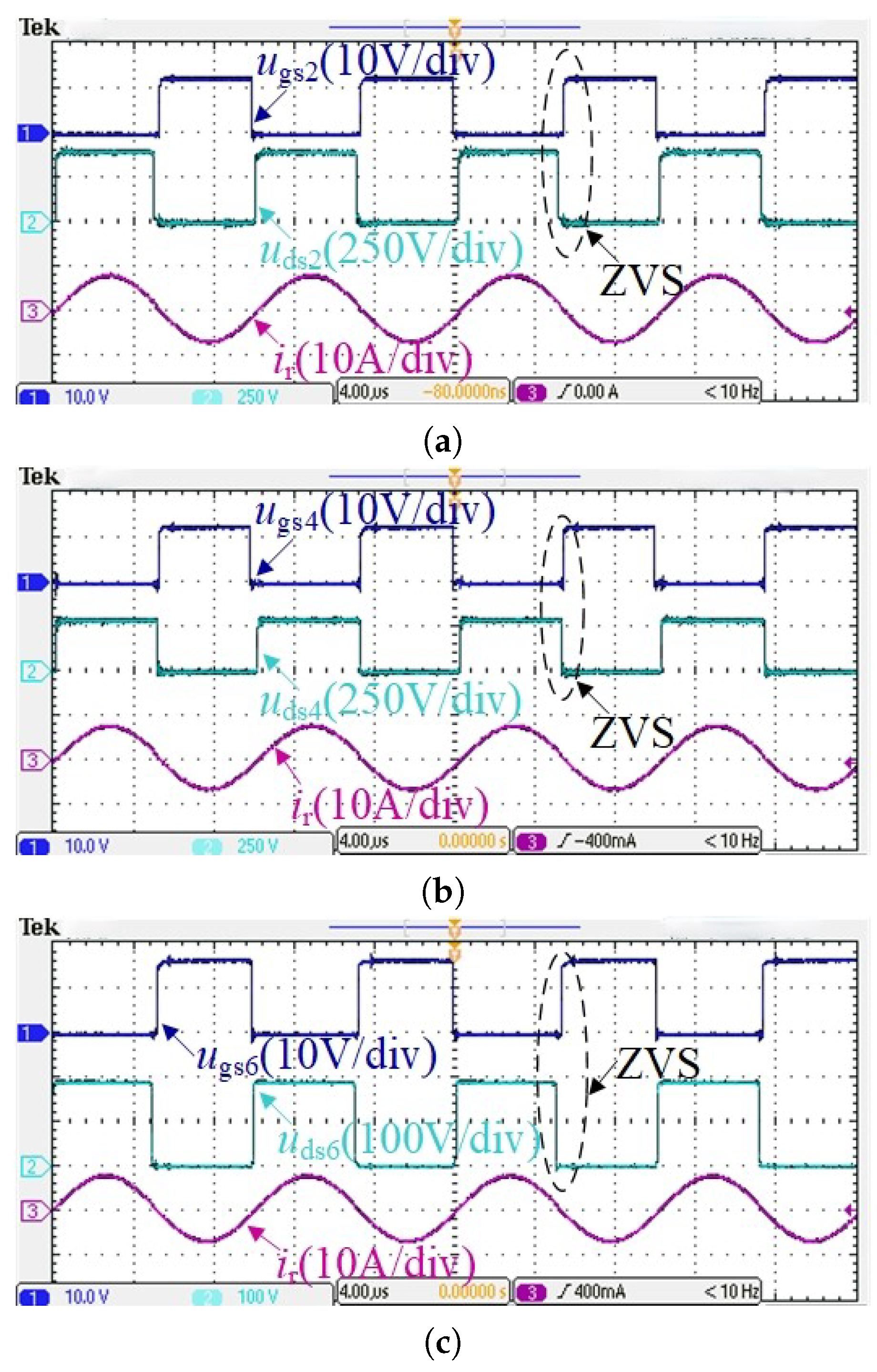
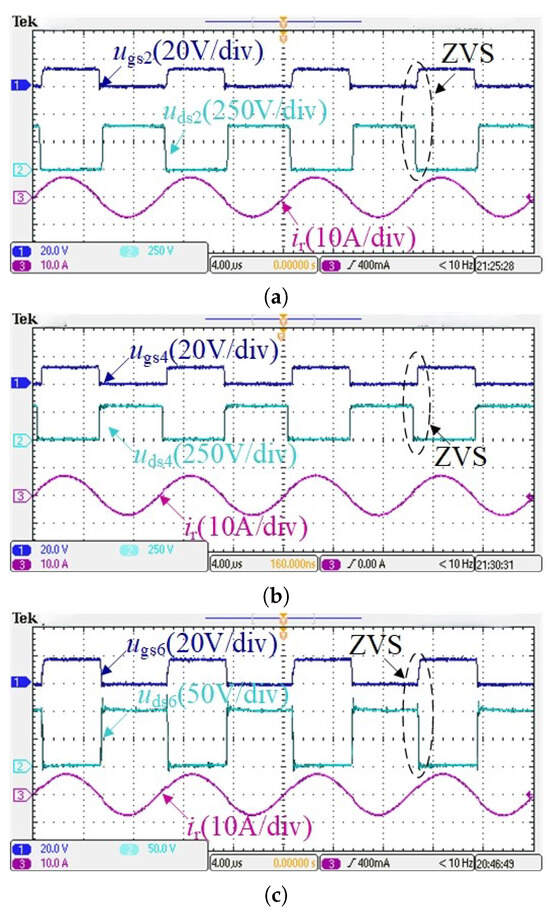
In the forward mode, the LLC-DCX converter operates at a resonant frequency of 100 kHz, with a primary input voltage of 400 V. It is designed to provide a secondary output voltage ranging from 350 V to 450 V. Among these switches, to operate in an alternating conduction mode with a 50% duty cycle. Switches and operate in a complementary conduction mode, and , , , and conduct in the same phase. Figure 10 shows the key waveforms of the LLC-DCX at an output of 400 V/2.22 A in the forward mode.
Figure 10.
The key waveforms of the LLC-DCX circuit under the output condition of 400 V/2.22 A. (a) Key waveforms of and resonant current. (b) Key waveforms of and resonant current. (c) Key waveforms of and resonant current.
In this operational mode, when the drain-source voltage of the primary-side switch in the LLC-DCX converter reaches zero, the gate-source voltage starts to increase, which facilitates ZVS. On the secondary-side main power circuit, switch and the power regulation circuit switch start to conduct once their drain-source voltages drop to zero, enabling ZVS. The voltage of the secondary double-voltage rectifier is divided according to the transformer’s design ratio. The voltage downstream of the main power circuit is 296 V, while the voltage after the partial power regulation circuit is 191 V.
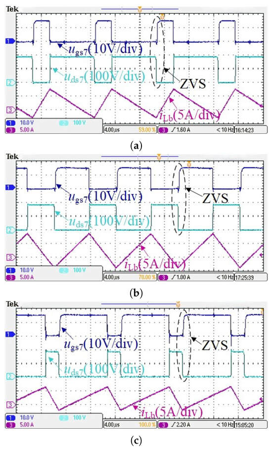
Figure 11 shows the critical waveforms of the synchronous Buck circuit under various output voltages. Within the secondary output voltage range of 350 V to 450 V, the output voltage is regulated by adjusting the duty cycle of switch . As shown in Figure 11a, when the secondary side outputs 350 V/2.22 A, the output power is 777.8 W, and operates at an on-duty ratio of 0.287. Switches and are activated alternately. The experimental waveforms indicate that after the drain-source voltage of drops to zero, the gate-source voltage starts to rise, thus achieving ZVS. At the same time, the inductance current of the Buck circuit drops to zero and the energy flows backward, which provides the conditions for the soft switching of the switches.
Figure 11.
The key waveforms of synchronous Buck circuit under different output voltages ( = 2.22 A). (a) and inductor current waveforms ( = 350 V). (b) and inductor current waveforms ( = 400 V). (c) and inductor current waveforms ( = 450 V).
When the secondary-side output is 400 V/2.22 A, the output power is 888.9 W. The duty cycle of is 0.55, and and conduct alternately. The pivotal waveform of the Buck circuit is depicted in Figure 11b, where switch achieves ZVS. When the secondary-side output is 450 V/2.22 A, the output power is 1 kW. The duty cycle of is 0.8, and and alternate conduction. The essential waveform of the Buck circuit is presented in Figure 11c, demonstrating that switch accomplishes ZVS.
In summary, the partial power-processing resonant converter, which incorporates a synchronous Buck voltage regulation circuit, is capable of adjusting the secondary output voltage to fall within the 350–450 V range during forward operation. In the forward mode, all switches within the converter are able to achieve ZVS across various operating conditions. This capability reduces the switching losses associated with the switches and, in turn, enhances the overall efficiency of the converter.
5.2. Backward Mode
In the backward mode of operation, the converter works at a resonant frequency of 100 kHz, with the secondary-side voltage maintained between 350 V and 450 V. The primary-side output voltage is kept constant at 400 V. The backward output power varies from 778 W to 1000 W, gradually decreasing as the secondary input voltage diminishes. The switching devices to operate in an alternating conduction mode with a 50% duty cycle, while and operate in a complementary conduction mode, and , , , and conduct in phase. Figure 12 presents the critical waveforms of the LLC-DCX converter operating in backward mode with a 400 V input and a 400 V/2.5 A output. Meanwhile, Figure 13 depicts the essential waveforms of the Boost circuit under various input voltage conditions.
Figure 12.
The key waveforms of the LLC-DCX circuit under the output condition of 400V/2.22A. ( = 400 V). (a) Key waveforms of and resonant current. (b) Key waveforms of and resonant current. (c) Key waveforms of and resonant current.
Figure 13.
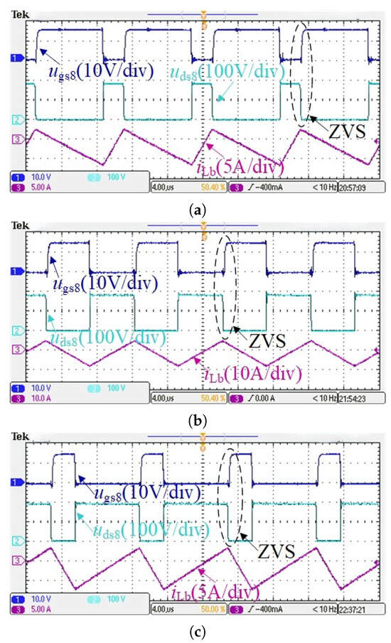
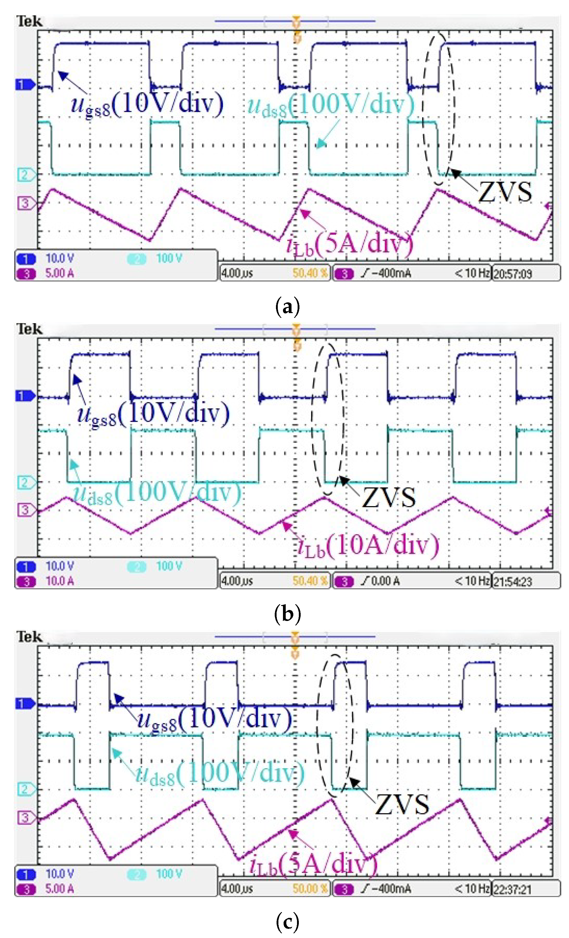
The key waveforms of the synchronous Boost circuit with different input parameters on the secondary side. ( = 400 V). (a) and inductor current waveforms ( = 350 V). (b) and inductor current waveforms ( = 400 V). (c) and inductor current waveforms ( = 450 V).
In the backward mode, the LLC-DCX functions as a DC transformer. When the drain-source voltage of the primary-side synchronous rectifier in the LLC-DCX converter falls to zero, the gate-source voltage starts to increase, enabling ZVS for the primary-side switching. Following this, once the drain-source voltage of the secondary side’s main power circuit drops to zero, the gate-source voltage begins to rise. Similarly, after the drain-source voltage of the secondary side’s partial power regulation circuit reaches zero, the voltage of turns rises, allowing ZVS for the secondary-side switch. The secondary-side transformer is segmented according to the designed variable ratio, with the main power part receiving an input voltage of 296 V and the partial power part receiving 191 V. In this mode, with the converter’s secondary side within an input voltage range of 350–450 V, the input voltage transformation solely impacts the Boost converter. To keep the primary-side output voltage at a constant 400 V, it is only necessary to adjust the duty cycle d of switch . As shown in Figure 13a, the secondary-side input is 350 V, one side of the output power is 778 W, and switch ’s conduction duty ratio is 0.287. As shown in Figure 13b, the secondary-side input is 400 V, one side of the output power is 889 W, and switch ’s conduction duty ratio is 0.55. As shown in Figure 13c, the secondary-side input is 450 V, the transformer on the primary side has a 1 kW output power, and switch ’s conduction duty ratio is 0.8. It can be observed from the experimental waveform that after the switch drops to 0 V, the driving voltage starts to rise. The switch can achieve ZVS under various output voltage conditions.
When comparing the simulation results with the experimental data, it is clear that the main waveforms of the DCX in both forward and reverse operation modes closely match between the simulation and the actual experiment, and the soft-switching waveforms exhibit a high degree of correspondence. Moreover, in both modes, voltage regulation is accomplished by varying the duty cycle of the Boost switches and within the voltage regulation circuit. Throughout this adjustment process, the inductor current in the synchronous Boost circuit aligns well with the simulated waveforms. The switch topology enables soft switching across the entire operational range in both forward and backward modes.
In summary, the resonant converter with a partial power regulation circuit using a synchronous Buck voltage regulation circuit operates in backward mode with a secondary-side input voltage range of 350 V to 450 V. The experimental waveforms demonstrate that for input voltages ranging from 350 V to 450 V on the secondary side, all converter switches are capable of achieving ZVS. This effectively minimizes the switching losses of the switching devices, thereby further enhancing the efficiency of the converter. At the same time, in terms of control strategy, only the switches and are modulated with PWM, resulting in lower control complexity.
Table 3 shows how the converters studied compare to other converters. It can be seen that the converter control is relatively simple and has a wide range of gain and higher efficiency.
Table 3.
Comparison of the proposed converter and other converters.
5.3. Analysis of Experimental Results
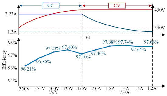
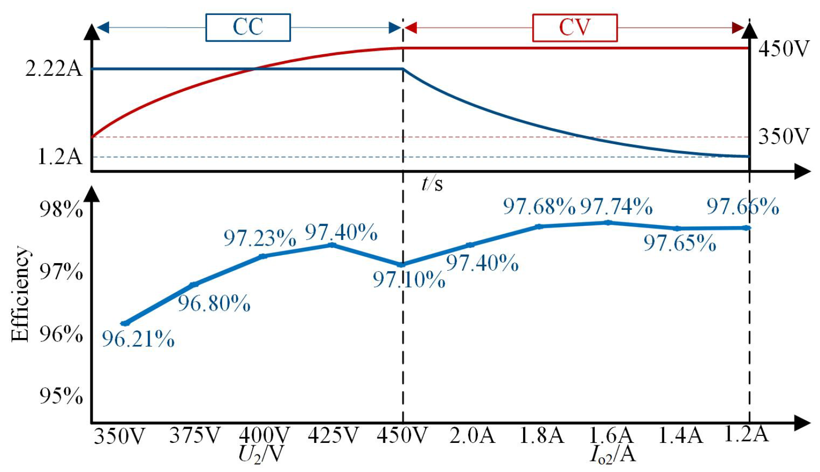
In forward mode, Figure 14 illustrates the power distribution between the main power circuit and the partial power regulation circuit of the converter. During the constant current phase, the secondary-side output voltage of the main power LLC-DCX circuit remains steady at 296 V, with the power being consistently 658 W. Because part of the power-regulating circuit transmits much less power than the main power circuit, the converter can always maintain high efficiency when regulating in the gain range. At this juncture, the main power circuit operates at the resonant frequency in open-loop mode, thereby achieving optimal efficiency. The output voltage regulation of the converter is mainly carried out by the partial power regulation circuit. This circuit dynamically adjusts the duty cycles of switches and in the Buck circuit according to the load size, simulating the constant-current–constant-voltage charging process of the battery. The efficiency curve of the converter is depicted in Figure 15. The overall efficiency of the converter exceeds 96%, with peak efficiency reaching up to 97.74%.
Figure 14.
The distribution of power in the forward mode.
Figure 15.
Constant-current–constant-voltage charging efficiency curve in forward mode.
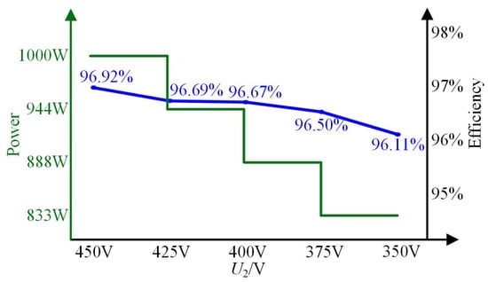
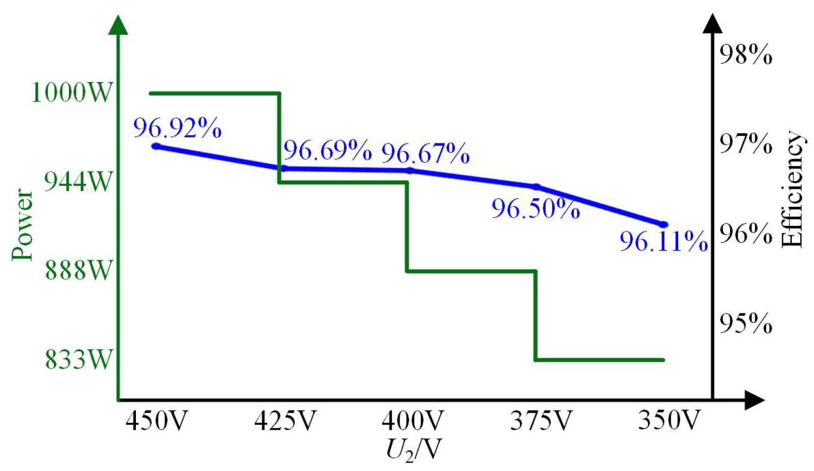
In backward mode, the power distribution relationship between the main power circuit and partial power-regulating circuit of the converter is shown in Figure 16. Since the voltage and power distribution relationship is the same as in the forward mode, the explanation is not repeated. In this mode, varying levels of output power are attainable by modulating the secondary-side input voltage. The battery discharge process is simulated through adjustments to the duty cycle of the switch and in the synchronous Buck converter, as well as by varying the size of the primary-side load. The efficiency curve is presented in Figure 17. The converter maintains an overall efficiency above 96.1%, with a peak efficiency of 96.92%.
Figure 16.
Power distribution in the backward mode.
Figure 17.
Efficiency graph of the converter during backward operation.
The voltage gain of the Buck circuit is proportional to the on-duty cycle d of the switching . In this paper, the duty cycle adjustment range of switch is 0.287–0.8, which has the potential to be further expanded. As the range of duty cycle adjustment is expanded, the voltage gain range will correspondingly widen. This allows the converter to adapt flexibly to varying voltage gain requirements while sustaining high efficiency.
6. Conclusions
This paper investigates a bidirectional resonant converter topology that utilizes partial power processing. It is characterized by a two-stage design, consisting of an LLC-DCX circuit in the front stage and a synchronous Buck voltage regulation circuit in the rear stage. The main power circuit operates in an open-loop state at the resonant frequency to maximize the performance benefits of the LLC resonant converter. A partial power regulation circuit, which handles a portion of the total power, controls the output voltage of the proposed converter by adjusting the duty cycle. The article presents an analysis of the voltage gain characteristics, power partitioning, and parameter design. A 1 kW prototype has been developed, featuring a constant primary voltage of 400 V and a variable secondary voltage ranging from 350 V to 450 V. The prototype has been tested to validate the proposed topology, achieving a peak forward efficiency of 97.74% and a peak backward efficiency of 96.92%. The converter is capable of further extending its regulatory range to meet diverse voltage gain requirements while maintaining high efficiency.
Author Contributions
Conceptualization, Q.Z. and J.L.; methodology, Z.W.; software, Z.W.; validation, Q.Z., J.L. and Z.W.; formal analysis, Q.Z.; investigation, J.L.; resources, Q.Z.; data curation, Z.W.; writing—original draft preparation, Z.W.; writing—review and editing, Q.Z.; visualization, J.L.; supervision, Q.Z.; project administration, Q.Z.; funding acquisition, Q.Z. All authors have read and agreed to the published version of the manuscript.
Funding
This research was funded by the Natural Science Foundation of Hebei under Grant E2023203148.
Data Availability Statement
The original contributions presented in this study are included in the article. Further inquiries can be directed to the corresponding author.
Conflicts of Interest
The authors declare no conflicts of interest.
References
- Ye, D.; Martinez, S. A Three-Port DC-DC Converter with Partial Power Regulation for a Photovoltaic Generator Integrated with Energy Storage. Electronics 2024, 13, 2304. [Google Scholar] [CrossRef] [Scilit]
- Li, X.; He, Y.; Li, M. Control Strategy for Bus Voltage in a Wind–Solar DC Microgrid Incorporating Energy Storage. Electronics 2024, 13, 5018. [Google Scholar] [CrossRef] [Scilit]
- Kim, K.M. Three-Level Double LLC Resonant Converter with Ripple-Free Input Current for DC Microgrid Application. Electronics 2024, 13, 4299. [Google Scholar] [CrossRef] [Scilit]
- Jin, K.; Ruan, X. Hybrid full-bridge three-level LLC resonant converter—A novel DC–DC converter suitable for fuel-cell power system. IEEE Trans. Ind. Electron. 2006, 53, 1492–1503. [Google Scholar] [CrossRef] [Scilit]
- Demirel, I.; Erkmen, B. A very low-profile dual output LLC resonant converter for LCD/LED TV applications. IEEE Trans. Power Electron. 2013, 29, 3514–3524. [Google Scholar] [CrossRef] [Scilit]
- Jin, T.; Xiao, X.S.; Zhang, Z.; Wu, W.; Yuan, Y.; Mao, X. Hybrid Control for Three-Level LLC Resonant Converter of Dual-Bridge for Wide Output Range. IEEE Trans. Power Electron. 2023, 38, 8612–8623. [Google Scholar] [CrossRef] [Scilit]
- Hu, Z.; Wang, L.; Wang, H.; Liu, Y.F.; Sen, P.C. An accurate design algorithm for LLC resonant converters—Part I. IEEE Trans. Power Electron. 2015, 31, 5435–5447. [Google Scholar] [CrossRef] [Scilit]
- Wei, Y.; Luo, Q.; Du, X.; Altin, N.; Alonso, J.M.; Mantooth, H.A. Analysis and design of the LLC resonant converter with variable inductor control based on time-domain analysis. IEEE Trans. Ind. Electron. 2019, 67, 5432–5443. [Google Scholar] [CrossRef] [Scilit]
- Mumtahina, U.; Wolfs, P.J. Multimode optimization of the phase-shifted LLC series resonant converter. IEEE Trans. Power Electron. 2018, 33, 10478–10489. [Google Scholar] [CrossRef] [Scilit]
- Khan, S.; Sha, D.; Jia, X.; Wang, S. Resonant LLC DC–DC converter employing fixed switching frequency based on dual-transformer with wide input-voltage range. IEEE Trans. Power Electron. 2020, 36, 607–616. [Google Scholar] [CrossRef] [Scilit]
- Guo, T.; Jia, P.; Zhang, X.; Zhang, Y.; Zhu, X. Analysis of the time-domain model of the LLC series resonant converter with frequency and single phase shifted control. IET Power Electron. 2024, 17, 1216–1234. [Google Scholar] [CrossRef] [Scilit]
- Tang, X.; Xing, Y.; Wu, H.; Zhao, J. An improved LLC resonant converter with reconfigurable hybrid voltage multiplier and PWM-plus-PFM hybrid control for wide output range applications. IEEE Trans. Power Electron. 2019, 35, 185–197. [Google Scholar] [CrossRef] [Scilit]
- Wei, Y.; Zhang, S.; Liu, J.; Mantooth, H.A. Hybrid PFM and PWM Modulation Strategy for Stacked Structure LLC Resonant Converter with Wide Input Voltage Range Application. IEEE Trans. Ind. Appl. 2024, 60, 4038–4053. [Google Scholar] [CrossRef] [Scilit]
- Shen, Q.; Sun, Q.; Chu, E.; Sun, C. Model Based Switching Frequency Secondary-Side Phase Shift Angle Matching for Optimizing Efficiency of PV Microconverter. IEEE Trans. Power Electron. 2024, 40, 3636–3656. [Google Scholar] [CrossRef] [Scilit]
- Zhou, K.; Liu, Y.; Wu, X. Research on Wide Input Voltage LLC Resonant Converter and Compound Control Strategy. Electronics 2022, 11, 3379. [Google Scholar] [CrossRef] [Scilit]
- Zuo, Y.; Shen, X.; Martinez, W. Reconfigurable LLC Resonant Converter for Wide Voltage Range and Reduced Voltage Stress in DC-Connected EV Charging Stations. IEEE Trans. Power Electron. 2025, 40, 3838–3843. [Google Scholar] [CrossRef] [Scilit]
- Zhao, Q.; Zhang, J.; Gao, Y.; Wang, D.; Yang, Q. Hybrid variable frequency LLC resonant converter with wide output voltage range. IEEE Trans. Power Electron. 2023, 38, 11038–11049. [Google Scholar] [CrossRef] [Scilit]
- Alaql, F.; Alfraidi, W.; Alhatlani, A.; Al-Shamma’a, A.A.; Hussein Farh, H.M.; Allehyani, A. A Detailed Analysis and Gain Derivation of Reconfigurable Voltage Rectifier-Based LLC Converter. Electronics 2024, 13, 3788. [Google Scholar] [CrossRef] [Scilit]
- Zhang, H.; Nie, J.; Sun, X.; Deng, Y.; Shu, Z. A Dual-Transformer-Based LLC Resonant Converter with Ultrawide Output Voltage Range. IEEE Trans. Power Electron. 2024, 40, 2457–2471. [Google Scholar] [CrossRef] [Scilit]
- Kim, M.; Jeong, H.; Han, B.; Choi, S. New parallel loaded resonant converter with wide output voltage range. IEEE Trans. Power Electron. 2017, 33, 3106–3114. [Google Scholar] [CrossRef] [Scilit]
- Wu, X.; Li, R.; Cai, X. Modified LLC resonant converter with LC antiresonant circuit in parallel branch for wide voltage range application. IEEE Trans. Power Electron. 2021, 37, 7387–7399. [Google Scholar] [CrossRef] [Scilit]
- Teng, J.H.; Chen, S.S.; Chou, Z.X.; Liu, B.H. Novel half-bridge LLC resonant converter with variable resonant inductor. IEEE Trans. Ind. Appl. 2023, 59, 6952–6962. [Google Scholar] [CrossRef] [Scilit]
- Liu, T.; Wu, X.; Yang, S. 1 MHz 48–12 V Regulated DCX with Single Transformer. IEEE J. Emerg. Sel. Topics Power Electron. 2021, 9, 38–47. [Google Scholar] [CrossRef] [Scilit]
- Neumayr, D.; Vöhringer, M.; Chrysogelos, N.; Deboy, G.; Kolar, J.W. P3 DCT—Partial-Power Pre-Regulated DC Transformer. IEEE Trans. Power Electron. 2019, 34, 6036–6047. [Google Scholar] [CrossRef] [Scilit]
- Liu, Y.C.; Chen, C.; Chen, K.D.; Syu, Y.L.; Dung, N.A. High-frequency and high-efficiency isolated two-stage bidirectional DC–DC converter for residential energy storage systems. IEEE J. Emerg. Sel. Top. Power Electron. 2019, 8, 1994–2006. [Google Scholar] [CrossRef] [Scilit]
- Jin, F.; Nabih, A.; Chen, C.; Chen, X.; Li, Q.; Lee, F.C. A high efficiency high density dc/dc converter for battery charger applications. In Proceedings of the 2021 IEEE Applied Power Electronics Conference and Exposition (APEC), Phoenix, AZ, USA, 14–17 June 2021; Volume 8, pp. 1994–2006. [Google Scholar]
- Liu, Q.; Qian, Q.; Ren, B.; Xu, S.; Sun, W.; Yang, L. A two-stage buck–boost integrated llc converter with extended zvs range and reduced conduction loss for high-frequency and high-efficiency applications. IEEE J. Emerg. Sel. Top. Power Electron. 2019, 9, 727–743. [Google Scholar] [CrossRef] [Scilit]
- Lu, Z.; Su, M.; Xu, G.; Li, L.; Liu, Y.; Chen, X. Integrated quasi-two-stage buck-lc converter with wide voltage gain range. IEEE Trans. Power Electron. 2024, 39, 9827–9838. [Google Scholar] [CrossRef] [Scilit]
- Ahmed, M.H.; Fei, C.; Lee, F.C.; Li, Q. Singlestage high-efficiency 48/1 v sigma converter with integrated magnetics. IEEE Trans. Ind. Electron. 2019, 67, 192–202. [Google Scholar] [CrossRef] [Scilit]
- Wei, R.; Ding, L.; Li, Y. Efficiency-oriented optimized design and control of hybrid fsbb-cllc converters with partial power processing capability. IEEE Trans. Power Electron. 2024, 39, 6364–6375. [Google Scholar] [CrossRef] [Scilit]
- Uno, M.; Oyama, R.; Sugiyama, K. Partially isolated single-magnetic multiport converter based on integration of series-resonant converter and bidirectional PWM converter. IEEE Trans. Power Electron. 2018, 33, 9575–9587. [Google Scholar] [CrossRef] [Scilit]
- Xu, Y.; Dai, X.; Zhang, Z.; Kang, Z.; Jin, T. A novel phase-shift pulsewidth modulation method for lightload bidirectional resonant converter. IEEE Trans. Power Electron. 2022, 38, 3257–3267. [Google Scholar] [CrossRef] [Scilit]
- Malan, W.L.; Vilathgamuwa, D.M.; Walker, G.R. Modeling and control of a resonant dual active bridge with a tuned cllc network. IEEE Trans. Power Electron. 2015, 31, 7297–7310. [Google Scholar] [CrossRef] [Scilit]
- Lee, B.-K.; Kim, J.-P.; Kim, S.-G.; Lee, J.-Y. An isolated/bidirectional pwm resonant converter for v2g (h) ev on-board charger. IEEE Trans. Veh. Technol. 2017, 66, 7741–7750. [Google Scholar] [CrossRef] [Scilit]
- Wei, Y.; Luo, Q.; Mantooth, H.A. Synchronous rectification for LLC resonant converter: An overview. IEEE Trans. Power Electron. 2021, 37, 3691–3696. [Google Scholar] [CrossRef] [Scilit]
- De Simone, S.; Adragna, C.; Spini, C.; Gattavari, G. Design-oriented steady-state analysis of LLC resonant converters based on FHA. In Proceedings of the International Symposium on Power Electronics, Electrical Drives, Automation and Motion, 2006. SPEEDAM 2006, Taormina, Italy, 23–26 May 2006; pp. 200–207. [Google Scholar]
- Jiang, C.; Liu, H. A Novel Interleaved Parallel Bidirectional Dual-Active-Bridge DC–DC Converter with Coupled Inductor for More-Electric Aircraft. IEEE Trans. Ind. Electron. 2021, 68, 1759–1768. [Google Scholar] [CrossRef] [Scilit]

Disclaimer/Publisher’s Note: The statements, opinions and data contained in all publications are solely those of the individual author(s) and contributor(s) and not of MDPI and/or the editor(s). MDPI and/or the editor(s) disclaim responsibility for any injury to people or property resulting from any ideas, methods, instructions or products referred to in the content. |
© 2025 by the authors. Licensee MDPI, Basel, Switzerland. This article is an open access article distributed under the terms and conditions of the Creative Commons Attribution (CC BY) license (https://creativecommons.org/licenses/by/4.0/).