Abstract
This work studies the impact of different physical and material parameters on the channel resistance, , and threshold voltage, , of nanowire field-effect transistors (NWFETs). In particular, by means of detailed numerical simulations, we investigate the role of the channel length, nanowire diameter, gate oxide thickness, channel-doping concentration, energy bandgap, oxide thickness, and gate oxide permittivity in a wide range of temperatures (200–500 K). Our findings show that optimal values for both 
		and 
		are achieved by reducing the nanowire channel length, as well as by increasing the nanowire diameter and doping concentration. Furthermore, NWFETs benefit from using wide-bandgap materials and thinner oxide layers with a higher permittivity. Notably, in short-channel NWFETs operating under ballistic transport, channel resistance remains nearly constant with temperature, governed by quantum conductance and injection statistics rather than temperature-sensitive scattering. These results underscore the complex interplay between material selection, doping levels, and device geometry in shaping the threshold voltage and the channel resistance of NWFETs. Also, they are useful for enhancing the device stability and advancing the design of NWFETs for the next-generation of nanoscale transistors.
    1. Introduction
Representing a significant development in semiconductor device structure, nanowire field-effect transistors (NWFETs) suggest one-dimensional nanowires as the channel material, replacing the planar systems defined in conventional metal-oxide-semiconductor field-effect transistors (MOSFETs). These devices are widely recognized as potential candidates for future electronics, offering improved electrostatic control, scalability, and compatibility with high-density integration.
The threshold voltage, , in NWFETs plays a crucial role in determining the device performance, power consumption, and overall reliability. It refers to the minimum gate voltage required to establish a conductive channel between the source and the drain terminals. Once the gate voltage surpasses , the transistor switches from the off state (non-conductive) to the on state (conductive), allowing the current to flow. A lower  can improve the switching speed, thus enabling faster operation in digital circuits. Several factors influence the threshold voltage in NWFETs, including the nanowire diameter, doping concentration, intrinsic carrier concentration, effective mass, temperature, energy bandgap, gate oxide permittivity, and oxide thickness. These parameters collectively determine the effective device behavior and stability, making the study of  crucial for optimizing the device’s performance.
Starting from previous results reported in the literature, we can state that increasing the nanowire diameter of silicon-based NWFETs causes a shift in the threshold voltage, with an improvement in the gate coupling []. Similarly, in silver-doped zinc-oxide NWFETs, the threshold voltage shifts to lower negative values as the nanowire diameter increases, although other electrical properties remain unchanged []. In cadmium selenide NWFETs, growth in the grain diameter through treatment affects the threshold voltage, suggesting that larger diameters improve electrical performance by minimizing defects and enhancing the electrical properties of the crystal [,]. For junctionless NWFETs, precise doping techniques allow for a tunable , making them ideal for specific applications. For example, in organic FETs, surface doping results in a positive shift of the threshold voltage [], while chemical doping in carbon nanotube FETs improves flexibility and the overall device performance []. Similarly, in silicon-doped hafnium-oxide ferroelectric FETs, accelerated doping modifies polarization, leading to an effective threshold voltage shift []. Moreover, a gate-all-around (GAA) design enhances the device performance by reducing the impact of random dopant fluctuations []. Finally, in SixGe1−x NWFETs, the tight-binding band structure reveals that the effective mass and the metal gate granularity significantly affect the device threshold voltage [,].
In a semiconductor device, the intrinsic carrier concentration, , increases with a rising temperature and, depending on the material bandgap, , more electrons can transition from the valence band to the conduction band. Devices based on materials with a lower , such as GaN and SiC, compared to silicon, exhibit a higher and more stable  due to a reduced number of thermally generated carriers. Also, they require more energy for electron transitions. Advances in nanostructuring have shown potential for controlling and enhancing a device’s stability []. For example, the use of NWFETs in bio-sensing applications enables the detection of DNA traces for precise intrinsic carrier concentration values [,].
As the temperature increases,  decreases because of a rising  and bandgap narrowing. For instance, in ZnO NWFETs, a temperature increase from 323 K to 363 K causes a significant  shift of −6.5 V, attributed to thermally activated electrons released from traps with an activation energy of 1.432 eV [,]. Studies reveal that material-specific effects, including phonon and surface scattering, reduce mobility and contribute to the  shifts [,]. In addition, in single-walled carbon nanotube FETs, the bandgap reduction enhances the carrier injection and reduces the short-channel effects, influencing  indirectly [,]. Also, in β-Ga2O3 nanobelts, with a wide bandgap of ~4.85 eV, high-energy proton irradiation causes a positive  shift, underscoring the bandgap’s role in determining the impact of external factors on the  [,]. Not only that, but the material choice also plays a key role. For instance, ozone treatment in ZnO NWFETs induces significant  shifts, demonstrating the influence of the oxide properties [].
The overall impact of the oxide capacitance on  varies across architectures and conditions, necessitating accurate exploration in diverse material systems. In fact, increasing the oxide thickness shifts the  by reducing the gate capacitance, requiring higher voltages to achieve the same electric field []. Conversely, thinner oxides improve the drive current, reduce leakage, and enhance switching speed and transconductance due to a better electrostatic control and mitigated short-channel effects [,]. Several studies reveal that oxide material properties influence  significantly [,,]. For example, indium oxide (In2O3) functionalized with Ag nanoparticles tunes  from −6.9 V to +7 V []. In zinc-oxide devices, gate-bias stress induces  instability due to charge trapping at the ZnO–dielectric interface, highlighting the effect of permittivity on charge dynamics [].
NWFETs exhibit a performance that is heavily influenced by factors such as the material composition and geometric parameters. These elements play a key role in shaping the channel resistance, which directly impacts the overall device performance. Silicon nanowires (SiNWs) have been the focus of extensive research due to their compatibility with established CMOS technology. Studies showed that SiNWs can help to reduce drain-induced barrier lowering (DIBL) and subthreshold swing (SS) compared to conventional MOSFETs, positioning them as an ideal choice for high-density integrated circuits []. Additionally, incorporating SiNWs in GAA configurations enhances the device performance by improving the gate control and minimizing the short-channel effects (SCEs) []. Germanium–tin (GeSn) nanowires have attracted interest for their high mobility and low effective mass, offering advantages for long-channel transistors. However, if transistor dimensions shrink below 10 nm, source-to-drain tunneling (SDT) emerges as a major limitation []. Silicon–germanium (SiGe) nanowires are also being investigated for their potential in tunnel field-effect transistors (TFETs). By utilizing low-bandgap SiGe in the source region, along with high-k dielectrics at the source–channel interface, the device performance significantly improves, making it a promising option for low-power applications. Simulations with different diameters and channel lengths reveal that smaller diameters enhance the band-to-band tunneling in weak conduction regimes, while larger diameters are more effective in strong conduction regimes [].
The channel length and diameter of NWFETs significantly affect device performance. To effectively reduce the SCEs and DIBL effects in the structure, shorter channel lengths and smaller diameters are preferred. Additionally, minimizing the diameter of SiNWs enhances the suppression of SCEs and improves electrostatic control. Also, physical parameters such as doping concentration and vacancy defects in SiNWs play crucial roles in shaping their band structure and transport characteristics [].
In our research, we explored the complex interplay of various factors that influence the threshold voltage and the channel resistance of NWFETs. Unlike previous studies that typically focused on one or two parameters, our study takes a broader approach. We discovered that shortening the nanowire channel lengths and increasing the doping concentrations significantly increase (in modulo) the threshold voltage by improving the gate control and boosting the carrier density. Also, we found that larger nanowire diameters further contribute to higher threshold voltages, as well as that employing higher oxide capacitances enables better gate modulations. At the same time, short-channel devices exhibit a lower resistance with an almost stable profile. Moreover, devices with higher doping concentrations exhibit lower resistance and reduced sensitivity to temperature. Finally, wide-bandgap materials lead to superior results and improve a device’s stability with temperature, thus making it well suited for high-power and high-temperature applications.
By investigating the combined impact of different technology parameters on two fundamental device figures of merit (i.e.,  and ), this study provides valuable insights for advancing the design of more reliable NWFETs.
2. Device Modeling
Figure 1 presents the geometric configuration of a cylindrical NWFET, which is similar to an MOSFET design. However, in the NWFET’s structure, a semiconductor nanowire replaces the conductive channel typically found in an MOSFET.
      
    
    Figure 1.
      The cylindrical gate-all-around nanowire field-effect transistor (NWFET) considered in this work.
  
In this unique device, an oxide layer is introduced as a dielectric separating the channel from the gate electrode. The nanowire is contacted at both ends by metal electrodes, designated as the source and drain regions. By applying a drain-to-source voltage, , and simultaneously varying the gate-to-source voltage, , an electric field is established to modulate the channel conductance. The resulting drain current, , was measured as a function of both  and  to provide insight into the device’s electrical behavior. The equivalent circuit of the device can be schematized as in Figure 2.
      
    
    Figure 2.
      NWFET equivalent circuit with series resistances.
  
The threshold voltage of an NWFET represents the minimum gate voltage required to induce a conductive inversion layer along the nanowire channel. This critical parameter is influenced by several device-specific and material-dependent factors, including the fixed positive charge on the gate electrode, dielectric permittivity of the nanowire material, flat-band voltage, gate oxide thickness, and channel-doping concentration. A recent analytical expression for the threshold voltage of an NWFET is in the form shown in the following []:


      where the intrinsic carrier concentration is modeled as follows:


By considering the cylindrical geometry of the gate oxide, the oxide capacitance per unit length () for a core–shell NWFET structure can be expressed as follows []:


      where  is the permittivity of the oxide,  is the radius of the nanowire channel,  is the oxide thickness,  is the vacuum permittivity, and  is the relative permittivity of the oxide.
For a nanowire semiconductor, the nanowire potential (calculated in volts) is given by the following:


      where  is the Boltzmann constant (1.38 × 10⁻²³ J/K),  is the absolute temperature is the elementary charge (1.602 × 10⁻¹⁹ C),  is the channel-doping concentration, and  is the intrinsic carrier concentration.
3. Contact Resistance in NWFETs
The metal–semiconductor contact is one of the main elements of a semiconductor device. Two types of metal–semiconductor contacts are known, namely, Schottky and ohmic contacts []. When a Schottky barrier (SB) is formed at an interface, the charge injection can be realized in the following two ways: thermionic emission and/or field emission (tunneling). On the other hand, ohmic contacts have linear and symmetrical I-V characteristics and a negligible contact resistance [].
To make high-performance devices, a good ohmic contact between the electrode and the semiconductor layer is required to inject the maximum current density across the contact. To create ohmic contacts, we can increase the semiconductor doping level or decrease the barrier height. Ohmic contacts also require electrodes with high and low work functions to inject holes and electrons, respectively, where the work function is the minimum energy required to remove an electron from the electrode’s Fermi level to the vacuum level []. Therefore, reducing the SB height when realizing ohmic contacts is essential to minimize the contact resistance and maximize the carrier injection efficiency, thus accurately improving the channel mobility, low-voltage driving, and high-frequency operation characteristics of devices. In conventional bulk NWFETs, the total resistance, , includes the following two components: series resistance, , and channel resistance, . The series resistance, , is an important factor for NWFETs. As the channel length scales down, the channel resistance becomes smaller and, therefore, it becomes more important to keep  much smaller than . In this context, the device’s total resistance, , can be calculated as the sum of  and .


Finally, the carrier mobility () is related to , as shown by the following equation []:


      where  is the channel length,  is the oxide capacitance per unit area,  is the gate voltage,  is the channel width, and  is the device threshold voltage.
4. Results and Discussion
In this section, we present a collection of simulation results focused on the influence of different technology parameters—channel length, doping concentration, semiconductor bandgap, nanowire radius, oxide thickness, and gate dielectric permittivity—in determining the NWFET threshold voltage and channel resistance. A summary of the device parameters used during the simulations is reported in Table 1 and Table 2.
       
    
    Table 1.
    Geometrical parameters used in the NWFET simulations.


    Table 2.
    Technological parameters used in the NWFET simulations.
  
4.1. Threshold Voltage Analysis
Considering a Si-based NWFET with a channel length of 20 nm, the temperature dependence of the threshold voltage is shown in Figure 3 for three different acceptor-doping concentrations. During the simulations, a metal work function of 5 eV was assumed. As we can see, for temperatures rising from 200 K to 400 K,  goes down, showing a temperature dependence due to the increase in the intrinsic carrier concentration. Higher doping levels determine a more negative  because of the enhanced built-in potential and the larger depletion region. This illustrates that dopant impurities and temperature both have a pronounced effect on the threshold voltage, as well as on the leakage currents and stability of the device.
      
    
    Figure 3.
      Threshold voltage versus temperature for three different acceptor-doping concentrations in a Si-based NWFET.
  
The impact of a shorter channel length on the  is shown in Figure 4. These curves were obtained for a silicon NWFET with a doping concentration of 1 × 1020 cm−3. The most negative  was observed for the shorter channel length (L = 5 nm), whereas the longer channel (L = 15 nm) had a relatively lower (in modulo) , which increases the subthreshold leakage and can be explained by stronger short-channel effects for small-scale devices that weaken the gate control over the channel.
      
    
    Figure 4.
      Threshold voltage versus temperature for three different channel length values.
  
Notably, Figure 5 shows that, for a rising temperature,  was reduced independently of the oxide thickness due to the increased internal carrier concentration, which reduces the gate voltage required for switching on the device. A thin oxide ( = 1 nm) results in a more negative  due to a higher gate capacitance and better electrostatic control of the channel. In contrast, a thick oxide can lead to weaker control by the gate. The obtained results emphasize the importance of increasing the electrostatic control by reducing the short-channel effects and reducing the oxide thickness to improve the NWFET’s performance.
      
    
    Figure 5.
      Threshold voltage versus temperature for three different oxide thicknesses.
  
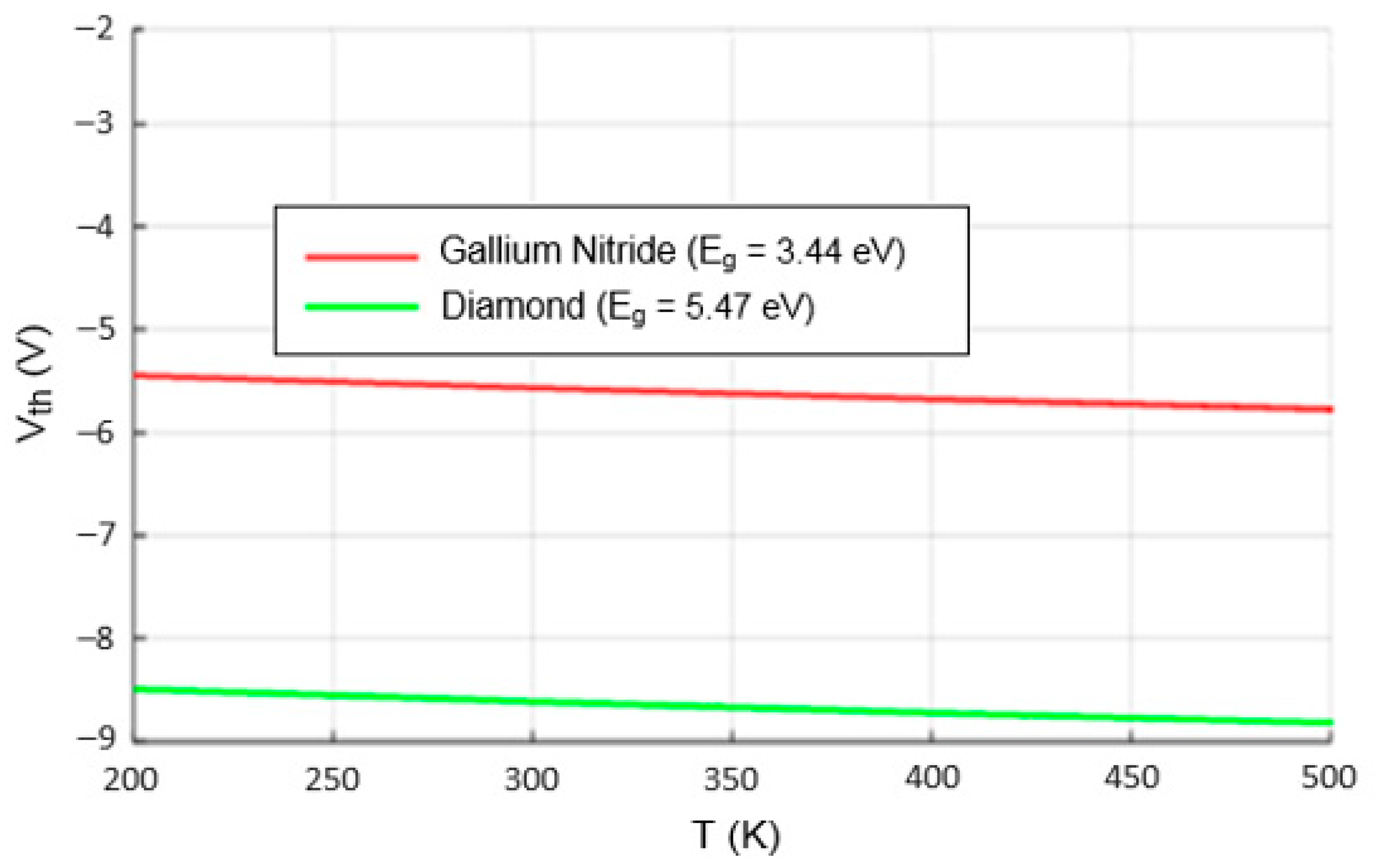
Figure 6 shows the ’s dependency on  for wide-bandgap materials, for example, gallium nitride (Eg = 3.44 eV) and diamond (Eg = 5.47 eV). As we can see, with a temperature variation from 200 K to 500 K,  decreased slightly. These behaviors can be attributed to thermal dependencies, such as the increasing intrinsic carrier concentration and the bandgap-narrowing effect, which indicate that semiconductors with larger bandgaps produce significantly fewer intrinsic carriers and, therefore, display a superior threshold voltage with an increased stability. Also, this result indicates that wide-bandgap semiconductors are less susceptible to leakage caused by temperature and are, thus, suitable for high-power and high-temperature applications.
      
    
    Figure 6.
      NWFET threshold voltage versus temperature for gallium nitride and diamond.
  
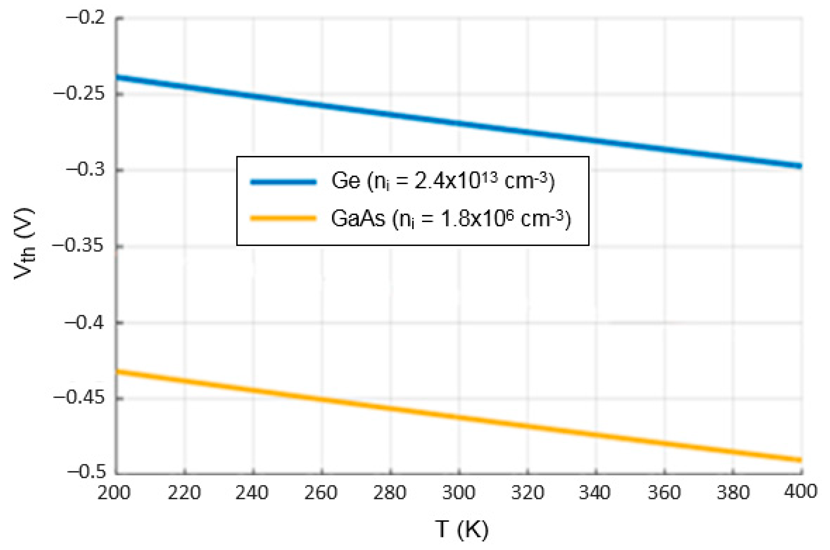
On the other hand, Figure 7 shows the variation in  with temperature for conventional semiconductors such as Ge (Eg = 0.66 eV) and GaAs (Eg = 1.43 eV). When compared with Si (Eg = 1.12 eV and  = 1.5 × 1010 cm−3), the Ge’s behavior is linked to the lower bandgap and the higher intrinsic carrier concentration, which reduce the built-in potential, thus resulting in a less negative . In fact, at T = 300 K, Ge has a higher  (2.4 × 1013 cm−3) than Si, which makes it intrinsically more conductive, leading to undesired leakage currents. Also, by considering the relative permittivity of materials (i.e., 11.7 for Si and 16 for Ge), we must also consider that the higher relative permittivity affects the gate capacitance of the nanowire as well. Similarly, the GaAs’s behavior is mainly determined by a relative permittivity of 12.9, although it presents an extremely low = 1.8 × 106 cm−3, which assures poor thermal generation of carriers.
      
    
    Figure 7.
      Threshold voltage versus temperature for germanium and gallium arsenide.
  
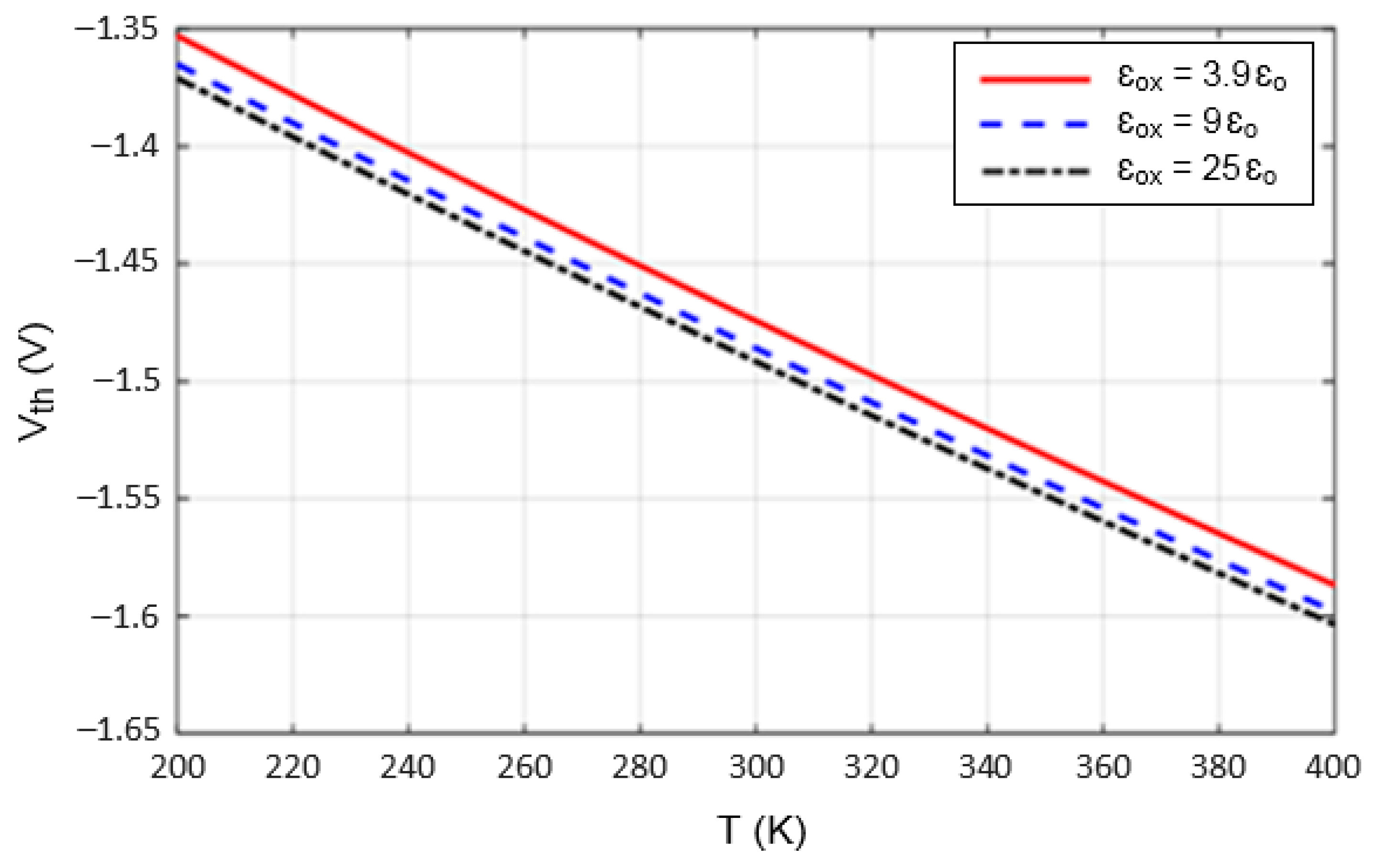
Figure 8 shows the variation in  for different values of the oxide permittivity, , which were 3.9, 9, and 25 relative to SiO2, Al2O3, and HfO2, respectively.
      
    
    Figure 8.
      Threshold voltage versus temperature for three different values of oxide permittivity.
  
As we can see,  appears to be only slightly dependent on this parameter, although when the temperature increases,  decreased for all cases as a consequence of the  increase and bandgap narrowing, which reduce the required gate voltage to turn on the device. However, a higher oxide permittivity tends to enhance the gate capacitance, leading to a slightly more negative value of .  
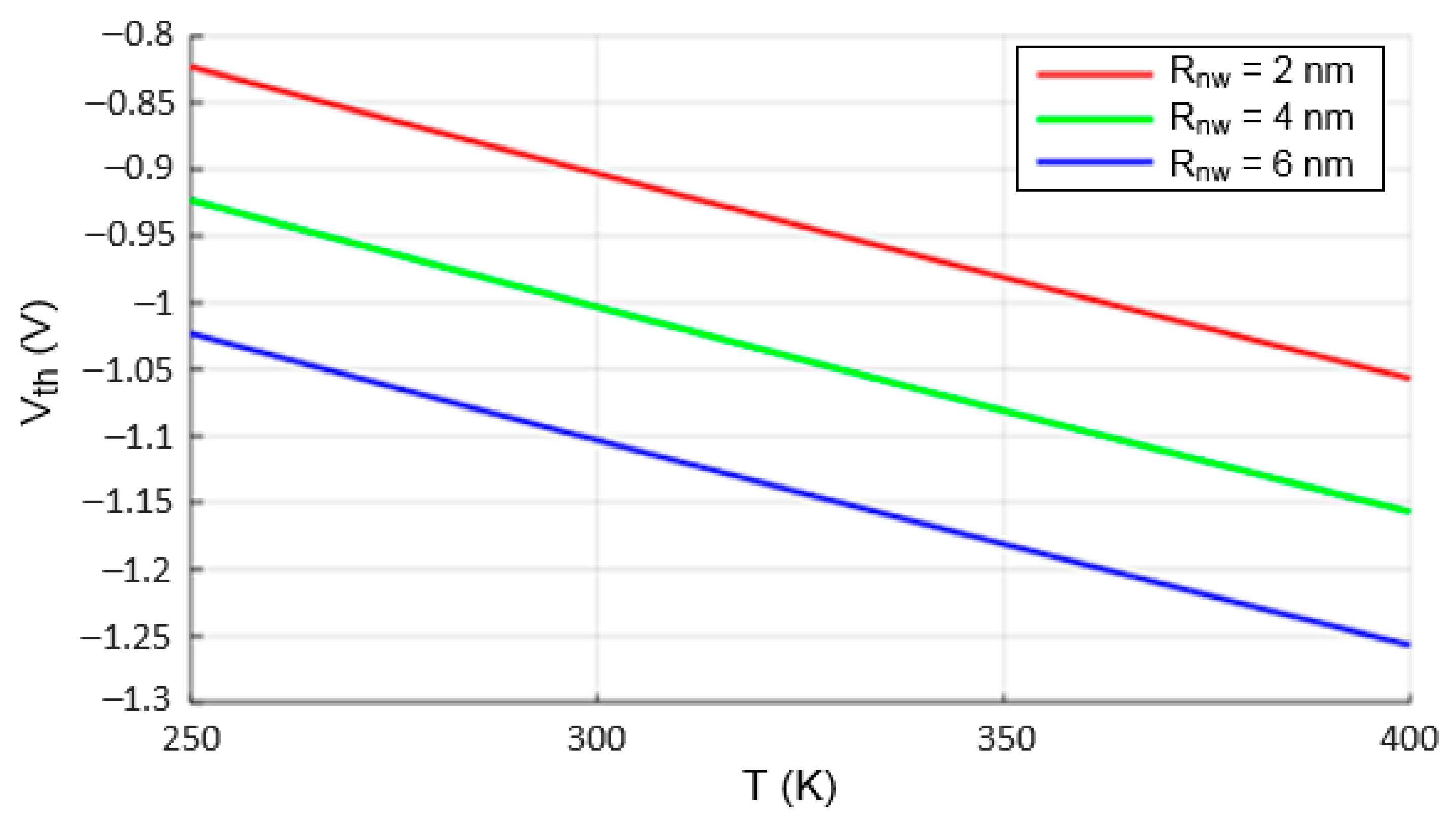
Finally, Figure 9 shows the variation in  with temperature for different values of the nanowire diameter. In particular, we considered  = 2 nm, 4 nm, and 6 nm. It is evident that small nanowires affect the gate control over the channel, determining a less negative , which can be attributed to changed quantum-confinement phenomena.
      
    
    Figure 9.
      Threshold voltage versus temperature for three different nanowire diameter values.
  
4.2. Channel Resistance Analysis
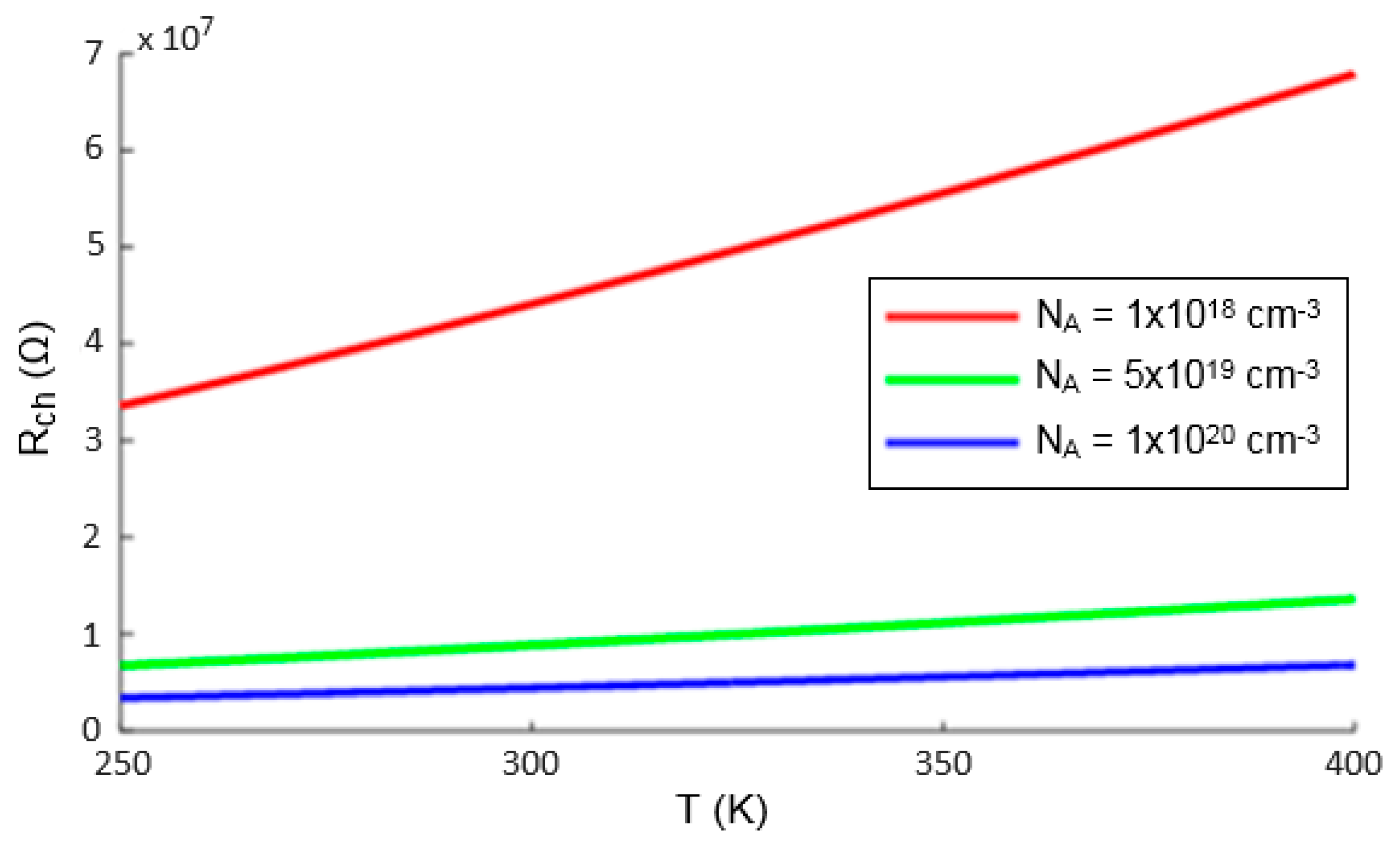
The channel resistance behaviors, as a function of temperature for different semiconductor doping levels, are shown in Figure 10. A carrier mobility reference value of µo = 100 cm2/Vs was assumed. As the temperature increased,  increased. This result is expected due to increased phonon scattering at higher temperatures, which reduces the carrier mobility. Also, the resistance was highest for the lowest doping level, and it decreased as the doping increased. Notably, we can state that higher doping concentrations not only reduce resistance, by increasing the carrier concentration, but also compensate for the mobility degradation due to the temperature. This appears to be a key finding for building effective NWFETs, particularly for applications involving high temperatures.
      
    
    Figure 10.
      Channel resistance versus temperature for different doping concentrations.
  
We know that phonon scattering increases in the channel with temperature. However, in semiconductor nanowires, especially at nanoscale dimensions, other effects like the enhanced carrier concentration due to thermal activation across the bandgap can counteract this. When these opposing effects manifest, carrier mobility reduction and carrier density increase cancel each other out, and the net change in the  value can be minimal. In this context, it is evident that optimizing the carrier mobility in the device structure is critical for reducing resistance and improving the NWFET current’s capabilities. In fact, as shown in Figure 11 for different carrier mobility reference values (NA = 5 × 1019 cm−3), while  increased with temperature due to enhanced phonon scattering, carrier mobilities that were too low led to a relevant increase in the device’s resistance ().
      
    
    Figure 11.
      Channel resistance versus temperature for different values of the carrier mobility.
  
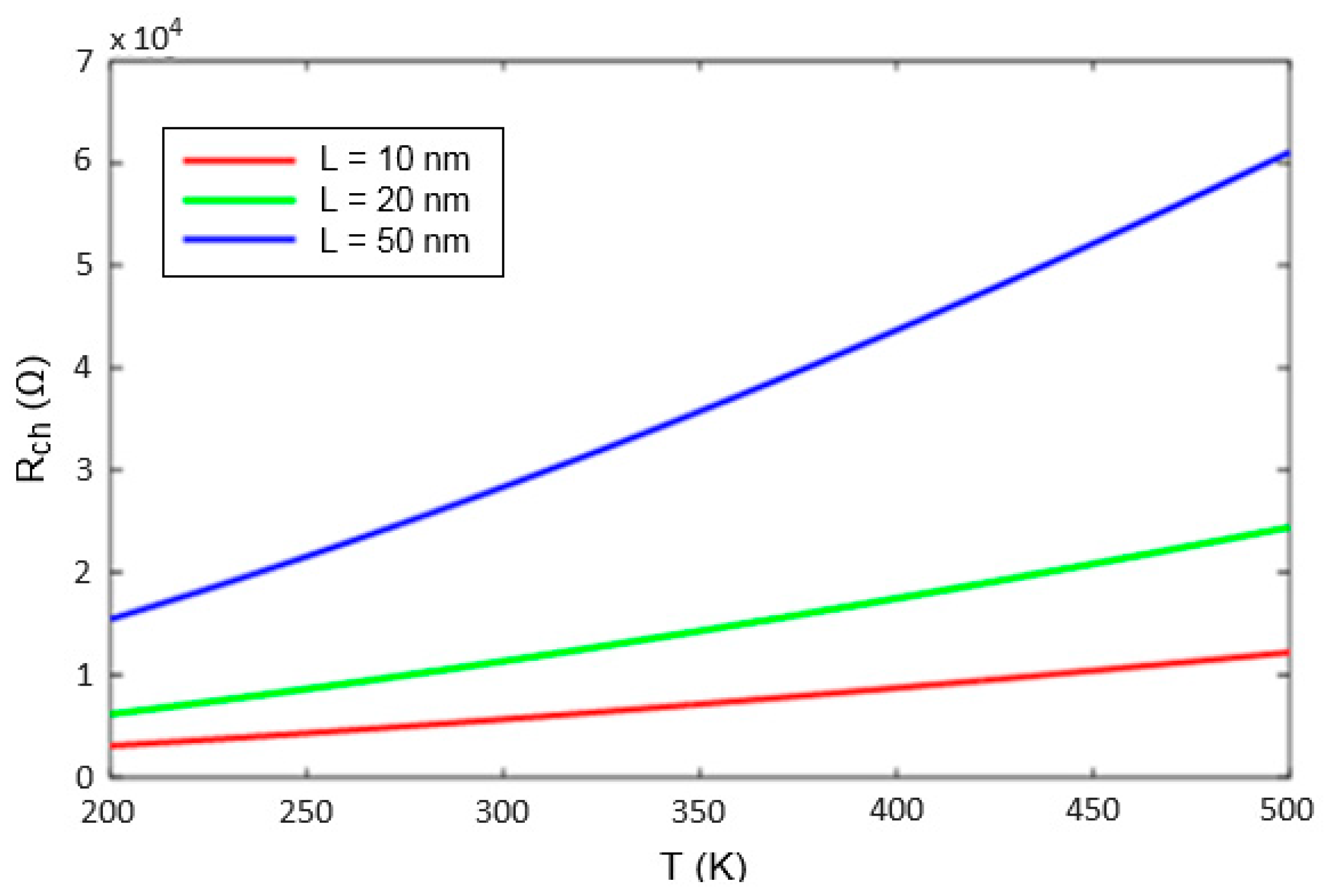
Similarly, Figure 12 shows the ’s dependence on T for different channel lengths (i.e., 10 nm, 20 nm, and 50 nm). Once again, the obtained results can be explained by the fact that charge carriers scatter more, increasing resistive losses. Also, shorter channel lengths perform better at higher temperatures. In fact, for L = 50 nm we can observe the steepest rise in , indicating that longer channel lengths intensify temperature sensitivity. On the other hand, when the channel length is very short, electron transport becomes fully ballistic, meaning that electrons travel through the channel with minimal scattering. Under such conditions, phonon scattering, which normally increases with temperature and leads to higher resistance in bulk or long-channel devices, plays a reduced role. In other words, since the channel length is short and the electrostatic control is strong, the mobility becomes less temperature dependent, leading to an almost stable  profile.
      
    
    Figure 12.
      Channel resistance versus temperature for different channel lengths.
  
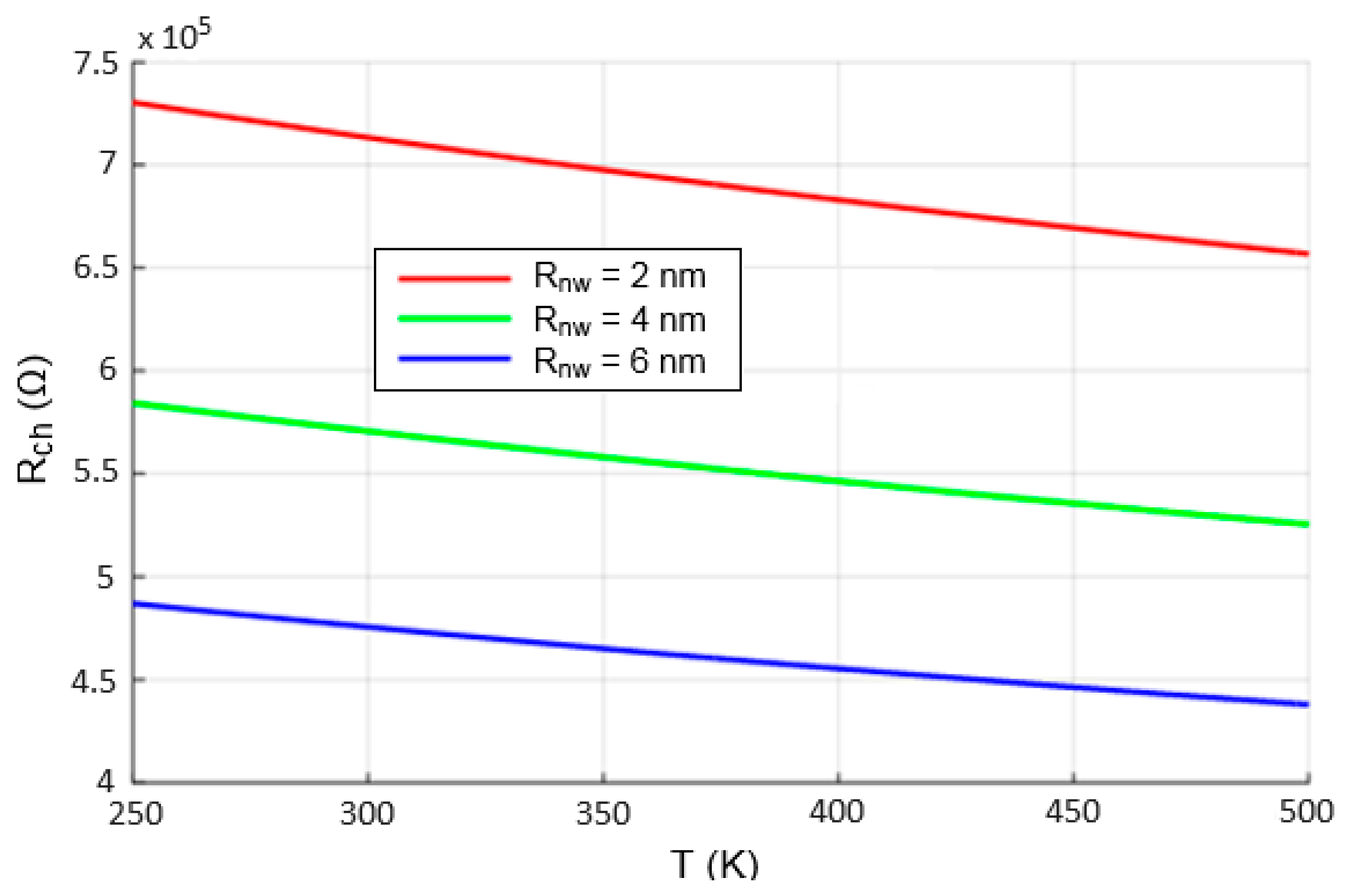
The effects of different nanowire diameters on the  curves are shown in Figure 13, where the channel resistance appears always slightly dependent on temperature. However, it is evident that a smaller nanowire radius exhibits a significantly higher resistance compared to the larger ones. This result is attributed to a stronger quantum confinement and an increased surface roughness scattering in narrower wires, which further impedes carrier transport.
      
    
    Figure 13.
      Channel resistance versus temperature for three different nanowire diameters.
  
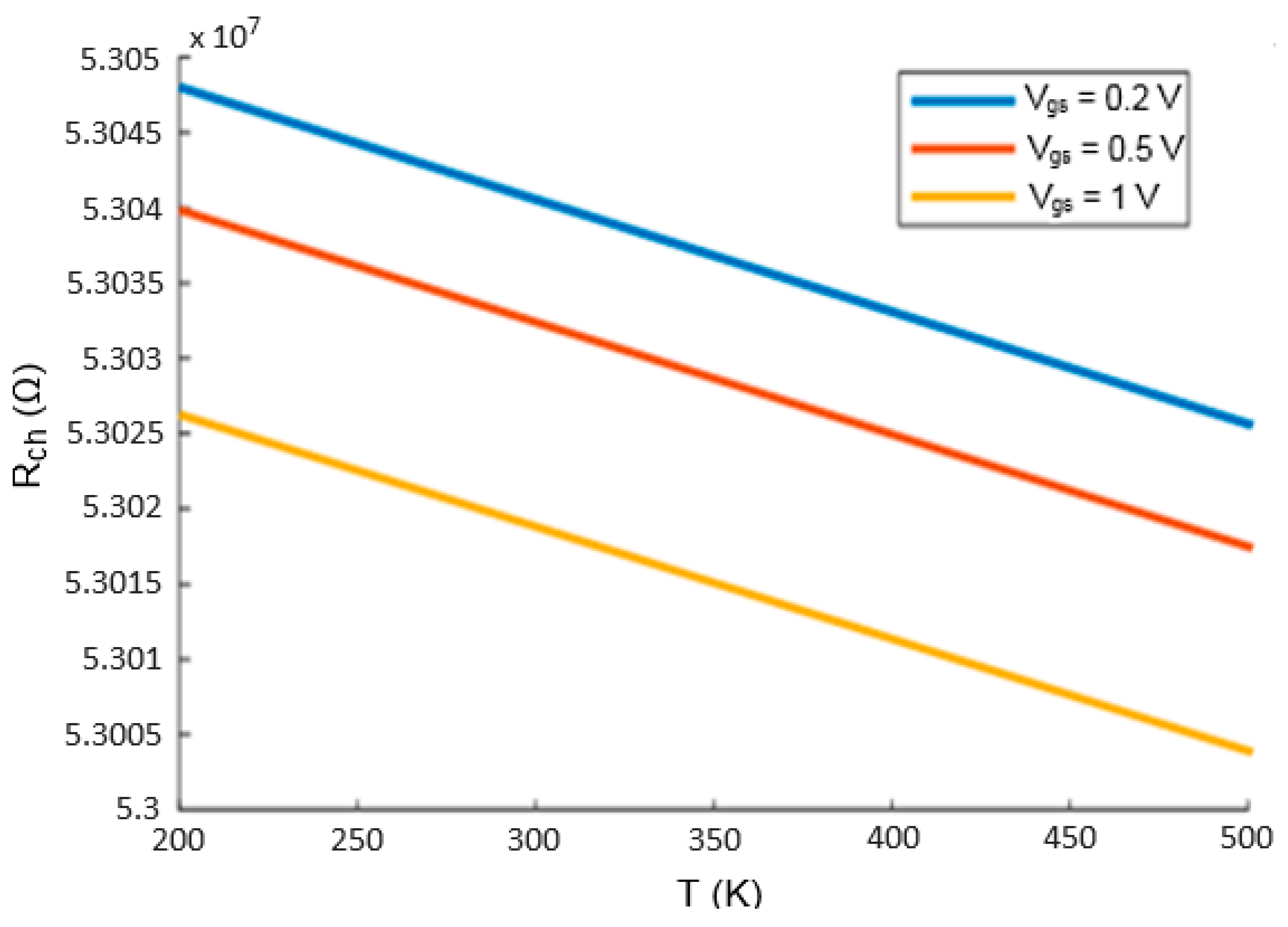
In the temperature analysis presented above, it is important to note that the NWFET’s channel resistance remained nearly constant with the gate-bias level, as shown in Figure 14.
      
    
    Figure 14.
      Channel resistance versus temperature for different values of Vgs.
  
This behavior reflects the dominance of the electrostatic control for managing gate modulation and short-channel effects efficiently. In fact, the extremely small variation across all curves emphasizes that the device operates in a regime where temperature has only minimal influence on resistance. In other words, the changes in lattice temperature have minimal influence on carrier dynamics, thus leading to an almost temperature-independent  over a given bias range, which is an ideal characteristic for stable nanoscale electronics.
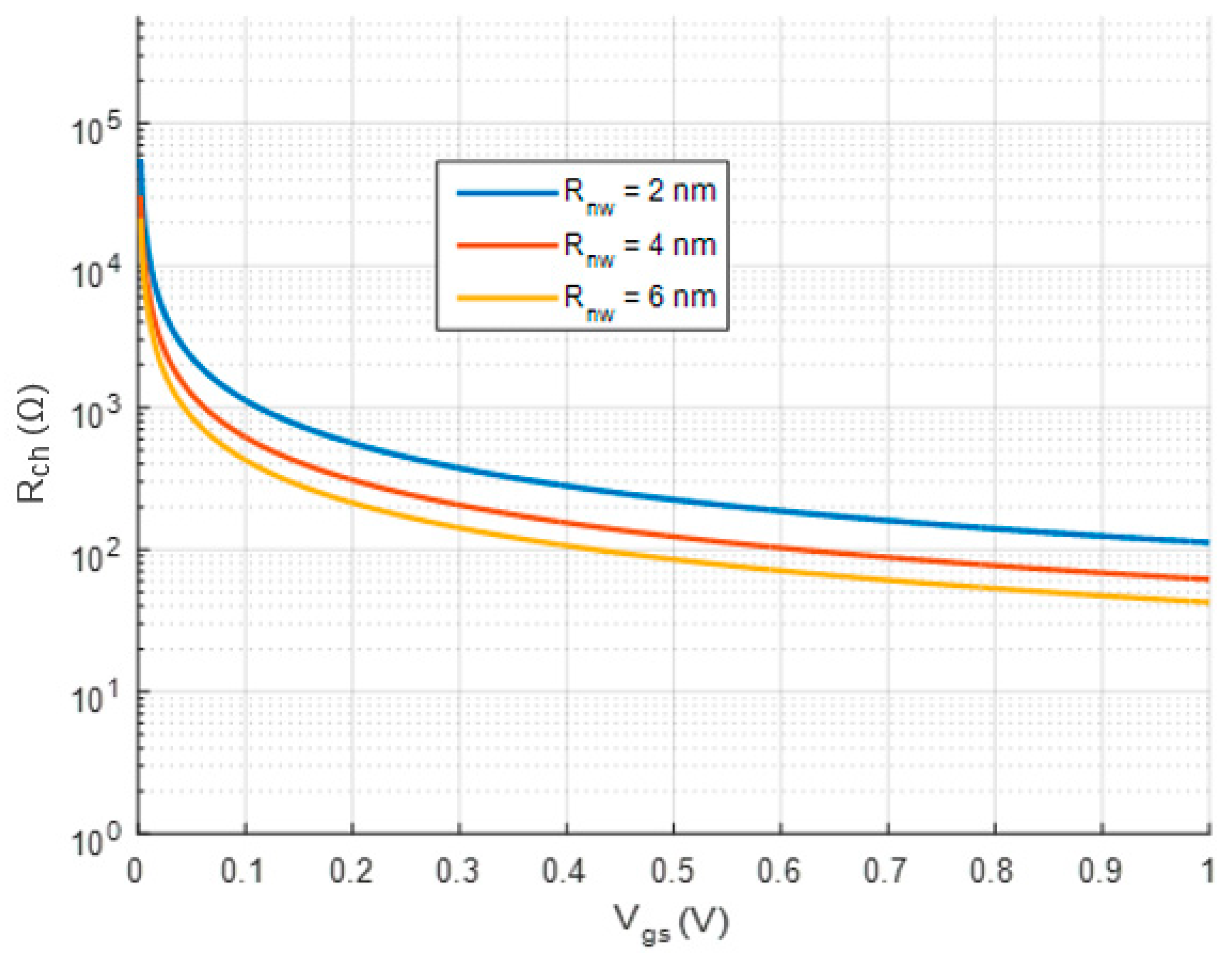
The dependence of the NWFET’s channel resistance on the gate-bias voltage, Vgs, for different design parameters, namely, the nanowire radius, channel length, and oxide thickness, is shown in detail in Figure 15, Figure 16 and Figure 17. From Figure 15, we can see that  decreased steeply as Vgs increased, indicating an enhanced electrostatic gating that induces a stronger inversion layer, thereby increasing the carrier density and lowering the resistance. In particular, from Figure 15, smaller nanowires exhibit a higher channel resistance due to a stronger quantum confinement, which limits the number of conducting subbands and suppresses the carrier mobility. In contrast, a wider nanowire (6 nm) benefits from reduced quantum effects and support higher carrier transport. This has a direct impact on the NWFET performance. In fact, devices with a larger radius offer lower resistance and a higher drive current, enhancing speed and transconductance, while a smaller radius, although better at controlling short-channel effects, suffer from a limited current drive and an increased delay due to the higher channel resistance.
      
    
    Figure 15.
      Channel resistance as a function of Vgs for different values of the nanowire radius.


    Figure 16.
      Channel resistance as a function of Vgs for different values of the channel length.


    Figure 17.
      Channel resistance as a function of Vgs for different values of the oxide thickness.
  
Similarly, from Figure 16, as Vgs increased the  value decreased across all lengths due to an enhanced carrier accumulation in the channel, which reduces the resistive path. Notably, longer channel devices exhibit higher channel resistance due to the increased physical length through which carriers must travel, leading to greater scattering and resistive losses. Conversely, the shortest channel (5 nm) displays the lowest resistance, promoting better current conduction. From a performance standpoint, while shorter channels enable a higher drive current and faster switching due to a reduced , they also pose challenges such as worsened short-channel effects (SCEs) and possible leakage. Longer channels mitigate SCEs but at the cost of an increased resistance and degraded performance metrics like transconductance and switching speed. Thus, careful optimization of the channel length is essential for balancing electrostatic integrity and performance in NWFETs.
Finally, from Figure 17, the devices with thinner gate oxides consistently exhibited a lower  because a thinner oxide improves gate electrostatic control, enhancing the gate capacitance and enabling a more efficient inversion of the channel at lower voltages. In contrast, thicker oxides weaken the gate influence over the channel, requiring higher voltages to induce a comparable charge density, thus resulting in higher resistance values. A thinner tox is advantageous, as it reduces the , leading to higher drive currents, faster switching speeds, and improved transconductance. However, this comes with challenges such as an increased gate leakage and reliability concerns. Hence, optimizing oxide thickness is another key for balancing electrostatics, performance, and leakage in advanced NWFET designs.
4.3. Current–Voltage Characteristics
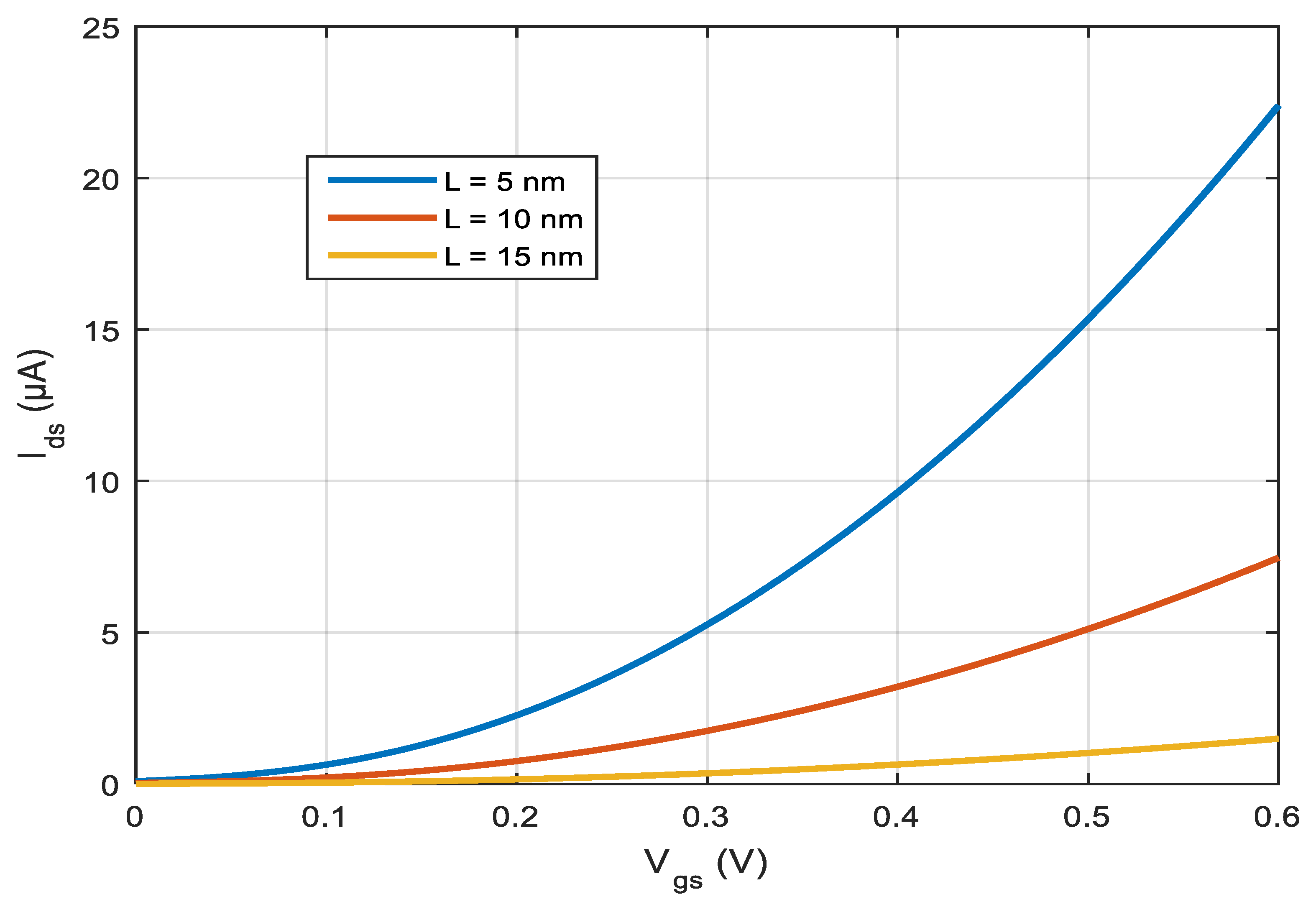
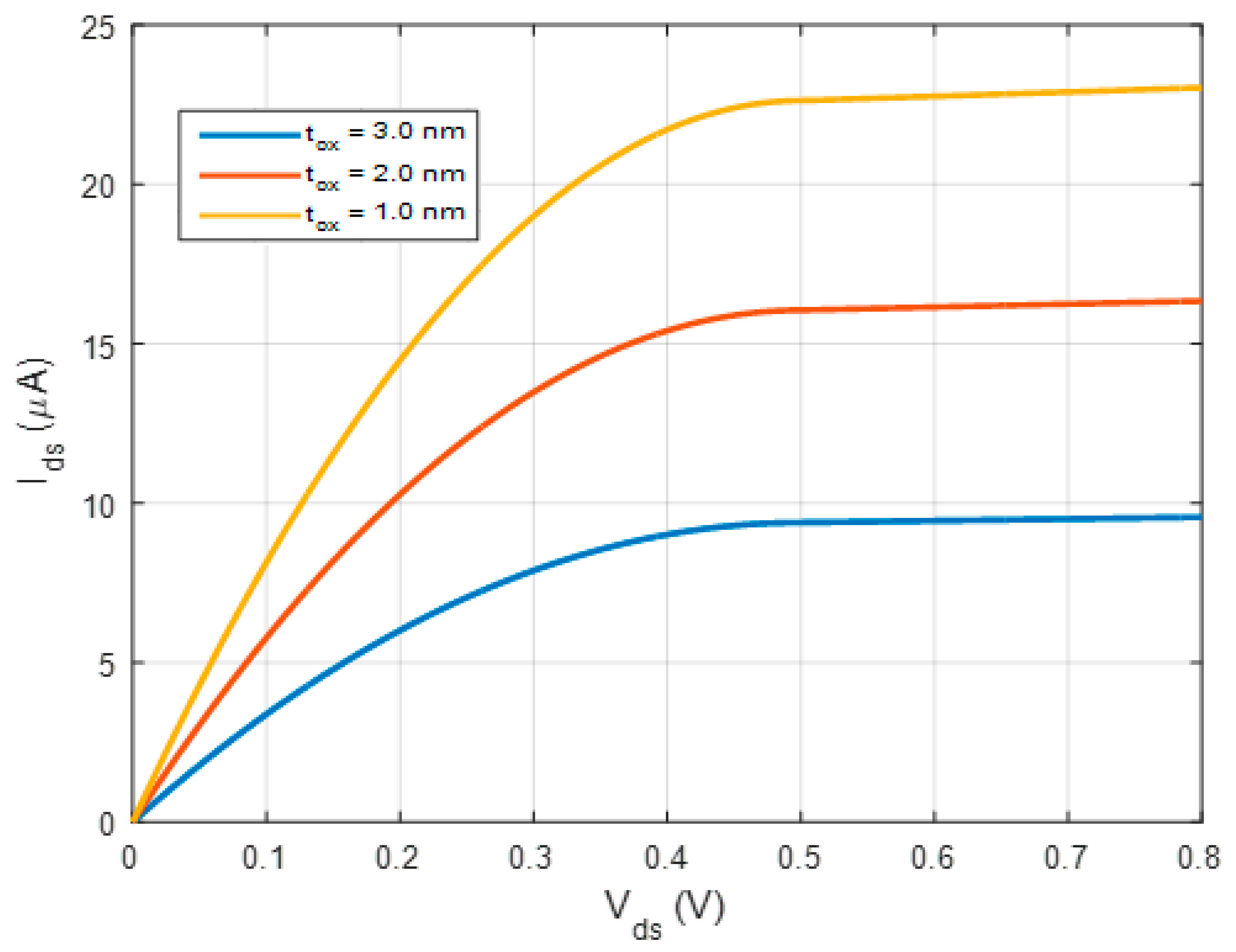
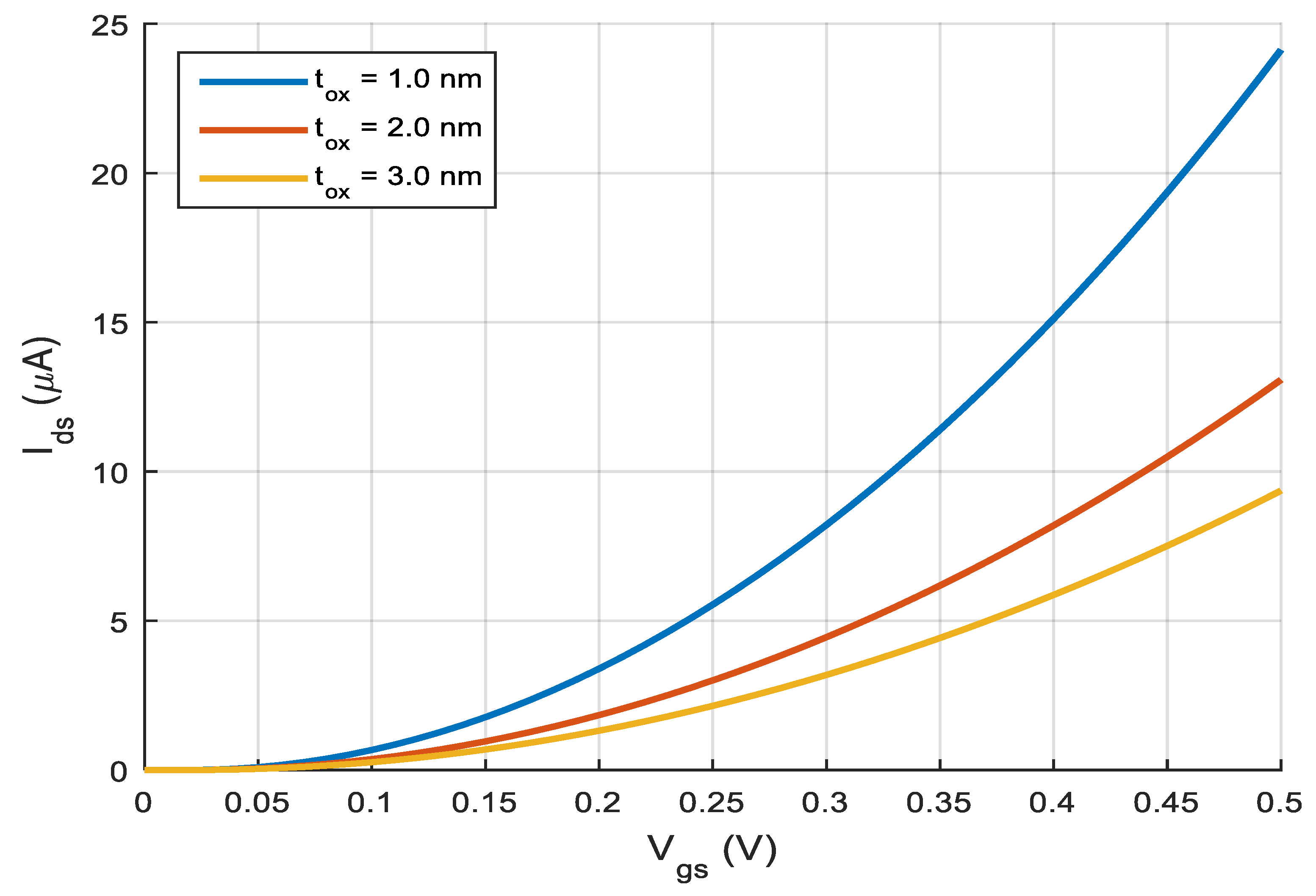
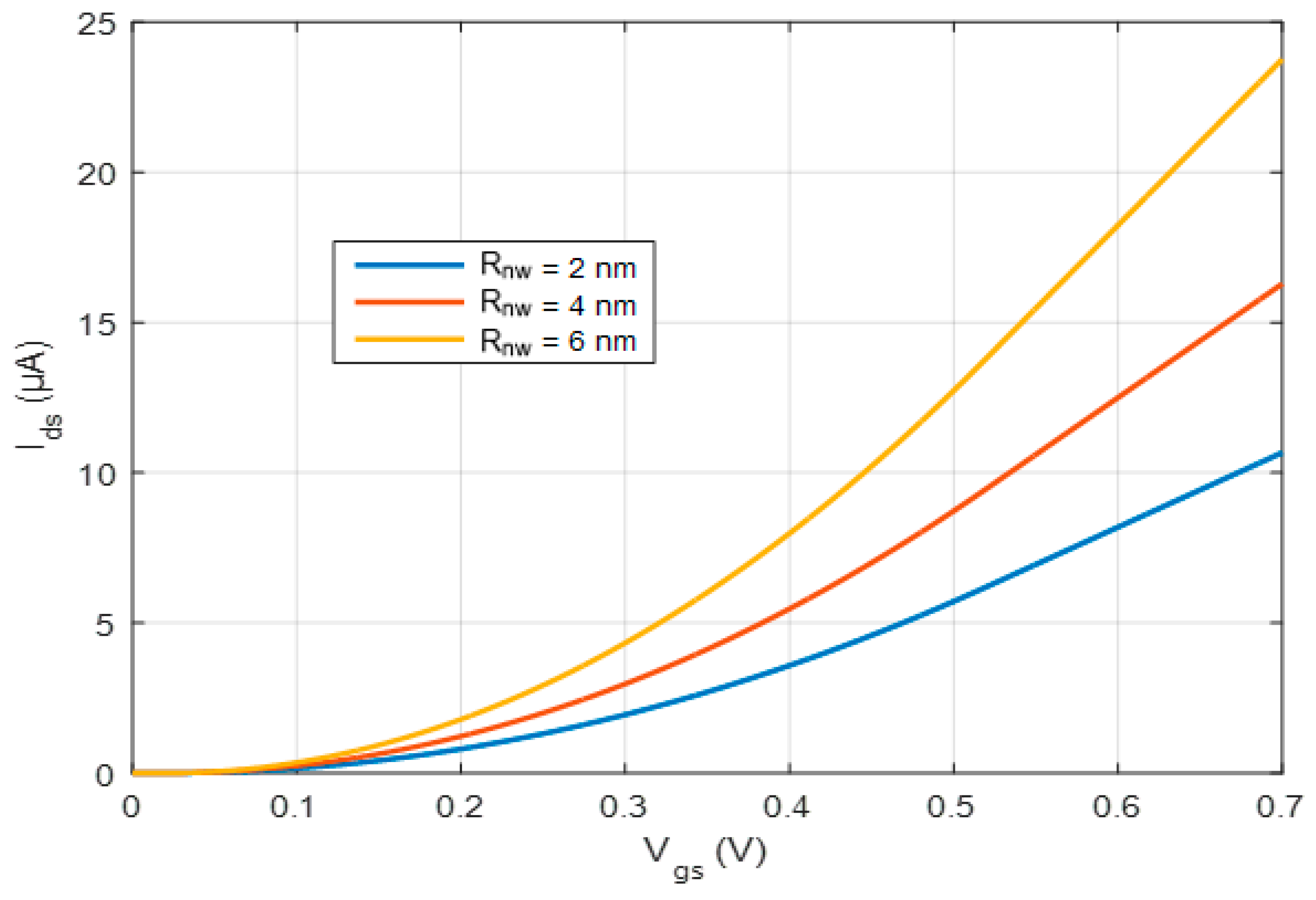
In this section, we present the NWFET’s output characteristics, namely, the drain-to-source current (Ids) versus the drain-to-source voltage (Vds), and the transfer characteristics, namely, the drain-to-source current (Ids) versus the gate-to-source voltage (Vgs), calculated for different geometrical device parameters (channel length, oxide thickness, and nanowire radius), as shown in Figure 18, Figure 19, Figure 20, Figure 21, Figure 22 and Figure 23.
      
    
    Figure 18.
      Ids–Vds curves for different values of the channel length. Vgs = 0.7 V.


    Figure 19.
      Ids–Vgs curves for different values of the channel length. Vds = 0.5 V.


    Figure 20.
      Ids–Vds curves for different values of the oxide thickness. Vgs = 0.6 V.


    Figure 21.
      Ids–Vgs curves for different values of the oxide thickness. Vds = 0.5 V.


    Figure 22.
      Ids–Vds curves for different values of the nanowire radius. Vgs = 0.7 V.


    Figure 23.
      Ids–Vgs curves for different values of the of the nanowire radius. Vds = 0.5 V.
  
The curves in Figure 18 indicate that shorter channel lengths result in significantly higher Ids values, especially in the saturation region due to a reduced channel resistance and an enhanced carrier injection efficiency. This behavior can be attributed to reduced scattering events and shorter transit times for carriers in shorter channels, which lead to an improved drive current. Moreover, the early onset of saturation in longer channels, combined with lower drain currents, highlights a stronger electrostatic control but at the cost of a reduced current capability. In contrast, the 5 nm channel shows higher current levels and a more gradual transition to saturation, which may also suggest the onset of short-channel effects such as DIBL. In addition, this plot emphasizes the performance versus control trade-off in ultra-scaled NWFETs and highlights once again the significance of a channel length optimization for balancing current drive and potential loss of gate control.
From Figure 19, we can clearly see that as the channel length decreased, the drain current significantly increased for a given gate voltage. This is a direct consequence of a reduced channel resistance and an improved carrier transport efficiency in shorter channels. At shorter lengths, carriers experience less scattering and shorter transit times, enabling a higher current flow. Moreover, the steeper subthreshold slope and rapid current increase in shorter channels suggest stronger gate control and higher transconductance. However, the increased Ids for L = 5 nm may also indicate the influence of short-channel effects, such as threshold voltage roll-off and DIBL, which become prominent as the electrostatic control of the gate weaken with an aggressive device scaling.
Figure 20 clearly shows the impact of the oxide scaling on the device performance. For a given Vds, transistors with thinner gate oxides yield higher drain currents, a result of the enhanced gate control over the channel and the stronger electrostatic coupling. As the oxide becomes thinner, the gate capacitance increased, leading to a higher inversion charge in the channel and, thus, a greater carrier injection from source to drain.
In Figure 20, each curve initially shows a linear increase in Ids with Vds, followed by the saturation regime as the channel near the drain enters pinch-off and velocity saturation effects dominate. The saturation current increases with a decrease in the oxide thickness, underlining the importance of aggressive oxide scaling in improving drive current and switching performance for high-performance NWFETs.
From Figure 21, we can see that decreasing the oxide thickness improved the gate control over the channel, leading to a higher drive current for a given Vgs. The thinnest oxide exhibited the highest Ids due to the stronger gate capacitance, enhancing the inversion layer and boosting carrier density. As tox increased, the gate lost efficiency in controlling the channel potential, causing a reduction in the output current.
Finally, Figure 22 and Figure 23 show the effect of a different nanowire radius. In particular, as Rnw increased, the drain current significantly increased for all investigated Vds (Figure 22). This behavior can be physically attributed to the enlarged cross-sectional area of the channel, which reduces the channel resistance and allows for more carriers to flow. A larger radius also accommodates a greater inversion charge due to the increased volume, enhancing the current drive. However, larger nanowire diameters can potentially degrade the electrostatic gate control, possibly due to a strong gate coupling or high-k dielectrics, as assumed in the simulations. All curves show typical transistor behavior with linear and saturation regions, and the saturation current increased with the radius.
At the same time, Figure 23 demonstrates how increasing the Rnw enhanced the device’s drive current capability. In fact, as the nanowire radius increased, the cross-sectional area available for carrier transport also increased, which reduced the quantum confinement and allowed for more charge carriers to flow through the channel for a given Vgs. This is reflected in the upward shift of the Ids curve as Rnw increased from 2 nm to 6 nm. Furthermore, the steeper slope in the subthreshold and moderate inversion regions for larger Rnw suggests an improved gate control and stronger channel formation, leading to a higher transconductance. These effects are consistent with enhanced electrostatics and reduced channel resistance in thicker nanowires, making them more favorable for high-performance applications.
5. Conclusions
This work offers an in-depth exploration of the roles of different physical and material parameters in determining two fundamental figures of merit of an NWFET, namely, the device’s threshold voltage and channel resistance. Reducing the channel doping or the nanowire diameter tends to worsen short-channel effects and weaken the gate control. These changes drive the threshold voltage down and the channel resistance up. The resistance variation is further amplified under thermal stress. On the other hand, by reducing the channel length and the gate oxide thickness, the electrostatic control of the channel is improved. This enhancement leads to a more favorable shift in both the threshold voltage and channel resistance behaviors. Also, semiconductors with a wide bandgap display a threshold voltage with an increased stability.
A key finding is that, for short-channel devices operating under a ballistic or quasi-ballistic regime, the channel resistance remains remarkably stable with temperature (200–500 K). This temperature insensitivity arises considering the resistance governed by quantum conductance, electrostatics, and injection statistics, which are weakly temperature dependent. Moreover, if the carrier transport is dominated by quantum-confinement effects or degenerately doped conditions, especially at nanoscale dimensions, the scattering mechanisms do not significantly affect the overall channel resistance. In fact, the carrier injection is not thermally activated and then the resistive behavior is mainly geometric, not thermal, leading once again to a channel resistance nearly invariant with temperature. Such behavior is particularly advantageous for devices operating under variable thermal conditions. The near-constant channel resistance with temperature and the observed current-voltage characteristics for different geometrical device parameters showed a hallmark of advanced nanoscale transistors. Notably, NWFETs appear to be compelling candidates for high-temperature-tolerant nanoelectronic systems and, in general, for the next-generation of transistors, as the industry continues to push for more compact and thermally robust semiconductor technologies.
Author Contributions
Conceptualization, R.M. and L.D.; methodology, R.M., L.D., K.Z., F.P., G.M. and F.G.D.C.; validation, L.D., K.Z. and F.P.; writing—original draft, R.M.; writing—review & editing, R.M. and F.P.; formal analysis, L.D., F.P., G.M. and F.G.D.C.; supervision, F.G.D.C. All authors have read and agreed to the published version of the manuscript.
Funding
This research received no external funding.
Data Availability Statement
The data presented in this study are available upon request from the corresponding author.
Conflicts of Interest
The authors declare no conflicts of interest.
References
- Lee, S.H.; Lee, T.I.; Lee, S.J.; Lee, S.M.; Yun, I.; Myoung, J.M. Electrical Characteristics of Metal Catalyst-Assisted Etched Rough Silicon Nanowire Depending on the Diameter Size. ACS Appl. Mater. Interfaces 2015, 7, 929–934. [Google Scholar] [CrossRef] [PubMed]
 - Kim, K.; Debnath, P.C.; Park, D.-H.; Kim, S.; Lee, S.Y. Controllability of Threshold Voltage in Ag-Doped ZnO Nanowire Field Effect Transistors by Adjusting the Diameter of Active Channel Nanowire. Appl. Phys. Lett. 2010, 96, 083103. [Google Scholar] [CrossRef]
 - Lee, S.; Yoon, J.-S.; Lee, J.; Jeong, J.; Yun, H.; Lim, J.; Lee, S.; Baek, R.-H. Novel Modeling Approach to Analyze Threshold Voltage Variability in Short Gate-Length (15–22 nm) Nanowire FETs with Various Channel Diameters. Nanomaterials 2022, 12, 1721. [Google Scholar] [CrossRef]
 - Ayvazian, T.; Xing, W.; Yan, W.; Penner, R.M. Field-Effect Transistors from Lithographically Patterned Cadmium Selenide Nanowire Arrays. ACS Appl. Mater. Interfaces 2012, 4, 4445–4452. [Google Scholar] [CrossRef] [PubMed]
 - Van, N.H.; Lee, J.-H.; Sohn, J.I.; Cha, S.N.; Whang, D.; Kim, J.M.; Kang, D.J. High Performance Si Nanowire Field-Effect-Transistors Based on a CMOS Inverter with Tunable Threshold Voltage. Nanoscale 2014, 6, 5479. [Google Scholar] [CrossRef]
 - Singh, P.; Miao, J.; Park, W.-T.; Kwong, D.-L. Minimum Detectable Strain Improvement in Junctionless Nanowire FET Sensors. In Proceedings of the 2012 IEEE 25th International Conference on Micro Electro Mechanical Systems (MEMS), Paris, France, 29 January–2 February 2012; pp. 1328–1331. [Google Scholar] [CrossRef]
 - Zessin, J.; Xu, Z.; Shin, N.; Hambsch, M.; Mannsfeld, S.C.B. Threshold Voltage Control in Organic Field-Effect Transistors by Surface Doping with a Fluorinated Alkylsilane. ACS Appl. Mater. Interfaces 2019, 11, 2177–2188. [Google Scholar] [CrossRef]
 - Zhang, H.; Liu, W.; Wu, P.; Guo, M.; Xu, X.; Xi, X.; Gao, J.; Rao, G.; Wang, S. Room Temperature Threshold Switching Behaviors of Bi0.9Nd0.1Fe1−xCoxO3 Nanoparticles. J. Mater. Chem. C 2015, 3, 4141–4147. [Google Scholar] [CrossRef]
 - Lee, J.; Badami, O.; Carrillo-Nuñez, H.; Berrada, S.; Medina-Bailon, C.; Dutta, T.; Adamu-Lema, F.; Georgiev, V.P.; Asenov, A. Variability Predictions for the Next Technology Generations of n-type SixGe1−x Nanowire MOSFETs. Micromachines 2018, 9, 643. [Google Scholar] [CrossRef]
 - Aldegunde, M.; Martinez, A.; Asenov, A. Non-equilibrium Green’s Function Analysis of Cross Section and Channel Length Dependence of Phonon Scattering and Its Impact on the Performance of Si Nanowire Field Effect Transistors. J. Appl. Phys. 2011, 110, 094518. [Google Scholar] [CrossRef]
 - Vardhan, P.H.; Mittal, S.; Ganguly, S.; Ganguly, U. Analytical Modeling of Metal Gate Granularity Based Threshold Voltage Variability in NWFET. Solid-State Electron. 2018, 147, 26–34. [Google Scholar] [CrossRef]
 - Nayak, K.; Agarwal, S.; Bajaj, M.; Oldiges, P.J.; Murali, K.V.R.M.; Ramgopal, V. Metal-Gate Granularity-Induced Threshold Voltage Variability and Mismatch in Si Gate-All-Around Nanowire n-MOSFETs. IEEE Trans. Electron Devices 2014, 61, 3892–3895. [Google Scholar] [CrossRef]
 - Wu, C.-C.; Ko, F.-H.; Yang, Y.-S.; Hsia, D.-L.; Lee, B.-S.; Su, T.-S. Label-Free Biosensing of a Gene Mutation Using a Silicon Nanowire Field-Effect Transistor. Biosens. Bioelectron. 2009, 25, 820–825. [Google Scholar] [CrossRef] [PubMed]
 - Kim, K.; Debnath, P.C.; Kim, S.; Lee, S.Y. Temperature Stress on Pristine ZnO Nanowire Field Effect Transistor. Appl. Phys. Lett. 2011, 98, 113109. [Google Scholar] [CrossRef]
 - Ghedira, S.; Fargi, A.; Besbes, K. Temperature Dependent Analytical Model for the Threshold Voltage of the SiC VJFET with a Lateral Asymmetric Channel. Electronics 2021, 10, 1494. [Google Scholar] [CrossRef]
 - Sakuna, N.; Muanghlua, R.; Niemcharoen, S.; Ruangphanit, A.; Poyai, A. Temperature and Devices Dimension Dependence on Threshold Voltage, the Low Field Mobility and the Series Parasitic Resistance of PMOSFET. In Proceedings of the 2013 10th International Conference on Electrical Engineering/Electronics, Computer, Telecommunications and Information Technology (ECTI-CON), Krabi, Thailand, 15–17 May 2013; pp. 1–6. [Google Scholar] [CrossRef]
 - Morioka, N.; Yoshioka, H.; Suda, J.; Kimoto, T. Quantum-Confinement Effect on Holes in Silicon Nanowires: Relationship between Wave Function and Band Structure. J. Appl. Phys. 2011, 109, 064318. [Google Scholar] [CrossRef]
 - Yang, G.; Jang, S.; Ren, F.; Pearton, S.J.; Kim, J. Influence of High-Energy Proton Irradiation on β-Ga2O3 Nanobelt Field-Effect Transistors. ACS Appl. Mater. Interfaces 2017, 9, 40471–40476. [Google Scholar] [CrossRef]
 - Minhaj, E.H.; Esha, S.R.; Adnan, M.M.R.; Dey, T. Impact of Channel Length Reduction and Doping Variation on Multigate FinFETs. In Proceedings of the 2018 International Conference on Advancement in Electrical and Electronic Engineering (ICAEEE), Gazipur, Bangladesh, 22–24 November 2018; pp. 1–4. [Google Scholar] [CrossRef]
 - Awadhiya, B.; Kondekar, P.N.; Yadav, S.; Upadhyay, P. Insight into Threshold Voltage and Drain Induced Barrier Lowering in Negative Capacitance Field Effect Transistor. Trans. Electr. Electron. Mater. 2021, 22, 267–273. [Google Scholar] [CrossRef]
 - Choe, M.; Park, W.; Kang, J.-W.; Jeong, S.; Hong, W.-K.; Lee, B.H.; Park, S.-J.; Lee, T. Investigation of Threshold Voltage Instability Induced by Gate Bias Stress in ZnO Nanowire Field Effect Transistors. Nanotechnology 2012, 23, 485201. [Google Scholar] [CrossRef]
 - Fan, J.-C.; Lee, S.-F. Giant Magnetoresistance Effect in Ni-Fe-Mo Alloys. MATEC Web Conf. 2016, 67, 02023. [Google Scholar] [CrossRef]
 - Price, A.; Martinez, A. Impact of Oxide Thickness on the Performance of a GaAs NWFET. J. Phys. Conf. Ser. 2015, 609, 012004. [Google Scholar] [CrossRef]
 - Jamwal, D.; Dass, D.; Prasher, R.; Vaid, R. Impact of Scaling Gate Oxide Thickness on the Performance of Silicon Based Triple Gate Rectangular NWFET. In Physics of Semiconductor Devices; Springer: Cham, Switzerland, 2014; pp. 581–584. [Google Scholar] [CrossRef]
 - Wu, L.; Xu, J.; Li, Q.; Fan, Z.; Mei, F.; Zhou, Y.; Yan, J.; Chen, Y. Enhanced Performance of In2O3 Nanowire Field Effect Transistors with Controllable Surface Functionalization of Ag Nanoparticles. Nanotechnology 2020, 31, 355703. [Google Scholar] [CrossRef] [PubMed]
 - Vardhan, P.H.; Ganguly, S.; Ganguly, U. An Accurate Expression to Estimate the Metal Gate Granularity Induced Threshold Voltage Variability in NWFETs. Solid-State Electron. 2019, 152, 65–71. [Google Scholar] [CrossRef]
 - Dobrescu, D.; Cretu, B.; Simoen, E.; Veloso, A.; Voicu-Spineanu, A.; Dobrescu, L. Si GAA NW FETs Threshold Voltage Evaluation. Solid-State Electron. 2022, 194, 108317. [Google Scholar] [CrossRef]
 - Bahador, S.N.; Tan, M.L.P.; Ismail, R. Performance Evaluation of Silicon Nanowire Gate-All-Around Field-Effect Transistors and Their Dependence of Channel Length and Diameter. Sci. Adv. Mater. 2015, 7, 190–198. [Google Scholar] [CrossRef]
 - Bahador, N.; Tan, M.L.P.; Ahmadi, M.T.; Ismail, R. A Unified Drain–Current Model of Silicon Nanowire Field-Effect Transistor (SiNWFET) for Performance Metric Evaluation. Sci. Adv. Mater. 2014, 6, 354–360. [Google Scholar] [CrossRef]
 - Yadav, D.; Nair, D.R. Performance Evaluation of Germanium-Tin Nanowire PFETs: Impact of Mole Fraction, Orientation and Doping. In Proceedings of the 2018 4th IEEE International Conference on Emerging Electronics (ICEE), Bengaluru, India, 17–19 December 2018; pp. 1–4. [Google Scholar] [CrossRef]
 - Patel, J.; Suman, P.; Lemtur, A.; Sharma, D. Performance Booster Electrical Drain SiGe Nanowire TFET (EDD-SiGe-NW-TFET) with DC Analysis and Optimization. In Information and Communication Technology for Intelligent Systems; Smart Innovation, Systems and Technologies; Springer: Singapore, 2019; pp. 567–574. [Google Scholar] [CrossRef]
 - Irfan, M.; Sattar, A.; Iqbal, A.; Khan, M.F.; Amjad, R.J.; Mahmood, H.; Latif, H.; Akbar, N.; Alvi, F.; Sultana, I. Investigation of Effects of Diameter, Doping and Vacancy Defects on the Band Structure and Transport Properties of Silicon Nanowires for Potential Applications in Field-Effect Transistors. J. Electron. Mater. 2019, 48, 2761–2769. [Google Scholar] [CrossRef]
 - Chaujar, R.; Yirak, M.G. Sensitivity Investigation of Junctionless Gate-All-Around Silicon Nanowire Field-Effect Transistor-Based Hydrogen Gas Sensor. Silicon 2023, 15, 609–621. [Google Scholar] [CrossRef]
 - Zhou, X.; Waldron, N.; Boccardi, G.; Sebaai, F.; Merckling, C.; Eneman, G.; Sioncke, S.; Nyns, L.; Opdebeeck, A.; Maes, J.W.; et al. Scalability of InGaAs Gate-All-Around FET Integrated on 300 mm Si Platform: Demonstration of Channel Width down to 7 nm and Lg down to 36 nm. In Proceedings of the 2016 IEEE Symposium on VLSI Technology, Honolulu, HI, USA, 14–16 June 2016; pp. 1–2. [Google Scholar] [CrossRef]
 - Blank, T.V.; Gol’dberg, Y.A. Mechanisms of current flow in metal-semiconductor ohmic contacts. Semiconductors 2007, 41, 1263–1292. [Google Scholar] [CrossRef]
 - Lin, J.C.; Yu, S.Y.; Mohney, S.E. Characterization of Low-Resistance Ohmic Contacts to n- and p-Type InGaAs. J. Appl. Phys. 2013, 114, 044504. [Google Scholar] [CrossRef]
 - Jo, G.; Maeng, J.; Kim, T.-W.; Hong, W.-K.; Choi, B.-S.; Lee, T. Channel-Length and Gate-Bias Dependence of Contact Resistance and Mobility for In2O3 Nanowire Field Effect Transistors. J. Appl. Phys. 2007, 102, 084508. [Google Scholar] [CrossRef]
 
Disclaimer/Publisher’s Note: The statements, opinions and data contained in all publications are solely those of the individual author(s) and contributor(s) and not of MDPI and/or the editor(s). MDPI and/or the editor(s) disclaim responsibility for any injury to people or property resulting from any ideas, methods, instructions or products referred to in the content.  | 
© 2025 by the authors. Licensee MDPI, Basel, Switzerland. This article is an open access article distributed under the terms and conditions of the Creative Commons Attribution (CC BY) license (https://creativecommons.org/licenses/by/4.0/).