Abstract
This paper presents the design and implementation of a D-band CMOS phase shifter based on a parallel reflective-load topology. Two phase-shifting architectures are explored, namely a 360° continuously tunable phase shifter and a 180° phase shifter combined with a phase inverter, enabling full 360° phase coverage. The circuit was simplified, and the number of bias lines was minimized to facilitate future array circuit implementation. In addition, a serial peripheral interface (SPI) circuit is implemented to simplify bias control and reduce the number of external connections during array chip packaging.
1. Introduction
Using higher carrier frequencies for wireless communication is becoming increasingly important for achieving high capacity and low latency. The wide bandwidth at these frequencies is ideal for ultra-fast data transmission, which is crucial for applications such as fixed wireless access and front/backhaul systems, both in urban and rural areas [1]. Research has focused on frequencies below 100 GHz, but due to certain limitations, the D-band is emerging as the new promising frequency range, aided by advances in measurement equipment and hardware technology. There is ongoing research into beamforming systems that use carrier frequencies up to the D-band, focusing on improving both efficiency and performance [2]. Extensive research has been conducted on the development of circuits for D-band beamforming, with the ultimate objective of implementing these circuits in array configurations and integrating them through advanced packaging techniques.
Although most CMOS-based designs have traditionally targeted frequencies below 100 GHz due to limited transistor fT and fmax, the D-band (110–170 GHz) offers significantly wider bandwidth for next-generation wireless links. However, circuit implementation at these frequencies becomes increasingly challenging because of higher conductor losses, varactor quality degradation, and parasitic coupling. Despite these inherent CMOS loss limitations, we have successfully developed a novel circuit design technique to realize a high-performance phase shifter that effectively mitigates the high-frequency challenges.
One of the simplest approaches to implement phase shifting is using transmission delay lines. A 5-bit differential phase shifter employing a transmission delay line was demonstrated in [3], which utilized eight lumped-element cells and operated in the 120~146 GHz frequency range. Similarly, a 3-bit phase shifter based on an SPDT switch, coupler and filter network has also been presented [4]. Delay-line-based designs offer bi-directional operation and low DC power consumption. However, they suffer from significant insertion loss, lack of analog control capability, and substantial chip area overhead as the number of bits increases.
To address these limitations, a trombone-like structure has been proposed, where propagation distance is controlled through two parallel transmission lines periodically interconnected via a switch network [5]. While this technique provides improved chip area and flexibility in delay tuning, it still does not enable true analog phase control and requires many switches, which significantly increases the complexity of DC biasing.
The vector-sum phase shifter topology has recently emerged as one of the most widely adopted approaches for high-frequency phase shifting. In this architecture, variable-gain amplifiers are used to control the gain states, while careful device sizing and biasing enable precise phase control. Compact vector-sum phase shifters implemented in BiCMOS technology and operating at D-band and higher frequencies have been presented [6,7]. Additionally, at 60 GHz, techniques have been proposed to minimize impedance variations resulting from phase and gain tuning, thereby reducing phase and gain errors [8]. Despite these advantages, vector-sum phase shifters inherently require many transistors, leading to increased DC power consumption and a heigh biasing complexity. Without a dedicated serial peripheral interface (SPI), controlling these bias states becomes impractical, and the large number of control lines also complicates system packaging.
Achieving a wide phase-shifting range using RTPS topology at high frequencies is one of the primary challenges in phase shifter design. Conventional approaches to extend the phase range often rely on cascading multiple phase-shifter stages or incorporating phase inverters. For instance, a 250-nm InP HBT implementation demonstrated a full 360° phase shift using two cascaded RTPS stages [9], while designs in 90-nm SiGe BiCMOS and 0.12-μm SiGe process employed two cascaded stages combined with a one-bit phase inverter [10,11]. Although effective, these methods increase chip area, insertion loss, and DC power consumption, making them less suitable for compact and energy-efficient systems.
This work presents a reflection-type phase shifter architecture that achieves continuous 360° phase control using a single phase-shifter core. A passive phase inverter is utilized to minimize DC power consumption and reduce bias-line complexity, while a parallel reflective-load technique is introduced to extend the phase control range. The proposed approach enables a compact, low-loss, and power-efficient solution for D-band phase shifter integration.
2. Proposed Phase Shifter Overview Configuration
In this study, two versions of phase shifters were designed using parallel load termination which is shown in Figure 1.
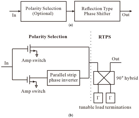
Figure 1.
Block diagram of the proposed phase shifter: (a) overall architecture and (b) detailed configuration.
The first approach, which enables a full 360° phase shift, utilizes only a Lange coupler and a load termination without polarity selection, thereby minimizing chip area while providing a wide phase-shifting range. Additionally, this circuit requires only a single bias line, allowing for bias control without an SPI (Serial Peripheral Interface) circuit in a packaged implementation, which simplifies the overall design.
The second approach, which provides a 180° phase shift, consists of a two-way divider, a switch amplifier, a phase inverter, a two-way combiner, a Lange coupler, and a load termination. Compared with the first approach, this configuration achieves stable 180° phase shifting even with variations in the designed inductance values and offers low loss characteristics. In this architecture, the two-way divider and switch amplifier select the desired phase of the signal, either 0° or 180°, which is then fed into the Lange coupler and subsequently phase-shifted by the load termination. Since two control signals are applied to the switch, an N-channel array implementation would require 2N bias lines. To overcome this limitation, SPI (Serial Peripheral Interface) control is adopted for biasing, while the varactor bias is applied manually.
3. Design of Circuit Elements
3.1. Tunable Load Termination
To achieve a wide and continuous phase-shifting capability in D-band phase shifters, various load termination topologies were investigated. Conventional designs are limited by the intrinsic quality factor of the varactor and its relatively small capacitance tuning ratio (Cmax/Cmin), which makes big insertion losses and loss variation caused by impedance change fundamentally restrict the achievable phase-shifting range and in high-frequency applications.
A simple capacitive-load topology, where a single varactor serves as a load termination, provides only about 40° of phase tuning range, rendering it unsuitable for 360° phase shifting. The LC reflective-load topology improves the range slightly by adding a series inductor in front of the varactor; however, its phase-shifting capability rapidly degrades at higher frequencies, and its performance is highly sensitive to inaccuracies in the inductance and capacitance modeling, often resulting in instability.
The CLC-π reflective-load topology, which is widely used in phase shifters, achieves a marginally larger tuning range than the LC topology. Independent control of each varactor within the CLC-π structure can further extend the range, but this requires additional bias lines and significantly increases design complexity, making it less attractive for compact, high-frequency integration.
To overcome these limitations, a parallel LC reflective-load topology was adopted, as shown in Figure 2. This structure employs two LC load terminations connected in parallel with intentionally different inductance values. The inductors are realized using high-impedance transmission lines, allowing precise inductance control and ensuring stable high-frequency operation. By carefully selecting the inductance difference, a trade-off between gain and tuning range is established: A small inductance difference yields a wide tuning range exceeding 360° but results in relatively lower gain, and a larger inductance difference achieves higher gain at the cost of a reduced tuning range of approximately 180°. This approach provides flexibility to optimize phase shifter performance depending on the target system requirements.
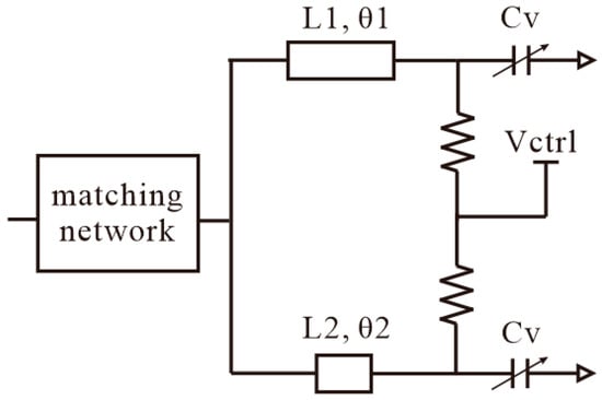
Figure 2.
Detailed configuration of tunable load termination.
The tuning mechanism of the parallel-LC topology can be summarized as follows: When the varactor capacitance is at its minimum, a series resonance occurs between L1, which is derived from the θ1 transmission line, and Cv. For intermediate capacitance values (Cmin < Cv < Cmax), the L1-Cv network becomes inductive, while the L2–Cv network becomes capacitive, creating a parallel resonance condition. When the capacitance reaches its maximum (Cv = Cmax), a series resonance forms between L2 and Cv.
Although the proposed approach achieves a wide phase-shifting range, it suffers from increased insertion loss and amplitude imbalance due to varactor loss, especially at low bias voltages where the varactor resistance is higher. To mitigate these effects, the matching network was carefully optimized to align the phase rotation axis with the center of the Smith chart, minimizing amplitude variation across the tuning range.
3.2. Phase Inverter
A parallel-strip phase inverter shown in Figure 3 is implemented using a signal-ground crossover structure to achieve a compact and bias-free phase inversion. The inverter exhibits an insertion loss of 4.9 dB at each port at 150 GHz, with amplitude variation kept below 0.3 dB across the 140~170 GHz band and a phase error of approximately 2.5° per 10 GHz. Compared with active phase-shifting approaches, the passive inverter offers inherently wide bandwidth and reduces DC power consumption by minimizing the number of required bias lines. Furthermore, unlike line-delay-based phase-shifting techniques, this design achieves lower amplitude variation and smaller footprint, as shorter transmission lines are sufficient to realize the desired phase shift. The phase difference is controlled by adjusting the dimensions of the ground slot, while gain balance is fine-tuned through the optimization of line width. This makes the proposed inverter well-suited for compact, low-power millimeter-wave and sub-terahertz front-end systems.
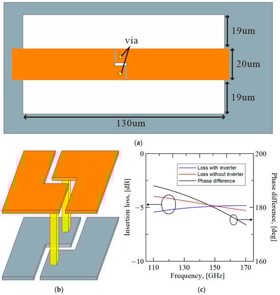
Figure 3.
Overall layout of parallel-strip phase inverter (a), detailed cross-over section (b), and EM-simulated S-parameter (c).
3.3. Amp Switch
A single-stage common-base amplifier topology is employed for the switch, enabling compact design and simple bias control. The switch achieves input matching better than −20 dB (S11) at 150 GHz and provides an on-off ratio exceeding 15 dB. In a standalone configuration, biasing is straightforward, while in phased-array implementations, the gate bias is applied globally, and the drain bias is controlled through a serial peripheral interface (SPI) to selectively switch devices on and off.
3.4. 90°. Coupler
A compact Lange coupler designed for D-band operation is implemented using a five-line coupled structure with multiple air-bridges to ensure equal potential across adjacent lines and maintain strong coupling. The coupler achieves a 90.1° phase difference between the through (S21) and coupled (S31) ports at 150 GHz, with a phase variation of 86°~92° across the entire D-band. Both S21 and S31 exhibit insertion losses of −4 ~ −4.2 dB with less than 0.2 dB amplitude imbalance over the band, while the return loss (S11) remains below −15 dB. The overall footprint of the coupler is 260 μm in length and 22.68 μm in width, making it highly suitable for integration in compact D-band front-end circuits.
4. Simulation Results of Full Circuit
The first phase-shifter architecture, which is shown in Figure 4, achieves a full 360° phase shift and operates over the 140–160 GHz frequency range. It exhibits an insertion loss of approximately −22 dB with a loss variation of 3.8 dB. The layout occupies 0.1 mm2, and only one bias line is required per channel, simplifying bias control. To achieve wideband operation, the inductance values were carefully tuned so that the phase-shifting range exceeds 360° at the center frequency, effectively minimizing amplitude mismatch caused by varactor capacitance variation.
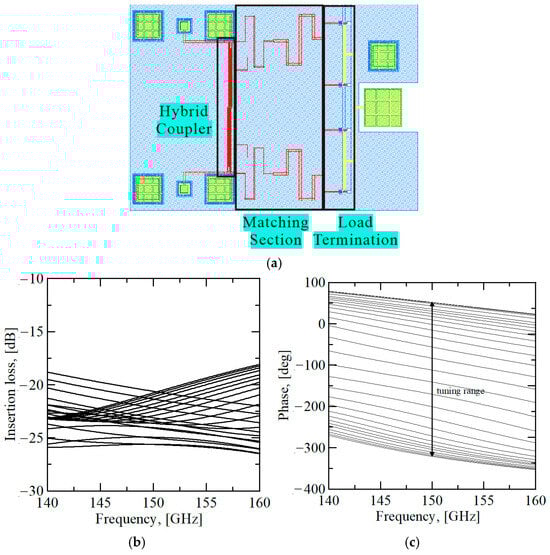
Figure 4.
Layout (a) and EM-simulated insertion loss (b) and phase (c) of 360° phase shifter design.
The second phase-shifter architecture, which is shown in Figure 5, provides a 180° phase shift and operates between 145 GHz and 153 GHz with an insertion loss of approximately −20 dB and a loss variation of 4.2 dB. However, if this design is interfaced with a differential port, such as a dipole transition, the two-way divider, combiner, and phase inverter can be eliminated, resulting in a gain improvement exceeding 5 dB. This optimization would enable performance comparable to prior works while maintaining a favorable loss profile, making this architecture highly advantageous for phased-array integration. The layout area is 0.3 mm2, and three bias lines are required per channel.
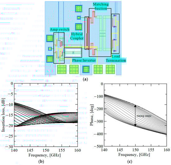
Figure 5.
Layout (a) and EM-simulated insertion loss (b) and phase (c) of 180° phase shifter design when differential port is connected.
5. Conclusions
This work presents two compact D-band reflection-type phase shifter (RTPS) architectures designed to achieve wideband and power-efficient phase control for phased-array applications. The first architecture demonstrates a full 360° phase-shifting range over 140–160 GHz using a parallel LC load termination and a single bias line, achieving minimized amplitude variation while maintaining a compact layout. The second design achieves a stable 180° phase shift with improved broadband characteristics and offers opportunities for gain enhancement and reduced loss when interfaced with differential ports. The proposed designs leverage passive components, such as a Lange coupler, reflective load, and passive phase inverter, to simplify biasing and minimize chip area and power consumption. According to the FoM comparison in Table 1, the proposed designs achieve the highest figure of merit among reported D-band CMOS implementations, confirming their superior efficiency and integration capability. These results demonstrate the effectiveness of the parallel LC load termination topology for realizing scalable and energy-efficient D-band beamforming systems.

Table 1.
Comparison of previously reported D-Band Reflection-Type Phase Shifters.
Author Contributions
Methodology, Y.K. and J.L.; Formal analysis, Y.K.; Data curation, Y.K.; Supervision, M.K. All authors have read and agreed to the published version of the manuscript.
Funding
This work was supported by the Institute of Information & Communications Technology Planning & Evaluation (IITP) grant funded by the Korea government (MSIT) (2021-0-00260, Research on LEO Inter-Satellite Links). The chip fabrication was supported by the IC Design Education Center (IDEC), Korea.
Data Availability Statement
Data are contained within the article.
Conflicts of Interest
The authors declare no conflict of interest.
References
- Kissinger, D. D-Band and Terahertz Frontends for 6G Wireless Communications in SiGe BiCMOS Technologies. In Proceedings of the 2022 IEEE MTT-S International Wireless Symposium (IWS), Harbin, China, 12–15 August 2022; pp. 1–3. [Google Scholar] [CrossRef]
- Maiwald, T.; Li, T.; Hotopan, G.-R.; Kolb, K.; Disch, K.; Potschka, J.; Haag, A.; Dietz, M.; Debaillie, B.; Zwick, T.; et al. A Review of Integrated Systems and Components for 6G Wireless Communication in the D-Band. Proc. IEEE 2023, 111, 220–256. [Google Scholar] [CrossRef]
- Kim, I.; Koo, H.; Kim, W.; Hong, S. A D-Band Differential Phase Shifter Based on a Transmission Delay Line with Variable Inductors and Capacitors. IEEE Microw. Wirel. Technol. Lett. 2025, 35, 59–62. [Google Scholar] [CrossRef]
- Muller, D.; Diebold, S.; Reiss, S.; Massler, H.; Tessmann, A.; Leuther, A.; Zwick, T.; Kallfass, I. D-Band digital phase shifters for phased-array applications. In Proceedings of the 2015 German Microwave Conference, Nuremberg, Germany, 16–18 March 2015; pp. 205–208. [Google Scholar] [CrossRef]
- Abbasi, M.; Lee, W. A Low-Loss Passive D-Band Phase Shifter for Calibration-Free, Precise Phase Control. IEEE J. Solid-State Circuits 2024, 59, 1371–1380. [Google Scholar] [CrossRef]
- Rio, D.D.; Gurutzeaga, I.; Berenguer, R.; Huhtinen, I.; Sevillano, J.F. A Compact and High-Linearity 140–160 GHz Active Phase Shifter in 55 nm BiCMOS. IEEE Microw. Wirel. Compon. Lett. 2021, 31, 157–160. [Google Scholar] [CrossRef]
- Testa, P.V.; Carta, C.; Ellinger, F. A 160–190-GHz Vector-Modulator Phase Shifter for Low-Power Applications. IEEE Microw. Wirel. Compon. Lett. 2020, 30, 86–89. [Google Scholar] [CrossRef]
- Sung, E.-T.; So, C.; Hong, S. A 60-GHz Variable-Gain Phase Shifter With Particular-Sized Digital-RF Cells. IEEE Trans. Microw. Theory Tech. 2022, 70, 1302–1313. [Google Scholar] [CrossRef]
- Chien, J.S.-C.; Buckwalter, J.F. A D-band, High Switching Speed, Differential Reflection-Type Phase Shifter in 250-nm InP HBT. In Proceedings of the 2022 17th European Microwave Integrated Circuits Conference (EuMIC), Milan, Italy, 26–27 September 2022; pp. 115–118. [Google Scholar] [CrossRef]
- Rao, S.G.; Cressler, J.D. A D-Band Reflective-Type Phase Shifter Using a SiGe PIN Diode Resonant Load. IEEE Microw. Wirel. Compon. Lett. 2022, 32, 1191–1194. [Google Scholar] [CrossRef]
- Yishay, R.B.; Elad, D. D-Band 360° Phase Shifter with Uniform Insertion Loss. In Proceedings of the 2018 IEEE/MTT-S International Microwave Symposium–IMS, Philadelphia, PA, USA, 10–15 June 2018; pp. 868–870. [Google Scholar] [CrossRef]
- Li, X.G.; Fu, H.P. A 100-GHz full 360° reflection-type phase shifter using a balanced phase inverter. Microw. Opt. Technol. Lett. 2020, 62, 1935–1939. [Google Scholar] [CrossRef]
- Kim, E.; Jeon, S. A D-Band Hybrid-Type CMOS Phase Shifter with Full 360° Phase Coverage. J. Electromagn. Eng. Sci. 2025, 25, 391–393. [Google Scholar] [CrossRef]


Disclaimer/Publisher’s Note: The statements, opinions and data contained in all publications are solely those of the individual author(s) and contributor(s) and not of MDPI and/or the editor(s). MDPI and/or the editor(s) disclaim responsibility for any injury to people or property resulting from any ideas, methods, instructions or products referred to in the content. |
© 2025 by the authors. Licensee MDPI, Basel, Switzerland. This article is an open access article distributed under the terms and conditions of the Creative Commons Attribution (CC BY) license (https://creativecommons.org/licenses/by/4.0/).