Abstract
The most common method used to pick up biomedical signals is through metallic electrodes coupled to the input of high-gain, low-noise amplifiers. Unfortunately, electrodes, amongst other effects, introduce an undesired contact resistance and a contact potential. The contact potential needs to be rejected since it would otherwise cause the saturation of the input stage of the amplifiers, and this is almost always obtained by inserting a simple RC high-pass filter in the input signal path. The contact resistance needs to be estimated to ensure that it does not impair correct measurements. Methods exist for estimating the contact resistance by dynamically modifying the input network configuration, but because of the presence of the input RC filter, long transients are induced any time a switch occurs between different input configurations, so that the measurement time may become unacceptably long. In this paper, we propose a new topology for a DC removal network at the input of the differential signal amplifier that results in an AC filter whose time constant can be continuously changed by means of a control voltage. As such, we can speed up the recovery from transients by setting very short time constants (during the input resistance estimation process) while maintaining the ability to obtain very low cut-in frequencies by setting a much larger time constant during actual measurements. A prototype of the system was built and tested in order to demonstrate the advantage of the approach we propose in terms of reduced measurement time.
1. Introduction
Biological acquisition systems are commonly designed with a low-noise voltage amplifier (LNA) as a front-end [1]; recent research shows, for example, low-power and low-noise configurations [2,3] and differential and high-CMRR circuits for EEG acquisition [4,5]. These amplifiers are almost always differential and with a band that extends from DC, as reported in [6,7]; even when the electrode is of the capacitive type, the amplifier is designed as a directly coupled one [8].
The electrical behavior of the contact between the patient and the amplifier is complex [9,10]; it is often nonlinear and, even when linear models are used, frequency-dependent. However, with the exception of capacitive electrodes, two elements are always present: a series resistance and a series DC potential, called the half-cell potential. The series resistance is detrimental to the quality of the measured signal [11,12,13], both because of the added noise and the attenuation that results when considering the input resistance of the amplifier; it is paramount to monitor its value when performing measurements. The half-cell potential is often much bigger than the signals of interest. As the amplifier designs usually present a high gain, they may saturate if the input signal is not properly conditioned.
As a consequence, removing the DC component of the input signal is a necessary stage when low-voltage signals are acquired. Especially in the case of neurophysiological monitoring, adhesive or needle electrodes are connected to the subject being monitored [14,15,16]; the half cell potential of the two electrodes between which the measurement is carried out are never exactly the same, causing an inherent differential voltage in the contact circuit. This results in a DC offset in the input signal that has to be removed [17,18].
A common solution is to use a high-pass (HP) RC (resistance-capacitor) filter. The corner frequency of the high-pass filter must be quite low, in the order of tenths of Hertz, to account for the band of several physiological signals. This results in very slow settling times (in the order of tens of seconds) for the whole system. In other words, the low corner frequency allows a constant response in the band of interest, but increases the time response when the input voltage is affected by a steep change due to the large RC value.
A long settling time is not only a problem when connecting and disconnecting the system to the subject: changing the input configuration with the subject connected to the amplifier also causes transients. In addition to the filtering and amplifier stages, monitoring systems are usually fitted with the circuitry necessary to measure contact impedance; a too high contact impedance is a sign of a poor or deteriorating contact and can strongly affect the quality of the measurement. Generally, the impedance assessment circuit consists of a generator that injects a current into the patient [19,20,21], usually by means of a square or sinusoidal signal. This methodology also implies stopping and resuming the acquisition process for a period of time. In [22,23], a novel passive method is presented, consisting of analyzing the voltage variation when parallel loads are connected to the input of the system, thus preventing the injection of current.
The approach in [22] consists of continuously monitoring the biopotential source. When an impedance measurement is needed, several electronic switches are acted upon so that several known resistors are connected in parallel to the input signal path. If the sources are ideal (zero connection impedance), no voltage change would be expected; conversely, the presence of a contact impedance will degrade the input signal [20]. Assessing the contact impedance is, however, not trivial as the source signal is essentially unpredictable. In most cases, the exact value of the impedance is not needed: assessing whether it is low enough to guarantee a correct measurement is sufficient in many cases. Literature and current clinical practice set an approximate value of 5 KΩ as the limit for most common monitoring techniques such as EEG or evoked potentials [24,25,26]. Several statistical characteristics and estimation methods have been used to predict the impedance value from the registered signal [19]. In [22], observing and computing the changes in the input signal during the impedance measurement cycle enabled us to detect if the impedance was within an acceptable range.
The main problem with the procedure of connection and disconnection of the additional loads is that it causes changes in the DC values of the equivalent input sources, thus triggering long transients that need to be extinguished before actual measurements can be obtained. Therefore, the lower the cut-in frequency, the longer the time needed to complete the measurements required for the characterization of the contact impedance.
Ideally, we would like to be able to speed up the transients during the changes in the input circuit configuration and return to the low cut-in frequency configuration as soon as the transients are extinguished. Of course, such an approach would be effective only if we are able to avoid the introduction of further transients when switching back from a higher cut-in frequency (resulting in faster transients) to a lower cut-in frequency (required for extending the measurements in the low frequency range).
In [27], a new method is proposed to address a similar issue that consists of the integration of an active loopback to compensate for the DC offset of the signal. This is obtained due to a current generator that charges and discharges a capacitor in series with the input of the amplifier. This capacitor acts as a floating voltage source that cancels the variation in the DC voltage at the input much faster than a common RC filter. An intrinsic nonlinearity is exploited in order to obtain fast transients upon large and abrupt changes in the input while retaining a very low cut-in frequency when such transients are extinguished. However, in [27], there is no direct control on the input filter cut-in frequency, as would be desirable for our application.
The aim of this study is to extend and adapt the method presented in [27] to the case of a differential amplifier for bio-potential measurements by introducing the ability to employ a control voltage for setting the cut-in frequency. This approach, as will be shown in the experimental section, allowed us to dramatically reduce the time required to perform impedance measurements with the method outlined in [22]. This time reduction is significant, since it allows us to effectively address and solve the most important drawback of the approach in [22].
2. Proposed Approach
In this section, we describe how we propose to solve the problem of having an AC-coupled amplifier that can be smoothly switched from a configuration where it has a very low cut-in frequency (and therefore very long time constant that generates slow transients) to one where the cut-in frequency is higher but with faster transients. Firstly, we summarize the case for a single-ended amplifier based on the active filter presented in [27] and adding the proper circuitry to allow the active filter to be controllable with an external voltage; finally, we extend the principle to a fully differential amplifier topology.
2.1. Single-Ended Amplifier
As outlined in the Introduction, the main problem with performing the estimation of the contact impedance using a purely passive approach is that it requires repeated measurements while changing the input circuit configuration by means of switches. Any time a switch is moved to short the input or connect and disconnect resistances in the signal path, long transients are induced because of the very low input cut-in frequency of the system. This translates into quite long measurement times that might not be acceptable in a number of situations.
While a low cut-in frequency is required in order to not lose information during actual measurements on the patient, higher cut-in frequencies could be tolerated during the contact impedance estimation process.
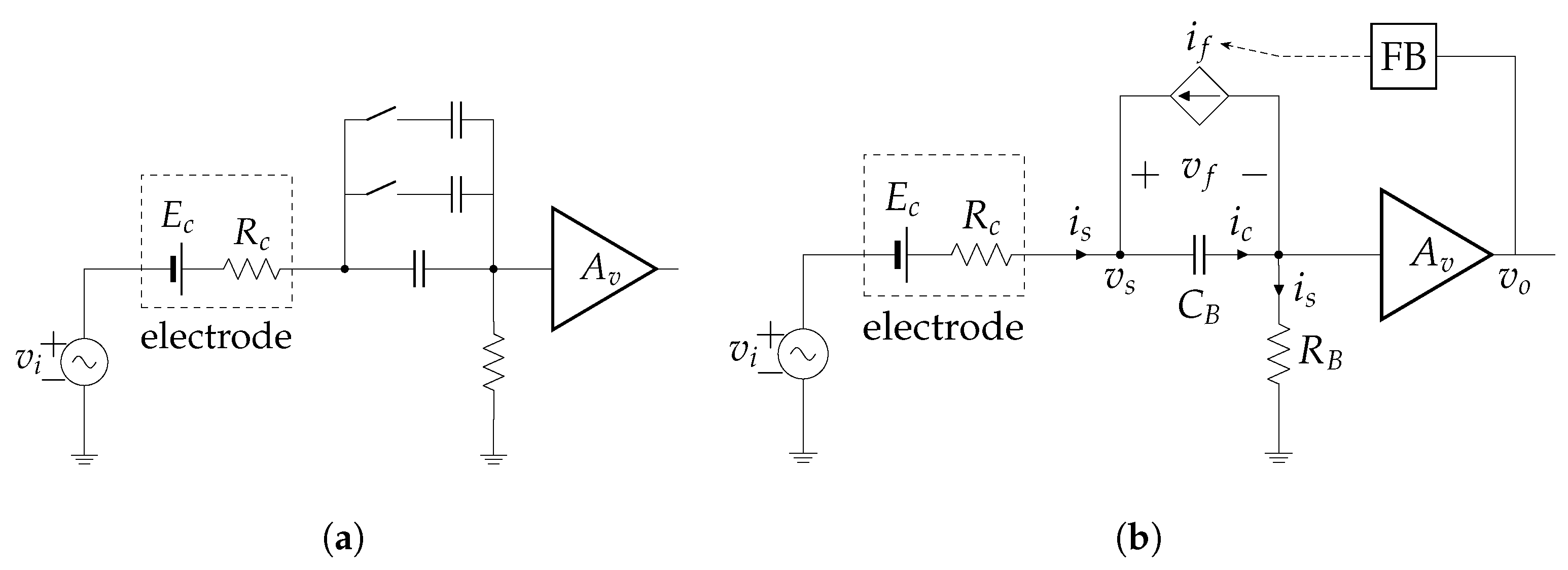
A simple method to obtain an AC-coupled amplifier with an adjustable cut-in frequency would be to resort to a number of electronic-controlled switches to change the blocking capacitor in the input path, as shown in the simplified diagram in Figure 1a. With a larger capacitance (switches closed), we obtain a lower cut-in frequency; by disconnecting some of the capacitors, we increase the cut-in frequency. During transients, we may open all or some of the switches to obtain a high cut-in frequency, thus speeding up the transients, and when the transients are extinguished, we can close all switches to obtain the largest equivalent capacitance and, hence, the lowest cut-in frequency.

Figure 1.
Simple (a) and proposed (b) amplifier topology for obtaining a variable bandwidth. The current generator is controlled by the output voltage if = Gmvo, where Gm is the transconductance gain.
The obvious problem with this approach is that the capacitors connected to open switches would be charged to voltage levels that are, in general, different from those of the capacitors still connected in the circuit. Therefore, when the previously disconnected capacitors are switched back in, to obtain the lowest cut-in frequency, an almost instantaneous charge redistribution occurs. This results in a voltage step whose amplitude depends on the previous history and that, in turn, results in a transient that will evolve with the time constant corresponding to the lowest cut-in frequency, thus making the approach just described completely useless.
If we want to effectively reduce the set-up time, a system must be devised for switching from a high cut-in frequency to a low cut-in frequency, minimizing the transient time. The approach we developed to address this issue relies on the design of an auxiliary system that acts upon the main circuit in so that the lower cut-in frequency can be continuously adjusted by a voltage signal, thus allowing for gradual transitions from one configuration to another. Moreover, when the steady state is reached with the lowest cut-in frequency, the auxiliary system is essentially deactivated and does not contribute in any way to the actual measurements on the patient.
It is interesting to reflect on the fact that the presence of a capacitor in series with the signal path in a voltage amplifier merely blocks the DC component across the source. We can look at the transients as the time required for the capacitor to change to a DC voltage that subtracts from the input DC component so that the high gain stages of the amplifier do not saturate. From this view, in order to reduce the transient time, we need to find a method to speed up the charging of the input capacitor at the correct value without interfering, if at all possible, in the overall response of the system during actual measurements. This approach was followed in [27] in the case of a single-ended amplifier for low-frequency noise measurements in a situation in which the maximum peak-to-peak voltage of the input signal was not expected to exceed a few tens of microvolts, and the availability of a control voltage for directly controlling the cut-in frequency was not necessary.
In this paper, we exploit the basic concept developed in [27] and show how we can obtain a voltage-controlled cut-in frequency and how this can be extended to the case of a differential amplifier with adjustable bandwidth. In order to simplify the discussion, let us start with the case of a single-ended amplifier, as in the schematic diagram in Figure 1b. We essentially add an auxiliary system to what would otherwise be a conventional AC-coupled amplifier. Such an auxiliary system reduces to the feedback block (FB) controlling the value of the current charging the capacitor . The entire auxiliary system can be regarded as a voltage controlled floating current source and can be easily implemented using integrated photovoltaic couplers, as in [27].
A key observation is that, if the FB sets the current to a constant 0, the auxiliary circuit would have no effect on the circuit response, and we might as well remove the auxiliary system from the amplifier. In general, however, the FB operates according to the following equation:
Since we are interested in the behavior of the system at low frequencies, we can assume the gain of the amplifier is constant (i.e., independent of the frequency). Moreover, assuming, as is often the case, , we can easily obtain the overall response of the system in the Laplace domain as follows (we use capital letters for quantities in the Laplace domain):
The result in Equation (4) shows that that we obtain a high pass response with a cut-in frequency given by:
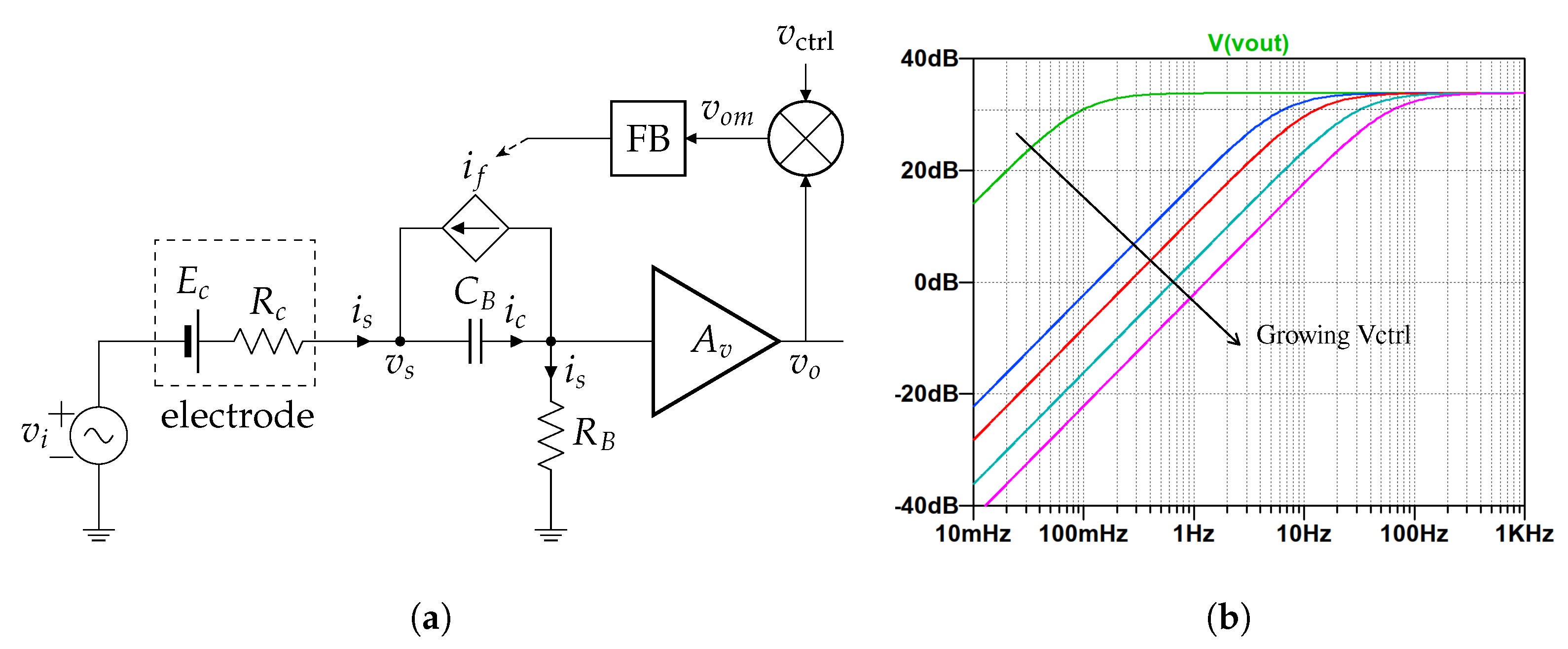
As we anticipated, if , the cut-in frequency corresponds to the one set by the passive AC filter - in the input path. Moreover, from Equation (5), it is apparent that we can change the value of the cut-in frequency by changing the gain . Since we want to be able to control the value of the cut-in frequency by means of a control voltage, we modified the approach followed in [27] by adding an analog multiplier in the path from the output of the amplifier to the input of the FB block, as shown in Figure 2a. Assuming a constant control voltage , we have:
where is the multiplier scaling factor. Now has the same form as in Equation (4), except that we have, for and :
from which it is clear that we can change the cut-in frequency by adjusting the control voltage . Note that whatever value of is set with the circuit discussed so far, in the pass-band (i.e., for ), the input impedance of the amplifier remains unchanged and equal to . As an example of the results that could be obtained in term of frequency response, Figure 2b shows the result of SPICE simulations performed with typical values of the circuit parameters that can be experienced when implementing the FB, as in [27].
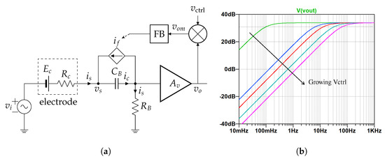
Figure 2.
Controlling the feedback loop (with a variable-gain amplifier or a multiplier) enables an external controlling voltage: (a) the basic circuit; (b) the results of the LT-SPICE simulation with Gm = 80 μΩ−1, kv = 1 V−1, Av = 50 V/V, CB = 10 μF, RB = 160 kΩ, Ec = 0 V, Rc = 5 kΩ, over several values of the controlling voltage.
2.2. Extension to a Differential Amplifier
Extending the approach we discussed above to the case of a differential amplifier requires some caution. In a single-ended amplifier, the error signal at the input of the FB is proportional to the output voltage, which is directly proportional, as in Equation (2), to the difference between the input signal and the voltage across the coupling capacitor . In a differential configuration, we have two blocking capacitors, and , as in Figure 3. If we indicate with and the input voltages and with and the voltages at which and are charged, respectively, we have:
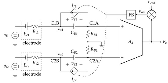
Figure 3.
Simplified schematic diagram of the differential case.
We must therefore devise a strategy in order to use the output voltage for inducing a change in the voltages and across the blocking capacitors. The decision taken in this study was to induce equal and opposite changes in the voltages and , i.e., to ensure that it is at all times.
With this choice, the FB block only acts on the dynamics of the differential signal: if a step occurs at the inputs, resulting in a step in the common mode voltage together with a step in the differential voltage , the FB will only react to the change in , with the dynamics of evolving as if the FB was not present.
To be more precise, if a pure common mode step is presented at the input, this will not be sensed by the FB, since the instantaneous voltages at the inverting and noninverting inputs of the instrumentation amplifier would be ideally the same during the transient. In this case, and in the absence of any other signal following the common mode input step, the inputs of the instrumentation amplifier evolve toward zero with a time constant , regardless of the setting of the FB.
Up to this point, we assumed ideal behavior for the instrumentation amplifier and, in particular, we assumed no offset to be present. The presence of the offset, however, needs to be carefully discussed in view of how we plan to employ the FB.
If both the input offset voltage and the input offset current are null (i.e., if the bias currents are the same on each input), the steady state corresponding to a constant common mode voltage at the inputs of the system is . The input bias currents of the instrumentation amplifier flows through the resistances and and produces a purely common mode voltage at the inputs (resulting in ). In this situation, switching on and off the FB produces no transient on the system.
However, if an offset is present, when the FB loop is active, it tends to compensate for such an offset by forcing opposite currents at steady state in order to produce a differential input, compensating the intrinsic offset of the instrumentation amplifier. In this situation, when we switch off the FB, we necessarily introduce a transient, which, since the FB is disconnected, evolves with the smallest time constant of the circuit. The amplitude of the transient and the time required for its effect to become negligible depend on the magnitude of the offset. This effect is likely to be small in most situations. However, in order to ensure that it is negligible and that we take full advantage of the proposed approach, we need to guarantee that we can act on the system in order to compensate for the offset of the instrumentation amplifier. Adding a circuit for offset compensation and making it automatic so that the final user need not worry about it would be quite simple. As we show in the next section, in order to minimize the complexity of the prototype, we opted for a manual compensation approach. However, the compensation setting does not depend on the source impedance, which means that it needs to be performed only once and checked from time to time.
3. Results
To showcase the new amplifier design, we built a fully functional prototype. We then applied it to replace the front-end amplifier of the system in [22], tackling the problem of the passive measurement of contact resistances. In this section, we first introduce the details of the implementation, providing a complete prototype schema. Then, we show that the new circuit topology can markedly reduce the time needed to perform contact resistance estimation.
3.1. Prototype
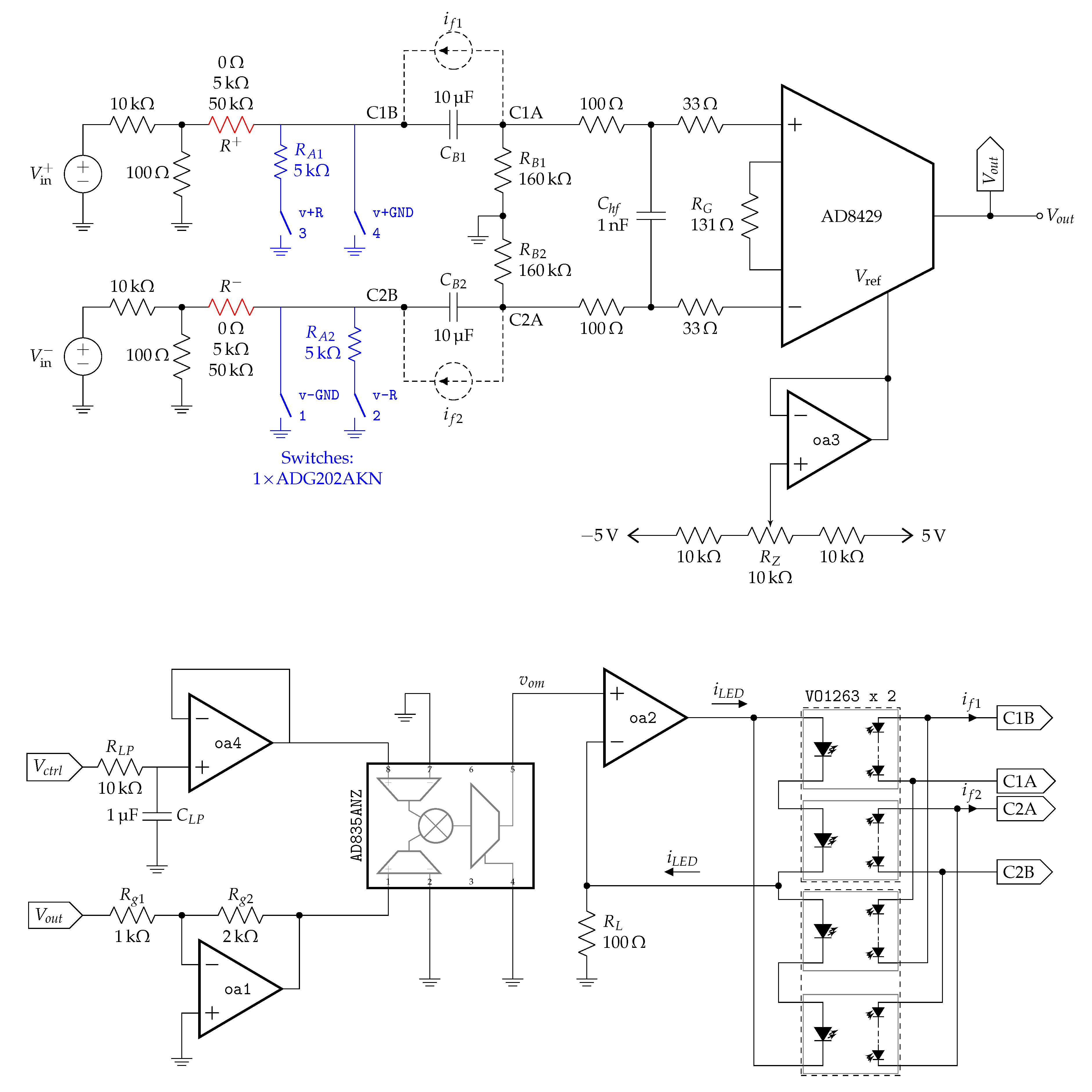
A prototype was built and tested to demonstrate the effectiveness of the proposed approach. A low-noise AD8429 amplifier was chosen for the differential measurement, and configured for a gain of 50 V/V, similar to the system in [22].
The main difference with respect to [22] is the presence of the two floating current sources and across the capacitors and in the top portion in Figure 4, which represent the action of the FB whose detailed implementation is reported in the bottom portion of the figure.
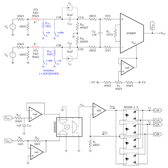
Figure 4.
Full circuit used in the tests. The components without labels were added following the suggestions of the respective data sheets, so they are not substantial for the discussion of the behavior. The upper circuit is the main amplifier with the switches used to check the contact impedance, simulated by the and resistors (together with the equivalent output resistance of the divisor used to reduce the input voltage range). The lower circuit is the FB, consisting of a multiplier, , and current injection stage. All the components were supplied with a symmetric V source.
Switches from 1 to 4 were used to change the configuration of the input section of the system. Following [22], these were operated to perform a series of measurements from which the contact resistances were estimated. As noted above, the task of the FB is to speed up the recovery of the system from the transients induced by repeated changes in the configuration of the switches.
The operation of the differential amplifier in the absence of the floating current sources is discussed in [22]. A circuit was built around the operational amplifier OA3 to enable the fine adjustment of the offset of the system (when the FB was inactive), avoiding transients when the FB was deactivated following a change in the switch configuration.
The implementation of the FB was based on two integrated dual photo-voltaic MOSFET drivers (VO1263). Each VO1263 essentially contains two miniaturized solar cells, each with its own light emitter source in the form of an integrated LED. As discussed in [27], a single VO1263 can be used to obtain a current-controlled floating current source capable of delivering positive and negative currents in the order of a few microamperes with a voltage compliance in excess of 10 V. In our prototype, two VO1263 were combined to form a dual floating current source, with nominally opposite currents, controlled by the current at the output of OA2 in Figure 4.
The transfer coefficient from the driving current toward the output current is typically in the order of 2 × 10⁻³ A/A for driving currents above a few tens of microamperes, as illustrated in Figure 5. This plot also shows that the behavior is not linear for low output currents. This is not a limitation in our case since the FB is used merely to speed up the transients after the switch configuration changes.
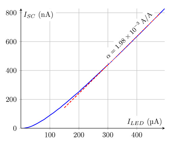
Figure 5.
Input-output characterization of the optocoupler. is the input current and is the short-circuit output current.
In ideal conditions, toward the end of the transients, we should be approaching and . The decrease in the slope of the input-output curve in Figure 5 for low currents means that the effectiveness of the feedback decreases as well. Consequently, we obtain a disengaging effect of the FB close to the steady state, which helps to smooth the the transition from active to inactive FB at the end of the transients.
The voltage multiplier AD835 was used to change the feedback gain from the voltage toward the currents and , by means of the voltage . If we neglect, for the moment, the effect of the low pass filter -, the voltage at the output of the multiplier is:
with −1 in the case of the AD835.
The voltage at the output of the multiplier drives a voltage-to-current converter implemented with the operational amplifier OA2, so that the current through the LEDs inside the VO1263 devices is:
Note that when , the two upper LEDs in Figure 4 are “on” and the two bottom LEDs are “off”; when , the two upper LEDs are “off” and the two bottom LEDs are “on”.
Finally, including the transfer coefficient , the gains and from the output voltage to the currents and are:
with the values of the parameters in Figure 4. When is at the maximum value of 1 V, the gains amount to:
Extending the results in Equation (7) to the case of the differential configuration, when the FB is active with , we obtain a low-pass limit that is 160 times larger than the low-frequency corner corresponding to the time constant , i.e., about 16 instead of 100 . When is 0, the FB is inactive and the low-frequency corner is set by and , which is 100 .
Finally, a low-pass filter -, with a time constant of 10 , was added to the control signal in the input of the multiplier control voltage and used to smooth the gain change in the feedback loop.
The remaining differences in the full circuit in Figure 4 with respect to that in Figure 3 were implementation details, applied following the recommendations in the component’s data sheets.
A separate microcontroller board provided the output in a 0–1 range and was also used to control the switches when performing the source resistance assessment.
3.2. Measurements on the Prototype
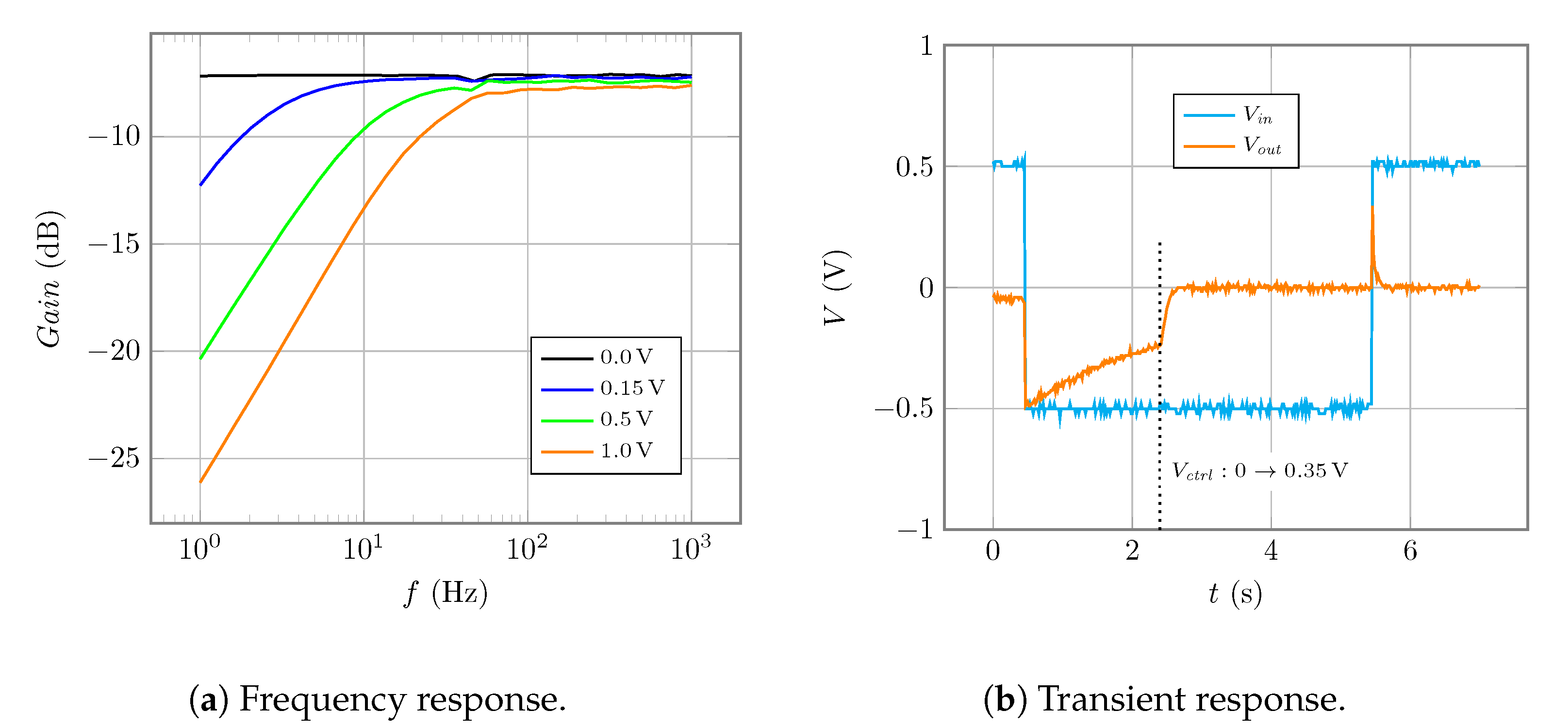
Although the system is, strictly, nonlinear for small values of feedback loop signal (due to the aforementioned nonlinearity in the coupling devices, which makes the loop inactive for very small signals), we tested the frequency response with relatively large signals, keeping the output voltage as high as possible, around 2 peak-to-peak. The result (measured in the range 1 –1000 ) is provided in Figure 6a; the behavior is basically the same as that shown in Figure 2b.
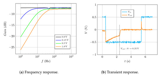
Figure 6.
(a) The measured frequency response (please see the main text) for different values of vctrl; (b) transient response when vctrl is changed abruptly from 0 to 0.35 V at t = 2.5 s.
In the time domain, the behavior of the amplifier was checked by applying a pure differential square voltage to the amplifier input (cyan line in Figure 6b) with the feedback loop disabled (); at a certain point in time, is abruptly raised to a value of V (not shown in the diagram; the switching instant is marked with a dotted vertical line).
The exponential transient of the output (orange line) before the change shows the natural hard response of the circuit, with a time constant in the order of ten seconds. As soon as the feedback loop is enabled, the system smoothly switches to a much faster response, as can be easily deduced from the shape of the following transient. In conclusion, we can speed up the circuit when we expect large transients due to the switching of the input configuration during the resistance measurement phase, and switch back to the normal behavior for the measurement phase.
3.3. Application to Resistance Estimation
Similar to the procedure in [22], the parallel connection circuit is managed with a digitally-controlled switch and a microcontroller that activates and deactivates the corresponding connections within the four configurations necessary to complete the impedance measurement. To summarize the procedure, the RMS of the signal is first estimated over a selectable period , and then measured again over the same for each switch configuration reported in Figure 7b. From this information, we can calculate the approximate values or the contact resistance. The mathematical details can be found in [22].
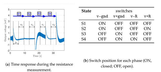
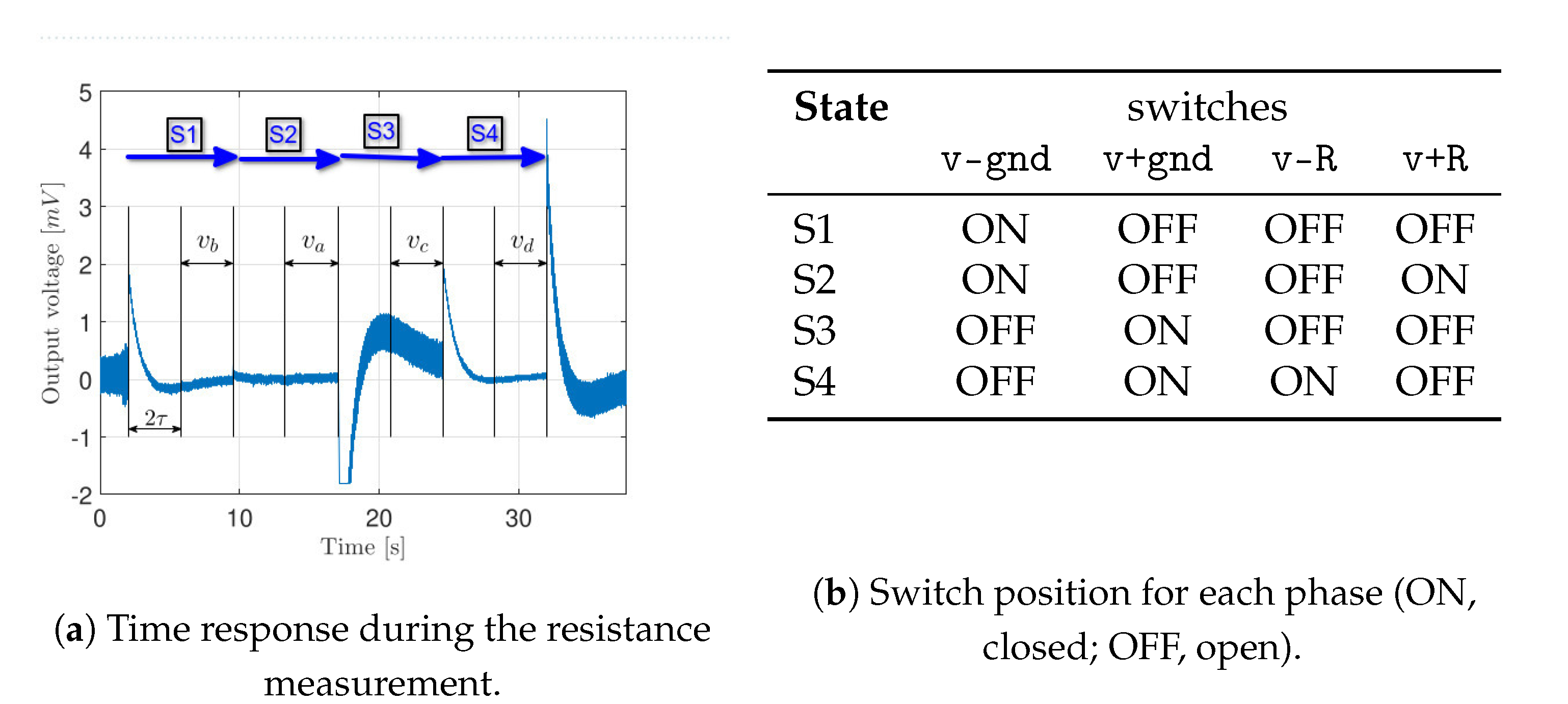
Figure 7.
Example of the output of the amplifier during the resistance measurement in the system described in [22]. S1 to S4 are the four configurations of the input switches for each stage; normal operation is with all switches off. The table in (b) specifies the switch position for each stage.
In the original system, the switching phase lasted at least 30 due to the time needed to wait for the end of the transient. One example sequence of measurement, for the four different switch configurations, is shown in Figure 7a.
Since this kind of system is intended for input voltages in the range of microvolts or millivolts, the waveform generator that emulated the input signal in our tests was followed by a resistor attenuator. The differential signal was obtained by a linear circuit with adders and a difference amplifier circuit (not shown) so that we generated two signals with known common and differential mode components. The differential input signal used as a test signal was a sinusoidal waveform with a frequency of Hz and an amplitude around mV peak-to-peak. The common mode was a similar sinusoidal signal, at the same frequency, with a 20 mV amplitude as well.
During the switching phases, the signal was set high, and then re-set to zero after the output amplitude and RMS were measured.
To test the system, we set and to known values: in this case 100 , 5 KΩ, and 50 KΩ, which correspond to a good, middling, and poor contact, respectively. The resistance values obtained with the procedure outlined above were then compared with the known value of contact resistance.
Figure 8 contains the output voltage ( in Figure 4) of one of the impedance measurements corresponding to the impedance values and . The transients are much more subdued than those in [22], and the measurement can be carried out in a shorter time.
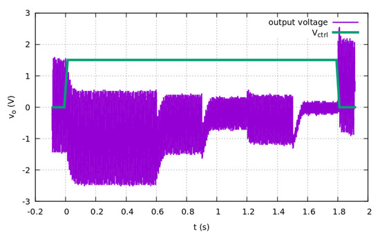
Figure 8.
Example of the output voltage from the prototype for KΩ and KΩ, switching every 400 . The base signal is a 100 sinusoidal one; it is evident that the transients are fast when the control voltage is high.
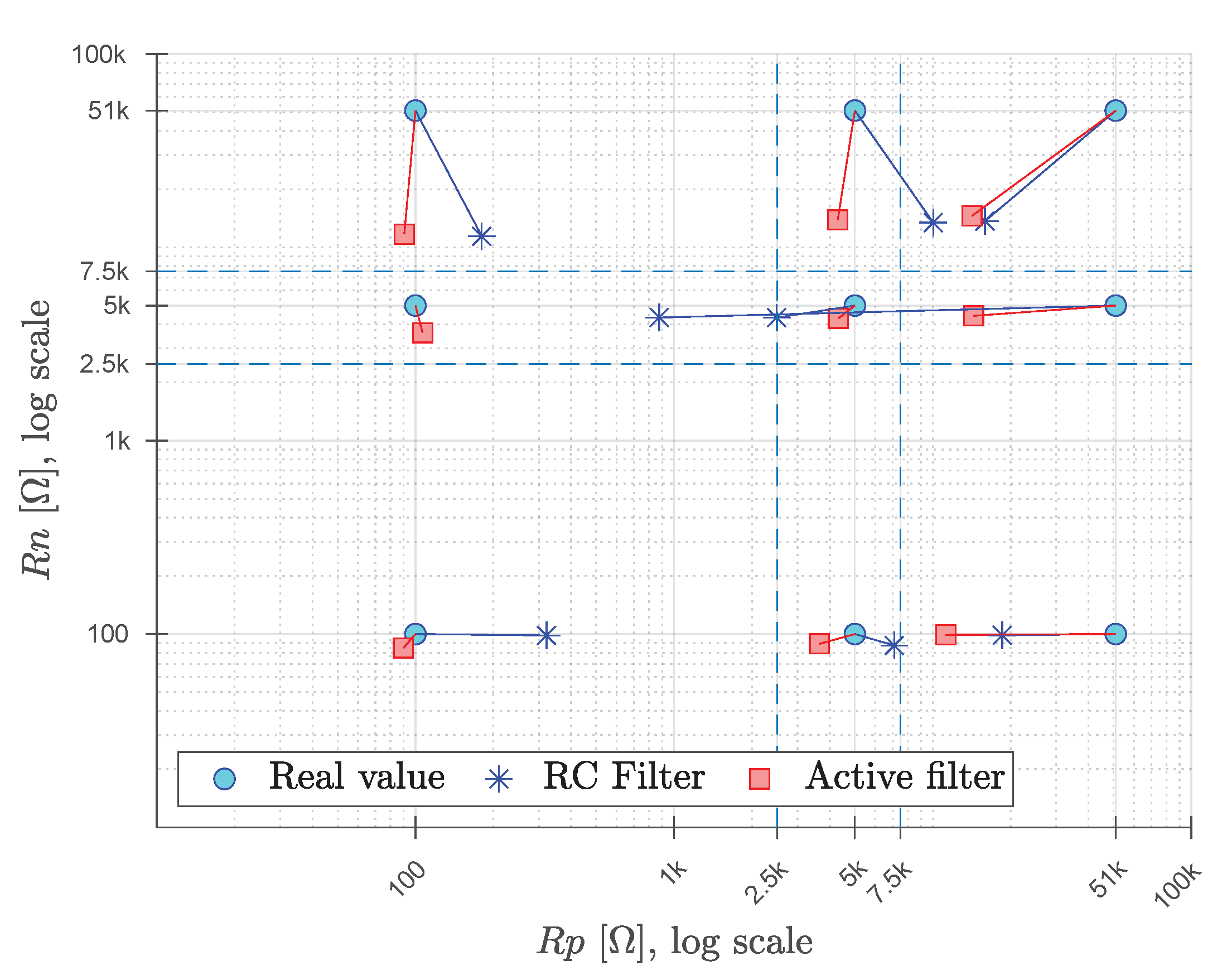
Finally, Figure 9 shows the result of the passive resistance measurement performed across all possible combinations of the three chosen values of contact resistance, comparing the results obtained with the approach in [22] (RC filter) with the methodology proposed in this paper (active filter) considering the enhanced, shorter measurement time. The active filter enables a better global resistance assessment and avoids false positives (detecting poor contact resistance as good or middling) which is the main objective of the system.
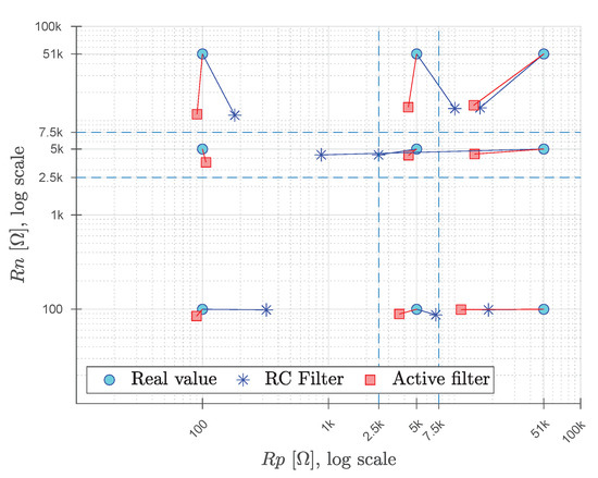
Figure 9.
Resistance assessment result, with a switching period of 1 . The cyan dots are the real values of the contact resistance, the red squares are those estimated using the active filter, and the blue stars are the values estimated with the RC filter.
4. Discussion
As previously stated, one of the main drawbacks of the original impedance measurement methodology proposed in [22] is the time needed for the completion of the contact resistance estimation process, due principally to the transient responses triggered by the steep changes in the input voltage. In the case of the original RC filter circuit, and considering a balance between accuracy and latency, a safety period proportional to the time constant of the high pass filter is required before starting the RMS calculation (chosen as representative statistical measurement) in order to avoid the transient effect. A typical measurement with that system is shown in Figure 7a; the time spent performing the contact resistance measurement is in the order of a minute (around 30 in the case of the measurement shown).
The time constant with the active filter is much shorter, which means that the safety period can also be shortened in the same order of magnitude. The new system settles much faster than the older system, as can be seen by comparing Figure 7a and Figure 8.
The results of the resistance detection, as shown in Figure 9, are slightly worse in absolute value than those obtained in [22]. However, the time spent in the resistance measurement is at least one order of magnitude less than that needed without the active filter topology. In the end, the only relevant information for the monitoring devices is if the contact is good enough. In Figure 9, note that no contact resistance configuration lying outside the quadrant where both contact resistances are low (the lower left one) is mis-detected as good. The absence of such a case shows that there are no false positives in the detection, which confirms the suitability of the approach.
In addition to the application shown here, a similar topology can be applied to all the cases where a differential amplifier needs to be designed with a high-pass filter with very low cut-in frequency, while a fast settling time is advantageous during the phases of connection and re-connection of the system to the signal sources.
5. Conclusions
In this paper, a new topology was proposed to design AC-coupled differential amplifiers with a cut-in frequency that can be continuously changed through a control voltage. This feature allows us to speed up the recovery from transients by setting very short time constants (when large transients occur at the input) while maintaining the ability, by setting a much larger time constant during actual measurements, to obtain a flat response down to very low frequencies. A prototype of an amplifier employing the proposed topology was built, tested, and used to speed up a recently proposed measurement procedure to determine the contact resistance due to electrodes in bio-signal measurement experiments. This procedure, based on measurements performed after provoking controlled changes in the input network configuration, while effective, was limited by the presence of long transients after each change occurs. With the prototype we built, comprising an adjustable AC input filter with a time constant ranging from 8 ms up to s, it was possible to reduce the overall measurement time for the determination of the parasitic resistances from about 30 s to about 5 s. The new circuit shows no degradation in sensitivity and in the lowest frequency that can be explored during signal acquisition.
Author Contributions
Conceptualization, R.G., C.C. and G.S.; methodology, E.A.R., C.R.-M.G.; software, E.A.R., C.R.-M.G. and R.G.; validation, R.G. and E.A.R.; formal analysis, C.C. and G.S.; investigation, E.A.R., G.S., C.C., C.R.-M.G. and R.G.; resources, C.R.-M.G.; writing—original draft preparation, E.A.R., C.C., G.S. and R.G.; writing—review and editing, G.S., C.C., C.R.-M.G. and R.G.; visualization, R.G.; project administration, C.R.-M.G. All authors have read and agreed to the published version of the manuscript.
Funding
This research received no external funding.
Data Availability Statement
Measurement and simulation data are fully available upon request.
Acknowledgments
The authors would like to acknowledge the support from the technical personnel at the Universidad Pontificia Comillas laboratories, namely José María Bautista and Antonio Martínez. They would like to acknowledge the collaboration with Analog Devices, for providing a ADALM-2000 system that was partially used for the building of the prototype. Finally, they would like to thank Christopher Michael Turner for the English language help and review.
Conflicts of Interest
The authors declare no conflict of interest.
Abbreviations
The following abbreviations are used in this manuscript:
| LNA | Low-noise amplifier |
| RMS | Root mean square |
| HP, HPF | High pass (filter) |
| RC filter | Resistance-capacitor filter |
| FB | Feedback block |
| DC | Direct current (used for continuous signals) |
| AC | Alternating current (used for variable signals) |
References
- Webster, J.G. Medical Instrumentation Application and Design, 4th ed.; Wiley: Hoboken, NJ, USA, 2009. [Google Scholar]
- Simmich, S.; Bahr, A.; Rieger, R. Noise Efficient Integrated Amplifier Designs for Biomedical Applications. Electronics 2021, 10, 1522. [Google Scholar] [CrossRef]
- Kim, J.; Ko, H. A Dynamic Instrumentation Amplifier for Low-Power and Low-Noise Biopotential Acquisition. Sensors 2016, 16, 354. [Google Scholar] [CrossRef] [Green Version]
- Chebli, R.; Ali, M.; Sawan, M. High-CMRR Low-Noise Fully Integrated Front-End for EEG Acquisition Systems. Electronics 2019, 8, 1157. [Google Scholar] [CrossRef] [Green Version]
- Ruiz-Amaya, J.; Rodriguez-Perez, A.; Delgado-Restituto, M. A Low Noise Amplifier for Neural Spike Recording Interfaces. Sensors 2015, 15, 25313–25335. [Google Scholar] [CrossRef] [PubMed] [Green Version]
- Bansal, M.; Srivastava, G. Design and Implementation of LNA for Biomedical Applications. In Intelligent Computing, Information and Control Systems; Pandian, A.P., Ntalianis, K., Palanisamy, R., Eds.; Springer International Publishing: Cham, Switzerland, 2020; pp. 154–167. [Google Scholar]
- Ruiz-Amaya, J.; Rodríguez-Pérez, A.; Delgado-Restituto, M. A review of low-noise amplifiers for neural applications. In Proceedings of the 2010 2nd Circuits and Systems for Medical and Environmental Applications Workshop (CASME), Merida, Mexico, 13–15 December 2010; pp. 1–4. [Google Scholar] [CrossRef] [Green Version]
- Portelli, A.J.; Nasuto, S.J. Design and Development of Non-Contact Bio-Potential Electrodes for Pervasive Health Monitoring Applications. Biosensors 2017, 7, 2. [Google Scholar] [CrossRef] [PubMed] [Green Version]
- Alimisis, V.; Dimas, C.; Pappas, G.; Sotiriadis, P.P. Analog Realization of Fractional-Order Skin-Electrode Model for Tetrapolar Bio-Impedance Measurements. Technologies 2020, 8, 61. [Google Scholar] [CrossRef]
- Chi, Y.M.; Jung, T.p.; Cauwenberghs, G. Dry-Contact and Noncontact Biopotential Electrodes. IEEE Rev. Biomed. Eng. 2010, 3, 106–119. [Google Scholar] [CrossRef] [PubMed] [Green Version]
- Kappenman, E.S.; Luck, S.J. The effects of electrode impedance on data quality and statistical significance in ERP recordings. Psychophysiology 2010, 47, 888–904. [Google Scholar] [CrossRef] [PubMed] [Green Version]
- Buxi, D.; Kim, S.; Van Helleputte, N.; Altini, M.; Wijsman, J.; Yazicioglu, R.F.; Penders, J.; Van Hoof, C. Correlation between electrode-tissue impedance and motion artifact in biopotential recordings. IEEE Sens. J. 2012, 12, 3373–3383. [Google Scholar] [CrossRef]
- Taji, B.; Shirmohammadi, S.; Groza, V.; Batkin, I. Impact of skin-electrode interface on electrocardiogram measurements using conductive textile electrodes. IEEE Trans. Instrum. Meas. 2014, 63, 1412–1422. [Google Scholar] [CrossRef]
- Musteata, M.; Borcea, D.G.; Ștefănescu, R.; Solcan, G.; Lăcătuș, R. Influence of Stainless Needle Electrodes and Silver Disk Electrodes over the Interhemispheric Cerebral Coherence Value in Vigil Dogs. Sensors 2018, 18, 3990. [Google Scholar] [CrossRef] [Green Version]
- Fu, Y.; Zhao, J.; Dong, Y.; Wang, X. Dry Electrodes for Human Bioelectrical Signal Monitoring. Sensors 2020, 20, 3651. [Google Scholar] [CrossRef]
- Acar, G.; Ozturk, O.; Golparvar, A.J.; Elboshra, T.A.; Böhringer, K.; Yapici, M.K. Wearable and Flexible Textile Electrodes for Biopotential Signal Monitoring: A review. Electronics 2019, 8, 479. [Google Scholar] [CrossRef] [Green Version]
- Sundarasaradula, Y.; Thanachayanont, A. A Low-Noise, Low-Power, Wide Dynamic Range Logarithmic Amplifier for Biomedical Applications. J. Circuits Syst. Comput. 2018, 27, 1850104. [Google Scholar] [CrossRef]
- Zhao, W.; Li, H.; Zhang, Y. A low-noise integrated bioamplifier with active DC offset suppression. In Proceedings of the 2009 IEEE Biomedical Circuits and Systems Conference, Beijing, China, 26–28 November 2009; pp. 5–8. [Google Scholar] [CrossRef]
- Sanchez, B.; Schoukens, J.; Bragos, R. Novel Estimation of the Electrical Bioimpedance Using the Local Polynomial Method. Application to In Vivo Real-Time Myocardium Tissue Impedance Characterization During the Cardiac Cycle. IEEE Trans. Biomed. Eng. 2011, 58, 3376–3385. [Google Scholar] [CrossRef] [PubMed]
- Guermandi, M.; Cardu, R.; Scarselli, E.F.; Guerrieri, R. Active Electrode IC for EEG and Electrical Impedance Tomography with Continuous Monitoring of Contact Impedance. IEEE Trans. Biomed. Circuits Syst. 2015, 9, 21–33. [Google Scholar] [CrossRef] [PubMed]
- Dardé, J.; Hyvönen, N.; Kuutela, T.; Valkonen, T. Electrodeless electrode model for electrical impedance tomography. arXiv 2021, arXiv:2102.01926. [Google Scholar]
- Alonso, E.; Giannetti, R.; Rodríguez-Morcillo, C.; Matanza, J.; Muñoz-Frías, J.D. A Novel Passive Method for the Assessment of Skin-Electrode Contact Impedance in Intraoperative Neurophysiological Monitoring Systems. Sci. Rep. 2020, 10, 1–11. [Google Scholar] [CrossRef] [PubMed] [Green Version]
- Jimenez-Carles Gil-Delgado, E. Intraoperative Monitoring System. Patent Application WO 2018/011439 Al, 18 January 2018. [Google Scholar]
- Ferree, T.C.; Luu, P.; Russell, G.S.; Tucker, D.M. Scalp electrode impedance, infection risk, and EEG data quality. Clin. Neurophysiol. 2001, 112, 536–544. [Google Scholar] [CrossRef]
- Tautan, A.M.; Mihajlovic, V.; Chen, Y.H.; Grundlehner, B.; Penders, J.; Serdijn, W. Signal Quality in Dry Electrode EEG and the Relation to Skin-electrode Contact Impedance Magnitude. In Proceedings of the International Conference on Biomedical Electronics and Devices (BIOSTEC 2014), Loire Valley, France, 3–6 March 2014; pp. 12–22. [Google Scholar] [CrossRef] [Green Version]
- Teplan, M. Fundamentals of EEG Measurement. Meas. Sci. Rev. 2002, 2, 1–11. [Google Scholar]
- Scandurra, G.; Cannatà, G.; Giusi, G.; Ciofi, C. A new approach to DC removal in high gain, low noise voltage amplifiers. In Proceedings of the 2017 International Conference on Noise and Fluctuations (ICNF), Vilnius, Lithuania, 20–23 June 2017; pp. 1–4. [Google Scholar] [CrossRef]


Publisher’s Note: MDPI stays neutral with regard to jurisdictional claims in published maps and institutional affiliations. |
© 2021 by the authors. Licensee MDPI, Basel, Switzerland. This article is an open access article distributed under the terms and conditions of the Creative Commons Attribution (CC BY) license (https://creativecommons.org/licenses/by/4.0/).