Abstract
The effects of residual stress on a tungsten gate in a polysilicon channel in scaled 3D NAND flash memories were investigated using a technology computer-aided design simulation. The NAND strings, with respect to the distance from the tungsten slit, were also analyzed. The scaling of the spacer thickness and hole diameter induced compressive stress on the polysilicon channel. Moreover, the residual stress of polysilicon channel in the string near the tungsten slit had greater compressive stress than the string farther away. The increase in compressive stress in the polysilicon channel degraded the Bit-Line current (Ion) due to stress-induced electron mobility deterioration. Moreover, a threshold voltage shift (∆Vth) occurred in the negative direction due to conduction band lowering.
1. Introduction
The memory market, originally driven solely by the mobile device industry, has expanded because of the emerging artificial intelligence and automobile industries. The explosive growth of data generated by these industries demands an increase in the storage capacity of 3D NAND. This demand has been met by increasing the number of stacking gate layers (WL), which reached 128 levels in 2019 [1,2]. As the number of WL layers increases, the difficulties in fabrication, such as hole etching and control of mechanical stress, have increased [3,4]. Therefore, vertical scaling is necessary to achieve 3D NAND technology with 200 levels and beyond, because the thickness of the total chip is limited to approximately 25 μm for stacking 16 chips [5]. Moreover, lateral scaling, such as of the hole diameter, is another way to achieve a higher density [6]. In our previous work, the annealing temperature, channel hole angle, and tungsten intrinsic stress were parameters that changed the residual stress of the polysilicon channel in 3D NAND, and the change in stress distribution of the polysilicon channel affects the electrical characteristics, degrading the 3D NAND BL current [7]. Furthermore, residual stress generates the dangling bond, which increases the trap site, leading to deterioration of the interface properties. Therefore, cell characteristics, such as the leakage current and memory window, were degraded [8]. Although there are various studies on mechanical stress in 3D NAND, the impact of vertical and lateral scaling on the residual stress of the polysilicon channel has not been studied. This work investigated the residual stress of the polysilicon channel according to the spacer oxide thickness and hole diameter and its impact on the Ion and Vth of 3D NAND. The distribution of threshold voltage was also analyzed using TCAD simulation.
2. Materials and Methods
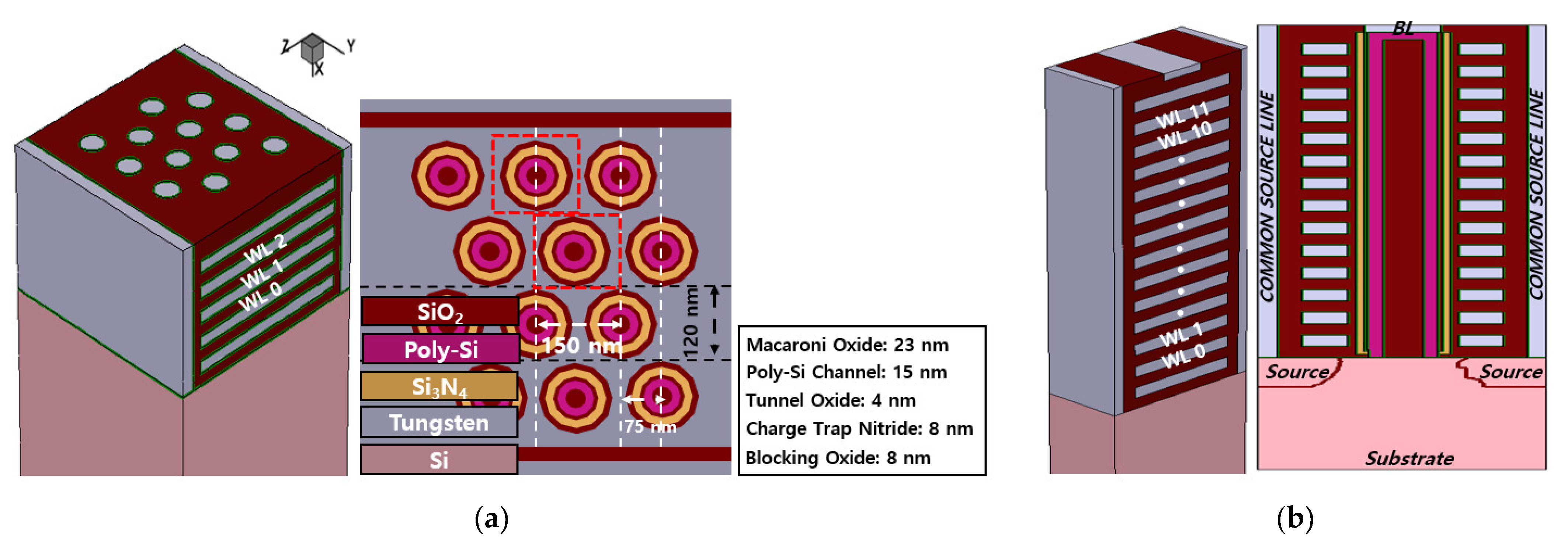
The simulations were conducted on two types of 3D NAND structures to investigate the residual stress of films and the stress-induced effects on the electrical characteristics, respectively, and to minimize simulation time. Figure 1a shows the structural and stack details of the 3D NAND device for stress analysis simulation. Twelve strings, with each string comprising 3 WLs with a string select line (SSL) and a ground select line (GSL), were considered. The diameter of the vertical hole was 120 nm with 150 nm of cell string pitch. Two strings along with the red square dotted box were selected for the stress simulation in order to investigate the position of strings relative to the common source line. The string located near the center and the common source line of 3D NAND will be called the center and slit string, respectively. The structure for the stress-induced effects simulation consisted of 12 WLs, as shown in Figure 1b. The thickness of the macaroni oxide, polysilicon channel, tunnel oxide, charge trap nitride, and blocking oxide were identical for both structures.
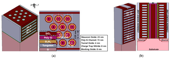
Figure 1.
3D NAND model used for stress simulation and material parameters. 3D simulation model of 3D NAND used in (a) the stress simulation and (b) the stress-induced electrical characteristics variation simulation.
To accurately analyze the impact of scaling on the residual stress of films, the internal stress of tungsten films was tuned to match the industrial devices. As shown in Figure 2a, the residual stress of the tungsten films after the tungsten replacement gate process was approximately 2.41 GPa, which matches reported experimental data [9]. The residual stress of the polysilicon channel at the final structure in the simulation, as shown in Figure 2b, was −280 MPa, which is also similar to the reported data [10]. The distribution of the residual stress of the polysilicon channel in 3D NAND was then analyzed when scaled. The residual stress was calculated using the Maxwell model, which takes dilatational and deviatoric stress into consideration [11]. The mechanical parameters used in this study are summarized in Table 1.
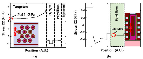
Figure 2.
TCAD calibration with the reported experimental data. The residual stress of (a) the tungsten film after the tungsten replacement gate process and (b) the polysilicon channel in the final structure.

Table 1.
Mechanical parameters used in the 3D NAND simulation. The Young’s modulus (YM), bulk modulus (BM), shear modulus (SM), Poisson’s ratio (PR), and coefficient of thermal expansion (CTE) were used to calculate the mechanical stress simulation.
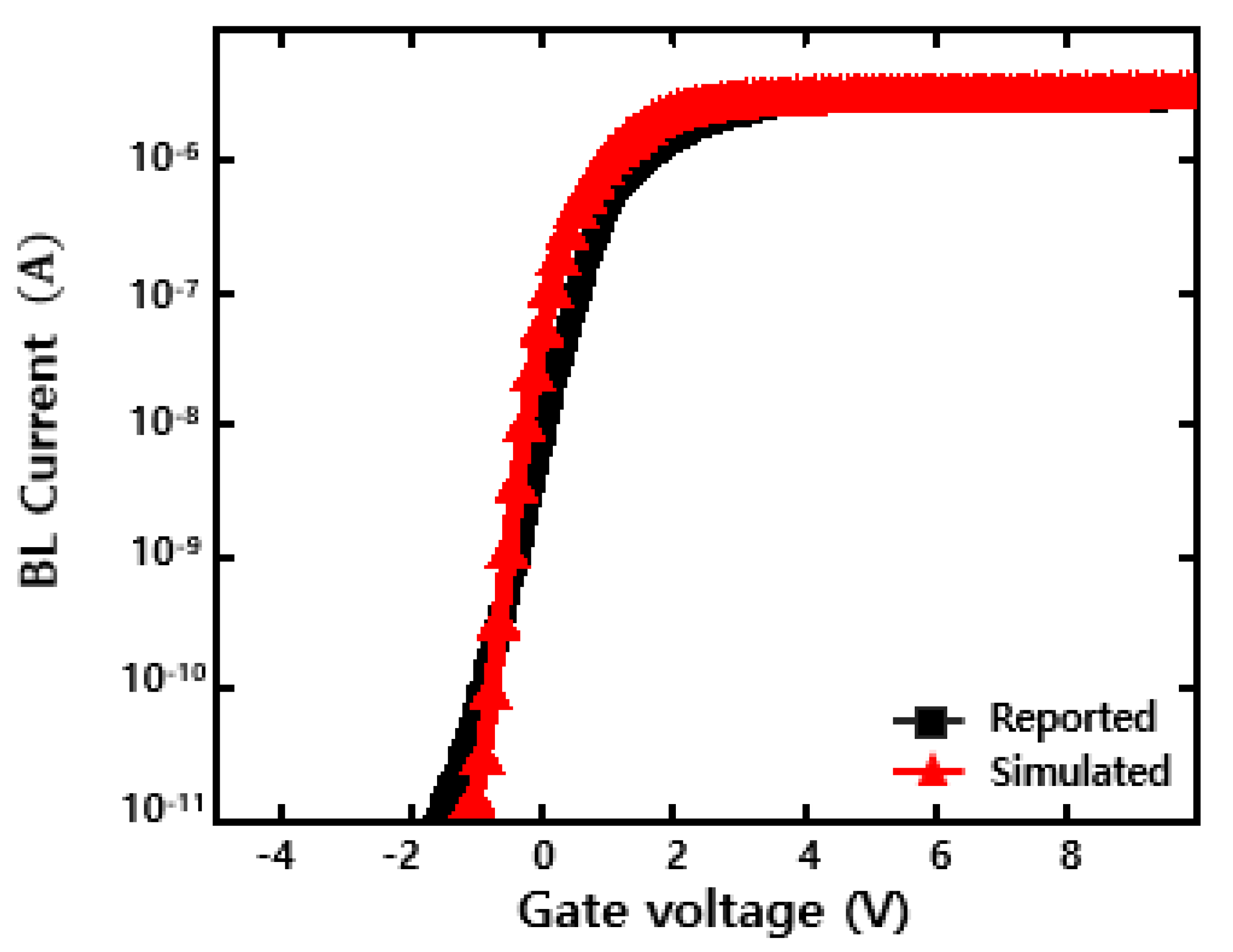
To accurately investigate the impact of residual stress on the electrical characteristics, the BL current and threshold voltage were calibrated by tuning the doping and interface trap parameters of polysilicon to match the reported data, as shown in Figure 3 [12]. Moreover, the deformation potential (minimum, ekp, and hkp) and subband (doping, effective mass, and scattering) model were incorporated in the TCAD device simulations.

Figure 3.
TCAD calibration for the initial state Id-Vg characteristics of the memory transistor with the reported data [12].
3. Results and Discussion
Impact of Scaling on the Residual Stress of the Polysilicon Channel
The residual stress of the polysilicon channel in two strings was considered for analyzing the impact of tungsten films in a common source line. As shown in Figure 4a, the polysilicon channel in the string closest to the common source line had greater compressive residual stress than that in the string closest to the center. When the thickness of the spacer oxide was scaled from 30 nm to 25 nm and 19 nm, with the hole diameter fixed to 120 nm, the channel stress increased in the compressive direction due to the adjacent tungsten gates, which had greater tensile stress than the other films because of their proximity [7]. When the hole diameter was scaled from 120 nm to 100 nm by 10 nm, with the spacer thickness fixed to 30 nm, the channel stress was also increased during compression because of the increase in volume of the tungsten gates surrounding the hole. Figure 4b shows the channel stress when the spacer thickness and hole diameter were both scaled. The channel stress nearly doubled during compression from −260 MPa to −620 MPa in the string closest to center, and from −340 MPa to −660 MPa in the string closest to the common source line, when scaled.
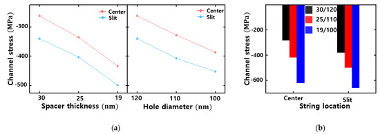
Figure 4.
The channel stress of the two strings with respect to the distance from the common source line. The channel stress of two strings when the spacer thickness and hole diameter were (a) individually scaled and (b) both scaled.
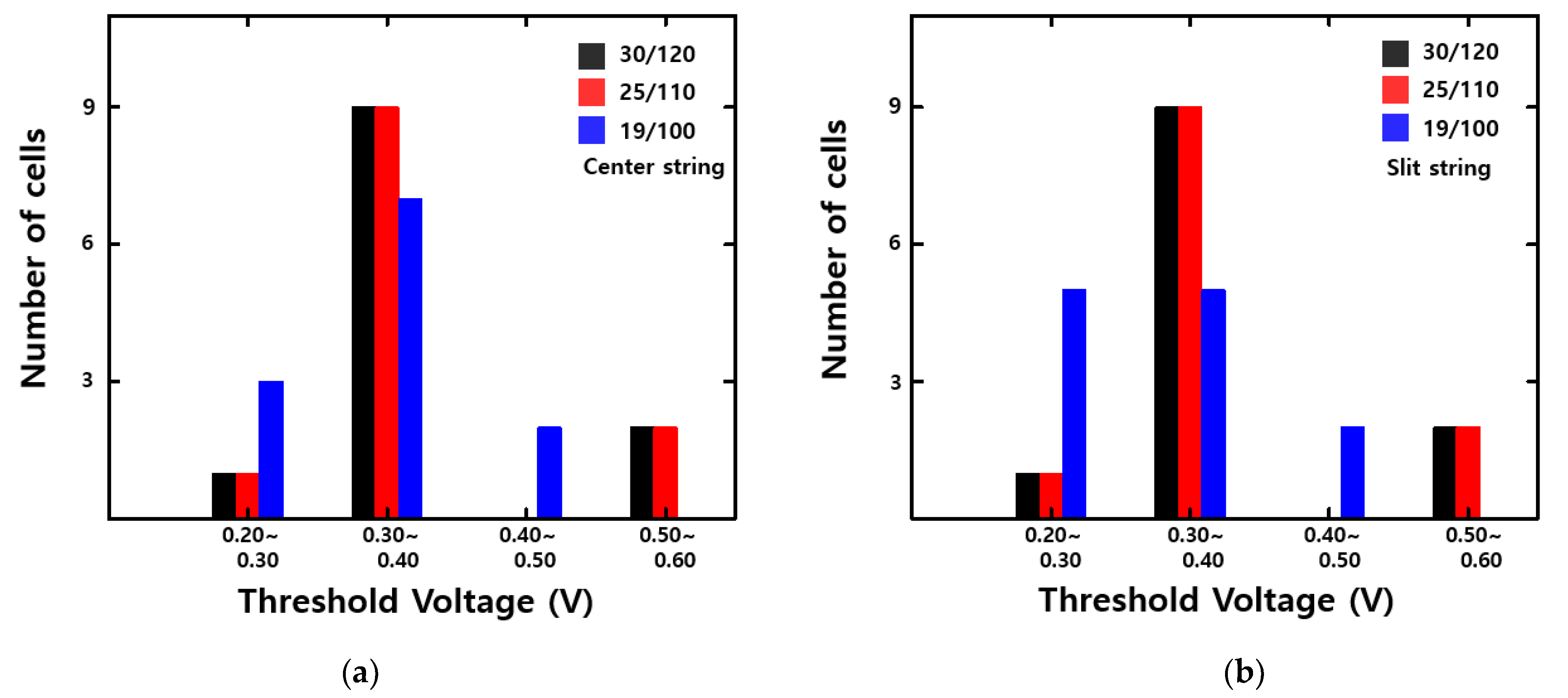
Electrical characteristics, such as BL current (Ion) and threshold voltage (Vth), are affected by the residual stress of the channel region in 3D NAND [13,14]. The compressive channel stress decreases the Ion value due to the degradation of electron mobility caused by the piezo-resistance effect [15]. Furthermore, Vth is negatively shifted, with increasing compressive channel stress due to the lowering of the conduction band [16,17]. The electrical characteristics of the scaled structure are affected by the stress factors and scaling factors. To analyze the impact of only the stress factors, the structure shown in Figure 1b was used, and the residual stress of the polysilicon channel was modulated by depositing tungsten film with different internal stresses to match the simulation data of the channel stress shown in Figure 4b. The BL current and threshold voltage were measured on WL5. Figure 5 presents the BL current and threshold voltage as a function of spacer thickness and hole diameter with the string location. As shown in Figure 5a, the BL current of the string located near the center degraded from 1.84 μA to 1.44 μA and 1.03 μA, with scaling. Moreover, the BL current of the string located near the slit deteriorated from 1.57 μA to 1.32 μA and 0.98 μA. The degradation of the BL current in the two studied strings was attributed to the deterioration of electron mobility caused by increased compressive residual channel stress with scaling [18]. The threshold voltage was shifted negatively in both strings with scaling, as shown in Figure 5b, which can be attributed to conduction band lowering due to the increased channel compressive stress. Therefore, the scaling of the spacer thickness and hole diameter deteriorates the BL current and negatively shifts the threshold voltage of 3D NAND. Figure 6 shows the histogram of threshold voltage of cells in the string located near the center and common source line. When the spacer thickness and hole diameter were scaled to 25 nm and 110 nm, the distribution of the threshold voltages of cells showed no change on either string. However, the negative shift of threshold voltage distribution occurred on both strings by the scaling of spacer thickness and hole diameter to 19 nm and 100 nm, respectively.
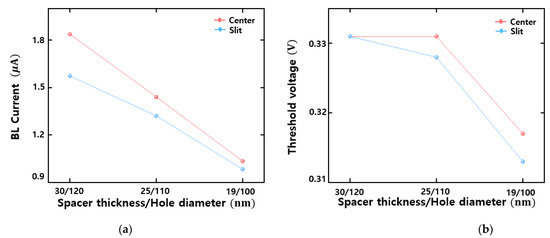
Figure 5.
(a) BL current and (b) threshold voltage of two strings on WL5 when the spacer thickness and hole diameter are both scaled.
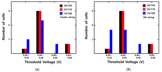
Figure 6.
Distribution of initial threshold voltages of cells when the spacer thickness and hole diameter are both scaled on the string located near the (a) center and (b) common source line.
4. Conclusions
The impact of scaling on the residual stress of a polysilicon channel on two strings in 3D NAND was investigated using TCAD simulation. When the spacer thickness and hole diameter were scaled, the residual polysilicon channel stress was increased during compression, causing detrimental effects to the electrical characteristics. Moreover, the polysilicon channel stress of the string located closer to the common source line was greater than that of the string located closer to center. Compressive residual channel stress degraded the BL current due to the deterioration of electron mobility, and a negative shift of Vth was induced because of the reduced conduction band energy of the polysilicon channel.
This study implies that the residual compressive stress of tungsten must be controlled to prevent degradation of the BL current and the negative shift of the threshold voltage. Further studies are necessary for investigating the impact of stress-induced channel residual stress on the memory characteristics of 3D NAND.
Author Contributions
Conceptualization, J.L., J.-M.S. and D.-G.Y.; methodology, J.L., J.-M.S. and D.-G.Y.; software, J.L. and D.-G.Y.; validation, J.L.; formal analysis, J.L.; investigation, J.L. and D.-G.Y.; resources, J.L. and D.-G.Y.; data curation, J.L. and D.-G.Y.; writing—original draft preparation, J.L.; writing—review and editing, Y.-H.S.; visualization, J.L. and D.-G.Y.; supervision, Y.-H.S.; project administration, J.L.; funding acquisition, Y.-H.S. All authors have read and agreed to the published version of the manuscript.
Funding
This research was supported by Samsung Electronics Co., Ltd., and was also supported by the Ministry of Trade, Industry & Energy (MOTIE (project number 20003808 and project number 10080625)) and Korea Semiconductor Research Consortium (KSRC) support program for the development of the future semiconductor device.
Acknowledgments
The authors would like to thank Lee, J. K. and Lim, J. H. at the Memory Division, Memory R&D Center, Samsung Electronics Co., Ltd., Hwaseong, South Korea, for their technical advice and feedback with regards to this paper.
Conflicts of Interest
The authors declare no conflict of interest.
References
- Siau, C.; Kim, K.H.; Lee, S.; Isobe, K.; Shibata, N.; Verma, K.; Ariki, T.; Li, J.; Yuh, J.; Amarnath, A.; et al. 13.5 A 512Gb 3-bit/Cell 3D Flash Memory on 128-Wordline-Layer with 132 MB/s Write Performance Featuring Circuit-Under-Array Technology. In Proceedings of the 2019 IEEE International Solid-State Circuits Conference—(ISSCC), San Francisco, CA, USA, 17–21 February 2019; pp. 218–220. [Google Scholar]
- Goda, A. 3-D NAND Technology Achievements and Future Scaling Perspectives. IEEE Trans. Electron Devices 2020, 67, 1373–1381. [Google Scholar] [CrossRef]
- Kim, H.; Ahn, S.; Shin, Y.G.; Lee, K.; Jung, E. Evolution of NAND Flash Memory: From 2D to 3D as a Storage Market Leader. In Proceedings of the 2017 IEEE International Memory Workshop (IMW), Monterey, CA, USA, 14–17 May 2017; pp. 1–4. [Google Scholar]
- Parat, K.; Goda, A. Scaling Trends in NAND Flash. In Proceedings of the 2018 IEEE International Electron Devices Meeting (IEDM), San Francisco, CA, USA, 1–5 December 2018; pp. 2.1.1–2.1.4. [Google Scholar]
- Lee, S. Technology scaling challenges and opportunities of memory devices. In Proceedings of the 2016 IEEE International Electron Devices Meeting (IEDM), San Francisco, CA, USA, 3–7 December 2016; pp. 1.1.1–1.1.8. [Google Scholar]
- Kim, J.H.; Lim, J.; Kim, H.S.; Cho, E.S.; Yeo, C.; Lee, W.; You, B.; Lee, B.; Kang, M.; Jang, W.; et al. Highly Manufacturable 7th Generation 3D NAND Flash Memory with COP structure and Double Stack Process. In Proceedings of the 2021 VLSI Symposium Technology, Kyoto, Japan, 13–19 June 2021. [Google Scholar]
- Namkoong, Y.; Yang, H.J.; Song, Y.H. Mechanical Stress Distribution and the Effects of Process Parameter Changes in Vertical NAND Flash Memory. J. Nanosci. Nanotechnol. 2017, 17, 5055–5060. [Google Scholar] [CrossRef]
- Oh, Y.; Sim, J.; Kino, H.; Kim, D.; Tanaka, T.; Song, Y. The Effect of Tungsten Volume on Residual Stress and Cell Characteristics in MONOS. IEEE J. Electron Devices Soc. 2019, 7, 382–387. [Google Scholar] [CrossRef]
- Luoh, T.; Huang, Y.; Chen, C.; Hung, Y.; Yang, L.; Yang, T.; Chen, K. Tungsten Gate Replacement Process Optimization in 3D NAND Memory. In Proceedings of the 2019 Joint International Symposium on e-Manufacturing & Design Collaboration(eMDC) & Semiconductor Manufacturing (ISSM), Hsinchu, Taiwan, 6 September 2019; pp. 1–4. [Google Scholar]
- Kruv, A.; Arreghini, A.; Verreck, D.; Gonzalez, M.; Bosch, G.V.D.; Wolf, I.D.; Rosmeulen, M. Impact of Mechanical Stress on 3-D NAND Flash Current Conduction. IEEE Trans. Electron Devices 2020, 67, 4891–4896. [Google Scholar] [CrossRef]
- Roylance, D. Engineering Viscoelasticity; Massachusetts Institute of Technology: Cambridge, MA, USA, 2001. [Google Scholar]
- Bhatt, U.M.; Manhas, S.K.; Kumar, A.; Pakala, M.; Yieh, E. Mitigating the Impact of Channel Tapering in Vertical Channel 3-D NAND. IEEE Trans. Electron Devices 2020, 67, 929–936. [Google Scholar] [CrossRef]
- Shimizu, A.; Hachimine, K.; Ohki, N.; Ohta, H.; Koguchi, M.; Nonaka, Y.; Sato, H.; Ootsuka, F. Local mechanical-stress control (LMC): A new technique for CMOS-performance enhancement. In Proceedings of the International Electron Devices Meeting, Technical Digest (Cat. No.01CH37224), Washington, DC, USA, 2–5 December 2001; pp. 19.4.1–19.4.4. [Google Scholar]
- Kruv, A.; Arreghini, A.; Gonzalez, M.; Verreck, D.; Bosch, G.V.D.; Wolf, I.D.; Furnémont, A. Impact of Mechanical Stress on the Electrical Performance of 3D NAND. In Proceedings of the 2019 IEEE International Reliability Physics Symposium (IRPS), Monterey, CA, USA, 31 March–4 April 2019; pp. 1–5. [Google Scholar]
- Ito, S.; Namba, H.; Yamaguchi, K.; Hirata, T.; Ando, K.; Koyama, S.; Kuroki, S.; Ikezawa, N.; Suzuki, T.; Saitoh, T.; et al. Mechanical stress effect of etch-stop nitride and its impact on deep submicron transistor design. In Proceedings of the International Electron Devices Meeting 2000, Technical Digest. IEDM (Cat. No.00CH37138), San Francisco, CA, USA, 10–13 December 2000; pp. 247–250. [Google Scholar]
- Weimin, Z.; Fossum, J.G. On the threshold Voltage of strained-Si-Si/sub 1-x/Ge/sub x/ MOSFETs. IEEE Trans. Electron Devices 2005, 52, 263–268. [Google Scholar]
- Lim, J.S.; Yang, X.; Nishida, T.; Thompson, S.E. Measurement of conduction band deformation potential constants using gate direct tunneling current in n-type metal oxide semiconductor field effect transistors under mechanical stress. Appl. Phys. Lett. 2006, 89, 73509. [Google Scholar] [CrossRef]
- Smith, C.S. Piezoresistance Effect in Germanium and Silicon. Phys. Rev. 1954, 94, 42–49. [Google Scholar] [CrossRef]


Publisher’s Note: MDPI stays neutral with regard to jurisdictional claims in published maps and institutional affiliations. |
© 2021 by the authors. Licensee MDPI, Basel, Switzerland. This article is an open access article distributed under the terms and conditions of the Creative Commons Attribution (CC BY) license (https://creativecommons.org/licenses/by/4.0/).