Article

Ultra-Wideband Solar Energy Absorption Device Based on Metal–Dielectric Symmetrical Gap Separation


1
School of Electronic Information and Electrical Engineering, Chengdu University, Chengdu 610106, China
2
China Coal Technology & Engineering Group, Chongqing Research Institute Co., Ltd., Chongqing 401332, China
3
College of Physics & Information Engineering, Quanzhou Normal University, Quanzhou 362000, China
4
School of Mathematics and Physics, Southwest University of Science and Technology, Mianyang 621010, China
5
School of Chemistry and Chemical Engineering, Jishou University, Jishou 416000, China
*
Authors to whom correspondence should be addressed.
Coatings 2026, 16(2), 211; https://doi.org/10.3390/coatings16020211
Submission received: 22 December 2025 / Revised: 4 February 2026 / Accepted: 4 February 2026 / Published: 6 February 2026

Abstract

Solar energy stands as one of the most promising green energy sources today. This paper proposes a symmetrical gap-type separated solar absorber and radiator (SETR) featuring a dielectric layer of Al2O3 and metal W as separation columns. Its unique structure enhances absorption within the effective solar energy spectrum, thereby alleviating solar energy absorption challenges. The finite difference time domain method (FDTD) results show that the SETR achieves an absorption rate of more than 90% in the 280–2096 nm band, which perfectly covers the visible light band range. The weighted average absorption in the 280–2500 nm band is 95.22% under AM1.5 conditions. The thermal emission efficiency at 1500 K is 95.13%, and the thermal radiation loss is less than 5%. Beyond analyzing the results, we also investigated the overall band absorption efficiency of the SETR under varying conditions by adjusting its structural parameters and physical parameters such as materials. This approach enables effective control over the absorption spectrum. Additionally, the proposed SETR is independent of polarization conditions. Both the TM and TE modes are insensitive to large incident angles. In the future, broadband SETRs can be applied to solar energy harvesting, thermoelectric conversion, and imaging fields, as it holds broad application prospects.

1. Introduction

Traditional fossil energy is the main energy source today, but its non-renewable nature cannot meet the future energy needs of human beings [1]. As a kind of non-fossil energy with huge reserves and almost zero pollution, solar energy has been widely used in photovoltaic power generation, thermochemical conversion and photocatalysis in recent years [2,3,4,5]. However, it is still one of the core challenges to efficiently capture solar energy and convert it into other energy [6]. In addition,, efficient energy conversion remains one of the core challenges in converter devices [7]. Current common energy conversion applications include perovskite batteries, steam turbines, and endothermic towers [8,9]. Among them, solar absorbers are becoming more popular. This is because they can capture light efficiently and their structure is flexible. However, numerous challenges persist in research, such as low absorption efficiency and instability under high-angle solar incidence [10,11]. Therefore, the key to maximizing solar energy utilization lies in designing solar absorbers that combine high efficiency with broad bandwidth characteristics.
Metamaterials are artificial composite materials [12,13], which have been widely used in the regulation of multiple wavelength bands, high-efficiency absorption, device heat dissipation and electromagnetic stealth [14,15,16]. Since the concept of a metamaterial absorber was proposed by Landy et al. [17] in 2008, absorbers based on metamaterial designs have achieved excellent absorption performance in the visible [18], mid-infrared [19] and terahertz [20]. Therefore, the enhancement of solar absorber performance primarily focuses on the design of various types of metamaterials [21,22,23]. In 2022, Zhou et al. [24] designed an ultra-wideband perfect absorber based on four different material structures of silicon nitride-titanium-silicon nitride-titanium. This multilayer material combination yielded favorable results in the absorption spectrum. In the same year, Liang et al. [25] adopted a metal–dielectric–metal structure to realize the multi-band absorption switching of the perfect absorber at a nearly 100% absorption rate by adjusting the silver disk array. In 2023, Gao et al. [26] designed a square ring structure based on TiN to achieve high absorptivity, good spectral selectivity and thermal tolerance of the absorber in the main solar spectral region. Because of its TiN as a high-performance refractory material [27], the absorber can maintain more than 80% of the solar heat conversion efficiency at 700 °C.
On the other hand, it has been found in the research process that the absorber material will produce plasma resonance when capturing the incident light, which is the mechanism for the absorber to achieve broadband absorption [28,29,30]. The intensity of the resonance phenomenon mainly depends on the structure of the absorber. In 2020, Yue et al. [31] designed a zigzag and pyramid-shaped multilayer absorber structure. The multiple slow light modes between the layers and the plasma resonance coupling are the working principles of its broadband absorption. Zhou et al. [32] verified the Ti-Ge-Ti three-layer absorber structure in 2021. In the air groove area of the Ti upper structure, the surface plasmon resonance phenomenon is strong.
Through the aforementioned preliminary research, the solar absorber and thermal radiator (SETR) structure designed in this paper overcomes the inherent limitations of single-precious-metal systems. By continuously combining and optimizing various conventional geometric configurations—including rectangular films, disks, and ellipsoidal films—the resulting SETR structure enhances the synergistic regulation between the dielectric layer and the metal layer. This creates a composite cavity that captures greater amounts of sunlight. Consequently, a symmetric gap-type split SETR structure is designed, utilizing Al2O3 as the dielectric layer and W as the metal layer to serve as separation pillars. It is evident that the distinctive configuration of the system under consideration has been meticulously engineered to ensure optimal performance in terms of the simulation results. The equidistant gap in the split column can well generate the phenomenon of surface plasmon resonance, thereby achieving broadband absorption effect. The results show that the designed SETR achieves a bandwidth of more than 90% in the 1816 nm band, and the weighted average absorption is 95.22% in the 280–2500 nm band under AM1.5 conditions. Compared with other solar absorbers, this structure has comprehensive advantages in thermal stability, polarization independence, wide spectral-response range and high wide-angle absorption efficiency. Based on these characteristics, the broadband wide-angle SETR is suitable for solar energy collection systems and infrared thermal imaging devices. Its multilayer design achieves efficient photothermal conversion by regulating the photon localization effect, and can be extended to the photovoltaic field to improve spectral utilization.

2. Structural Parameters of the SETR

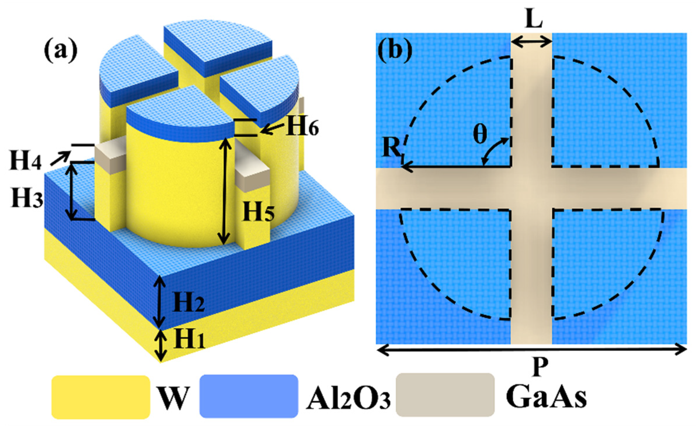
We propose a symmetrical gap-separation-structure design based on an alumina dielectric layer and a metallic tungsten cylinder, utilizing FDTD principles [33,34,35]. In the FDTD Solutions software(Lumerical FDTD 2023 R2.3) analysis, incident sunlight on the SETR is modeled as a plane wave with a wavelength range spanning 280 to 3000 nm, covering ultraviolet, visible, near-infrared, and mid-infrared bands. Periodic boundary conditions are applied in the X and Y directions to simulate the regular arrangement of SETRs along these axes, accommodating the incident plane sunlight [36]. A perfect matching layer (PML) is implemented in the Z direction to prevent reflected light from interfering with SETR absorption, thereby achieving low reflection absorption [37,38]. Transmission and reflection monitors are positioned below and above the SETR, respectively. As shown in Figure 1a below, the bottom is a substrate consisting of oriented thin-film W with Al2O3 and the top consists of two parts, one is a symmetric gap-separated cleavage column consisting of Al2O3-W, and the other is a cross-shaped rectangular structure consisting of GaAs-W to fill the gap of the cylindrical separation, and they have the thickness parameters of H1 = 100 nm, H2 = 170 nm, H3 = 180 nm, H4 = 50 nm, H5 = 330 nm, and H6 = 50 nm. The top view of the SETR is shown in Figure 1b, from which it can be seen that the width of the gap L = 80 nm, the radius of the cylinder R = 210 nm, θ = 90°, the structural period of the individual SETR P = 600 nm, and the dielectric constants of the materials used in the SETR are all derived from Palik [39].
During the manufacturing process of solar absorbers, the substrate is first cleaned with acetone, alcohol, and deionized water. After the substrate is air-dried, the experimental manufacturing phase begins. The first step involves depositing a 100-nanometer-thick tungsten film onto the tungsten substrate using magnetron sputtering technology [40]. Subsequently, ion beam sputtering is employed to sequentially deposit a composite film sequence of Al2O3 (170 nm)—W (180 nm)—GaAs (50 nm)—W (330 nm)—Al2O3 (50 nm) onto the tungsten surface. The second step utilizes photolithography and electron beam evaporation to fabricate the required microstructures [41]. Finally, a symmetric gap-separated structure array was deposited through standard photolithography processes—including coating, pre-drying, exposure, development, curing, electron beam lithography, and photoresist stripping [42]. This structure exhibits ultra-thin characteristics. Although device dimensions pose manufacturing challenges, this approach offers novel insights for solar absorber design. The current process is feasible and holds promise for low-cost mass production in the near future.

3. Result and Discussion

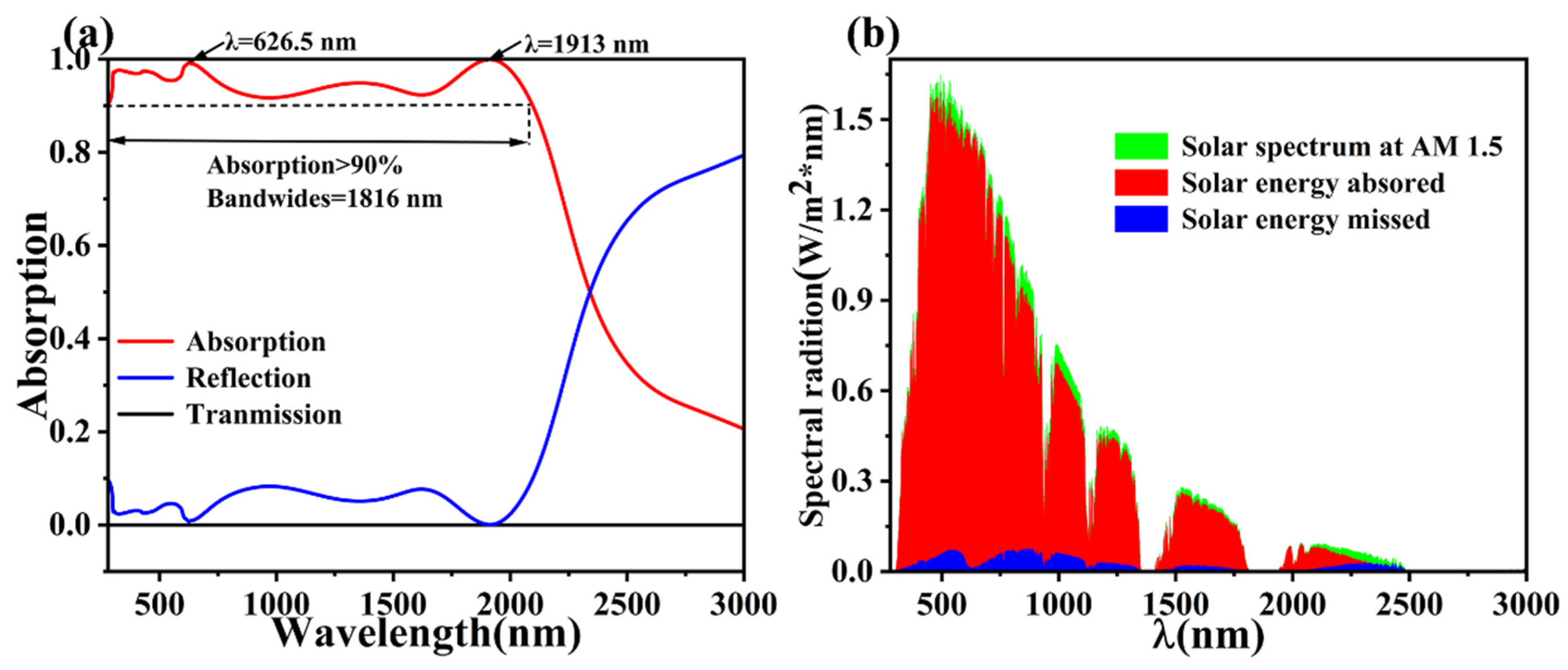
We calculated the spectral reflection efficiency (R) and the spectral transmission efficiency (T) of the SETR, and since our metal tungsten at the bottom is an opaque metal and the thickness is thick enough, we can consider that the transmission of the light through the SETR is zero, and the SETR’s overall band absorption efficiency (280–3000 nm) was then calculated using the following formula: A = 1 − R − T [43,44,45]. As shown in Figure 2a, the absorption realizes a broadband absorption of 1816 nm (280–2096 nm) band range with greater than 90% broadband absorption, where two absorption peaks, localized at λ = 626.5 nm and 1913 nm, respectively, are achieved, reaching more than 99%. Because the Earth’s atmosphere scatters, reflects, and absorbs solar radiation, we introduce atmospheric mass to describe solar radiation traveling through it. We define the global spectral equation for incident solar energy at AM1.5 as Formula (1) [46]:
η A = λ M i n λ M a x A ( ω ) I A M 1.5 ( ω ) d ω λ M i n λ M a x I A M 1.5 ( ω ) d ω
When the SETR is in the ideal AM1.5 solar spectrum, as shown in Figure 2b, which shows the spectral absorption and loss energy of the SETR under AM1.5, where the blue region is the energy lost by the SETR, the red region is the energy absorbed by the SETR, and the green region is the energy radiated by the sun under the AM1.5 condition, it can be observed that the loss of energy is mainly centered at 500–622 nm, 750–1100 nm and 2200–2400 nm. It can be calculated that the weighted average absorption under visible light (380–750 nm) is 96.96%, and the loss is less than 5%, which is a very good result. For the wavelength range (280–2500 nm) where the solar radiation energy is mainly concentrated, the weighted average absorption of the SETR is 95.22%. For the wavelength range (280–2500 nm) where the solar radiation energy is mainly concentrated, the SETR has a weighted average absorption of 95.22%, which also has good absorption performance.
Figure 2. (a) Absorption, reflection and transmission efficiencies of the SETR under planar sunlight; (b) spectral absorption and loss energy of the SETR at AM1.5.
Coatings 16 00211 g002
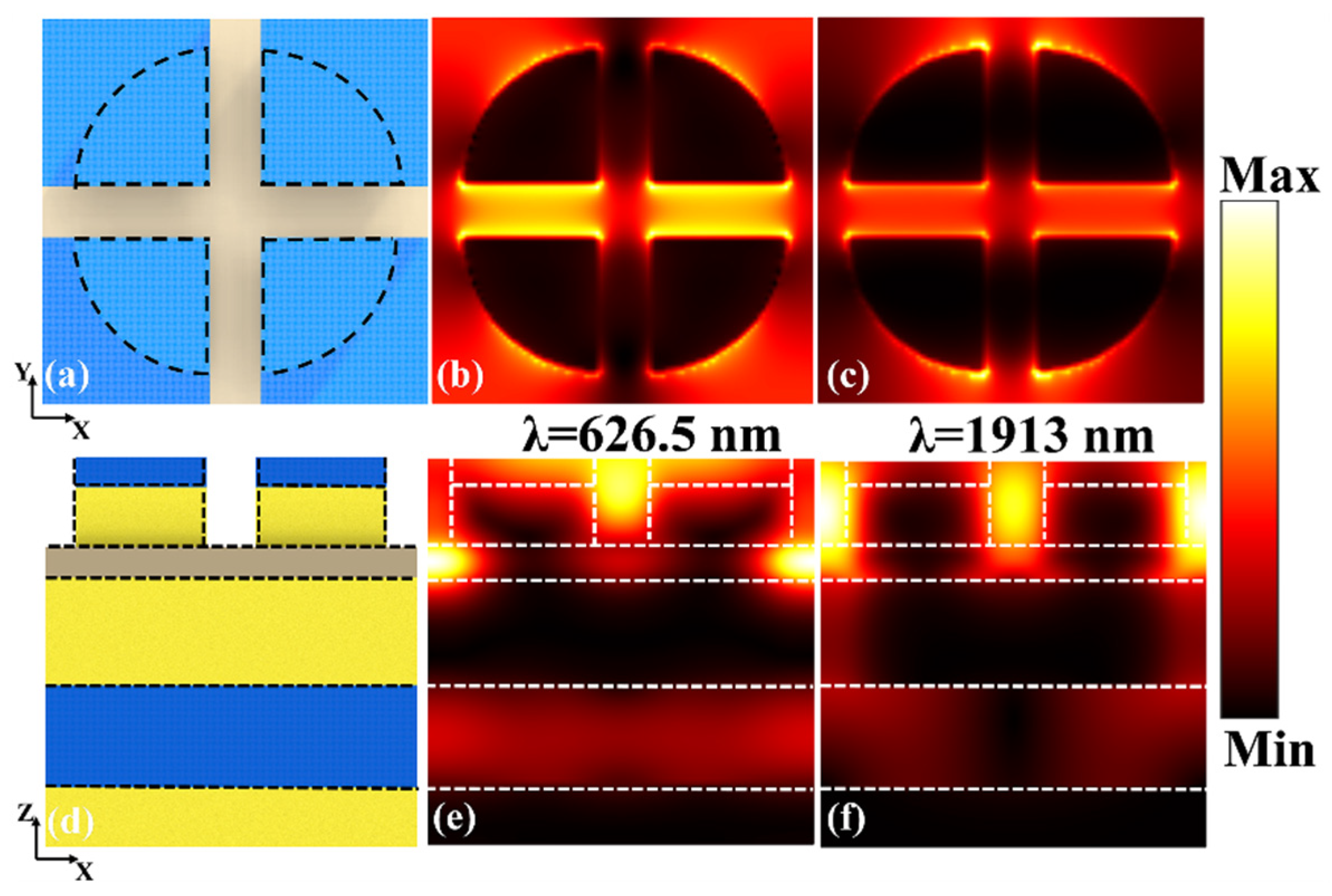
After obtaining the two absorption peaks, λ = 626.5 nm and 1913 nm, from the absorption efficiency diagram, in order to further analyze the physical mechanism of the SETR to produce perfect absorption in the visible to near-infrared wavelength bands [47,48,49], we give the electric field distribution diagrams of the SETR in the XOY as well as the XOZ directions at 626.5 nm and 1913 nm. As demonstrated in Figure 3a,d, the structural view of the SETR in the XOY direction and the sectional view of the center in the XOZ direction, respectively, facilitate the observation and comparison of the intensity of the electric field distribution of the SETR in each layer of the film system. At a wavelength of 626.5 nm, as shown in Figure 3b,e, the bright spots on the surface are mostly in the space between the separating cylinder and the cross-shaped corner of the rectangular thin-film GaAs, with the incidence of planar sunlight, after passing through the interior of the bottom square thin-film Al2O3, it is finally completely reflected by the bottommost opaque metal W and no longer propagates downward. When the wavelength increases to 1913 nm, as shown in Figure 3c,f, the surface iso-polarized excitations further propagate toward the bottom of the gap and cause the vibration of the localized surface iso-polarized excitations on the surfaces of the cracked columns and the cross-shaped rectangles, and the integrated SETR’s absorption efficiency graphs tell us that the absorption decreases very quickly after 1913 nm, so that this phenomenon of electric field enhancement does not last for a long time [50]. In conclusion, the efficient absorption of our designed SETR cannot be separated from the symmetric gap structure of the split column, which can concentrate the electric field well in the visible to near- and mid-infrared wavelength ranges, and it is more convenient to regulate the surface-isolated exciton resonance phenomenon of the SETR.
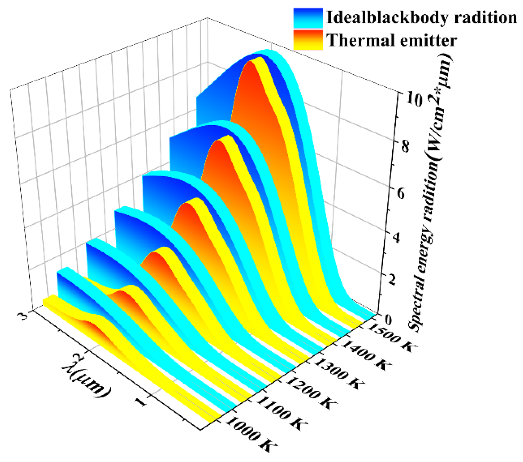
In order to better observe the extent to which the actual SETR emission approaches the blackbody radiation, we investigated the variation in the energy emission of the SETR over the temperature range from 1000 K to 1500 K over the entire band. We also define a key parameter of the emitter as thermal emission efficiency (ε, calculated using Formula (2) [51]:
ε = λ M i n λ M a x ε ( ω ) · I B E ( ω , T ) d ω λ M i n λ M a x I B E ( ω , T ) d ω
The temperatures of 1000 K, 1100 K, 1200 K, 1300 K, 1400 K, and 1500 K are simulated as shown in Figure 4, where the blue gradient region is the energy radiated by the blackbody model in the ideal case, while the red gradient region is the emission from the actual SETR, and in the three-dimensional plots, we can intuitively observe the degree of closeness of the two models. As the temperature increases, the emission energy increases as a whole, while the maximum value of the emission is shifted towards shorter wavelengths with increasing temperature, which is caused by the Wien displacement law for blackbody radiation. For our designed SETR model, the temperature variation range from 1000 K to 1500 K exhibits excellent fit to the ideal case blackbody radiation model in the band range below 1600 nm, showing good emission intensity profiles, while the main emission loss of the SETR occurs in the near- and mid-infrared wavelengths after 2000 nm.
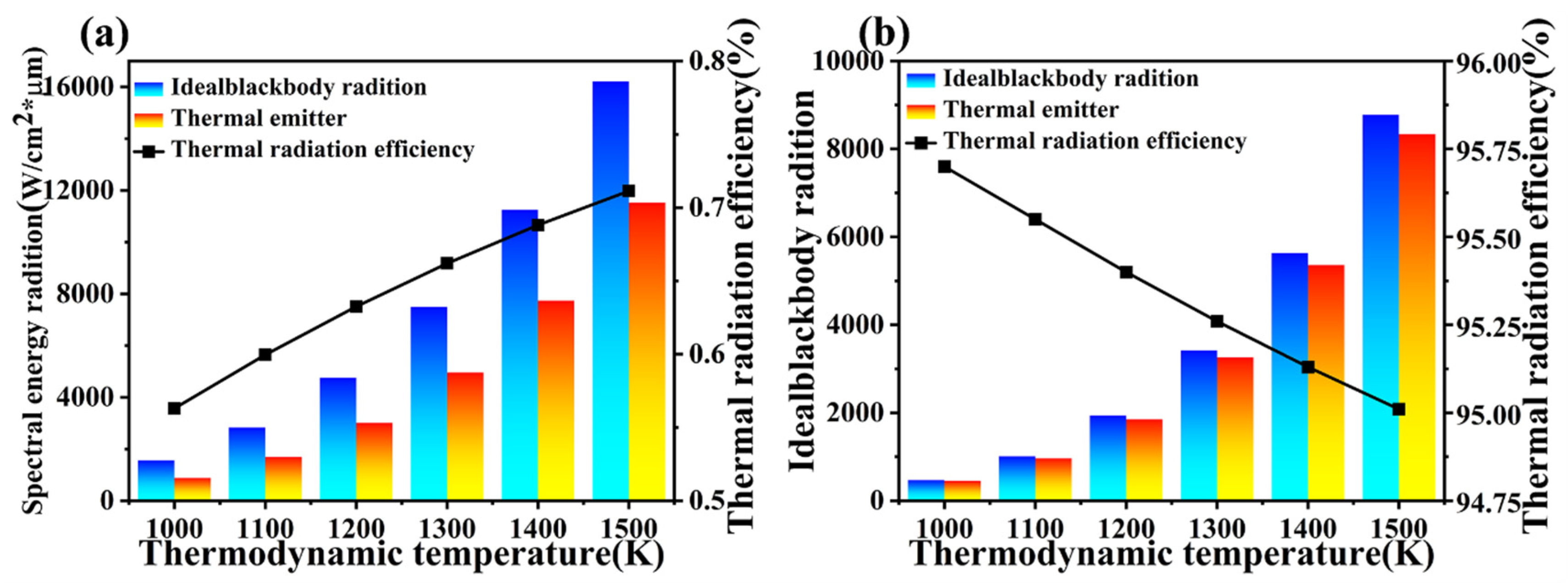
In order to go a step further and make the energy emission intensity analysis accurate, we give a bar-dot line plot of the emission intensity with detailed numerical values to give an explanation. As shown in Figure 5a, the blue bar is the energy radiated by the blackbody model in the ideal case, while the red bar is the emission from the actual SETR, and the height of the bar then represents the total radiated value of the blackbody radiation model and the SETR’s emitted energy for different temperatures in the 280–3000 nm band, while the dotted line curve represents the thermal emission efficiency of the absorber, which is to say, reflecting the SETR’s fitness to the blackbody model’s radiation over the whole waveband. The dotted curve represents the thermal emission efficiency of the SETR, which reflects the degree of fitness between the SETR and the blackbody model radiation in the whole band. It can be observed that as the temperature increases, the thermal emissivity also increases with the increase from about 55% to about 72%, and it is obvious that such a low emissivity is due to the fact that we have taken the band with the largest radiation loss after 2500 nm into account, and for this reason, we further analyze the SETR according to the designed SETR A > 90% of the effective wavelength range (280–2096 nm), which yields the results as shown in Figure 5b, in which the height difference between the blue bar and the red bar is greatly reduced compared with Figure 5a, which also represents that the loss of emission energy of the SETR is also reduced, and the emission efficiencies of the SETR at the six temperatures are 95.7%, 95.55%, 95.4%, 95.26%, 95.13%, and 95.01% in that order, which is a very small change and does not affect the overall excellent emission efficiency.
In Table 1, we can see the advantages of our designed SETR with other absorbers by comparing the SETR models mentioned in other studies [52,53,54,55]. Firstly, in the structure we used a symmetric gap-separated cylinder composed of Al2O3-W and a cross-shaped rectangular structure composed of GaAs-W to fill the gap of the cylindrical separation, which is a very novel structure, and secondly, we used a symmetric gap-separated cylinder composed of Al2O3-W to fill the gap of the cylindrical separation. The average absorption rate of the designed SETR in the bandwidth of 1816 nm reaches 94.99%, and after comparing the weighted average absorption efficiency under AM1.5 and the thermal radiation efficiency, it is concluded that our designed SETR has the advantages of novel structure and good performance, which can have a great potential to be utilized in the field of light absorption.
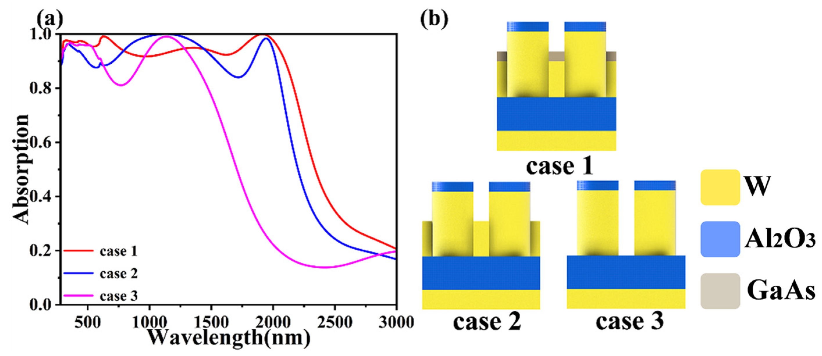
In order to investigate the effect of the cross-shaped rectangular structure on the overall absorption efficiency, we have given three different structures as shown in Figure 6b: case 1 is the model structure of the SETR we designed; in case 2, we removed the GaAs layer of the cross-shaped rectangular structure; and in case 3, we removed the GaAs layer and the W layer of the cross-shaped rectangular structure and retained only the separated cylindrically symmetric gap-type structure. In Figure 6a, it can be observed that case 2, which lost the cross-shaped rectangular structure of the GaAs layer, has a decrease in absorption in the visible wavelength band but makes up for the loss of absorption in the near-infrared wavelength band of 800–1600 nm, although it does not last long, and the absorption decreases with the increase in wavelength just as drastically [56,57]. Meanwhile, when we remove the GaAs layer with the W layer, that is, in case 3, which completely removes the cross-shaped rectangular structure, the absorption is unsatisfactory and the effective bandwidth is too short and unstable to be discussed too much.
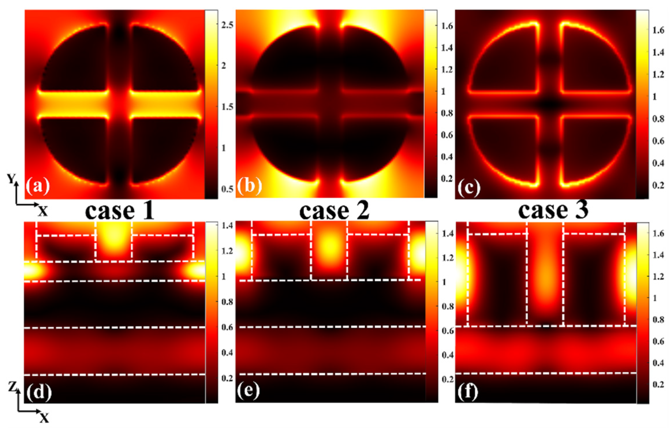
Therefore, in order to analyze the physical mechanism by which the cross-shaped rectangle affects the overall absorption, we give plots of the electric field strengths in the XOY and XOZ directions for case 1, case 2, and case 3 at λ = 626.5 nm, in which the monitors observing the electric field in the XOY direction are placed on the upper surface of the GaAs layer of the cross-shaped rectangle, on the upper surface of the W layer of the cross-shaped rectangle, and on the upper surface of the square thin-film Al2O3 layer, respectively. Upper surface of the W layer of the cross-shaped rectangle and the upper surface of the Al2O3 layer of the square film. As shown in Figure 7a,d, due to the presence of the cross-shaped rectangular structure, which fills the gap of the separated cylinders, the region is well concentrated with surface-isotropic excitations resonating bright spots [58]. When the GaAs layer of the cross-shaped rectangle is removed, as in Figure 7b,e, it can be observed that the surface-isotropic polarized excitations propagate downward with the gap and their intensities decrease, and at the same time, they lose local surface-isotropic excitations from the GaAs layer [59,60]. This is the reason for the low absorption of case 2 in the visible light; when we completely remove the GaAs layer and the W layer of the cross-shaped rectangle, as in Figure 7c,f, we can see that the sunlight does not propagate in the cross-shaped rectangular structure, and the highlights of the surface equipolarized excitations of the intermediate interstitials are further downwardly shifted to the inner part of the underlying thin-film Al2O3 while the phenomenon of the surface equipolarized excitations resonance concentrates in the four symmetric cleavage columns of the surface.
Since the upper part of the SETR consists of two parts, one of which is a slit column with symmetric gap separation composed of Al2O3-W and the other a cross-shaped rectangular structure composed of GaAs-W, which is used to fill the gap of the cylindrical separation, we next discuss the effect of the slit column composed of Al2O3-W on the absorption.
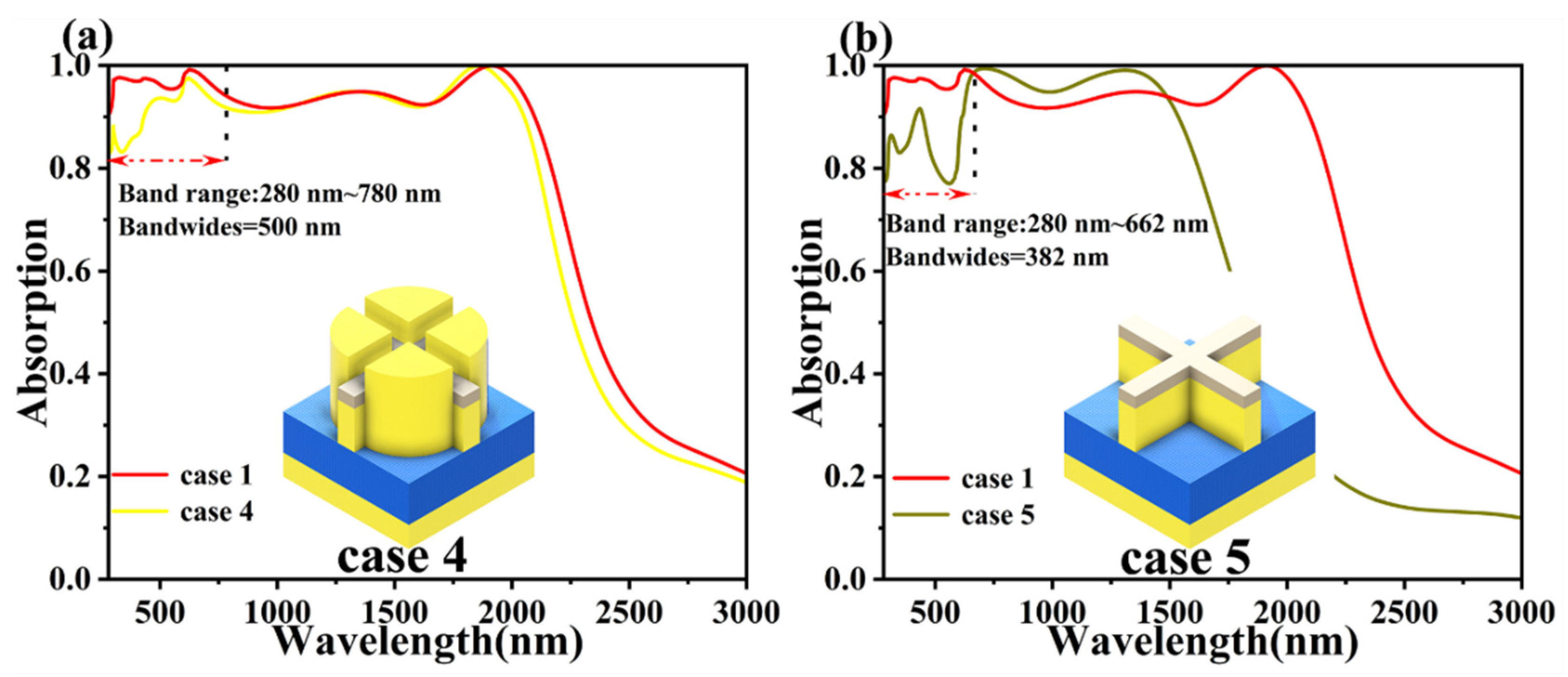
Next, we shall conduct a quantitative analysis of the geometric structure of the SETR. As shown in Figure 8a, case 4 is the model of the SETR with the Al2O3 layer removed from the top of the cracked column, and it can be seen that the absorption curve of case 4 is basically overlapped with that of our case 1 in the near-infrared band after 1000 nm, and the main difference is centered on the 500 nm bandwidth of 280–780 nm, where the absorption of case 4 is not as good as it could be, which shows that our designed Al2O3 dielectric layer can well compensate the SETR in the visible light absorption and also improve the tiny absorption efficiency in the mid-infrared band. As shown in Figure 8b, case 5 is an SETR with the split column completely removed, and only the cross-shaped rectangular structure is retained on the absorbing super-surface, which further shortens the fluctuation bandwidth of the absorption curve, and unstable absorption occurs in the visible range of 280–662 nm, but it can capture the visible and near-infrared light very well in the band of 662–1500 nm as compared with that in case 1, and this can be used for the future improvement in SETR in specific wavelengths in the mid-infrared. This provides a guideline for future improvement in SETR absorption in specific bands [61,62].
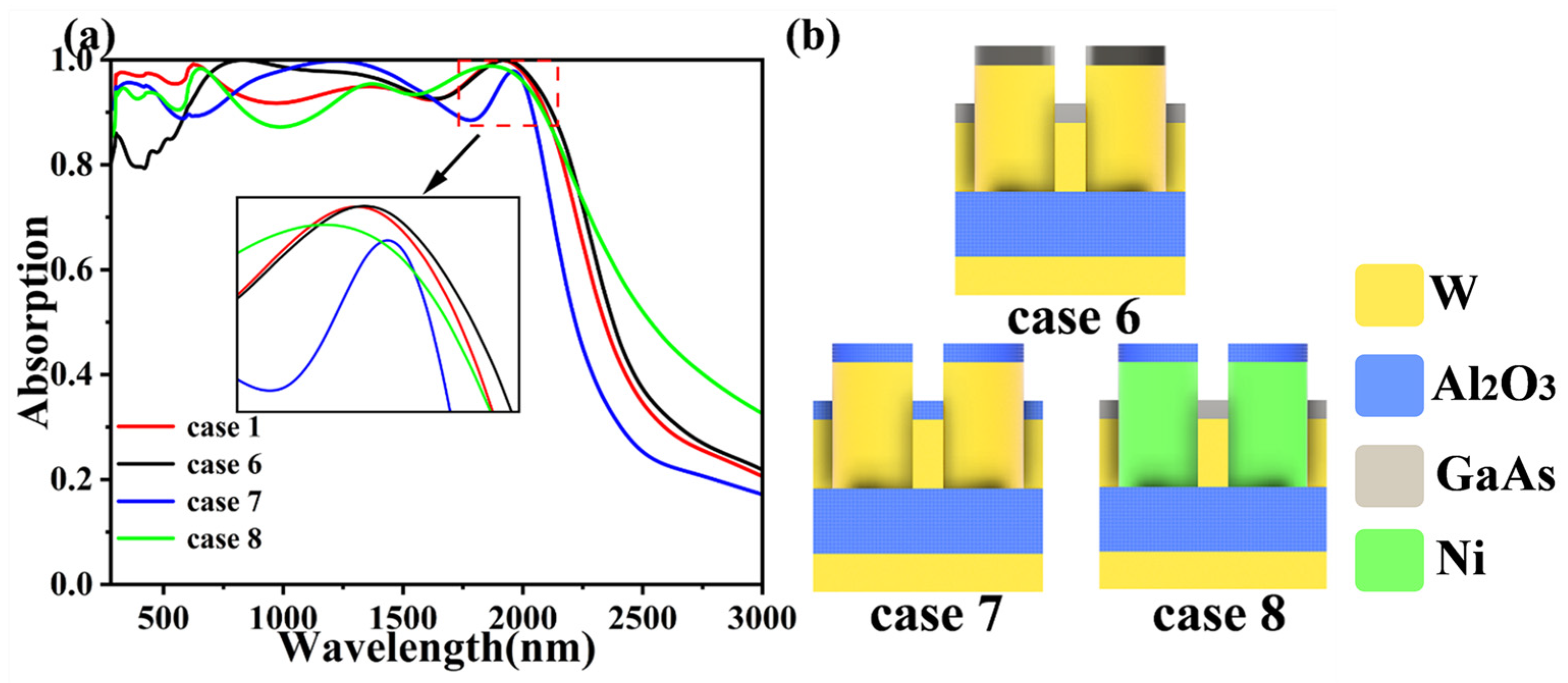
Investigating the impact of different materials on absorption efficiency is central to optimizing SETR performance [63,64]. By altering one material while keeping all other structural components unchanged, we quantitatively analyze the influence of that material on the overall absorption of the SETR. As shown in Figure 9a, in the absorption curves of the SETR after material modification, case 6 in Figure 9b replaces the Al2O3 dielectric layer at the top of the separation column with GaAs. It can be observed that compared to the absorption curve of case 1, its visible light absorption performance is inferior. This result indicates that the dielectric layer design of the separation column is crucial for the overall absorption efficiency of SETR. In case 7, we replaced the GaAs layer at the top of the cross-shaped rectangle with Al2O3. Since no equal-exciton resonance aggregation occurred on the inner surface of the GaAs layer, the absorption curve exhibited significant fluctuations and instability across the entire wavelength range. In contrast, in case 8, replacing the W layer of the splitter column with metallic Ni while maintaining the cross-shaped structure yielded exemplary absorption curves with exceptional trapping capabilities in certain bands compared with case 1.
In the design of nano-sized devices, due to the size sensitivity, small parameter variations can significantly affect the resonance mode and energy absorption mechanism of the SETR [65,66,67]. In order to determine the optimal combination of performance parameters for the design of the SETR, we simulate and analyze the gradient variations in the key structural parameters.
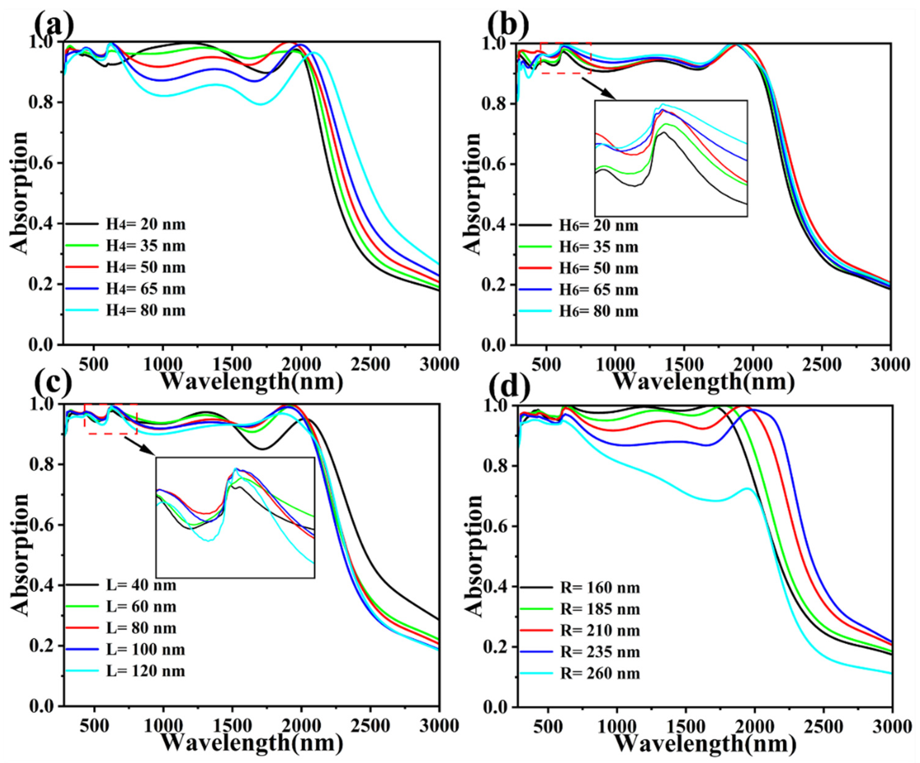
On the other hand, the key geometric parameters of the SETR also exert a significant influence on absorption. Here, we varied the value of one parameter at a time: H4, H6, L, or R while keeping the other parameters constant. As shown in Figure 10a, the absorption spectrum of the gallium arsenide layer at the top of the cross-shaped rectangular structure increases from 20 nm to 80 nm. It can be observed that as the H4 content increases, the SETR absorption in the near-infrared band (800 nm to 2000 nm bandwidth) gradually weakens, while no significant changes occur in the visible light band. This is primarily attributed to the Al2O3 dielectric layer atop the split column effectively compensating for the SETR’s deficiencies in visible light absorption. Consequently, within the H4 gradient ranging from 20 nm to 80 nm, SETR absorption exhibited the greatest stability at H4 = 50 nm, confirming 50 nm as the optimal thickness for the GaAs layer. As shown in Figure 10b. This figure shows the absorption curve of the dielectric layer Al2O3 at the top of the splitter column from 20 nm to 80 nm. Overall, the absorption is difficult to distinguish because we know that Al2O3 mainly influences the visible absorption in the design of the SETR from the previous analysis. For this reason, we have amplified the absorption in the visible band locally, and we can see that the absorption of the SETR in the visible band is not significant [68]. We can also see that the absorption curve at H6 = 50 nm is in the middle, and the absorption in the near the mid-infrared bands are more stable. Next, we will study how the gap width affects the absorption. Next, we investigate the effect of gap width on absorption characteristics. As shown in Figure 10c, the absorption curves are plotted as the gap width varies from 40 nm to 120 nm. Unlike the regular patterns observed for H4 and H6, the variation in L exhibits irregularity: at a gap width of 40 nm, the size is too small for surface polarization to fully propagate. As the gap increases, visible light absorption rises accordingly. Visible light absorption increases at 80 nm, but both visible and near-infrared absorption decrease at 120 nm. Thus, 80 nm appears to be a critical value [69,70].
Finally, we study the effect of changing the radius of the splitter column on absorption, as shown in Figure 10d. The radius is increased from 160 nm to 260 nm. From the curves, we find that a larger splitter-column radius does not lead to stronger surface iso-excitation resonance or higher absorption efficiency. On the contrary, a smaller radius results in more stable absorption in the near-infrared region. However, the effective absorption bandwidth is not sustained over a wide range. Therefore, the absorption performance in the near-infrared band can be considered comparable for different radii [71,72]. Therefore, considering the overall absorption performance, we focus not only on stable absorption but also on maintaining an effective absorption bandwidth of the SETR. Based on these criteria, we determine that the optimal radius is R = 210 nm. By comparing the absorption curves under different parameter combinations, we found that the solar absorber designed by us is very good in terms of error tolerance and will not produce huge absorption fluctuations due to the error of more than ten nanometers, which has a good outlook on the actual process [73,74].
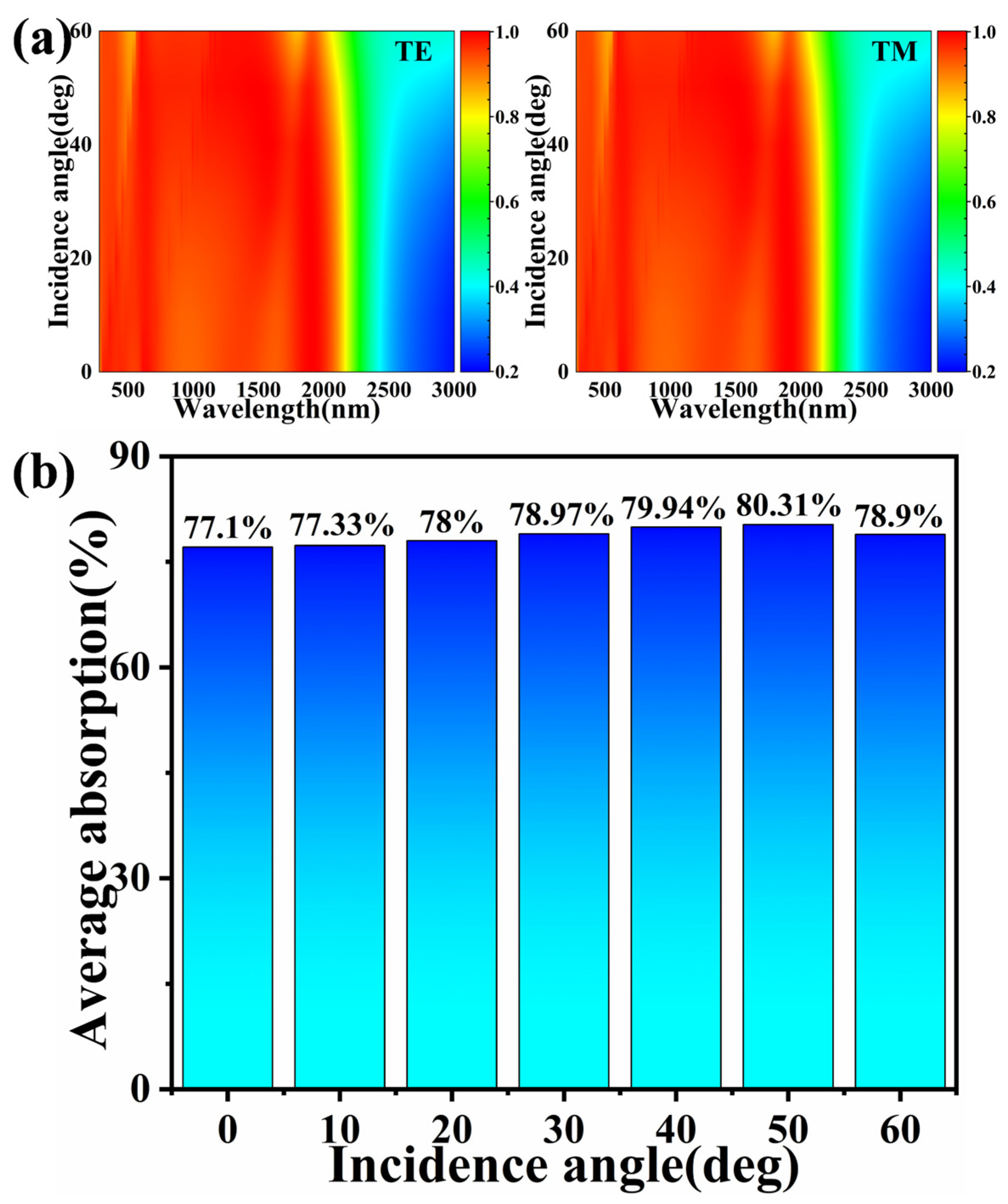
In order to realize the wide application of the SETR in natural environment, the design of the structure needs to satisfy the requirements of polarization independence and wide-incidence angle stability [75,76]. Because we adopt a fully symmetric design when designing the structure of the SETR, which indicates that the SETR has a polarization-independent property, the absorption efficiency is the same in both polarization modes (TE mode and TM mode) [77,78].
For this reason, we show the spectral scanning diagrams of the SETR in the TM and TE modes from 0° to 60°, as shown in Figure 11a. This shows that, no matter what the incidence angle is, the main loss of absorption occurs in the infrared band region after 2200 nm. With an increase in the incidence angle, the absorption loss of the SETR at 2500 nm is made up for, but there is a partial loss of absorption within the 2000 nm wavelength. This is also shown in the bar graph of the average absorption efficiency from 0° to 60° in Figure 11b. The average absorption at a 60° incidence angle is 78.9%, which is a decrease compared to the average absorption of 80.31% for an incidence angle of 50°. Between 0° and 50°, the SETR has been rising steadily. Therefore, future SETRs should be dedicated to solving the problem of decreasing absorption efficiency due to the change in the angle of the sun’s rays in real-world applications. It should also consider the effects of polarization in the complex atmosphere to provide the best solutions for the next generation of solar collectors and photovoltaic devices [79].

4. Conclusions

In this paper, we have designed an SETR structure based on the separation of the dielectric layer Al2O3 with metal W as a splitter column. It is important to note that we have filled the gap separated by the splitter column with a cross-shaped rectangular structure composed of GaAs-W. This novel design has enabled the SETR to achieve a bandwidth range of over 90% of the bandwidth, and the weighted average absorption was 95.22% in the 280–2500 nm band under AM1.5 conditions. Meanwhile, the thermal emission efficiencies at high temperatures of 1000 K, 1100 K, 1200 K, 1300 K, 1400 K, and 1500 K are 95.7%, 95.55%, 95.4%, 95.26%, 95.13%, and 95.01%, respectively, which are extremely good. We also looked at the results of the computer simulations for different types of cross-shaped rectangular structures made of GaAs-W, different split-column structures made of Al2O3-W, different SETR materials, and different parameter sizes. We found that our designed SETR performs best in terms of its structure, material, and size. We have finally looked at how the SETR absorbs light at different angles of sunlight. Because our SETR is perfectly symmetrical, we can confirm that the amount of light absorbed is the same for both polarized and unpolarized light, and does not change much if the angle of sunlight changes a lot. To sum up, the SETR that was designed works very well, is very efficient and can be used in a variety of complex environments. It is used a lot in real-life situations like thermo-electrics and thermal emission.

Author Contributions

Conceptualization, J.L. and J.G.; data curation, J.L., J.G. and P.W.; formal analysis, J.L., J.G., P.C. and Z.Y.; methodology, J.L., J.G., P.C. and Z.Y.; resources, G.Z., Y.S., P.C. and Z.Y.; software, G.Z. and Y.S.; data curation, G.Z., Y.S., P.C. and Z.Y.; writing—original draft preparation, P.W., P.C. and Z.Y.; writing—review and editing, J.L. and J.G. All authors have read and agreed to the published version of the manuscript.

Funding

The authors are grateful to the support provided by the National Natural Science Foundation of China (NOs. 51606158, 11604311, 12074151).

Institutional Review Board Statement

Not applicable.

Informed Consent Statement

Not applicable.

Data Availability Statement

Publicly available datasets were analyzed in this study. These data can be found here: [https://www.lumerical.com/] (accessed on 1 January 2020).

Conflicts of Interest

Authors Jiangtao Guo, Guangxu Zhao, Yan Shao were employed by the company China Coal Technology & Engineering Group Chongqing Research Institute Co., Ltd. The remaining authors declare that the research was conducted in the absence of any commercial or financial relationships that could be construed as a potential conflict of interest.

References

  1. Herrington, R. Mining our green future. Nat. Rev. Mater. 2021, 6, 456–458. [Google Scholar] [CrossRef] [Scilit]
  2. Zhao, Y.; Li, M.J.; Xu, Z.H.; Gao, C.G.; Liu, M.X. Preparation of Feather-like Bi2S3/Bi2O3 heterojunctions and Performance Study of Photocatalytic Reduction of Cr (Ⅵ). J. Southwest Univ. Sci. Technol. 2024, 39, 32–39+48. [Google Scholar] [CrossRef]
  3. Shi, W.Y.; Sun, X.F.; Xu, M.H.; Wang, S.F.; Liu, G.R.; Yang, H. Design of new CoFe2O4/MXene/NaTaO3 double heterostructures for efficient photodegradation of antibiotic. J. Water Process Eng. 2024, 67, 106229. [Google Scholar] [CrossRef] [Scilit]
  4. Liu, Y.J.; Liu, M.S.; Yang, H.; Yi, Z.; Zhang, H.; Tang, C.J.; Deng, J.; Wang, J.Q.; Li, B.X. Photoelectric simulation of perovskite solar cells based on two inverted pyramid structures. Phys. Lett. A 2025, 552, 130653. [Google Scholar] [CrossRef] [Scilit]
  5. Hu, H.; Chen, F.; Li, Y.; Li, J.; Cui, L.; Jiang, D.; Lin, X.; Gao, J. Construction of graphene supported TiO2 nanosheet array/CdS/Ni2P composite with dual heterojunctions for boosting photocatalytic hydrogen evolution. J. Alloys Compd. 2025, 1024, 180216. [Google Scholar] [CrossRef] [Scilit]
  6. Wang, P.; Yang, M.; Tang, S.; Li, Y.; Lin, X.; Zhang, H.; Zhu, Z.; Chen, F. Z-scheme heterojunctions composed of 3D graphene aerogel/g-C3N4 nanosheets/porous ZnO nanospheres for the efficient photocatalytic reduction of CO2 with H2O under visible light irradiation. J. Alloys Compd. 2022, 918, 165607. [Google Scholar] [CrossRef] [Scilit]
  7. Chen, S.; Wu, X.H.; Fu, C.J. Active tuning of anisotropic phonon polaritons in natural van der Waals crystals with negative permittivity substrates and its application in energy transport. Opto-Electron. Sci. 2024, 3, 240002. [Google Scholar] [CrossRef] [Scilit]
  8. Armas, D.; Matias, I.R.; Lopez-Gonzalez, M.C.; Zamarreño, C.R.; Zubiate, P.; Del Villar, I.; Romero, B. Generation of lossy mode resonances (LMR) using perovskite nanofilms. Opto-Electron. Adv. 2024, 7, 230072. [Google Scholar] [CrossRef] [Scilit]
  9. Zhou, A.X.; Liu, M.S.; Yi, Z.; Tang, C.J.; Deng, J.; Li, B.X. Design and Optimization of High-Efficiency Double-Layer CuO Perovskite Solar Cells. Phys. Status Solidi (RRL) Rapid Res. Lett. 2026, 20, e202500324. [Google Scholar] [CrossRef] [Scilit]
  10. Liu, X.Y.; Wang, Q.H.; Zhang, J.Y.; Hu, J.Y. An ultra-broadband solar absorber based on the biomimetic moth-eye-shaped Titanium nitride nanostructures. Phys. B Condens. Matter 2025, 716, 417757. [Google Scholar] [CrossRef] [Scilit]
  11. Wang, Q.H.; Ju, X.W.; Lin, Q.; Hu, J.Y. An ultra-broadband near-perfect solar absorber based on monolayer MoS2 with titanium ring-pillar arrays. Opt. Commun. 2025, 577, 131448. [Google Scholar] [CrossRef] [Scilit]
  12. Jalal, A.; Dong, Y.; Deng, B.W.; Qasim, M.; Moghaddasi, M.; Qureshi, U.U.R.; Wang, Z.Y.; Wu, X.D.; Xiong, C.J.; Hu, B. Bending-switchable terahertz metamaterial with a single layer based on laser-induced graphene. Chin. Opt. Lett. 2025, 23, 043603. Available online: https://opg.optica.org/col/abstract.cfm?uri=col-23-4-043603 (accessed on 3 February 2026). [CrossRef] [Scilit]
  13. Jo, Y.; Park, H.; Yoon, H.; Kim, I. Advanced biological imaging techniques based on metasurfaces. Opto-Electron. Adv. 2024, 7, 240122. [Google Scholar] [CrossRef] [Scilit]
  14. Ling, Z.X.; Zeng, Y.; Liu, G.D.; Wang, L.L.; Lin, Q. Unified model for plasmon-induced transparency with direct and indirect coupling in borophene-integrated metamaterials. Opt. Express 2022, 30, 21966. [Google Scholar] [CrossRef] [Scilit]
  15. Yang, H.; Xu, J.; Peng, M.Y.; He, H.R.; Jiang, Y.T.; Yu, D.; Jin, R.B.; Gu, Y.J.; Hu, Y.Q.; Duan, H.G.; et al. Vector analog computing via on-demand metasurface dispersive polarization transformation. Sci. Adv. 2025, 11, eadz5123. [Google Scholar] [CrossRef] [Scilit]
  16. Berhe, A.M.; As’ham, K.; Al-Ani, I.; Hattori, H.T.; Miroshnichenko, A.E. Strong coupling and catenary field enhancement in the hybrid plasmonic metamaterial cavity and TMDC monolayers. Opto-Electron. Adv. 2024, 7, 230181. [Google Scholar] [CrossRef] [Scilit]
  17. Landy, N.I.; Sajuyigbe, S.; Mock, J.J.; Smith, D.R.; Padilla, W.J. Perfect metamaterial absorber. Phys. Rev. Lett. 2008, 100, 207402. [Google Scholar] [CrossRef] [Scilit]
  18. Yang, H.; Ou, K.; Liu, Q.; Peng, M.Y.; Xie, Z.W.; Jiang, Y.T.; Jia, H.H.; Cheng, X.B.; Jing, H.; Hu, Y.Q.; et al. Metasurface higher-order poincaré sphere polarization detection clock. Light. Sci. Appl. 2025, 14, 63. [Google Scholar] [CrossRef] [Scilit]
  19. Lang, Q.Y.; Zou, C.G.; Zhang, Z.Y.; Wang, J.Q.; Liu, K.; Jiang, J.F.; Liu, T.G.; Cheng, Z.Z. Mid-infrared suspended silicon nanomembrane microring resonators with grating couplers. Chin. Opt. Lett. 2025, 23, 101302. [Google Scholar] [CrossRef] [Scilit]
  20. Xu, M.J.; Yan, D.X.; Wang, Y.; Li, X.J.; Zhang, L.; Li, J.N. Graphene-assisted dual-frequency third harmonic generation in nonlinear metamaterials for high-efficiency on-chip terahertz integration. Front. Phys. 2026, 21, 044201. [Google Scholar]
  21. Wu, P.H.; Zhao, W.C.; Cui, L.N.; Jiang, P.P. High absorption broadband solar energy device and thermal emitter based on titanium metamaterials. Int. J. Therm. Sci. 2026, 223, 110620. [Google Scholar] [CrossRef] [Scilit]
  22. Liu, H.; Li, J.; Yang, H.; Wang, J.; Li, B.; Zhang, H.; Yi, Y. TiN-Only Metasurface Absorber for Solar Energy Harvesting. Photonics 2025, 12, 443. [Google Scholar] [CrossRef] [Scilit]
  23. Yuan, Y.; Liu, H.F.; Liu, M.S.; Zhang, W.B.; Li, X.H.; Cheng, S.B. Design of wide-angle broadband titanium-nitride solar absorber based on column-cavity structure. Phys. Lett. A 2025, 556, 130832. [Google Scholar] [CrossRef] [Scilit]
  24. Zhou, Z.; Chen, Y.; Tian, Y.; Liang, J.; Yang, W. Ultra-broadband Metamaterial Perfect Solar Absorber with Polariza-tion-Independent and Large Incident Angle-Insensitive. Opt. Laser Technol. 2022, 156, 108591. [Google Scholar] [CrossRef] [Scilit]
  25. Liang, J.; Chen, Y.; Zhou, Z.; Chen, S. Multiband-switchability and High-Absorptivity of a Metamaterial Perfect Absorber Based on a Plasmonic Resonant Structure in the Near-Infrared Region. RSC Adv. 2022, 12, 30871–30878. [Google Scholar] [CrossRef] [Scilit]
  26. Gao, Z.; Yu, S.; Li, Z.; Pan, D.; Xu, Z.; Zhao, T. Ultra-Broadband Spectrally Selective Absorber for Solar Thermal Absorption Based on TiN Square-Ring Meta-Structure. IEEE Photonics J. 2023, 15, 4600207. [Google Scholar] [CrossRef] [Scilit]
  27. Ai, Z.; Yi, Y.T.; Yang, H.; Liu, M.S.; Yi, Y.G.; Tang, C.J.; Gao, F. TiN-Ti ultra-broadband solar absorber: Efficient heat absorption and high thermal stability. Phys. Lett. A 2025, 556, 130827. [Google Scholar] [CrossRef] [Scilit]
  28. Yang, Q.B.; Zeng, L.L.; Wang, M.H.; Guo, B.W.; Deng, Y.F.; Xu, S.X.; Li, B.X. Broadband Perfect Absorber Based on Graphene-silicon Mie Heterojunctions for cancer cell detection. Phys. E Low-Dimens. Syst. Nanostruct. 2025, 177, 116456. [Google Scholar] [CrossRef] [Scilit]
  29. Xu, L.L.; Yan, D.X.; Li, X.J.; Zhang, L.; Li, J.N. A metasurface structure-assisted terahertz negative curvature fiber. Phys. Scr. 2024, 99, 045525. [Google Scholar] [CrossRef] [Scilit]
  30. Jin, Z.Y.; Liu, M.S.; Cheng, S.B.; Yi, Z.; Wang, J.Q.; Li, B.X. Broadband tunable metasurface absorbing device in the terahertz band based on single-layer graphene. Mod. Phys. Lett. B 2026, 40, 2650017. [Google Scholar] [CrossRef] [Scilit]
  31. Yue, S.; Hou, M.; Wang, R.; Guo, H.; Hou, Y.; Li, M.; Zhang, Z.; Wang, Y.; Zhang, Z. Ultra-broadband Metamaterial Absorber from Ultraviolet to Long-Wave Infrared Based on CMOS-compatible Materials. Opt. Express 2020, 28, 31844–31861. [Google Scholar] [CrossRef] [Scilit] [PubMed]
  32. Zhou, Y.; Qin, Z.; Liang, Z.; Meng, D.; Xu, H.; Smith, D.R.; Liu, Y. Ultra-broadband Metamaterial Absorbers from Long to Very Long Infrared Regime. Light. Sci. Appl. 2021, 10, 138. [Google Scholar] [CrossRef] [Scilit]
  33. Wang, Q.H.; Ju, X.W.; Yang, C.; Zhang, Y.; Hu, J.Y. An ultra-narrow multi-band perfect absorber based on single dielectric nano-cylinder array with surface lattice resonance. Phys. Scr. 2025, 100, 035538. [Google Scholar] [CrossRef] [Scilit]
  34. Huang, X.; Lin, Q.; Xia, S.X.; Zhai, X.; Liu, G.D. Dynamic polarization control of strongly coupled quasi-guided modes enables high-efficiency THG. Opt. Express 2025, 33, 48707–48716. [Google Scholar] [CrossRef] [Scilit]
  35. Ma, Z.C.; Li, B.X.; Zeng, L.L.; Fan, Y.; Deng, Y.W.; Zhong, G.X.; Shao, Z.Z.; Xu, H.Q. Inverse Design of Plasmon-Induced Transparency in Stripe-Circular Aggregate Stacking Arrays via Deep Learning with Fewer Feature Points. Phys. E Low-Dimens. Syst. Nanostruct. 2025, 173, 116334. [Google Scholar] [CrossRef] [Scilit]
  36. An, K.; Liu, M.S.; Yang, H.; Yi, Z.; Tang, C.J.; Deng, J.; Wang, J.Q.; Li, B.X. Efficient broadband solar absorber and thermal emitter based on Ti and InAs with pyramid-like structure. Phys. E Low-Dimens. Syst. Nanostruct. 2026, 175, 116377. [Google Scholar] [CrossRef] [Scilit]
  37. Tian, M.; Wei, J.S.; Lv, E.G.; Li, C.H.; Liu, G.F.; Sun, Y.; Yang, W.; Wang, Q.Z.; Shen, C.C.; Zhang, C.; et al. Drug evaluation platform based on non-destructive and real-time in situ organoid fate state monitoring by graphene field-effect transistor. Chem. Eng. J. 2024, 498, 155355. [Google Scholar] [CrossRef] [Scilit]
  38. Zhao, C.C.; Yan, D.X.; Li, X.J.; Wang, Y.; Zhang, L.; Li, J.N. A single dual-frequency reflective metasurface for simultaneous multi-mode orbital angular momentum multiplexing. Opt. Commun. 2025, 575, 131313. [Google Scholar] [CrossRef] [Scilit]
  39. Palik, E.D. Handbook of Optical Constants of Solids; Academic Press: Boston, MA, USA, 1998. [Google Scholar]
  40. Ma, J.; Wang, B.; Xiong, Y. Recovery of metallic palladium from Explosives Production Waste liquid by electrochemical reduction with boron-doped diamond thin film electrode. J. Southwest. Univ. Sci. Technol. 2025, 40, 36–44. [Google Scholar] [CrossRef]
  41. Alexey, D.K. Optical spectra of plasmon–exciton core–shell nanoparticles: An anisotropic classical model eliminates discrepancies in experiments. Chin. Opt. Lett. 2024, 22, 093602. [Google Scholar]
  42. Sharbirin, A.S.; Kong, R.E.; Mato, W.B.; Tran, T.T.; Lee, E.; Khor, J.W.; Fadli, A.L.; Kim, J. Highly enhanced UV absorption and light emission of monolayer WS2 through hybridization with Ti2N MXene quantum dots and g-C3N4 quantum dots. Opto-Electron. Adv. 2024, 7, 240029. [Google Scholar] [CrossRef] [Scilit]
  43. Du, J.H.; Sun, X.F.; Wang, S.F.; Yi, Z.; Liu, G.R.; Yang, H. Boosting photocatalytic synthesis of H2O2 via p-type Schottky junction-mediating free electron and photoelectron transfer behavior. Appl. Surf. Sci. 2026, 719, 165024. [Google Scholar] [CrossRef] [Scilit]
  44. Xu, S.C.; Tian, M.; Li, C.H.; Liu, G.F.; Wang, J.H.; Yan, T.T.; Li, Z. Using a crumpled graphene field-effect transistor for ultrasensitive SARS-CoV-2 detection via its papain-like protease. Chem. Eng. J. 2025, 505, 159386. [Google Scholar] [CrossRef] [Scilit]
  45. Nie, Q.P.; Zhang, D.Y. Hot spot light radiation characteristics of energetic powder DAAF under strong impact. J. Southwest. Univ. Sci. Technol. 2024, 39, 30–35+56. [Google Scholar] [CrossRef]
  46. Li, L.; Yi, Z.; Cheng, S.B.; Tang, C.J.; Gao, F.; Li, B.X. Simulation Research on Broadband and High-Efficiency Solar Absorber Based on Spiral Metasurface. Phys. Status Solidi (RRL) Rapid Res. Lett. 2026, e202500447. [Google Scholar] [CrossRef] [Scilit]
  47. Liu, G.F.; Wang, Z.X.; Sun, W.; Lin, X.H.; Wang, R.; Li, C.H.; Zong, L.; Fu, Z.L.; Liu, H.P.; Xu, S.C. Robust emission in near-infrared II of lanthanide nanoprobes conjugated with Au (LNPs-Au) for temperature sensing and controlled photothermal therapy. Chem. Eng. J. 2023, 452, 139504. [Google Scholar] [CrossRef] [Scilit]
  48. Luo, M.H.; Hu, J.Y.; Li, Y.M.; Bai, W.D.; Zhang, R.L.; Lin, Q.; Wang, L.L. Anapole-assisted ultra-narrow-band lattice resonance in slotted silicon nanodisk arrays. J. Phys. D Appl. Phys. 2023, 56, 375102. [Google Scholar] [CrossRef] [Scilit]
  49. Zhao, H.M.; Wang, X.Y.; Lin, Q.; Zhai, X.; Liu, G.D. High-efficiency control of cross-polarization conversion at communication wavelengths using a tunable borophene-plasmonic metasurface. J. Phys. D Appl. Phys. 2026, 59, 025105. [Google Scholar] [CrossRef] [Scilit]
  50. Li, Y.R.; Liu, W.H.; Liu, R.C.; Gao, J.J.; Feng, J.W.; Xu, S.C.; Li, Z.; Jiang, S.Z.; Du, X.J. 3D hybrid arrayed Ag/MOF multi-plasmon resonant cavity system for high-performance SPR sensing. Opt. Laser Technol. 2023, 167, 109825. [Google Scholar] [CrossRef] [Scilit]
  51. Liu, L.; Liu, W.; Liu, Q.; Chen, Y.; Yang, X.; Zhang, Y.; Yi, Z. Synergistic Energy Level Alignment and Light-Trapping Engineering for Optimized Perovskite Solar Cells. Coatings 2025, 15, 856. [Google Scholar] [CrossRef] [Scilit]
  52. Wu, D.; Liu, C.; Liu, Y.; Xu, Z.; Yu, Z.; Yu, L.; Chen, L.; Ma, R.; Zhang, J.; Ye, H. Numerical Study of a Wide-Angle Polarization-Independent Ultra-Broadband Efficient Selective Metamaterial Absorber for Near-Ideal Solar Thermal Energy Conversion. RSC Adv. 2018, 8, 21054–21064. [Google Scholar] [CrossRef] [Scilit] [PubMed]
  53. Ye, Q.; Chen, M.; Cai, W. Numerically Investigating a Wide-Angle Polarization-Independent Ultra-Broadband Solar Selective Absorber for High-Efficiency Solar Thermal Energy Conversion. Sol. Energy 2019, 184, 489–496. [Google Scholar] [CrossRef] [Scilit]
  54. Shuvo, M.M.K.; Hossain, M.I.; Rahman, S.; Mahmud, S.; Islam, S.S.; Islam, M.T. A Wide-Angle, Enhanced Oblique Incidence, Bend-Able Metamaterial Absorber Employed in Visible Region with a Sun Shape Resonator. IEEE Access 2021, 9, 126466–126480. [Google Scholar] [CrossRef] [Scilit]
  55. Jiang, X.; Zhou, L.; Hu, J.; Wang, T. Nanostructured Multilayer Hyperbolic Metamaterials for High Efficiency and Selective Solar Absorption. Opt. Express 2022, 30, 11504–11513. [Google Scholar] [CrossRef] [Scilit]
  56. Chen, X.M.; Yan, D.X.; Wang, Y.; Zhang, L.; Sun, S.; Li, J.N. Two Novel Mechanisms for Suppressing Higher-Order Radial Modes in Dual-Ring Core Hollow-Core Fibers for OAM Transmission. J. Light. Technol. 2025, 43, 9382–9395. [Google Scholar] [CrossRef] [Scilit]
  57. Chen, Z.Y.; Liu, M.S.; Cheng, S.B.; Wang, J.Q.; Yi, Y.G.; Li, B.X.; Tang, C.J.; Gao, F. Bilayer Graphene Metasurface with Dynamically Reconfigurable Terahertz Perfect Absorption. Curr. Appl. Phys. 2025, 80, 282–290. [Google Scholar] [CrossRef] [Scilit]
  58. Zeng, Y.X.; Li, B.X.; Zeng, L.L.; Zhong, G.X.; Shao, Z.Z.; Xu, H.Q.; Liu, M.L.; Chen, Z.G.; Dai, C.J. High sensitivity and ultra-narrowband perfect metamaterial absorber based on graphene metasurface. Eur. Phys. J. Plus 2025, 140, 416. [Google Scholar] [CrossRef] [Scilit]
  59. Yi, Y.X.; Yi, Z.; Zhou, Z.G.; Yang, H.; Wang, J.Q.; Tang, C.J.; Deng, J.; Li, B.X. Structural design and analysis of D-type elliptical open-loop photonic crystal fiber temperature sensor based on SPR. Phys. B Condens. Matter 2025, 715, 417549. [Google Scholar] [CrossRef] [Scilit]
  60. Wang, H.Y.; Ma, R.; Liu, G.D.; Wang, L.L.; Lin, Q. Optical force conversion and conveyor belt effect with coupled graphene plasmon waveguide modes. Opt. Express 2023, 31, 32422. [Google Scholar] [CrossRef] [Scilit] [PubMed]
  61. Yang, J.Q.; Lin, Q.; Wang, L.L.; Liu, G.D. Research of bound states in the continuum and their polarization control in dielectric metamaterials. Phys. Scr. 2025, 100, 065551. [Google Scholar] [CrossRef] [Scilit]
  62. Zhu, Z.H.; Yan, D.X.; Xu, L.L.; Li, X.J.; Zhang, L.; Li, J.N. Terahertz Ring-Core Fiber for First-Order Radial OAM Modes Transmission Without Phase Distortion. IEEE J. Sel. Top. Quantum Electron. 2024, 30, 4300610. [Google Scholar] [CrossRef] [Scilit]
  63. Wang, J.; Liu, M.S.; Yang, H.; Yi, Z.; Tang, C.J.; Gao, F.; Wang, J.Q.; Li, B.X. Tunable mid-infrared ultra-wideband absorption device with annular-square open metamaterials based on VO2 phase change. Micro Nanostruct. 2025, 208, 208353. [Google Scholar] [CrossRef] [Scilit]
  64. Fan, Y.; Li, B.X.; Zeng, L.L.; Ma, Z.C.; Deng, Y.W.; Shao, Z.Z. Dual-quasi BIC enabled plasmonic metasurfaces and active switch between BIC and quasi-BIC. Phys. Scr. 2025, 100, 055905. [Google Scholar] [CrossRef] [Scilit]
  65. Yang, C.; Luo, M.H.; Ju, X.W.; Hu, J.Y. Ultra-narrow dual-band perfect absorber based on double-slotted silicon nanodisk arrays. J. Phys. D Appl. Phys. 2024, 57, 345104. [Google Scholar] [CrossRef] [Scilit]
  66. Ai, Z.; Yang, H.; Liu, M.S.; Cheng, S.B.; Wang, J.Q.; Tang, C.J.; Gao, F.; Li, B.X. Phase-Transition-Enabled Dual-Band Camouflage in VO2/Ag Multilayered Nanostructures. Phys. E Low-Dimens. Syst. Nanostruct. 2025, 173, 116327. [Google Scholar] [CrossRef] [Scilit]
  67. Liu, Z.Y.; Huang, Y. Preparation and Properties of Self-healing P(BA-co-NIAM)/ILs-rGO Composites. J. Southwest Univ. Sci. Technol. 2024, 39, 1–9. [Google Scholar] [CrossRef]
  68. Li, Z.T.; Li, X.; Liu, G.D.; Wang, L.L.; Lin, Q. Analytical investigation of unidirectional reflectionless phenomenon near the exceptional points in graphene plasmonic system. Opt. Express 2023, 31, 30458. [Google Scholar] [CrossRef] [Scilit]
  69. Yang, Q.L.; Zeng, L.L.; Li, B.X. Independently tunable dual-channel angle-sensitive narrow-band perfect absorber. Appl. Opt. 2025, 64, 1464–1470. [Google Scholar] [CrossRef] [Scilit]
  70. Hu, J.Y.; Tan, C.X.; Bai, W.D.; Li, Y.M.; Lin, Q.; Wang, L.L. Dielectric nanocavity-coupled surface lattice resonances for high-efficiency plasmonic sensing. J. Phys. D Appl. Phys. 2022, 55, 075105. [Google Scholar] [CrossRef] [Scilit]
  71. Wang, J.; Liu, M.S.; Yang, H.; Yi, Z.; Tang, C.J.; Deng, J.; Wang, J.Q.; Li, B.X. Far-infrared broadband metamaterial absorption device based on the Ti-TiO2 -GaAs-Ti structure. Opt. Commun. 2025, 596, 132415. [Google Scholar] [CrossRef] [Scilit]
  72. Yu, J.; Shi, J.F.; Qiu, R.; Guo, D.C.; Zhou, L. DKDP crystal Damage Detection Based on Gray-scale Adaptive Enhancement. J. Southwest. Univ. Sci. Technol. 2024, 39, 93–101. [Google Scholar] [CrossRef]
  73. Wang, L.; Lin, Q.; Wang, L.L.; Liu, G.D. Tunable high-Q perfect absorber by employing doubly degenerate quasi-bound states in the continuum. J. Appl. Phys. 2025, 137, 234303. [Google Scholar] [CrossRef] [Scilit]
  74. Ma, R.; Zhang, L.G.; Zeng, Y.; Liu, G.D.; Wang, L.L.; Lin, Q. Extreme enhancement of optical force via the acoustic graphene plasmon mode. Opt. Express 2023, 31, 482723. [Google Scholar] [CrossRef] [Scilit]
  75. Peng, C.; Yao, J.; Tsai, D.P. Progress in metalenses: From single to array. Opto-Electron. Technol. 2025, 1, 250004. [Google Scholar] [CrossRef] [Scilit]
  76. Liao, X.; Lin, Q.; Zhai, X.; Wang, L.L.; Liu, G.D. Bandwidth-Enhanced coherent perfect absorption based on tunable coupling of borophene nanoribbons. Phys. Scr. 2025, 100, 095514. [Google Scholar] [CrossRef] [Scilit]
  77. Zeng, L.L.; Li, B.X.; Wen, R.Q.; Zhang, X.J. Plasmonic Sensor Based on Multi Fano Resonance in Inverse T Shape Structure for Detection of CO2 Concentration. IEEE Photonics J. 2023, 15, 2201805. [Google Scholar] [CrossRef] [Scilit]
  78. Silva Oliveira, V.; Camboim, M.M.; Protasio de Souza, C.; Silva Guedes de Lima, B.A.; Baiocchi, O.; Kim, H.-S. A Thermoelectric Energy Harvester Based on Microstructured Quasicrystalline Solar Absorber. Micromachines 2021, 12, 393. [Google Scholar] [CrossRef] [Scilit]
  79. Faddouli, A.; Labrim, H.; Fadili, S.; Habchi, A.; Hartiti, B.; Benaissa, M.; Hajji, M.; EZ-Zahraouy, H.; Ntsoenzok, E.; Benyoussef, A. Numerical Analysis and Performance Investigation of New Hybrid System Integrating Concentrated Solar Flat Plate Collector with a Thermoelectric Generator System. Renew. Energy 2020, 147, 2077–2090. [Google Scholar] [CrossRef] [Scilit]
Figure 1. (a) Schematic of the three-dimensional structure of a single SETR; (b) shows the top view of the SETR.
Coatings 16 00211 g001
Figure 3. (ac) The schematic structure of the SETR in the XOY direction, the electric field distribution at λ = 626.5 nm, 1913 nm; (df) the schematic structure of the SETR in the XOZ direction, the electric field distribution at λ = 626.5 nm, 1913 nm.
Coatings 16 00211 g003
Figure 4. A comparison of the energy emission of the SETR for temperature changes from 1000 K to 1500 K.
Coatings 16 00211 g004
Figure 5. (a) The energy emission from the SETR in the 280–3000 nm band at different temperatures; (b) the energy emission from the SETR in the 280–2096 nm band at different temperatures.
Coatings 16 00211 g005
Figure 6. (a) is the absorption efficiencies of the SETR under three different configurations; (b) is the schematic structure of the SETR under three different configurations.
Coatings 16 00211 g006
Figure 7. (ac) Electric field diagrams in the XOY direction for the three cases at λ = 626.5 nm. (df) electric field diagrams in the XOZ direction for the three cases at λ = 626.5 nm.
Coatings 16 00211 g007
Figure 8. (a) Three-dimensional structure of case 4 with corresponding absorption efficiency; (b) three-dimensional structure of case 5 with corresponding absorption efficiency.
Coatings 16 00211 g008
Figure 9. (a) The absorption efficiency of the SETR with three different materials; (b) the side view of the SETR with three different materials.
Coatings 16 00211 g009
Figure 10. (a) Absorption efficiency plot for varying GaAs layer thickness H4; (b) absorption efficiency plot for varying Al2O3 layer thickness H6; (c) absorption efficiency plot for varying the width L of the symmetric gap of the split column; (d) absorption efficiency plot for varying the radius R of the split column.
Coatings 16 00211 g010
Figure 11. (a) The spectral scan of the SETR from 0° to 60° in TM and TE modes; (b) a bar graph of the average absorption efficiency from 0° to 60° in TM or TE modes.
Coatings 16 00211 g011
Table 1. Comparison with Other Literature.
Reference[52][53][54][55]Our Work
StructurePorous curved surface of W/SiO2 layerStacking of W sphere array and W gratingPatch absorber based on
W-SiO2
Nanostructured multilayer hyperbolic metamaterialsSymmetric gap separation of Al2O3 and W
Average absorptivity98.95%
(260–1580 nm)
>95%
(300–1777 nm)
96.43%
(390–770 nm)
>90%
(300–1726 nm)
94.994%
(280–2096 nm)
Thermal emission efficiency90.32%
(373.15 K)
92.23%
(373.15 K)
/95.5%
(600 K)
95.01%
(1000 K)
Absorption peak99%99%99.999%99%99.944%
Absorption of incident angle60°
(>90%)
/60°
(83.78%)
/50°
(80.31%)
Disclaimer/Publisher’s Note: The statements, opinions and data contained in all publications are solely those of the individual author(s) and contributor(s) and not of MDPI and/or the editor(s). MDPI and/or the editor(s) disclaim responsibility for any injury to people or property resulting from any ideas, methods, instructions or products referred to in the content.