


Abstract
Since their breakthrough development, dye-sensitized solar cells (DSSCs) have emerged as highly promising third-generation photovoltaics; however, interfacial charge carrier recombination remains a persistent bottleneck. This study investigates the application of a wide bandgap ZrO2 electron blocking layer (EBL) to mitigate this recombination. A 48 nm ZrO2 EBL was deposited on fluorine-doped tin oxide (FTO) via hydrothermal treatment. Empirical results demonstrate a remarkable 43.9% enhancement in overall power conversion efficiency (6.77%) and a 69% improvement in total Incident Photon-to-Current Efficiency (IPCE) compared to bare FTO architectures. To theoretically validate the role of an insulating material as an EBL, the empirical data is supported by mathematical modeling, specifically utilizing Wentzel–Kramers–Brillouin (WKB) quantum tunneling probabilities and 1D diffusion–recombination kinetics. The models confirm that at nanoscale thicknesses, ZrO2 acts as a selective physical barrier that shifts the surface Fermi level and extends the electron lifetime to 0.0146 s. Furthermore, potential optimization pathways utilizing machine learning algorithms for ideal thickness prediction and IPCE clustering are discussed, paving the way for next-generation predictive device engineering. Ultimately, this dual empirical–theoretical approach provides a comprehensive understanding of the interfacial charge transport mechanisms, establishing a robust framework for designing highly efficient, leak-free photoanode architectures in next-generation photovoltaics.
1. Introduction
Since their breakthrough development by Grätzel and O’Regan in 1991, dye-sensitized solar cells (DSSCs) have established themselves as one of the most promising third-generation photovoltaic technologies. Compared to conventional silicon-based p-n junction devices, DSSCs offer highly attractive features: they require low-energy and cost-effective manufacturing processes, utilize non-toxic materials, and provide excellent performance under low-light or indoor environments [1,2]. Furthermore, their semi-transparency and color tunability make them ideal candidates for building-integrated photovoltaics (BIPV) and next-generation flexible electronic systems [3]. The fundamental operation of a DSSC relies on a continuous kinetic cycle. Photosensitizing dye molecules absorb incident photons and enter an excited state. These excited electrons are subsequently injected into the conduction band of a mesoporous wide-bandgap semiconductor typically TiO2, ZnO, or SnO2 which is deposited onto a transparent conductive oxide (TCO) substrate, such as fluorine-doped tin oxide (FTO) [4,5]. The injected electrons percolate through the nanoparticle network to the external circuit, while the oxidized dye is continuously regenerated by a redox mediator in the electrolyte [6]. Despite recent advancements pushing the limits of DSSC performance, a persistent bottleneck in achieving higher power conversion efficiency (η) remains interfacial charge carrier recombination [7]. Because the mesoporous TiO2 layer is inherently highly porous, regions of the bare TCO substrate remain exposed directly to the electrolyte. This direct contact induces a “short-circuit” effect, allowing for the backward transfer (leakage) of photogenerated electrons from the FTO back into the redox electrolyte, thus severely limiting the cell’s open-circuit voltage (Voc) and overall conversion efficiency [8,9].
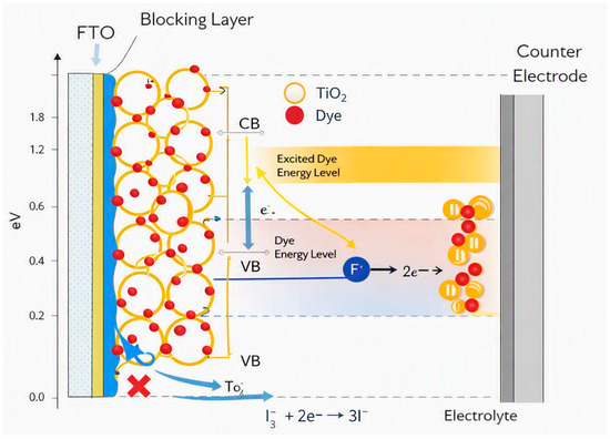
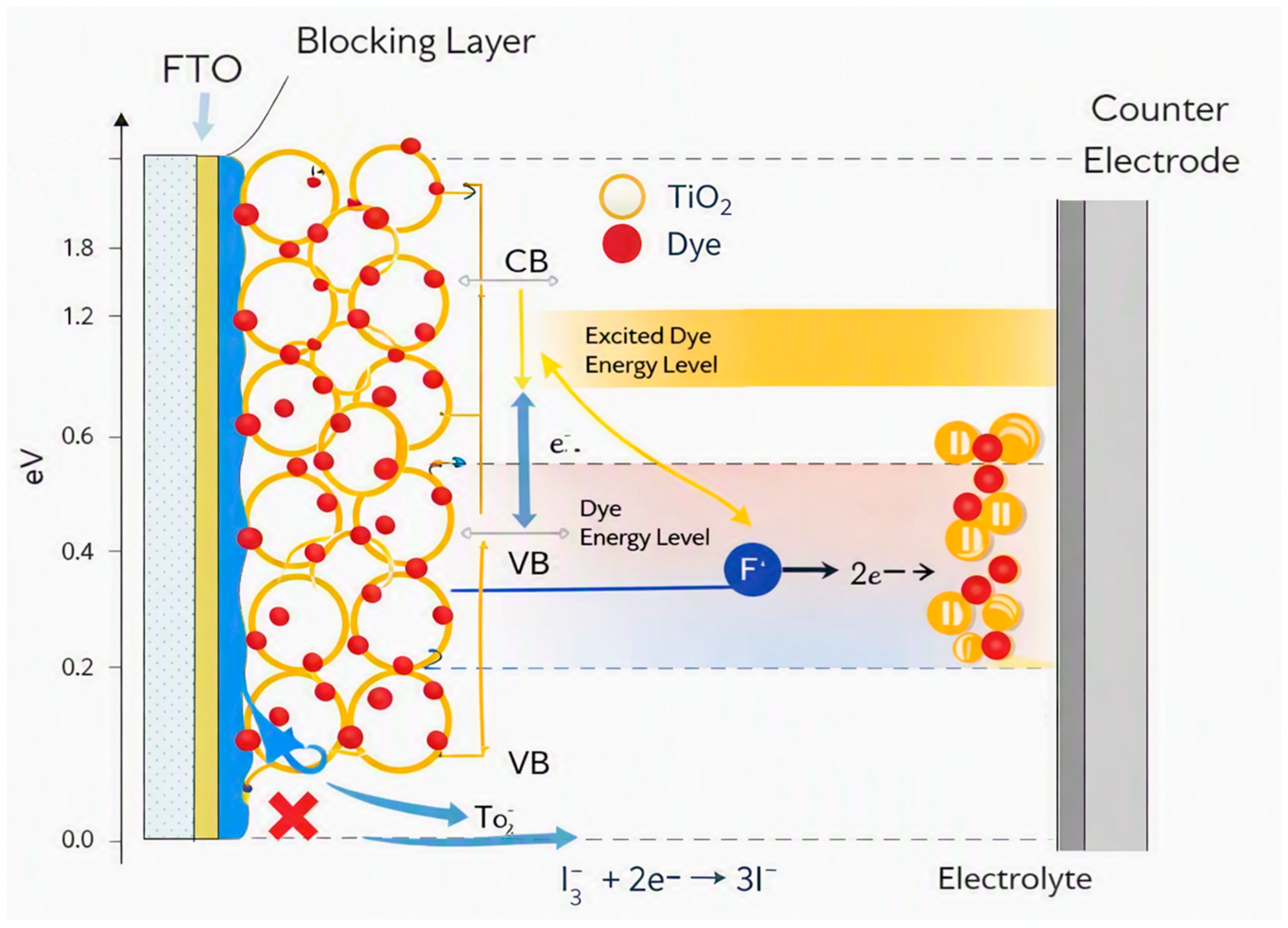
To suppress this undesirable reverse electron motion, the integration of an Electron Blocking Layer (EBL)—also known as a compact layer—between the FTO and the mesoporous semiconductor has become a critical device engineering strategy (Figure 1) [10]. An ideal EBL must fully cover the conductive substrate to isolate it from the electrolyte, while remaining thin enough to permit efficient forward electron conduction to the FTO [11]. Traditionally, a dense TiO2 thin film prepared via TiCl4 hydro-thermal treatment or spray pyrolysis is employed as the EBL [12,13]. However, depositing a dense TiO2 layer directly on the TCO often reduces optical transparency in the visible spectrum, thereby limiting the photon flux reaching the dye molecules. Consequently, recent research has pivoted toward wider band-gap metal oxides—such as Al2O3, ZnO, and SnO2—to formulate multi-functional heterojunction compact layers [14,15]. While ZrO2 has seen application as an insulating barrier in perovskite solar cells, to the best of our knowledge, its potential as a highly transparent EBL deposited directly onto FTO for liquid-state DSSCs has not been systematically reported. ZrO2 possesses a wide band gap, excellent thermal stability, and robust chemical inertness, making it a theoretically ideal candidate to block electron leakage without sacrificing the transparency of the photoanode. In this work, the EBL performance of ZrO2 in DSSCs is realized and thoroughly analyzed for the first time. We establish the optimal hydrothermal experimental conditions required to produce a highly transparent ZrO2 EBL that effectively minimizes electron leakage while maintaining a low charge carrier resistance. The optical and electronic characteristics at the interfacial region between the mesoporous TiO2 and the ZrO2 EBL are investigated using UV-Vis spectroscopy. Furthermore, Current Density–Voltage (J-V) characteristics, Electrochemical Impedance Spectroscopy (EIS), and Incident Photon-to-Current Efficiency (IPCE) analyses are conducted to provide a comprehensive understanding of the kinetics governing the enhanced photovoltaic properties of the ZrO2 modified cells. To rigorously substantiate the empirical observations and convince the broader materials science community of the viability of an insulating material as an EBL, this study transitions from bulk conductivity assumptions to interfacial thin-film physics. By integrating mathematical modeling strategies—specifically quantum tunneling probability calculations and recombination kinetics models solved via MATLAB R2026B—we establish a robust theoretical foundation for the charge transport mechanisms. Ultimately, this dual empirical-theoretical approach not only elucidates the exact physical barrier effects of the ZrO2 layer but also introduces modern machine learning concepts as viable tools for future EBL optimization.
Figure 1.
Schematic illustration of the blocking layer mechanism in a dye-sensitized solar cell (DSSC).
2. Materials and Methods
2.1. Production of Blocking Layers
The fabrication of the blocking layers was carried out via a hydrothermal methodology. Initially, commercial fluorine-doped tin oxide (FTO) substrates (TEC15, Pilkington, Ormskirk, UK) underwent a sequential ultrasonic cleaning process utilizing a detergent solution, deionized water, acetone, and isopropanol, with each step lasting 15 min. The substrates were subsequently dried under a steady stream of nitrogen gas. Prior to the fabrication of the TiO2 photoanode, electron blocking layers were deposited onto the conductive surface of the FTO glass. A TiO2 blocking layer was synthesized via a TiCl4 hydrothermal treatment [13]. Alternatively, the ZrO2 blocking layer was deposited by immersing the FTO substrates in a 5 mM solution of zirconium (IV) n-propoxide (Sigma-Aldrich, Darmstadt, Germany) dissolved in ethanol (Sigma-Aldrich Germany). This hydrothermal reaction was conducted in a Teflon-lined autoclave at 80 °C for 1.5 h, followed by an annealing process at 500 °C for 2 h.
2.2. DSSC Fabrication
The photoanodes were fabricated by depositing a TiO2 paste (Dyesol DSL-90T Australia) onto the bare FTO, TiO2/FTO, and ZrO2/FTO substrates using a screen-printing technique with a 90T mesh [16]. Surface profilometry measurements confirmed an active cell area of 0.25 cm2 and a mesoporous TiO2 film thickness of 14 µm. Following deposition, the photoanodes were dried at 120 °C for 30 min. A multi-step thermal annealing process was then performed under an ambient atmosphere at 325 °C for 5 min, 375 °C for 15 min, 450 °C for 15 min, and finally 500 °C for 15 min. Upon cooling, the annealed photoanodes were sensitized by immersion in a 0.5 mM N719 dye solution (Solaronix, Aubonne, Switzerland) at room temperature for 24 h in a dark environment. The counter electrodes were prepared utilizing a 5 mM ethanolic solution of hexa-chloro-platinic acid hexahydrate (H2PtCl6.6H2O). A droplet of this precursor solution was spin-coated onto the FTO substrate, followed by thermal treatment at 400 °C for 15 min to facilitate platinum deposition. To assemble the devices, the photoanode and the platinum counter electrode were sandwiched and sealed using a 25 μm thick Surlyn thermoplastic gasket (Dow-Türkiye, İstanbul, Turkey) at 100 °C. A liquid redox electrolyte (Solaronix AN50, Aubonne, Switzerland) was subsequently injected into the internal cavity via pre-drilled holes in the counter electrode. These injection ports were then hermetically sealed with additional Surlyn film, and the completed DSSCs were immediately subjected to photovoltaic characterization [17]. To ensure the statistical reliability and reproducibility of the results, five independent devices (N = 5) were fabricated and tested for each electrode configuration.
2.3. Mathematical Modeling Strategy
To predict charge transport and theoretically validate the suppression of interfacial recombination, a quantum tunneling model and recombination kinetics equations were formulated utilizing MATLAB scripts. Since bulk ZrO2 is fundamentally an insulator, electrons injected from the dye into the TiO2 network must reach the FTO without recombining with the I3− ions in the electrolyte. The probability of electron tunneling, T(E), through the dielectric ZrO2 layer is mathematically expressed as [18]:
where d is the barrier thickness 48 nm (in Figure 2e), h is Planck’s constant, m* is the effective mass of the electron, and () is the potential barrier height. Concurrently, to demonstrate how the ZrO2 layer minimizes electron leakage, the charge conservation and continuity equation for electrons in the mesoporous TiO2 network was modeled [19]
Figure 2.
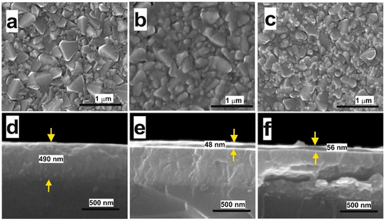
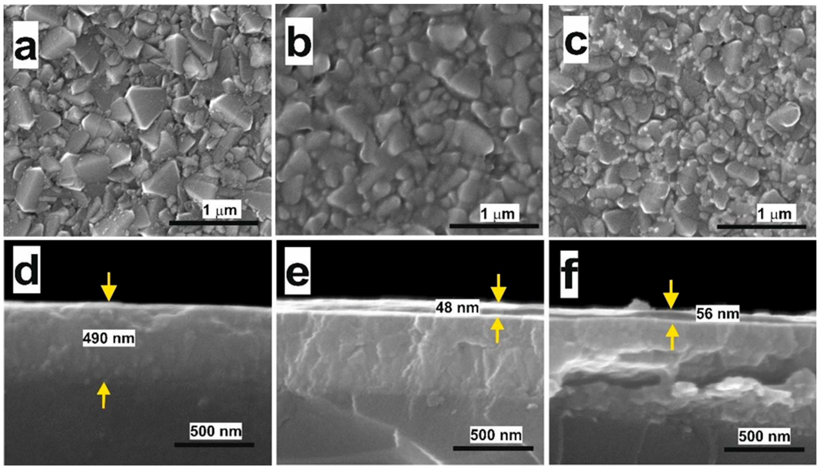
Top-view FE-SEM images of bare FTO (a), ZrO2/FTO (b), and TiO2/FTO (c); cross-sectional FE-SEM images of bare FTO (d), ZrO2/FTO (e), and TiO2/FTO (f). The thickness of the FTO layers was about 490 nm, and those of ZrO2 and TiO2 were about 48 and 56 nm, respectively.
Here, Dn represents the electron diffusion coefficient, krec is the recombination rate constant, and G denotes the generation rate. In Equation (2), represents the total dynamic electron concentration in the TiO2 conduction band under illumination, while denotes the thermal equilibrium electron density in the dark. The term () dictates the excess charge carriers driving the recombination kinetics. This differential model is utilized to fit the electrochemical impedance parameters, specifically the Z1 interface charge transport resistance and the Z2 interface resistance, to physically quantify the reduced leakage [20,21].
The physical parameters utilized in the 1D diffusion–recombination model were defined as follows: effective electron mass () for the ZrO2 layer = (where is the rest mass of an electron), potential barrier height () representing the conduction band offset at the interface = 1.5 eV, electron diffusion coefficient () = m2/s for TiO2 and m2/s for ZrO2 recombination rate constant () = 68.49 s−1 (derived from s), maximum generation rate () = m−3 s−1 with an exponential decay profile, and thermal equilibrium electron density () = m−3.
The one-dimensional continuity equation was solved numerically employing the explicit finite difference method (Forward Euler). The spatial domain was defined across the TiO2 network and the EBL interface using a uniform numerical grid (Nx = 400) with a spatial step size () of approximately 35.3 nm. To ensure numerical stability, the temporal evolution was simulated using a dynamically calculated time step ( s) until a steady-state condition was achieved at s. Regarding the initial and boundary conditions, a uniform equilibrium concentration () was set at . A Dirichlet boundary condition () was applied at the left contact interface (), while a zero-flux Neumann boundary condition () was established at the TiO2/electrolyte boundary.
3. Results
3.1. Morphological and Compositional Analyses of Coated and Uncoated FTO Surfaces
Field-emission scanning electron microscopy (FE-SEM) was utilized to evaluate the thickness and surface morphology of the respective films (Figure 2). The micrographs indicate a highly uniform deposition for the ZrO2 layer, whereas the TiO2 layer exhibited slight sedimentation phenomena intrinsic to the TiCl4 hydrothermal treatment. Cross-sectional analysis determined the bare FTO substrate thickness to be approximately 490 nm. The compact TiO2 and ZrO2 blocking layers exhibited thicknesses of 56 nm and 48 nm, respectively. Given the marginal dimensional variance between the two electron blocking layers (EBLs), their functional photovoltaic performances can be reliably compared [22].
X-ray photoelectron spectroscopy (XPS) is a highly sensitive surface analytical technique widely employed to investigate the dispersion, stoichiometric composition, and interfacial interactions of metal oxide films on conductive substrates [23,24]. Consequently, XPS was performed to confirm the structural integrity of the ZrO2 layer on the FTO.
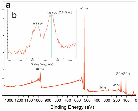
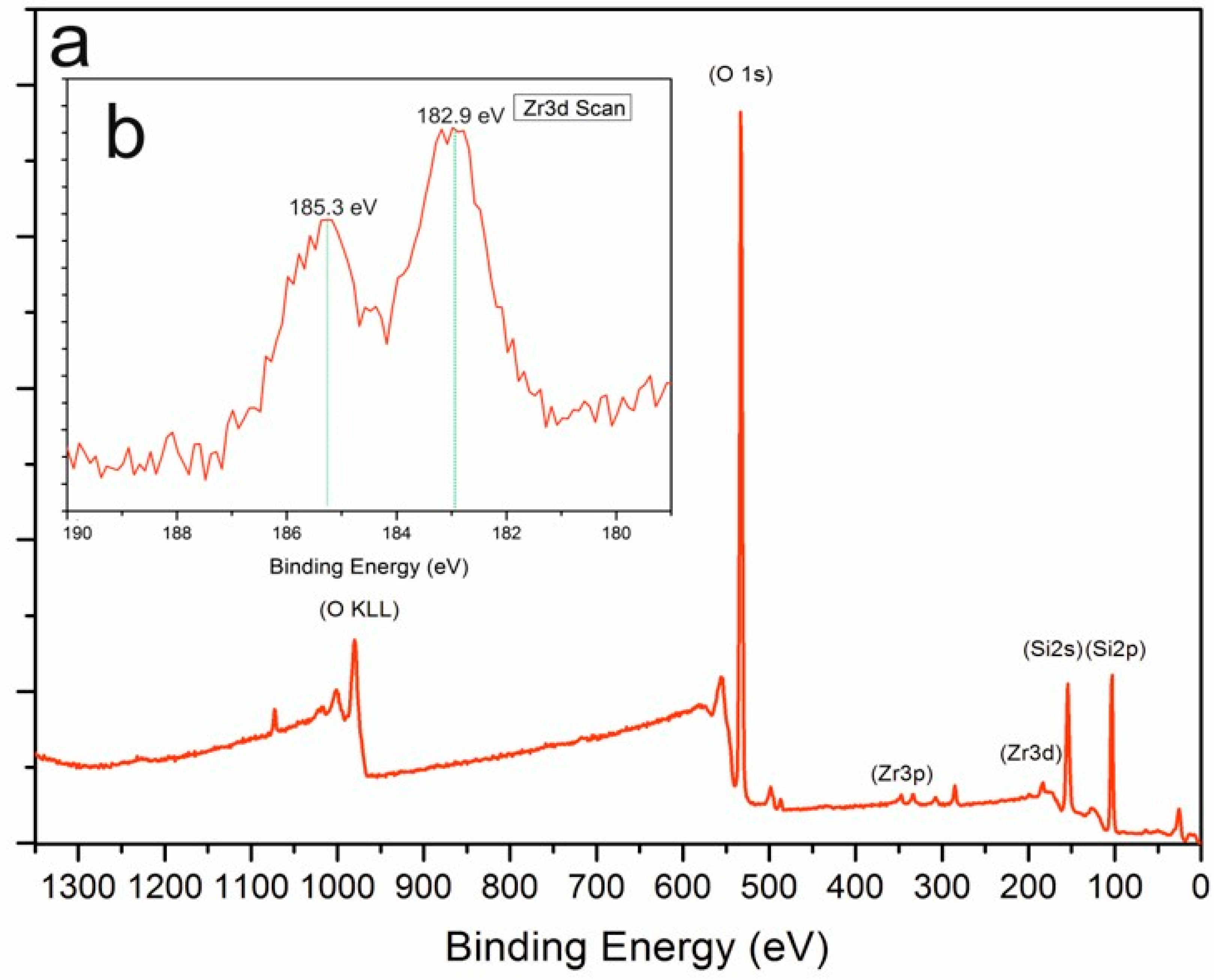
The survey spectrum of the ZrO2/FTO sample is depicted in Figure 3a. Furthermore, the high-resolution Zr 3d spectrum (Figure 3b) extracted from the 48 nm film reveals a characteristic 3d doublet splitting of 2.4 eV. The prominent Zr 3d5/2 peak is positioned at a binding energy of 182.9 eV, which is in excellent agreement with standard values for ZrO2 [25], thereby confirming the successful deposition of a pure ZrO2 blocking layer.
Figure 3.
XPS survey spectrum with surface composition of ZrO2/FTO sample (a) and Zr 3d XPS spectra of ZrO2/FTO sample (b).
3.2. Optical Properties and UV-Vis Spectroscopy
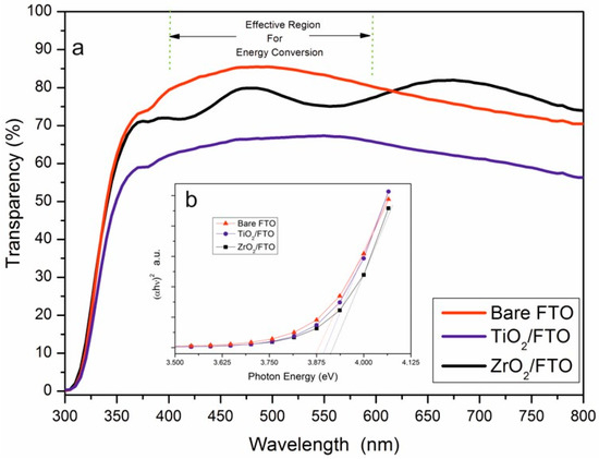
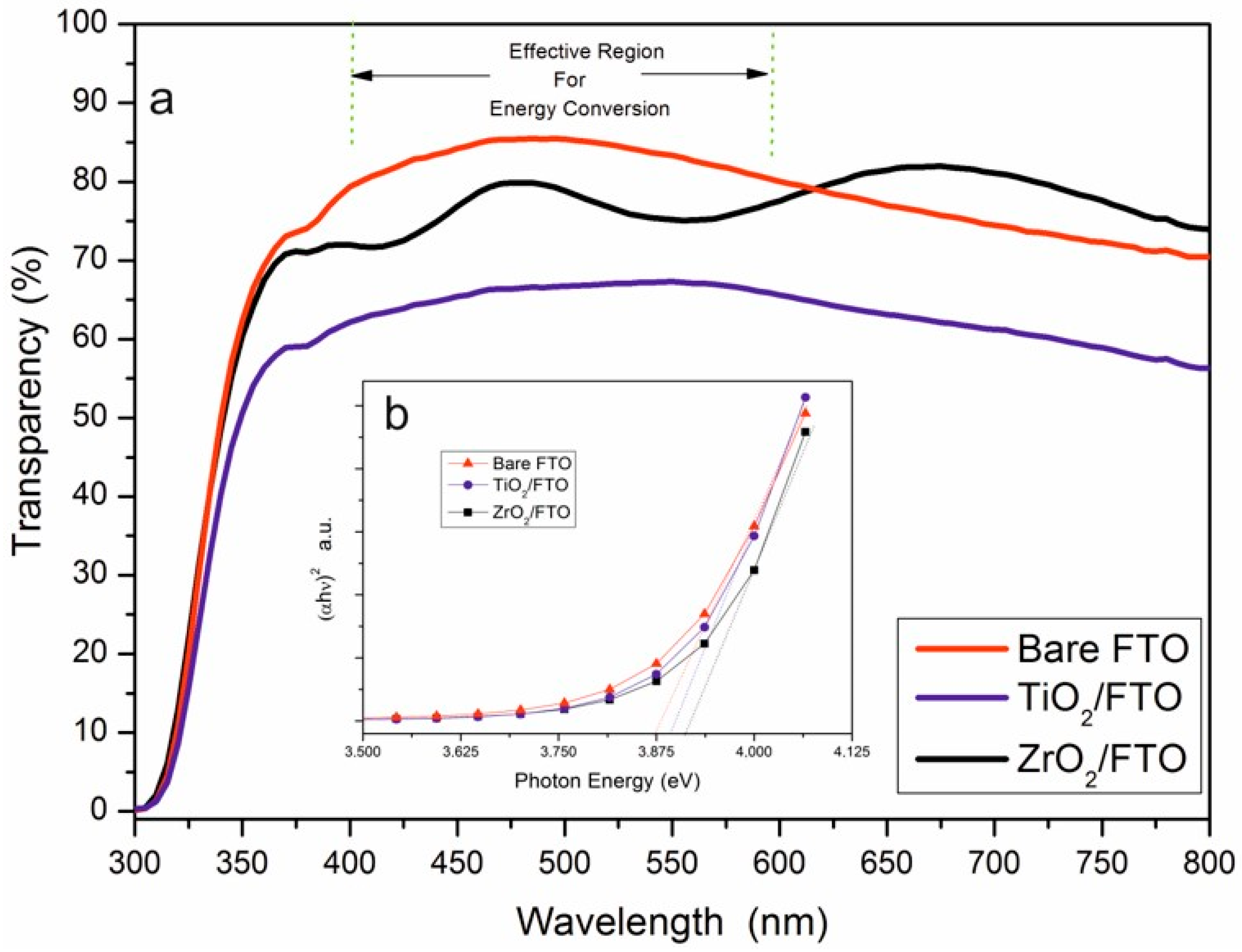
The optical transmittance of the bare and modified FTO substrates within the visible spectrum (300–800 nm) was evaluated using a UV-1900 UV-Vis spectrometer (Shimadzu UV-1900i Plus, Shimadzu Corporation, Kyoto, Japan) (Figure 4a). In the 300–620 nm region, both coated substrates exhibited slightly reduced transmittance relative to the bare FTO. However, at wavelengths exceeding 620 nm, the ZrO2/FTO configuration demonstrated superior optical transparency. This enhanced transmittance in the longer wavelength regime is highly advantageous, as it maximizes the photon flux reaching the mesoporous TiO2 dye interface, directly augmenting photoelectron generation. Although the FESEM analysis revealed comparable top-view surface morphologies for both electron blocking layers, the significant optical discrepancy observed in the UV-Vis spectra (>620 nm) is not attributed to a non-optimal morphology of the TiO2 reference layer. Instead, this difference originates from the intrinsic physical properties and distinct structural densities resulting from their respective synthesis routes. The TiCl4 hydrolysis method typically yields a denser TiO2 phase with a higher refractive index, which can induce slight parasitic optical scattering and thin-film interference at the FTO interface. In contrast, the hydrothermally deposited ultra-thin ZrO2 layer possesses a different intrinsic refractive index and structural density that effectively minimizes internal reflection and scattering in the longer wavelength regime, thereby preserving superior optical transparency. The direct optical band gaps of the films were determined via Tauc plot extrapolations from the low-wavelength transmission data (Figure 4b).
Figure 4.
(a) UV-Vis transmittance spectra (300–800 nm) and (b) the corresponding Tauc plots showing the linear dependence of αhμ2 on photon energy (E, eV) for bare FTO, 56 nm TiO2/FTO, and 48 nm ZrO2/FTO thin films, The dashed lines indicate the corresponding energy values of 3.875 eV for bare FTO, 3.880 eV for TiO2/FTO, and 3.885 eV for ZrO2/FTO.
The calculated optical band gaps were 3.875 eV for bare FTO, 3.880 eV for TiO2/FTO, and 3.885 eV for ZrO2/FTO. A distinct blue shift in the UV-absorption edge was observed for the ZrO2-modified electrode. It should be noted that these values were calculated directly from the transparency-wavelength graphs. Since the deposited TiO2 and ZrO2 layers are ultra-thin (48–56 nm) compared to bulk materials, these data represent the effective optical thresholds of the composite FTO/EBL stack rather than pristine bulk band gaps. Therefore, these calculated values are highly accurate and fall well within acceptable limits for such specific nanoscale heterostructures.
This widened band gap limits parasitic light absorption by the EBL itself, allowing a greater proportion of the solar spectrum to penetrate into the active layer [26]. According to the Burstein–Moss effect, this blue shift indicates a displacement of the surface Fermi level toward higher energy states due to the occupation of lower conduction band levels [27,28].
3.3. Photovoltaic Performance (J-V Characteristics)
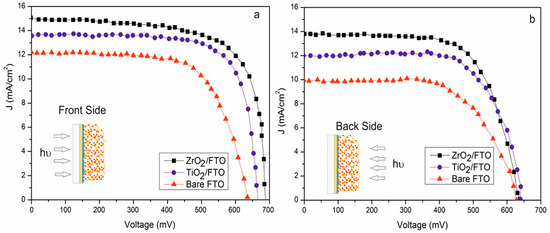
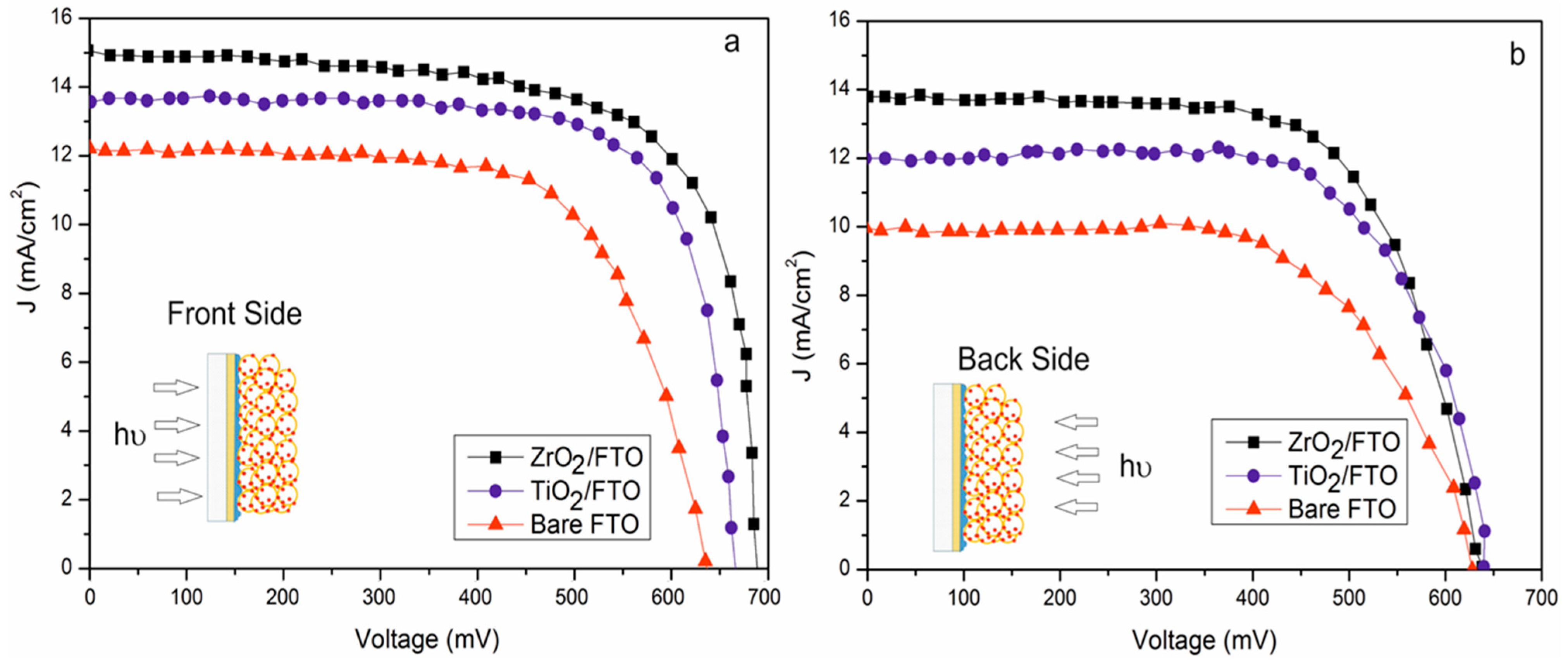
Photocurrent density–voltage (J-V) profiles of the fabricated DSSCs were acquired under simulated AM 1.5 illumination (100 mW/cm2) (Figure 5). Table 1 summarizes the corresponding photovoltaic parameters under both front and back illumination configurations. The data presented in Table 1 correspond to the mean values and standard deviations derived from the five independent samples, whereas the J-V curves displayed in Figure 5 illustrate the performance of the representative champion cells for each configuration. The integration of the ZrO2 blocking layer resulted in a remarkable 43.9% enhancement in overall power conversion efficiency (η) under front illumination. For context, conventional compact layer depositions typically yield efficiency improvements ranging from 30% to 53% [29,30,31]. The concurrent increases in short-circuit current density (Jsc), open-circuit voltage (Voc), and η for the modified cells suggest the effective suppression of interfacial charge recombination.
Figure 5.
J-V curves of DSSCs employing bare FTO, ZrO2/FTO and TiO2/FTO layers electrodes with front (a) and backside (b) illumination (AM 1.5, 100 mW/cm2). The arrows indicate the direction of irradiation.
Table 1.
Efficiency analysis of DSSCs employing bare FTO, ZrO2/FTO and TiO2/FTO layer electrodes with front and backside illumination.
Specifically, the ZrO2-based DSSC achieved an η of 6.77%, outperforming the TiO2-based cell (5.72%) and the bare FTO reference (4.71%). Interestingly, the beneficial effects of the ZrO2 compact layer extended to backside illumination. Under this configuration, the Jsc of the ZrO2/FTO cell decreased by only 8.79%, whereas the bare FTO and TiO2/FTO cells experienced severe reductions of 11.49% and 16.46%, respectively. This superior retention of photocurrent can be attributed directly to the higher optical transmittance and the aforementioned Fermi level shift induced by the ZrO2 layer. Furthermore, the Voc improved from 640 mV (bare FTO) to 660 mV (TiO2) and 680 mV (ZrO2), underscoring the efficacy of ZrO2 in mitigating back-electron transfer dynamics. This upward shift in the effective surface Fermi level at the FTO/ZrO2 interface is fundamentally responsible for the enhanced charge extraction, which is clearly corroborated by the substantial increase in photovoltaic parameters observed under both front and backside illumination modes.
3.4. Incident Photon-to-Current Conversion Efficiency (IPCE)
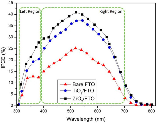
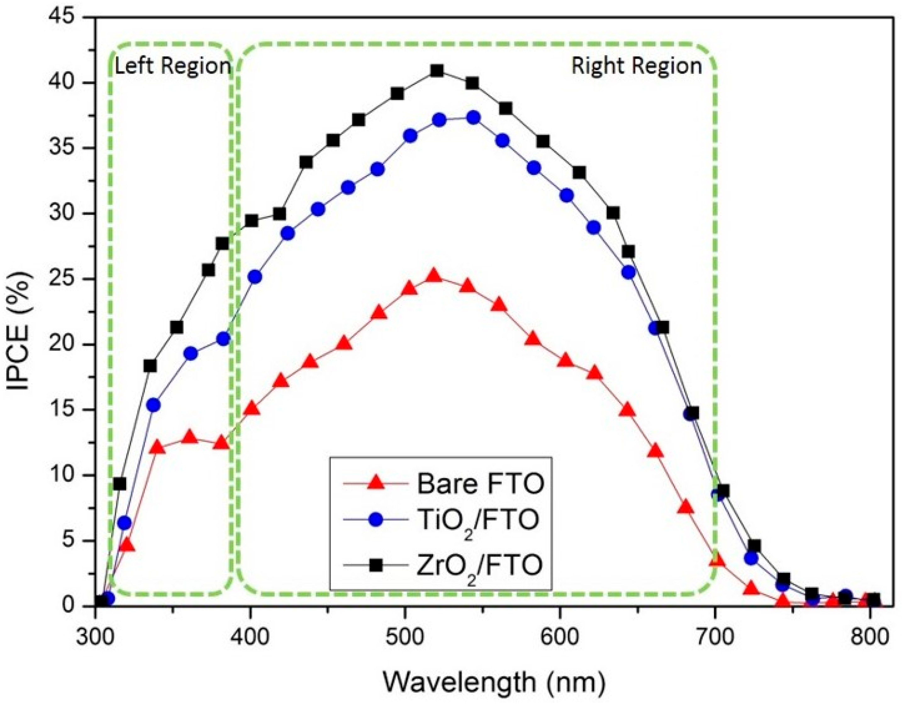
The IPCE spectra (Figure 6) which mathematically represent the External Quantum Efficiency (EQE) of the solar cells, elucidate the quantum efficiency of the devices and strongly correlate with the optical transmittance behavior. In the short-wavelength regime (below 390 nm), a minor peak near 370 nm is discernible for the TiO2-coated FTO, corresponding to the intrinsic bandgap absorption of the TiO2 nanoparticles [32]. Due to the lower molar extinction coefficient here, the dye sensitization effect is minimal. Conversely, the N719 dye dictates the spectral response in the visible region [33]. Notably, the ZrO2/FTO cell exhibited a distinct spectral peak at 420 nm, representing a beneficial red-shift compared to the bare FTO response, which translates to enhanced light harvesting [30]. The primary sensitization peak for N719 was prominently observed at 550 nm [34]. The device utilizing the ZrO2 EBL achieved a peak IPCE of 39%, significantly surpassing the 23% yielded by the bare FTO cell. Overall, the implementation of the ZrO2 layer resulted in a 69% relative enhancement in total IPCE, confirming its superior photon-management capabilities. Crucially, the substantial increase in the integrated area under this IPCE (EQE) spectral curve provides direct, independent physical evidence for the enhanced short-circuit current density (Jsc) observed in the J-V measurements (Table 1). This strict mathematical correlation conclusively validates the superior charge collection efficiency facilitated by the ZrO2 barrier.
Figure 6.
IPCE (Incident Photon-to-Current Efficiency) spectra for the DSSCs with and without blocking layers.
3.5. Electrochemical Impedance Spectroscopy (EIS)
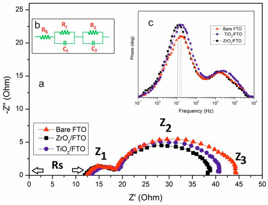
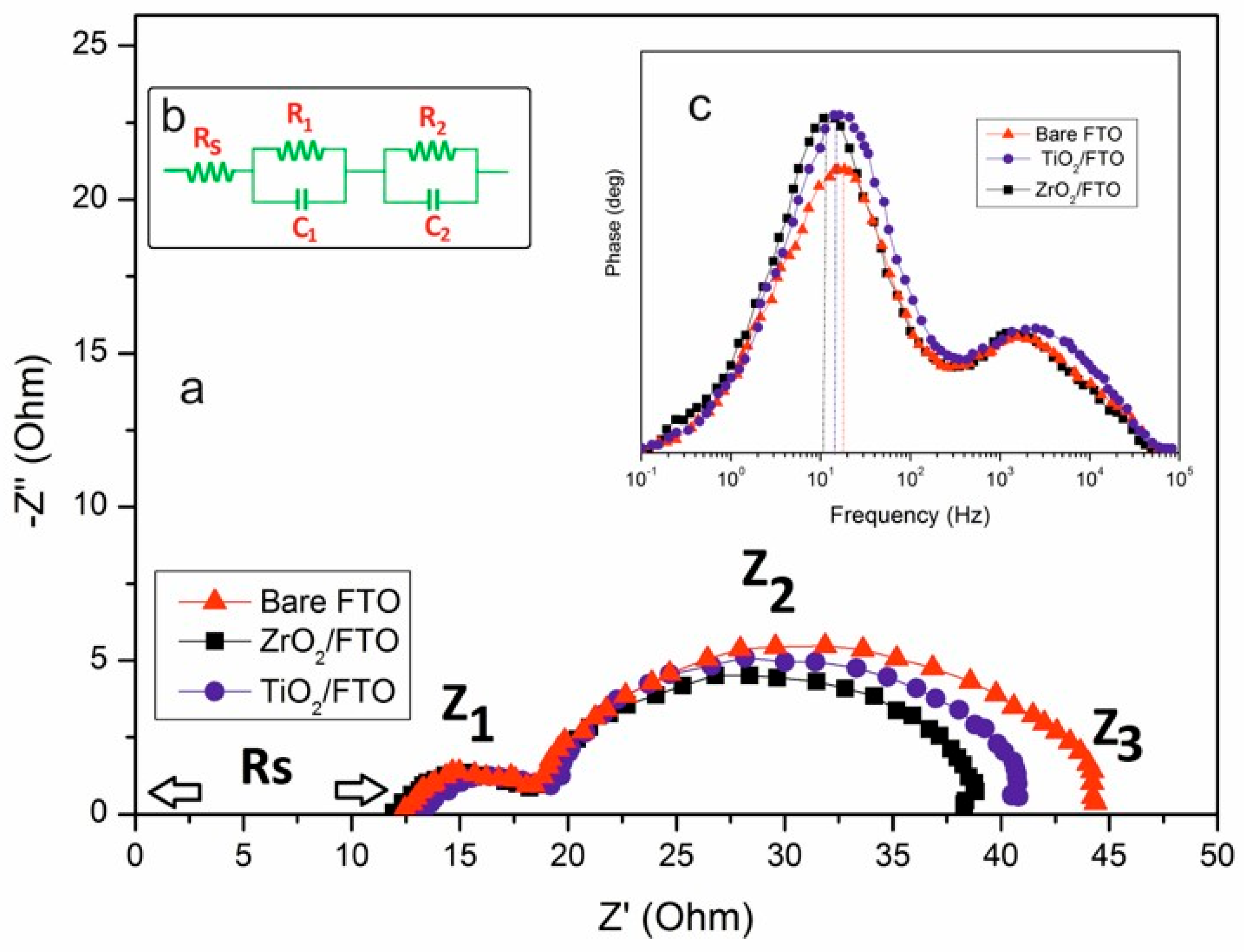
EIS was employed under one-sun, open-circuit conditions to interrogate the interfacial charge transport and recombination kinetics [35,36]. The resulting Nyquist plots (Figure 7a) display two characteristic semicircles across the 10−1 to 105 Hz frequency range. The data were fitted using a standard equivalent circuit model (Figure 7b) [37].
Figure 7.
Representative Nyquist plots displaying impedance data taken at open-circuit potential (a), equivalent circuit of DSSC used for fitting impedance data (b), and Bode plots displaying impedance data (c). The characteristic fmax shifted from 18.49 Hz (bare FTO) to 16.43 Hz (TiO2/FTO) and down to 10.92 Hz for the ZrO2/FTO cell.
The high-frequency element (Rs) represents the sheet resistance of the FTO substrate. The first semicircle (Ω1) reflects the charge transfer resistance (R1) at the conducting substrate/blocking layer/TiO2 and Pt/electrolyte interfaces. The mid-frequency semicircle (Ω2) corresponds to the recombination resistance (R2) at the TiO2/dye/electrolyte interface, while the low-frequency region (Ω3) relates to Nernstian diffusion within the electrolyte [38].
As detailed in Table 2, the ZrO2/FTO architecture exhibited the lowest R1 value, contributing positively to the macroscopic photovoltaic efficiency. More critically, the mid-frequency response provides the electron lifetime (τ), derived from the Bode phase peak frequency (fmax) via the relation [39].
Table 2.
Kinetic parameters of the DSSCs with and without blocking layers.
The characteristic fmax shifted from 18.49 Hz (bare FTO) to 16.43 Hz (TiO2/FTO) and down to 10.92 Hz for the ZrO2/FTO cell. This corresponds to a significantly extended electron lifetime (τ = 0.0146 s) for the ZrO2 modified device compared to the TiO2 reference (τ = 0.0097 s). The extended electron lifetime, coupled with lower charge transport resistance, definitively proves that the ZrO2 layer provides a robust kinetic barrier against interfacial recombination (electron leakage to the I3− electrolyte).
3.6. Theoretical Validation and Optimization Pathways
The exceptional empirical performance of the ZrO2 EBL is fundamentally governed by nanoscale thin-film physics. At a measured thickness of 48 nm, the ZrO2 acts as a highly selective physical barrier. Based on the mathematical modeling strategy (Section 2.3), the low quantum tunneling probability T(E) across this 48 nm boundary mathematically confirms that undesirable electron leakage via backward transfer from the FTO to the electrolyte is heavily restricted. The continuity equation models align with the empirical EIS data, demonstrating that this restricted leakage leads directly to the extended electron lifetime (τ = 0.0146 s) and the lower charge transport resistance observed for the ZrO2/FTO configuration.
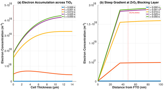
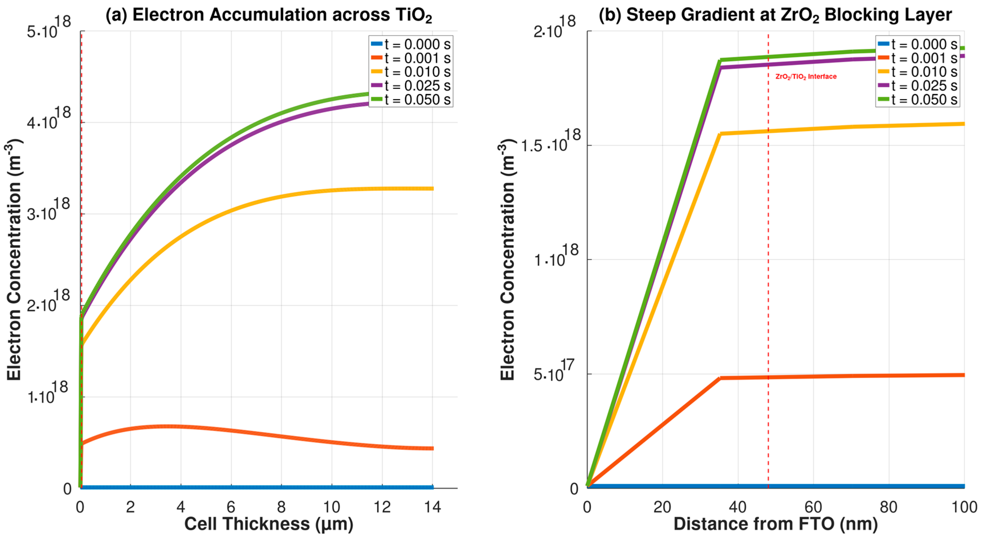
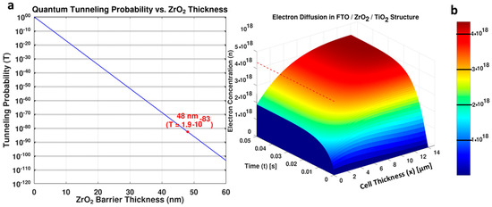
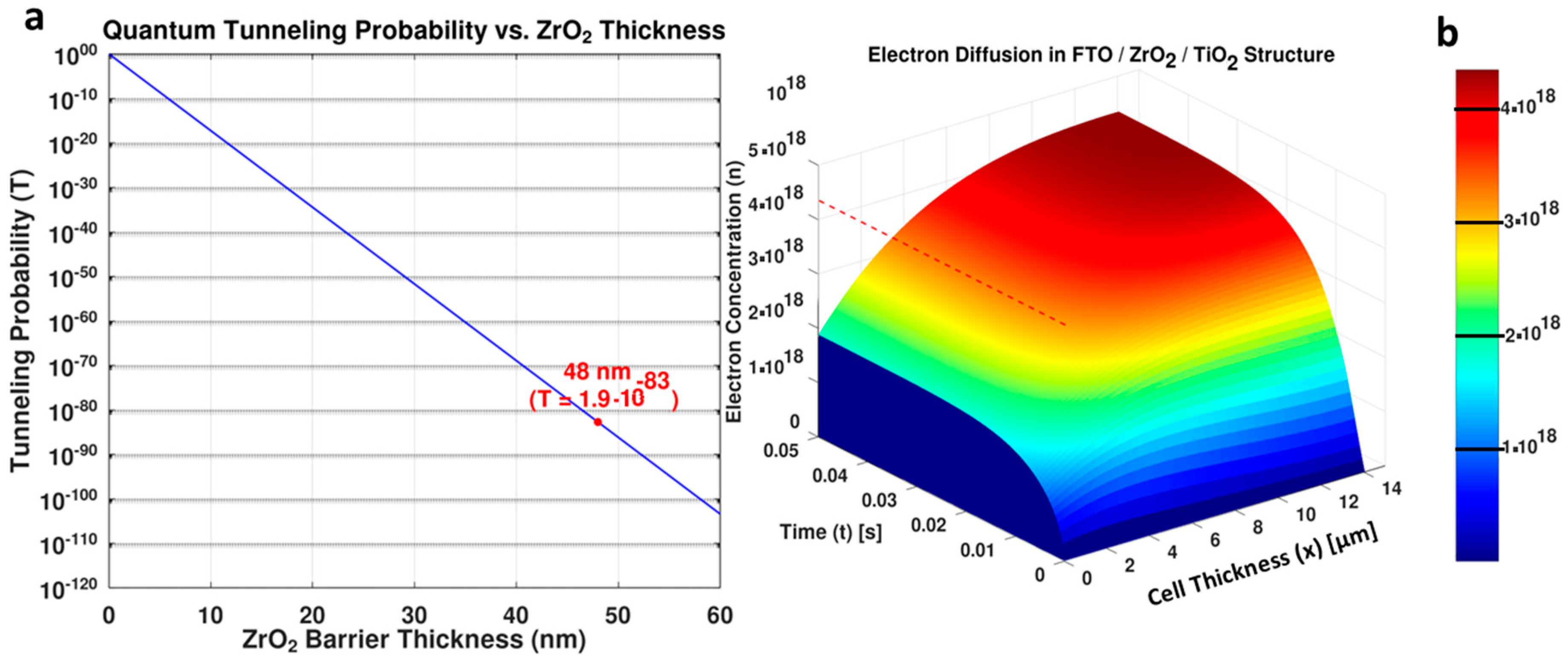
Time-dependent electron diffusion profiles across the photoanode stack simulated via the Crank–Nicolson method. Figure 8a illustrates the rapid accumulation of photogenerated electrons across the 14 µm mesoporous TiO2 network over time, while the magnified interfacial view in Figure 8b highlights the steep concentration gradient established by the ZrO2 blocking layer. This steep gradient visually confirms the layer’s role as a physical barrier, effectively restricting backward electron transfer to the FTO contact as the system reaches a steady state. To theoretically substantiate the barrier properties of the EBL, both the quantum tunneling probability and the spatiotemporal electron dynamics were mathematically simulated. As depicted in Figure 9a, the WKB approximation reveals that a 48 nm ZrO2 layer exhibits a near-zero tunneling probability (T ≈ 1.9 × 10−83). This infinitesimally small value mathematically validates that the ultra-thin ZrO2 film completely quenches quantum tunneling, effectively acting as an absolute physical barrier against reverse electron leakage to the electrolyte. Concurrently, the 3D surface profile derived from the continuity equation (Figure 9b) illustrates a rapid and robust accumulation of photogenerated electrons across the mesoporous TiO2 network. The sustained charge density over time further confirms that the ZrO2 compact layer successfully mitigates recombination losses, thereby maximizing the forward electron flux toward the FTO substrate.
Figure 8.
Time-dependent electron diffusion profiles simulated via the Crank–Nicolson method, illustrating (a) rapid electron accumulation across the 14 µm TiO2 network and (b) the steep concentration gradient established by the ZrO2 blocking layer at the interface.
Figure 9.
Mathematical simulations of the photoanode dynamics. (a) the WKB quantum tunneling probability as a function of ZrO2 barrier thickness, confirming that the experimental 48 nm layer physically prohibits reverse electron leakage (T = 1.9 × 10−83). (b) the 3D spatiotemporal electron diffusion and recombination profile, highlighting robust and continuous charge accumulation across the TiO2 film over time.
Furthermore, the UV-Vis data reveals a blue shift in the optical band gap (from 3.875 eV to 3.885 eV), which, according to the Burstein–Moss effect, indicates that the surface Fermi level shifts toward a higher energy side, favorably aligning the energetics for maximum charge extraction. Looking forward, enriching these validated models with machine learning presents a powerful optimization pathway. Clustering algorithms, such as k-means or DBSCAN, could be applied to analyze the distinct 420 nm IPCE red-shift to mathematically isolate the specific wavelength regions where ZrO2 provides the highest quantum yield. Additionally, while the 48 nm thickness yields a 6.77% efficiency, future implementation of genetic algorithms could interpolate between physical constraints to predict the absolute “perfect” theoretical thickness (e.g., oscillating between 40 nm and 55 nm) to perfectly optimize the balance between optical transparency and electron blocking capability.
4. Conclusions
The pursuit of high-performance solar cells has driven extensive research into interfacial modifications, including solid additives [40] and specifically optimized TiO2 blocking layers [41]. However, this study introduces a fresh perspective to the literature by proving that substituting conventional materials with a wider-bandgap ZrO2 layer creates a far superior, exponentially stronger physical barrier against charge recombination.
In summary, the hydrothermal deposition of a 48 nm ZrO2 blocking layer yields profound enhancements in DSSC performance, establishing it as a highly viable alternative to conventional TiO2 EBLs. The ZrO2 layer optimally shifts the surface Fermi level to facilitate electron extraction, maintains excellent optical transparency. Electrically, it dramatically suppresses the back-electron transfer reaction, extending the electron lifetime and culminating in a 43.9% efficiency enhancement and a 69% IPCE improvement. The fundamental superiority of the ZrO2 blocking layer over conventional TiO2 is governed by its higher conduction band offset and the restriction of conductive trap states. These properties act synergistically to exponentially decrease the reverse tunneling probability, thereby establishing an optimal kinetic barrier against interfacial recombination without hindering forward electron extraction. Crucially, these empirical findings are rigorously validated by mathematical models; quantum tunneling probabilities and recombination kinetics confirm the ZrO2 layer’s function as a selective nanoscale physical barrier rather than a bulk insulator. Future research integrating machine learning algorithms with these mathematical models promises to unlock the absolute theoretical limits of blocking layer thicknesses for next-generation photovoltaics. Future research integrating predictive computational algorithms with these mathematical models promises to unlock the absolute theoretical limits of blocking layer thicknesses for next-generation photovoltaics.
Author Contributions
Conceptualization, H.İ.Y. and M.O.; methodology, H.İ.Y.; software, H.İ.Y.; validation, H.İ.Y. and M.O.; formal analysis, H.İ.Y.; investigation, H.İ.Y.; resources, M.O.; data curation, H.İ.Y.; writing—original draft preparation, H.İ.Y.; writing—review and editing, H.İ.Y. and M.O.; visualization, H.İ.Y.; supervision, M.O.; project administration, M.O.; funding acquisition, M.O. All authors have read and agreed to the published version of the manuscript.
Funding
This research was funded by the Faculty Training Program (ÖYP), and the Middle East Technical University Scientific Research Projects (METU-BAP). Additionally, infrastructural and laboratory support was provided by the Center for Solar Energy Research and Applications (METU-GÜNAM) at Middle East Technical University.
Data Availability Statement
The data presented in this study are openly available in Zenodo at https://doi.org/10.5281/zenodo.22862088.
Conflicts of Interest
The authors declare no conflicts of interest.
References
- O’Regan, B.; Grätzel, M. A low-cost, high-efficiency solar cell based on dye-sensitized colloidal TiO2 films. Nature 1991, 353, 737–740. [Google Scholar] [CrossRef] [Scilit]
- Rahman, S.; Haleem, A.; Siddiq, M.; Hussain, M.K.; Qamar, S.; Hameed, S.; Waris, M. Research on dye sensitized solar cells: Recent advancement toward the various constituents of dye sensitized solar cells for efficiency enhancement and future prospects. RSC Adv. 2023, 13, 19508–19529. [Google Scholar] [CrossRef] [Scilit]
- Rashid, N.Z.; Zaine, S.N.A. Solid-State Electrolyte in Flexible Dye-Sensitized Solar Cells: A Systematic Review. Chem. Methodol. 2026, 10, 123–139. [Google Scholar] [CrossRef]
- Mahadik, S.A.; Pathan, H.M.; Salunke-Gawali, S. An Overview of Metal Complexes, Metal-Free and Natural Photosensitizers in Dye-Sensitized Solar Cells. ES Energy Environ. 2024, 24, 1078. [Google Scholar] [CrossRef] [Scilit]
- Wang, Y.; Wu, W.; Ren, P. Classification, Functions, Development and Outlook of Photoanode Block Layer for Dye-Sensitized Solar Cells. Inorganics 2025, 13, 103. [Google Scholar] [CrossRef] [Scilit]
- Peng, B.; Jungmann, G.; Jäger, C.; Haarer, D.; Schmidt, H.-W.; Thelakkat, M. Systematic investigation of the role of compact TiO2 layer in solid state dye-sensitized TiO2 solar cells. Coord. Chem. Rev. 2004, 248, 1479–1489. [Google Scholar] [CrossRef] [Scilit]
- Sharma, K.; Sharma, V.; Sharma, S.S. Dye-Sensitized Solar Cells: Fundamentals and Current Status. Nanoscale Res. Lett. 2018, 13, 381. [Google Scholar] [CrossRef] [Scilit]
- Liao, Y.-H.; Chang, Y.-H.; Lin, T.-H.; Lee, K.-M.; Wu, M.-C. Recent Advances in Metal Oxide Electron Transport Layers for Enhancing the Performance of Perovskite Solar Cells. Materials 2024, 17, 2722. [Google Scholar] [CrossRef] [Scilit]
- Snaith, H.J.; Schmidt-Mende, L. Advances in Liquid-Electrolyte and Solid-State Dye-Sensitized Solar Cells. Adv. Mater. 2007, 19, 3187–3200. [Google Scholar] [CrossRef] [Scilit]
- Cameron, P.J.; Peter, L.M. Characterization of Titanium Dioxide Blocking Layers in Dye-Sensitized Nanocrystalline Solar Cells. J. Phys. Chem. B 2003, 107, 14394–14400. [Google Scholar] [CrossRef] [Scilit]
- Flores Diaz, N. Interfacial Engineering for Competitive Dye-Sensitized Solar Cells Production. Ph.D. Thesis, Swiss Federal Technology Institute of Lausanne, Lausanne, Switzerland, 2021. [Google Scholar] [CrossRef] [Scilit]
- Yavuz, H.I. Design of High-Efficiency Dye-Sensitized Nanocrystalline Solar Cells (Order No. 31677492). Available from ProQuest Dissertations & Theses Global. (3132860676). 2014. Available online: https://open.metu.edu.tr/handle/11511/23937 (accessed on 31 August 2026).
- Burke, A.; Ito, S.; Snaith, H.; Bach, U.; Kwiatkowski, J.; Grätzel, M. The function of a TiO2 compact layer in dye-sensitized solar cells incorporating “planar” organic dyes. Nano Lett. 2008, 8, 977–981. [Google Scholar] [CrossRef] [Scilit]
- Kumar, N.; Choudhury, S.; Mahajan, A.; Saxena, V. Enhanced efficiency of dye-sensitized solar cells via controlled thickness of the WO3 Langmuir–Blodgett blocking layer in the Debye length regime. Mater. Adv. 2024, 5, 7659–7670. [Google Scholar] [CrossRef] [Scilit]
- Palomares, E.; Clifford, J.N.; Haque, S.A.; Lutz, T.; Durrant, J.R. Control of Charge Recombination Dynamics in Dye Sensitized Solar Cells by the Use of Conformally Deposited Metal Oxide Blocking Layers. J. Am. Chem. Soc. 2003, 125, 475–482. [Google Scholar] [CrossRef] [Scilit]
- Cosar, B.; Icli, K.C.; Yavuz, H.I.; Ozenbas, M. Photovoltaic performance of bifacial dye sensitized solar cell using chemically healed binary ionic liquid electrolyte solidified with SiO2 nanoparticles. Electrochim. Acta 2013, 87, 425–431. [Google Scholar] [CrossRef] [Scilit]
- Icli, K.C.; Yavuz, H.I.; Ozenbas, M. Production of core–shell type conducting FTO/TiO2 photoanode for dye sensitized solar cells. J. Solid State Chem. 2014, 210, 22–29. [Google Scholar] [CrossRef] [Scilit]
- Bisquert, J. Theory of the Impedance of Electron Diffusion and Recombination in a Thin Layer. J. Phys. Chem. B 2002, 106, 325–333. [Google Scholar] [CrossRef] [Scilit]
- Halme, J.; Vahermaa, P.; Miettunen, K.; Lund, P. Device Physics of Dye Solar Cells. Adv. Mater. 2010, 22, E210–E234. [Google Scholar] [CrossRef] [Scilit]
- Varga, Z.; Bobcek, M.; Conka, Z.; Racz, E. Machine Learning-Based Prediction of Dye-Sensitized Solar Cell Efficiency for Manufacturing Process Optimization. Energies 2025, 18, 5011. [Google Scholar] [CrossRef] [Scilit]
- Noh, J.H.; Lee, S.; Kim, J.Y.; Lee, J.-K.; Han, H.S.; Cho, C.M.; Cho, I.S.; Jung, H.S.; Hong, K.S. Functional Multilayered Transparent Conducting Oxide Thin Films for Photovoltaic Devices. J. Phys. Chem. C 2009, 113, 1083–1087. [Google Scholar] [CrossRef] [Scilit]
- Thapa, S.; Paudel, R.; Blanchet, M.; Gemperline, P.T.; Comes, R.B. Probing surfaces and interfaces in complex oxide films via in situ X-ray photoelectron spectroscopy. J. Mater. Res. 2021, 36, 26–51. [Google Scholar] [CrossRef]
- Dragonetti, C.; Colombo, A. Recent Advances in Dye-Sensitized Solar Cells. Molecules 2021, 26, 2461. [Google Scholar] [CrossRef] [Scilit]
- Guittet, M.J.; Crocombette, J.P.; Gautier-Soyer, M. Bonding and XPS chemical shifts in ZrSiO4 versus SiO2 and ZrO2: Charge transfer and electrostatic effects. Phys. Rev. B 2001, 63, 125117. [Google Scholar] [CrossRef] [Scilit]
- Haque, S.A.; Palomares, E.; Cho, B.M.; Green, A.N.M.; Hirata, N.; Klug, D.R.; Durrant, J.R. Charge Separation versus Recombination in Dye-Sensitized Nanocrystalline Solar Cells: The Minimization of Kinetic Redundancy. J. Am. Chem. Soc. 2005, 127, 3456–3462. [Google Scholar] [CrossRef] [Scilit]
- Burnstein, E. Anomalous optical absorption limit in InSb. Phys. Rev. 1954, 93, 632. [Google Scholar] [CrossRef] [Scilit]
- Sernelius, B.E.; Berggren, K.-F.; Jin, Z.-C.; Hamberg, I.; Granqvist, C.G. Band-gap tailoring of ZnO by means of heavy Al doping. Phys. Rev. B 1988, 37, 10244–10248. [Google Scholar] [CrossRef] [Scilit]
- Ito, S.; Murakami, T.N.; Comte, P.; Liska, P.; Grätzel, C.; Nazeeruddin, M.K.; Grätzel, M. Fabrication of thin film dye sensitized solar cells with solar to electric power conversion efficiency over 10%. Thin Solid Films 2008, 516, 4613–4619. [Google Scholar] [CrossRef] [Scilit]
- Kavan, L.; Tétreault, N.; Moehl, T.; Grätzel, M. Electrochemical Characterization of TiO2 Blocking Layers for Dye-Sensitized Solar Cells. J. Phys. Chem. C 2014, 118, 16408–16418. [Google Scholar] [CrossRef] [Scilit]
- Su, T.S.; Hsieh, T.Y.; Hong, C.Y.; Wei, T.-C. Electrodeposited Ultrathin TiO2 Blocking Layers for Efficient Perovskite Solar Cells. Sci. Rep. 2015, 5, 16098. [Google Scholar] [CrossRef] [Scilit]
- Grätzel, M. Dye-sensitized solar cells. J. Photochem. Photobiol. C Photochem. Rev. 2003, 4, 145–153. [Google Scholar] [CrossRef] [Scilit]
- Kojima, A.; Teshima, K.; Shirai, Y.; Miyasaka, T. Organometal Halide Perovskites as Visible-Light Sensitizers for Photovoltaic Cells. J. Am. Chem. Soc. 2009, 131, 6050–6051. [Google Scholar] [CrossRef] [Scilit]
- Hagfeldt, A.; Boschloo, G.; Sun, L.; Kloo, L.; Pettersson, H. Dye-Sensitized Solar Cells. Chem. Rev. 2010, 110, 6595–6663. [Google Scholar] [CrossRef] [Scilit]
- Nazeeruddin, M.K.; De Angelis, F.; Fantacci, S.; Selloni, A.; Viscardi, G.; Liska, P.; Ito, S.; Takeru, B.; Grätzel, M. Combined Experimental and DFT-TDDFT Computational Study of Photoelectrochemical Cell Ruthenium Sensitizers. J. Am. Chem. Soc. 2005, 127, 16835–16847. [Google Scholar] [CrossRef] [Scilit]
- Boschloo, G.; Hagfeldt, A. Characteristics of the Iodide/Triiodide Redox Mediator in Dye-Sensitized Solar Cells. Acc. Chem. Res. 2009, 42, 1819–1826. [Google Scholar] [CrossRef] [Scilit]
- Wang, Q.; Moser, J.E.; Grätzel, M. Electrochemical Impedance Spectroscopic Analysis of Dye-Sensitized Solar Cells. J. Phys. Chem. B 2005, 109, 14945–14953. [Google Scholar] [CrossRef] [Scilit]
- Adachi, M.; Sakamoto, M.; Jiu, J.; Ogata, Y.; Isoda, S. Determination of Parameters of Electron Transport in Dye-Sensitized Solar Cells Using Electrochemical Impedance Spectroscopy. J. Phys. Chem. B 2006, 110, 13872–13880. [Google Scholar] [CrossRef] [Scilit]
- Fabregat-Santiago, F.; Bisquert, J.; Palomares, E.; Otero, L.; Kuang, D.; Zakeeruddin, S.M.; Grätzel, M. Correlation between Photovoltaic Performance and Impedance Spectroscopy of Dye-Sensitized Solar Cells Based on Ionic Liquids. J. Phys. Chem. C 2007, 111, 6550–6560. [Google Scholar] [CrossRef] [Scilit]
- Sze, S.M.; Ng, K.K. Physics of Semiconductor Devices, 3rd ed.; John Wiley & Sons: Hoboken, NJ, USA, 2006; pp. 415–418. [Google Scholar] [CrossRef] [Scilit]
- Sangiorgi, A.; Bendoni, R.; Sangiorgi, N.; Sanson, A.; Ballarin, B. Optimized TiO2 blocking layer for dye-sensitized solar cells. Ceram. Int. 2014, 40, 10727–10735. [Google Scholar] [CrossRef] [Scilit]
- Abbasi, M.S.; Zhang, Z.; Han, Z.; Lv, J.; Wang, S.; Wang, S.; Feng, Y.; Wang, J.; Zhang, G.; Wali, N.; et al. Suppressing Electron–Phonon Coupling via Solid Additives for High-Performance Organic Solar Cells. Aggregate 2026, 7, 70268. [Google Scholar] [CrossRef] [Scilit]

Disclaimer/Publisher’s Note: The statements, opinions and data contained in all publications are solely those of the individual author(s) and contributor(s) and not of MDPI and/or the editor(s). MDPI and/or the editor(s) disclaim responsibility for any injury to people or property resulting from any ideas, methods, instructions or products referred to in the content. |
© 2026 by the authors. Licensee MDPI, Basel, Switzerland. This article is an open access article distributed under the terms and conditions of the Creative Commons Attribution (CC BY) license.