


Abstract
In high-step-up ratio converters for portable battery-powered devices, MOSFET switching loss limits efficiency and thermal design. This paper evaluates a multi-stage adaptive gate driver (MS-AGD) after transfer from a 900 V SiC MOSFET high-step-up converter to a 25 V Si MOSFET transformer-based boost circuit. The MS-AGD detects the Miller plateau by differential sensing and controls gate current in four stages through cascode current mirrors. The target-platform comparison combines measured switching waveforms with a temperature-based coefficient and an apparent indicator under a fixed device, load, fixture, pulse sequence, and thermal path. Total switching energy is not determined directly. Tests at 15 frequency points from 23.26 to 125 kHz show that drain-source voltage reaches its valley in about 500 ns with MS-AGD rather than about 1300–1450 ns with fixed-resistor drive and that the MOSFET package-temperature rise is reduced at all tested points by about 25% on average. The fitted apparent thermal-electrical indicator is also lower. These mutually consistent waveform and thermal results indirectly support a reduced turn-on switching-loss contribution while avoiding interpretation of or apparent as direct measurements of total switching loss or instantaneous channel resistance.
1. Introduction
Flyback and transformer-based boost converters are widely used in portable high-voltage equipment, such as plasma generators and portable medical devices [1,2]. These systems usually raise a 12–48 V battery voltage to several hundred or several thousand volts [3,4]. The voltage gain can reach 20:1 to 100:1 [5]. Under this condition, the switch has high drain-source voltage stress [6]. At the same time, compact products need high power density and high efficiency, so the switching frequency is often increased [7]. As a result, MOSFET switching loss becomes an important design problem [8].
Hard-switching loss is a main barrier to high converter efficiency [9,10]. This problem is more serious when small MOSFET packages are used for compact designs [11]. Their heat-spreading area is small, so a watt-level switching-loss term can cause a fast package-temperature rise [12]. In compact low-wattage (e.g., 5 W) high-step-up systems, switching loss can therefore become a key thermal limit. The main physical reason is the Miller plateau during turn-on [13]. In this stage, is almost constant, while falls. For design analysis, the voltage slew rate can be written as , where is the effective Miller capacitance in the transition range [14]. Since is voltage-dependent, this relation is only used for gate-current design and loss-EMI discussion. It is not used to rebuild the exact measured waveform. A larger gate current can shorten the fall time and reduce switching loss, but it also increases , EMI, ringing, and parasitic excitation.
A fixed gate resistor gives one fixed driving strength during the whole switching process. Thus, it can only give a static trade-off between loss and EMI. Active gate driver (AGD) methods have been proposed to improve this trade-off. They are usually divided into current-source drive, closed-loop feedback control, and multi-stage discrete control [15]. Current-source drivers can control the gate charge process, but they often bring extra cost, area, and power loss [16,17]. Closed-loop drivers can control and in real time, but their delay, sampling resolution, and controller power are not ideal for low-power high-frequency products [18,19,20,21,22,23]. Multi-stage drivers use different gate currents or resistors in different switching stages [24,25]. However, many of them still need calibration at given operating points.
These methods all have limits [26]. A low-cost discrete driver still needs fast response, low hardware cost, and real-time adaptation without calibration. This requires direct sensing of the Miller plateau from the MOSFET switching process instead of relying on digital sampling or pre-calibrated timing.
Existing active gate drivers provide different trade-offs. Current-source drivers offer controlled gate charging but require additional analog hardware and may introduce driver loss [16,17]. Closed-loop or drivers provide real-time regulation but require high-bandwidth sensing and control, increasing delay, complexity, and controller power [18,19,20,21,22,23]. Multi-level discrete drivers reduce the digital-control burden but often rely on preset timing or operating-point calibration [24,25]. The present MS-AGD uses analog sensing and dual thresholds to identify the Miller interval without high-speed digital sampling or timing calibration. Its intended advantage is low-cost event-based adaptation, not universal superiority in loss reduction. Because published gate drivers use different devices, voltage levels, topologies, and loss definitions, their reported percentages cannot be compared directly. The fixed gate resistor is therefore retained as a stable controlled baseline in this experiment; same-platform experimental comparison with other active gate drivers remains future work.
Our previous MS-AGD detects the Miller plateau by differentiation and dual-threshold comparison. It then generates a four-stage gate current with cascode current mirrors. It was first tested on a 5 W, 24–800 V flyback platform, where it reduced switching loss by about 30% and reached 94.5% full-load efficiency. However, that test used one topology and one device group. Its use on other devices and circuit platforms still needs verification (more details are given in the Supplementary Material). Our previous thermal measurement work also introduced and the coefficient [27]. It used the relation between temperature rise and current integral to evaluate MOSFET loss under transformer load. That work showed that transformer parasitic impedance can greatly increase the equivalent switching resistance. The present paper tests whether the same method can compare different gate-drive schemes.
Compared with our previous work, the present study focuses on three new aspects. First, it provides cross-platform feasibility validation of the MS-AGD by transferring the previously reported scheme from a 900 V SiC MOSFET high-step-up converter to a 25 V Si MOSFET transformer-based boost circuit. Second, it develops the device- and platform-specific adaptation required for this transfer, including redesign of the staged gate-current setpoints and Miller-plateau detection parameters for the different gate charge, voltage swing, package, and load characteristics. Third, it applies the -coefficient-based loss-comparison method to evaluate fixed-resistor and MS-AGD operation on the same temperature-controlled platform over 15 frequencies from 23.26 to 125 kHz and relates the observed waveform and thermal-indicator improvements to the resonance behavior of the transformer circuit. Thus, the novelty of this work lies in cross-platform feasibility validation, migration of the gate-drive scheme from SiC to Si MOSFET hardware, and -based comparative loss evaluation, rather than in proposing the MS-AGD topology itself.
2. Theoretical Background
2.1. Equivalent Switching Resistance () and the Coefficient
During MOSFET switching, the transient drain-source resistance can be much larger than the steady on-resistance [28,29]. is defined as the current-squared weighted average of during conduction:
where is the conduction time and is the drain current. In this paper, is obtained by offline integration of over the same conduction window and pulse sequence. Under transformer load, the high- interval overlaps with nonzero . This increases the weighted average resistance and makes higher than that under resistive load [27].
For two drive methods tested with the same device, fixture, and thermal path, an energy-balance approximation can link electrical stress to the measured package temperature rise:
where are the effective thermal capacitance and the equivalent thermal mass of the measured package and sensor path, and is the package-surface temperature rise. This relation is used only for equivalent comparison. It does not assume that all loss is switching loss or that the process is adiabatic. The coefficient is defined as:
Then, the relationship between and can be simplified as:
where accounts for residual thermal offsets in the fixed test protocol. The coefficient is calculated from the slope of the measured relationship, with units of K/(A2·s), and therefore quantitatively describes how the device temperature rise changes with the integrated current-squared stress under the same device, load, fixture, pulse sequence, and thermal path. In physical terms, represents the device temperature rise per unit current stress; a smaller indicates a lower thermal response for the same . Once has been calibrated for a given packaged device and test configuration, the measured current integral can be used to approximately estimate the corresponding package-temperature rise through . This makes useful when direct observation of internal loss or junction temperature is difficult after packaging because comparative thermal behavior can be evaluated from externally measurable current and package-temperature signals. In this paper, and the apparent derived from it are used only as relative comparison indicators under fixed conditions and are not interpreted as direct measurements of instantaneous channel resistance. Further methodological details are provided in the Supplementary Material.
Direct determination of total switching energy would require deskewed integration of over the switching interval or an independent calorimetric loss separation, neither of which is performed in this study. Instead, shortening of the measured high-/nonzero- overlap interval, reduction in package-temperature rise, and reduction in the fitted -based apparent indicator are treated as mutually consistent indirect evidence of a reduced turn-on switching-loss contribution. The method does not quantify total or completely separate conduction and switching losses, or establish target-platform system efficiency.
2.2. Operating Mechanism and Limitations of Fixed Gate Resistor Drive
The fixed gate resistor drive is the most common MOSFET drive method in boost circuits. A PWM signal is amplified by an isolator and a gate-driver IC. The driver then charges and discharges the MOSFET gate through one fixed resistor , usually 2–20 Ω [13,14]. This method is simple, low-cost, and easy to use. Its main limit is that all switching stages use the same . The gate time constant is fixed during turn-on. Therefore, the driver cannot give different currents to different switching stages [15,24].
The MOSFET turn-on process has four stages, and each stage needs a different gate-current level. A small gives fast switching and lower loss, but it can cause high , EMI, and ringing. A large reduces EMI but extends the Miller plateau and increases loss [10,29]. The Miller-plateau duration changes with input voltage. Thus, one fixed cannot stay optimal over a wide operating range.
Therefore, the gate current should be changed with time and matched to each switching stage.
2.3. Operating Principle of the MS-AGD
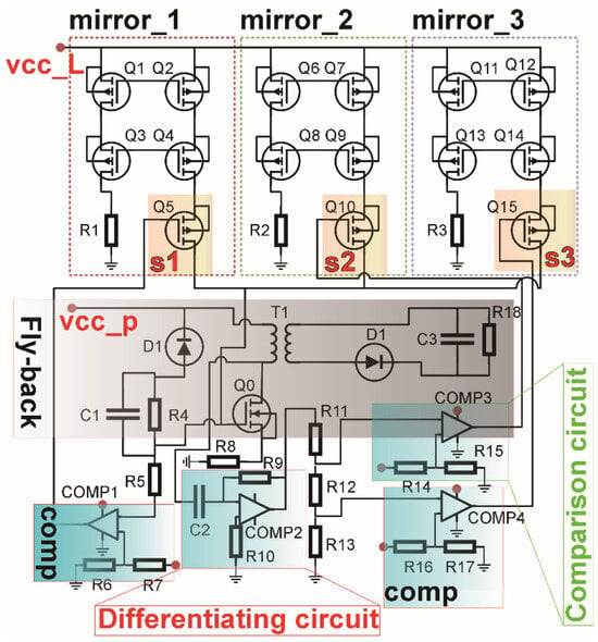
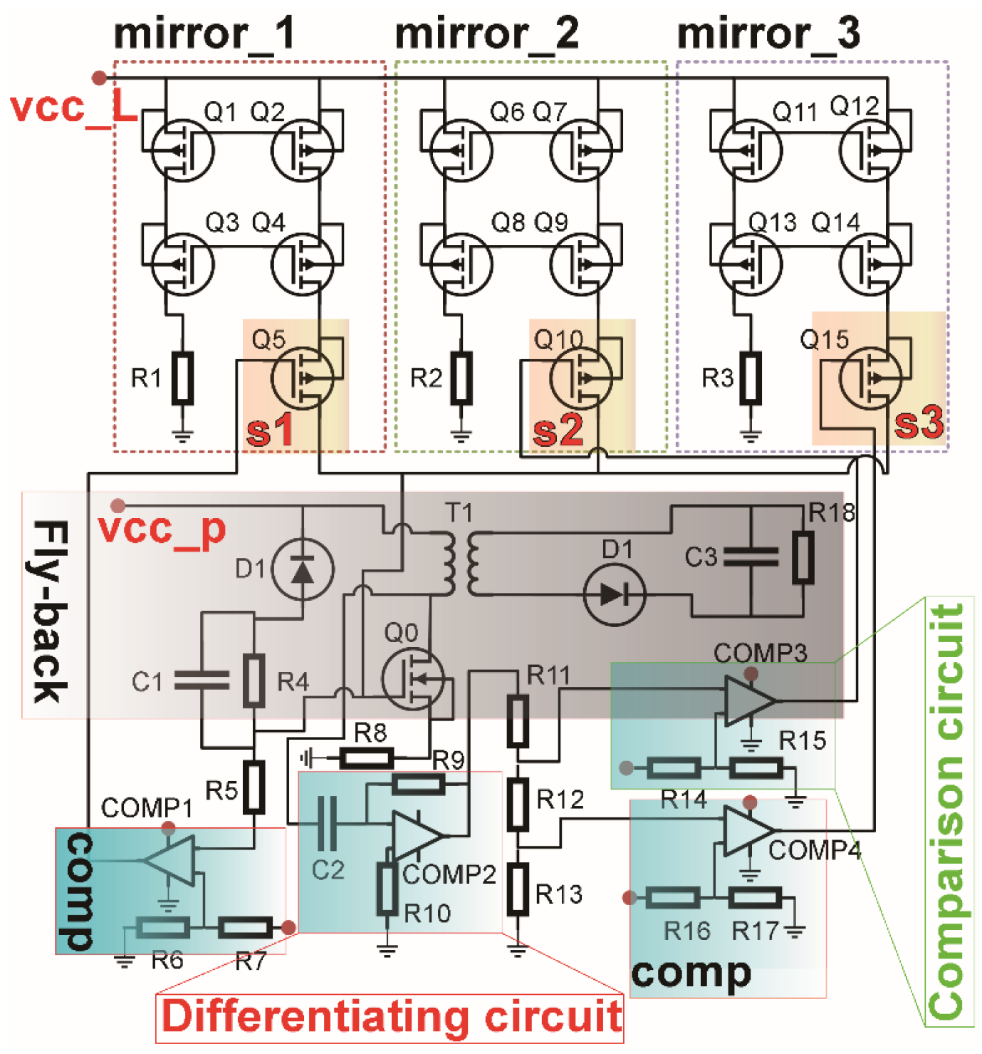
The MS-AGD uses three main mechanisms to reduce switching loss and control EMI. First, it detects the Miller plateau in real time. A band-limited differentiator extracts , and an added RC filter reduces high-frequency noise before the comparator input. Since the differentiator response follows , the threshold relation changes with the operating condition. A dual-threshold comparator detects the start and end of the Miller plateau at 90% and 10% of the peak value, respectively. Second, it controls the gate current in four stages. Three cascode current mirrors provide different gate currents for the turn-on delay, current rise, Miller plateau, and enhanced conduction stages. Figure 1 shows the MS-AGD circuit topology. The upper part is the current-mirror block, and the lower part is the differentiator and comparator block. Third, the circuit is fully discrete. It uses common components, has relatively low hardware cost, and can receive a standard PWM enable signal without firmware changes.
Figure 1.
Circuit topology of the MS-AGD. The upper dashed box contains three sets of cascode current mirrors (mirror_1 to mirror_3), each consisting of four transistors, and one enable switch (S1–S3), providing independent gate-drive currents. The lower-left part is the differentiator circuit (capacitor C2 and the resistor network), which performs time-domain differentiation on to extract the signal. The lower-right part is the comparison circuit, which calibrates the entry and exit of the Miller plateau in real time through dual-threshold discrimination.
3. Experimental Setup
3.1. Platform Differences and Adaptation Strategy
This paper adapts the MS-AGD from the original high-step-up converter platform to the target transformer-based boost circuit. The original platform uses a 900 V SiC MOSFET C3M0065090D (Wolfspeed, Inc., Durham, NC, USA), while the target boost circuit uses a 25 V Si MOSFET BSC670N25NFS3 (Infineon Technologies AG, Neubiberg, Bavaria, Germany). Because the device type, voltage rating, and load are different, the gate-current setpoints and detection parameters must be adjusted. The load circuit and the temperature-measurement platform are kept unchanged. Table 1 compares the main device parameters. The largest difference is the voltage rating. The BSC670N25NFS3 has a much smaller swing than the C3M0065090D, so the differentiator output is also smaller. The two devices still have useful common features. Their Miller-plateau voltages are close, both are N-channel enhancement MOSFETs, and the detection principle does not depend on a specific device model.
Table 1.
Comparison of key parameters between the two MOSFET devices.
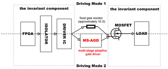
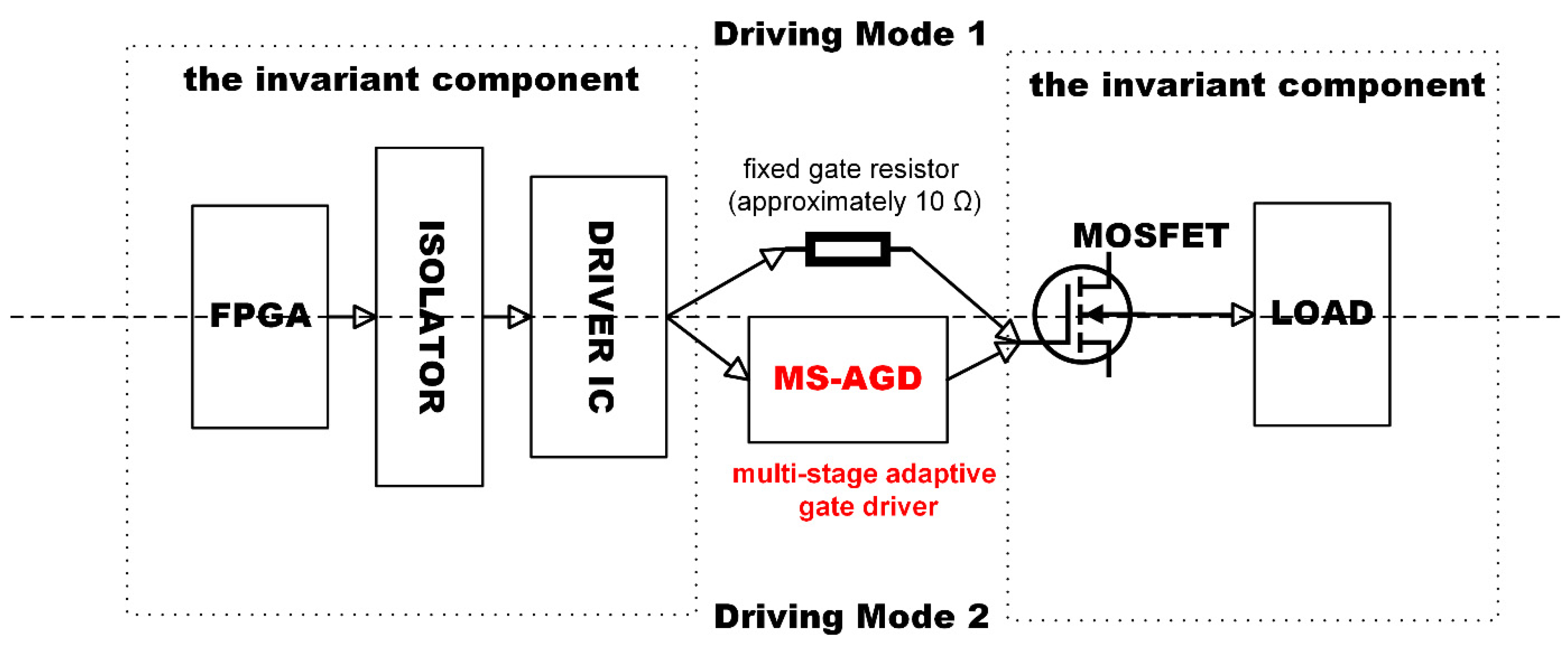
The adaptation follows a minimum-change rule. The transformer load board and the temperature-controlled measurement system are kept the same. Only the front-end gate-drive stage is replaced. Figure 2 shows the replacement scheme.
Figure 2.
Replacement scheme for the MS-AGD in the transformer-based boost circuit. In Mode 1, the FPGA outputs a PWM signal through an isolator and a power driver IC and drives the MOSFET gate through a fixed gate resistor (approximately 10 Ω). In Mode 2, the output of the power driver IC serves as the enable signal for the MS-AGD, and the three sets of cascode current mirrors take over the gate charging process.
3.2. MS-AGD Parameter Optimization
The calculations in this subsection are first-order design estimates used to select the current and detection parameters. They provide design guidance only; experimentally verified switching behavior is presented in Section 4.
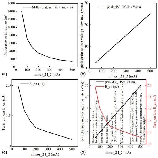
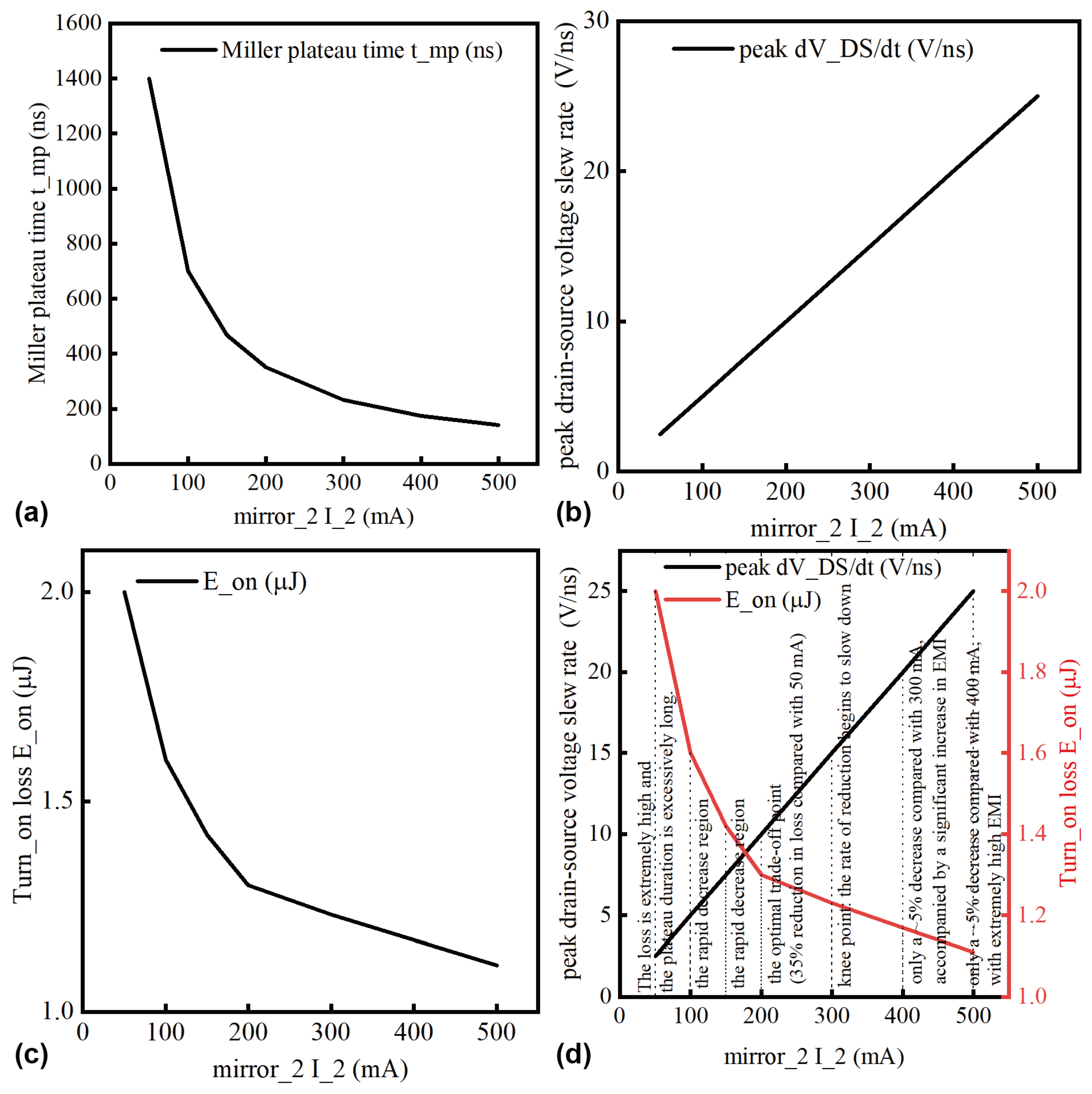
More specifically, , , the sweep in Figure 3, and the ideal LTspice timing in Figure 4 are analytical design guidance. They are used to select the initial , , and comparator thresholds, but and are not treated as measured quantities. In the actual transformer circuit, leakage inductance , inter-winding capacitance , , loop damping, PCB noise, and other circuit parasitics modify the plateau duration and waveform shape. Their combined influence is therefore evaluated from the measured , , and waveforms in Figure 5, Figure 6 and Figure 7. These measurements confirm the functional adequacy of the selected through the observed 300–400 ns Miller plateau and the approximately 500 ns fall to its valley and confirm the functional adequacy of through correct stage transitions at 76.92, 100, and 125 kHz. The temperature-controlled and results provide the comparative thermal validation. Thus, the analytical quantities guide parameter selection, whereas the measured waveform and thermal data establish performance under the actual parasitic network.
Figure 3.
MATLAB (R2024a) parameter sweep for mirror_2 current. (a) The Miller-plateau duration. (b) Peak . (c) Turn-on loss . (d) The joint and trade-off. The selected value is 200 mA.
Figure 4.
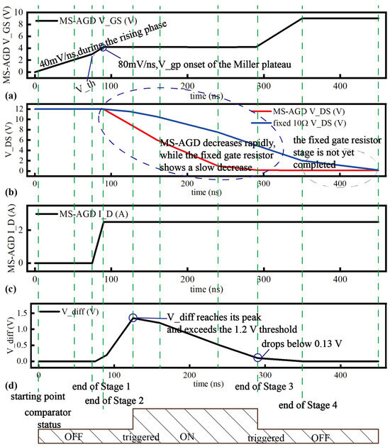
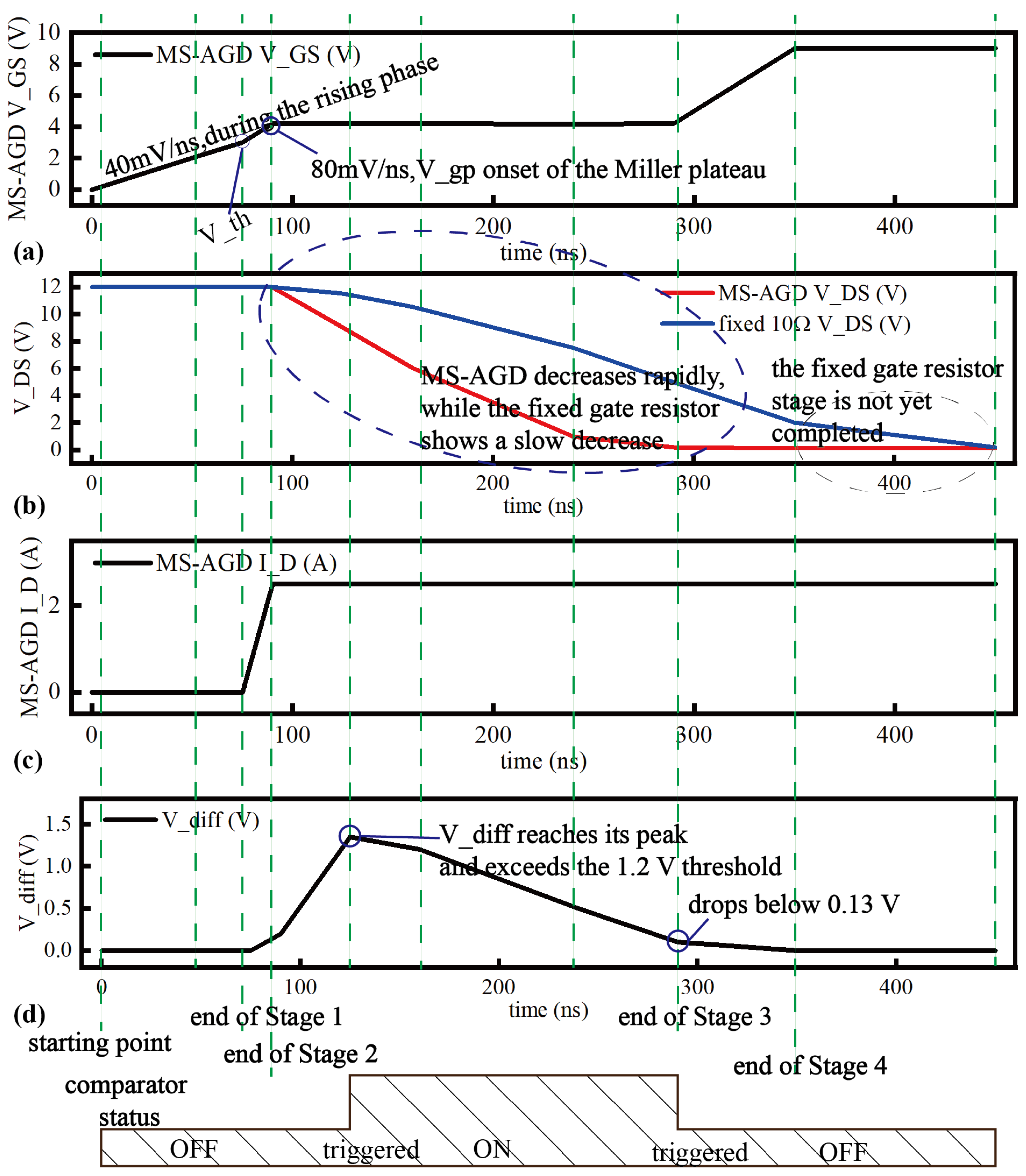
Ideal LTspice simulation for MS-AGD design in the transformer-based boost circuit. (a) . (b) . (c) . (d) . The result is used to check the expected timing relation and guide parameter selection.
Figure 5.
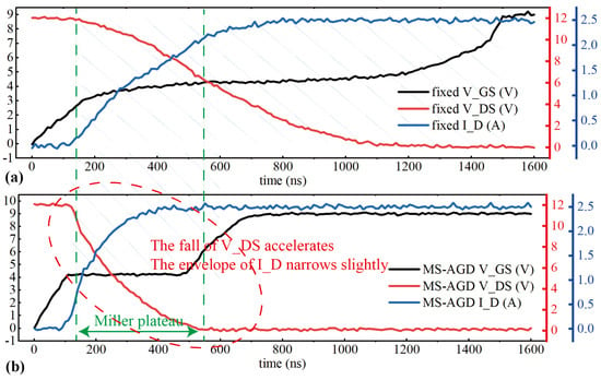
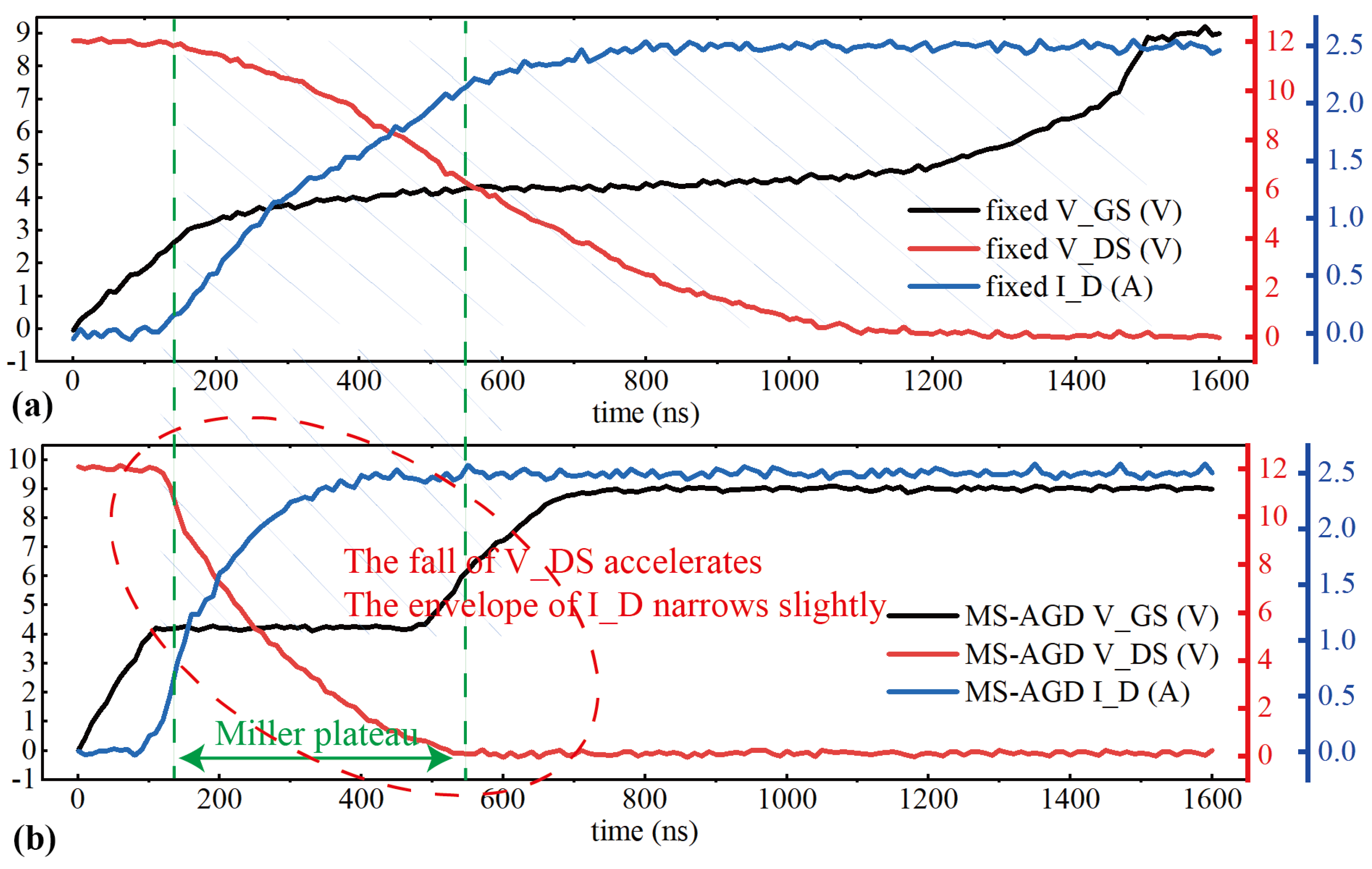
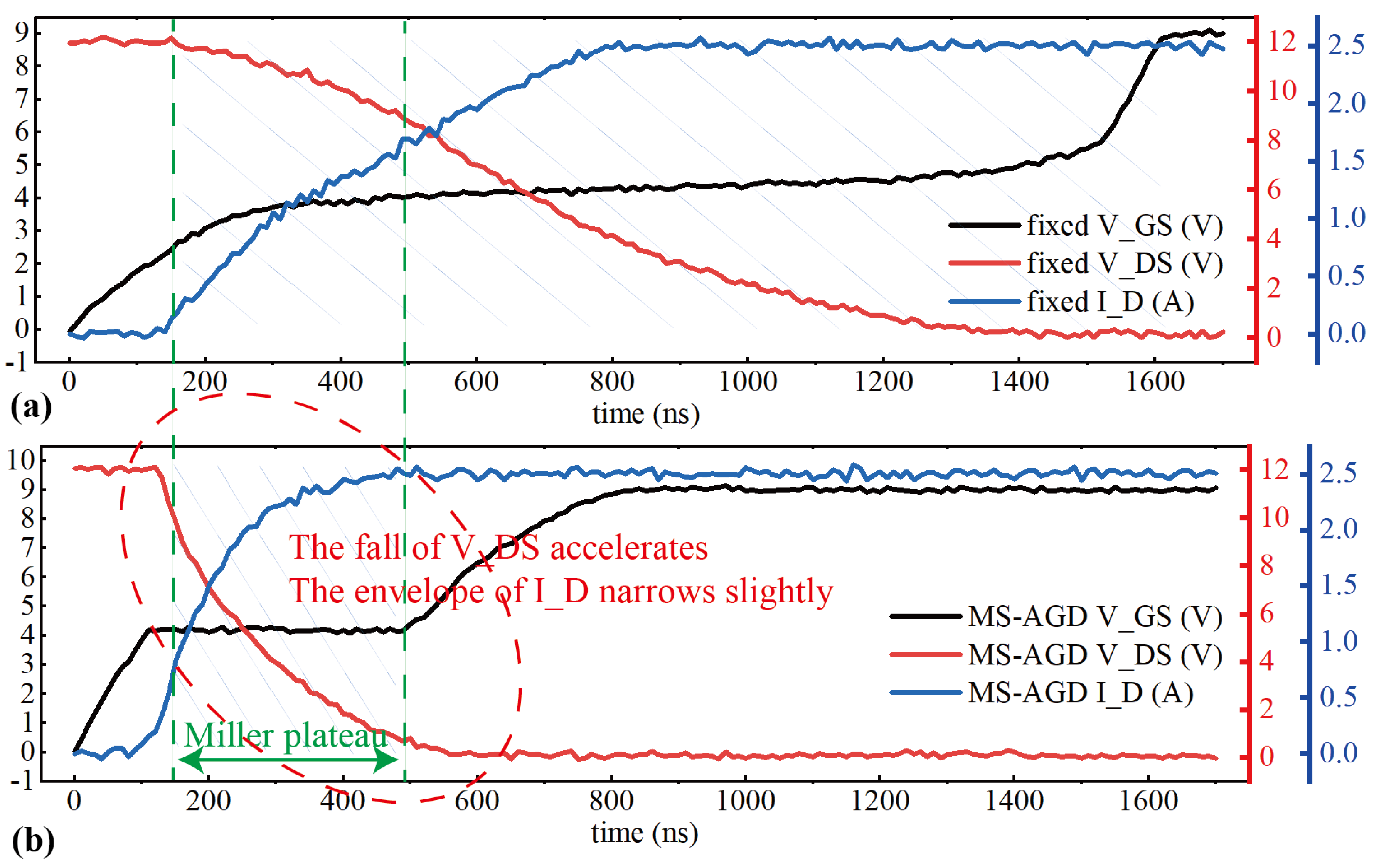
Measured MOSFET switching waveforms at 76.92 kHz. (a) Fixed-resistor drive; (b) MS-AGD drive. The annotations identify the Miller interval and valley. The main comparison is a reduction in the transition from approximately 1300 ns to approximately 500 ns; detailed stage interpretation is given in the text.
Figure 6.
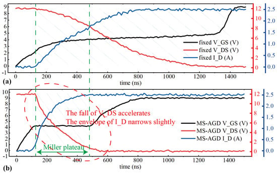
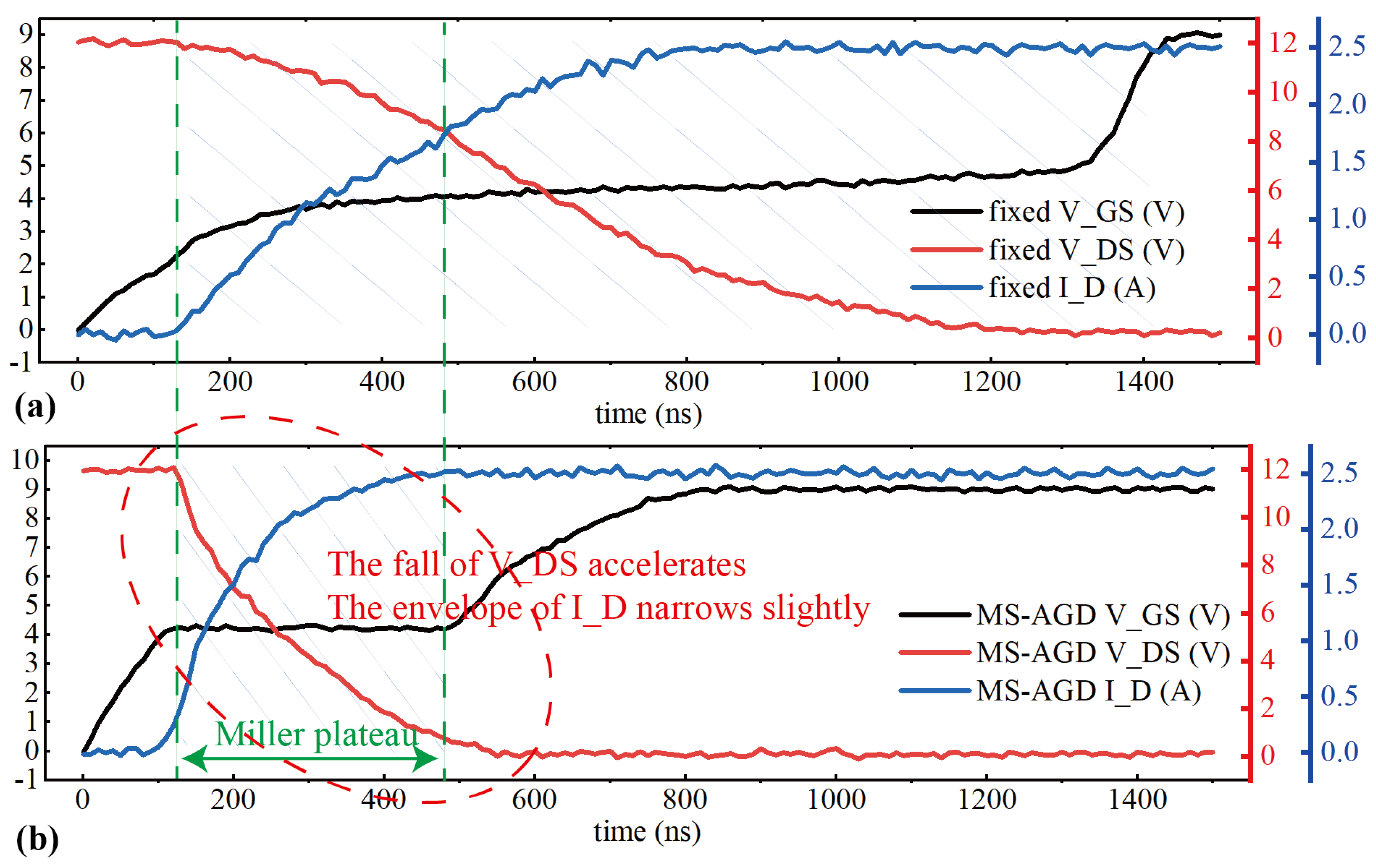
Measured MOSFET switching waveforms at 100 kHz. (a) Fixed-resistor drive; (b) MS-AGD drive. The transition decreases from approximately 1400 ns to approximately 500 ns, while the measured four-stage behavior is retained.
Figure 7.
Measured MOSFET switching waveforms at 125 kHz. (a) Fixed-resistor drive; (b) MS-AGD drive. The transition decreases from approximately 1450 ns to approximately 500 ns, reducing its share of the 4 μs conduction window from about 36% to about 12.5%.
The current setpoints were redesigned for the BSC670N25NFS3. For mirror_1, which is used in Stages I and II, the current is set to 50 mA. With at , the rise rate is:
needs about 70 ns to rise from 0 V to the threshold voltage of about 3 V. This lower slew rate helps reduce gate-trace EMI and crosstalk during turn-on delay. For mirror_2, which drives the Miller plateau, the current is set to 200 mA. The first-order estimate is , which gives about 40 ns when is 8 nC. In the transformer circuit, leakage inductance , inter-winding capacitance , , and loop damping extend the actual plateau. Figure 3 shows the MATLAB sweep used to choose . When increases from 50 mA to 200 mA, decreases by about 35%. A further increase mainly raises and EMI risk. Thus, 200 mA is selected as the loss-EMI compromise. For mirror_3 (Stage IV drive current, i.e., the enhanced conduction stage), the setpoint current . The charge required in this stage is approximately , and the charging time required at a current of 150 mA is approximately 67 ns. Moderately reducing the drive current in this stage helps mitigate the voltage overshoot of when entering the overdrive region, thereby reducing the electrical stress on the gate oxide layer.
The differentiator parameters also need adjustment. Under 12 V input and about 200 ns Miller-plateau duration, the original parameters give a small ():
This value is too close to the PCB high-frequency noise floor of about 50–100 mV. Increasing to 22 pF raises the expected peak to about 1.32 V. The added RC filter further improves noise immunity. The TLV3601 thresholds are set to about 1.2 V for Miller_Start and 0.13 V for Miller_End [30].
3.3. Ideal-Model LTspice Simulation for Design Guidance
An ideal LTspice model is built to guide the current-mirror and differentiator design. The model checks the timing relation and parameter trend. It is not used to reproduce all hardware non-idealities. Figure 4 shows the simulation result. The simulation gives the expected four-stage waveform and a of about 1.2–1.4 V at Miller-plateau entry. Because the model uses ideal switching elements and lumped parasitic parameters, it does not include all measured ringing, non-monotonic behavior, or noise [31,32]. Accordingly, Figure 3 and Figure 4 are used to establish parameter trends and expected timing, whereas the performance claims in this paper are based on the measured waveforms and temperature-controlled experiments.
3.4. Fixed Gate Resistor Drive Baseline Configuration
The fixed-resistor baseline uses the FPGA signal, a digital isolator, a gate-driver IC, and a 10 Ω gate resistor. The 10 Ω value follows the device application practice and is also the value used in the previous temperature-rise study [27]. Using the same value keeps the two studies comparable. As discussed in Section II-B, the fixed resistor cannot meet the different needs of the four switching stages. It is simple and stable, but it provides only one gate-current level. This makes it a suitable baseline for evaluating the MS-AGD. The previous study [27] gave the full temperature-rise baseline for this fixed-drive case. Under transformer load, the coefficient was 26.15 K/(A2·s), and was about 1.57 Ω. These data are used as the reference for this work.
3.5. Comparative Experiment Design
The experiments use a controlled-variable method. The gate-drive method is the only changed factor. All other conditions are kept the same. The transformer load board includes the BSC670N25NFS3 module, an EF15 transformer, a decoupling module, and a secondary voltage-doubler rectifier with a 0.4 μF load capacitor. The measurement system includes an acrylic enclosure, a programmable chamber at 16 °C, a reference PT1000 sensor, a Keysight 34470A multimeter, current probes with bandwidth above 200 MHz, and digital oscilloscopes. A PT1000 sensor is attached to the MOSFET package with Shin-Etsu X-23-7921-5 thermal compound [27]. As shown in the Supplementary Material, the short-term reference ambient fluctuation in the enclosure is better than ±0.003 K. This value means chamber stability during the measurement window, not the absolute accuracy of the sensor. The frequency sweep uses 15 points from 23.26 to 125.00 kHz. The PWM high-level time is fixed at 4 μs. At each frequency, 15,000 switching cycles are measured. Each test is repeated three times and averaged. The cooling interval between two tests is at least 10 min.
The comparative measurement procedure was carried out in the following order. First, the fixed-resistor configuration was measured as the baseline using the 15-point frequency sweep, a fixed 4 μs PWM high-level duration, 15,000 cycles per point, and three repeated measurements. Second, only the gate-drive module was replaced by the MS-AGD; the device, transformer load board, sensors, fixture, and thermal environment were unchanged. Third, after replacement, the system operated without load for at least 30 min to restore thermal equilibrium. Fourth, the same measurement procedure was repeated for the MS-AGD configuration, with at least 10 min cooling between consecutive tests. The complete comparison was finished within 8 h so that the long-term ambient drift remained within ±0.15 K [33,34].
4. Results
4.1. Switching Waveform Comparison at Multiple Frequency Points
This section compares the switching waveforms at 76.92, 100.00, and 125.00 kHz. These points are used to verify the four-stage drive and the Miller-plateau shortening effect. The oscilloscope average mode is used, so the curves are timing waveforms for comparison, not single-shot noise records.
- (a)
- 76.92 kHz (near the resonance peak, duty cycle 30.77%)
Figure 5 compares the two drive methods at 76.92 kHz. This frequency is close to the resonance peak of the temperature-rise curve and has relatively high current stress.
Under fixed drive, rises as an RC charging curve and shows a Miller plateau near 4.2 V. Because of transformer parasitics, the fall is not smooth and lasts about 1300 ns. The waveform rises slowly and does not form a steady plateau.
Under MS-AGD drive, shows four clear stages. The Miller plateau is shortened to about 300–400 ns, and reaches its valley in about 500 ns. Under fixed drive, the same process takes about 1300 ns. The peak and envelope are close for the two drive methods. The high-frequency oscillation appears in both cases, so it comes mainly from transformer parasitics. The MS-AGD shortens the oscillation duration and reduces its loss contribution.
- (b)
- 100 kHz (high-frequency region, duty cycle 40%)
Figure 6 compares the waveforms at 100 kHz. The duty cycle is 40%, so the switching interval takes a larger part of the total cycle.
At 100 kHz, the MS-AGD still keeps the four-stage drive shape. reaches its valley in about 500 ns with MS-AGD drive and about 1400 ns with fixed drive. Since the duty cycle is higher than at 76.92 kHz, the benefit of a shorter transition becomes more important.
- (c)
- 125 kHz (highest frequency, duty cycle 50%)
Figure 7 compares the waveforms at 125 kHz. This is the highest test frequency, and the duty cycle is 50%.
At 125 kHz, the fall time is about 1450 ns under fixed drive and about 500 ns under MS-AGD drive. Thus, the high-impedance transition interval is greatly shortened. The differentiator and comparator also work normally at this frequency.
The main takeaway from Figure 5, Figure 6 and Figure 7 is that the MS-AGD maintains the intended four-stage operation throughout the representative frequency range while shortening the high-impedance transition. At 76.92 kHz, reaches its valley in about 500 ns with the MS-AGD and about 1300 ns with fixed drive. At 125 kHz, the corresponding times are about 500 and 1450 ns, reducing the transition-time share of the 4 μs conduction window from about 36% to about 12.5%. This shorter overlap between nonzero and high is important because it reduces the interval associated with high transient dissipation.
4.2. Frequency Characteristics of Full-Frequency-Range Temperature Rise and
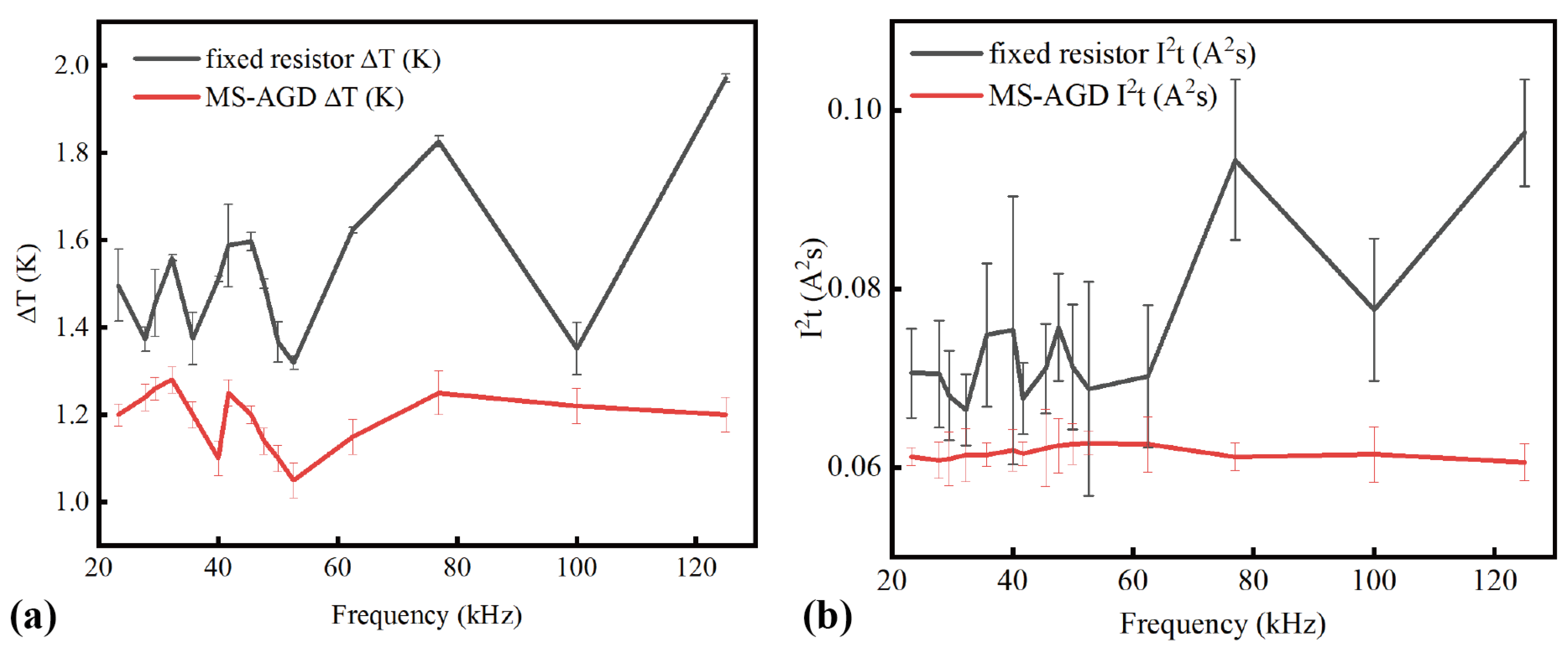
Figure 8 compares the temperature-rise and trends over 23.26–125 kHz.
Figure 8.
Full-frequency-range temperature rise and current integral comparison (23.26–125 kHz, 15 frequency points). (a) –frequency characteristics: the gray curve represents fixed gate resistor drive, and the red curve represents MS-AGD drive. Each data point is the mean of three repeated measurements, and the error bars indicate the standard deviation. The MS-AGD reduces the temperature rise at all 15 frequency points, and the resonance peak and valley positions of the two curves are essentially the same. (b) -frequency characteristics: the under fixed drive fluctuates within the range of 0.07–0.095 A2·s, while the under MS-AGD is concentrated around 0.06–0.063 A2·s, with a significantly reduced fluctuation amplitude, and the resonance peak and valley positions are synchronized with the curve.
The main takeaway from Figure 8 is that the MS-AGD reduces the MOSFET temperature rise at all 15 tested frequencies, with an average improvement of about 25%, while preserving the peak and valley positions of the fixed-drive curve. The common frequency trend indicates that transformer coupling and circuit parasitics mainly determine the resonance pattern, whereas the gate-drive method changes the thermal-loss level at each operating point.
The temperature-rise reduction is larger than the reduction. In the relation , this means that the improvement is associated with both a smaller accumulated current integral and a smaller fitted coefficient. The latter is interpreted as a lower thermal response per unit current stress under the fixed protocol, rather than as a direct measurement of the MOSFET channel resistance.
4.3. Quantification of Equivalent Switching Resistance ()
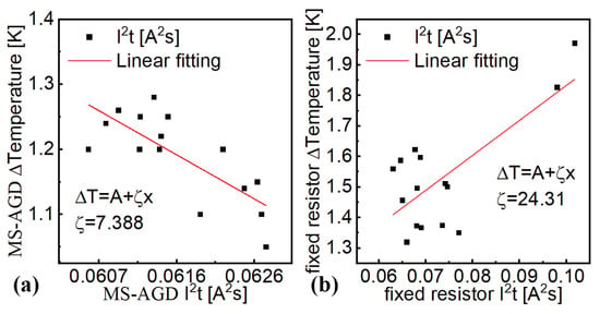
Figure 9 shows the scatter plots and linear fits for the two drive methods.
Figure 9.
scatter plots and linear fitting. (a) MS-AGD drive, with the data of the 15 frequency points distributed near the fitted line, , and the data points concentrated around . (b) Fixed gate resistor drive (baseline remeasurement in this round), (the original value in the prior study was 26.15, with a deviation of approximately 7%, which is within the experimental repeatability range), with data points distributed in the range of . The coefficient is reduced by approximately 70%, indicating that the comprehensive equivalent resistance of the MOSFET under MS-AGD drive is significantly decreased.
Within the measured range, the relation remains consistent under MS-AGD drive. The values shift lower and become narrower than those under fixed drive. This shows that MS-AGD reduces both the current integral and the fitted coefficient.
The local values at 32.26, 50.00, and 100.00 kHz are 7.8, 7.1, and 7.6 K/(A2·s). They agree with the full-range value of 7.39 K/(A2·s) within 10%.
Because is treated as an effective package-and-sensor thermal term rather than independently identified for each test, the values calculated below are reported as apparent comparative indicators. Their numerical difference represents a change in fitted thermal-electrical response under fixed conditions, not a direct measurement of instantaneous channel resistance or total switching energy.
Using the coefficient and the known thermophysical parameters of the BSC670N25NFS3, can be calculated from Equation (3) for the two drive methods:
Fixed drive (remeasured in this study):
MS-AGD:
The reduction in the equivalent switching resistance is:
The reduction rate of the equivalent switching resistance is:
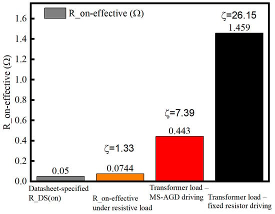
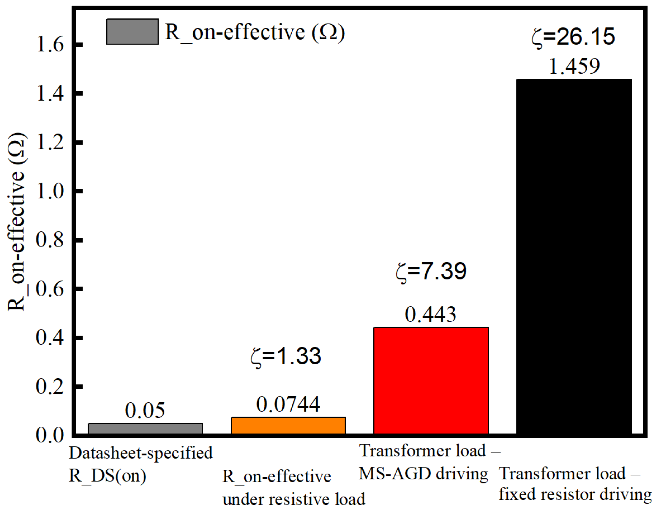
The main takeaway from Figure 10 and Table 2 is the relative separation among the thermal-electrical indicators under different load and drive conditions. Under the fixed measurement assumptions, the apparent decreases from 1.459 Ω with fixed drive to 0.443 Ω with the MS-AGD, a reduction of about 69.6%. The MS-AGD value remains higher than the 74.4 mΩ resistive-load result and the nominal , showing that transformer parasitics remain important. These values are comparative indicators for the fixed protocol and are not direct extractions of instantaneous channel resistance.
Figure 10.
Bar chart comparison of the equivalent switching resistance. From left to right: datasheet nominal (50 mΩ), equivalent resistance under resistive load (74.4 mΩ, ), transformer load with MS-AGD drive (0.443 Ω, ), and transformer load with fixed drive (1.459 Ω, ). The specific values and their multiples relative to the nominal are annotated above each bar. The MS-AGD reduces the equivalent resistance under transformer load by approximately 70%, but the reduced value of 0.443 Ω is still approximately 6 times the equivalent resistance under resistive load.
Table 2.
Comparison of the coefficient and equivalent switching resistance between the two drive methods.
4.4. Full-Frequency-Range Temperature Rise Improvement Rate and Resonance Correlation
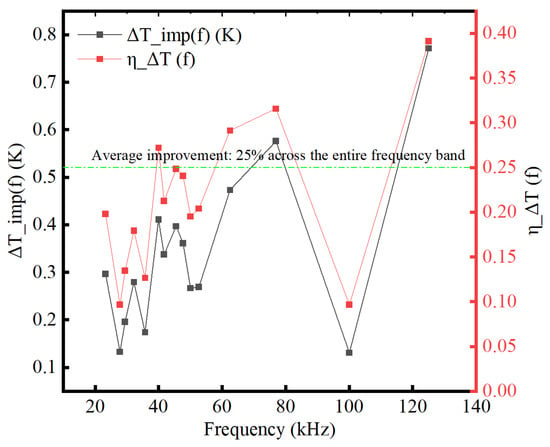
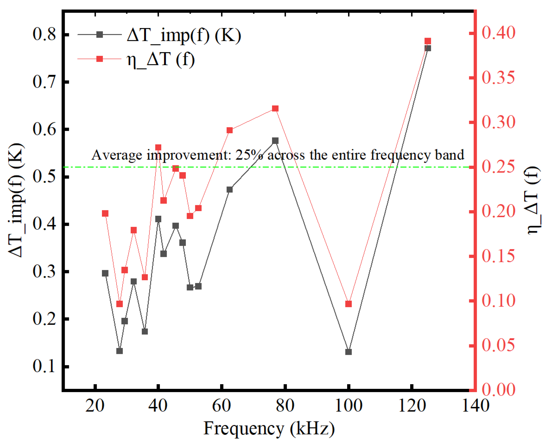
The temperature rise improvement rate is defined as in Equation (11). Figure 11 shows the result at all 15 frequencies.
Figure 11.
Temperature-rise improvement rate versus frequency. The gray line shows the absolute temperature-rise reduction, and the red line shows . The average improvement is about 25%. The improvement is larger near the resonance peak and smaller at lower-loss frequencies.
The main takeaway from Figure 11 is that the temperature-rise improvement is positive at all 15 frequency points, with an average of about 25%. The improvement is larger near the resonance peak, where current stress and the parasitic-transition interval are greater, and smaller at lower-loss operating points. The 125 kHz result confirms operation at the upper end of the tested range but does not establish performance outside the 23.26–125 kHz test band.
5. Discussion
5.1. Physical Mechanism of the Equivalent Switching Resistance Reduction
The decrease in the apparent is mainly associated with the shorter high-resistance transition in Equation (1). The 200 mA Stage-III current shortens the measured Miller plateau from about 800–1200 ns under fixed drive to about 300–400 ns under MS-AGD drive, thereby reducing the interval in which nonzero overlaps with high [35,36]. The 50 mA current in Stages I and II limits excessive , while the 150 mA Stage-IV current completes gate charging after the plateau [37]. Because the function of each stage is described in Section II-C, it is not repeated here. Overall, Stage III provides the primary reduction, and the other stages support a controlled transition [38].
5.2. Methodological Significance of the Coefficient Method
The coefficient is used as a relative evaluation tool, not as a direct measurement of channel resistance. In physical terms, it describes the package-temperature rise per unit under the fixed device, load, fixture, pulse sequence, and thermal path. The near-linear trend and the less than 10% difference among the local values support its use for within-platform comparison. A lower indicates a lower thermal response for the same accumulated current stress, consistent with the shorter high-impedance transition observed in the waveforms. Practically, the reduced temperature rise provides additional thermal-design margin, but the present experiment does not quantify the system-level efficiency improvement of the target platform.
The uncertainty of this method contains both repeatability and systematic components. Repeatability is represented by the standard deviations of three measurements at each frequency, the approximately 7% difference between the remeasured fixed-drive value (24.31 K/(A2·s)) and the previous value (26.15 K/(A2·s)), and the less than 10% spread between the local and full-range fits. Environmental control is characterized by short-term reference fluctuation below ±0.003 K and long-term drift within ±0.15 K over the complete comparison. Remaining systematic sources include PT1000 absolute accuracy and attachment, sensor-to-package contact resistance, the package-surface-to-junction temperature gradient, current-probe amplitude and bandwidth errors, the selected integration window, heat leakage during the pulse sequence, and uncertainty in the fitted intercept and slope. These quantities do not constitute a complete metrological uncertainty budget; consequently, and apparent are used only for within-platform relative comparison under the fixed protocol.
5.3. Significance and Limitations of Cross-Platform Verification
The cross-platform experiment supports the transferability of the MS-AGD detection and staged-current principles from the previous 900 V SiC flyback platform to the present 25 V Si MOSFET transformer-based boost circuit. The two platforms differ in device type, voltage rating, package, gate charge, and load, yet both show shortened switching transitions and improved thermal behavior. On the target platform, however, the validation is based on waveform shortening and relative thermal-electrical indicators; full system efficiency was not measured. The efficiency data in the Supplementary Material apply only to the original platform [39,40].
The method has several limitations. First, devices with very small may have Miller plateaus that are too short for the differentiator and comparator delays. Second, higher-power systems may require parallel or higher-current mirror stages, whereas very-low-power systems may be affected by driver static power. Third, detection thresholds and the measured benefit remain sensitive to PCB noise, transformer leakage inductance, winding capacitance, , and loop damping. Fourth, the present study uses one target MOSFET, one transformer-based boost circuit, one thermal fixture, and a frequency range of 23.26–125 kHz; applicability to other devices, higher-power systems, and lower-frequency operation requires further validation. Finally, the present driver adapts the turn-on process only. Future work will examine turn-off control, broader device classes, and system-level efficiency on the target platform [41,42,43,44].
Lower-frequency applicability must be considered separately for the gate driver and the thermal evaluation method. The MS-AGD detection principle responds to the Miller plateau and of each switching event, so it is not intrinsically limited by switching frequency provided that the plateau duration, signal amplitude, comparator delay, and noise margin remain suitable. At lower frequency, however, fewer switching events per unit time reduce the average temperature-rise signal, while a fixed pulse count lengthens the test and increases inter-pulse cooling and exposure to ambient drift. Application of the method below the tested range therefore requires re-calibration for the device and fixture, verification that remains sufficiently larger than the combined thermal and instrumental uncertainty, and confirmation that the pulse-sequence duration remains appropriate relative to the dominant thermal time constant. The present experimental validation is limited to 23.26–125 kHz and does not establish performance below this range.
6. Conclusions
This paper adapts the MS-AGD from a 900 V SiC MOSFET high-step-up converter platform to a 25 V Si MOSFET transformer-based boost circuit. The adapted driver maintains four-stage behavior over 23.26–125 kHz, shortens the measured Miller-related transition, and reduces MOSFET package-temperature rise at all 15 frequency points by about 25% on average. Under the fixed measurement assumptions, decreases from 24.31 to 7.39 K/(A2·s), and the apparent indicator decreases from 1.459 Ω to 0.443 Ω. These mutually consistent waveform and thermal results indirectly support a reduction in the turn-on switching-loss contribution caused by the shorter high-impedance transition interval. Total switching energy and target-platform system efficiency were not directly measured, and the 69.6% decrease in the apparent indicator must not be interpreted as an equal reduction in total switching loss. The coefficient and apparent remain comparative indicators under the fixed protocol. Future work will examine direct loss measurement, same-platform comparison with other active gate drivers, lower-frequency operation, and turn-off control.
Supplementary Materials
The following supporting information can be downloaded at: https://www.mdpi.com/article/10.3390/app16136653/s1, Figure S1: Flyback prototype PCB with the integrated MS-AGD module (52 mm × 26 mm); Figure S2: Complete MS-AGD schematic. The upper dashed region shows three cascode current-mirror groups (mirror_1-mirror_3), their enable switches (S1–S3), and the low-voltage supply vcc_L. The lower-left part is the differentiator. The lower-right part is the comparator stage. The center part is the flyback power stage; Figure S3: MS-AGD current-mirror PCB with a dimension reference; Figure S4: Measured at ; Figure S5: MOSFET temperature rise vs. (20–125 kHz); Figure S6: Efficiency vs. (0.5–5 W), fixed vs. MS-AGD; Figure S7: Efficiency and detected vs. input voltage (10–50 V); Figure S8: Previously published temperature-controlled measurement system. (a) Test system; (b) reference ambient-temperature trace in the acrylic box; (c) MOSFET package and PT1000 sensor attachment; Figure S9: Temperature-rise extraction and pulse-count dependence. The figure shows the short-time temperature-rise test, the cooling curve, and the relation between ΔT and I2t under transformer and resistive loads; Figure S10: Frequency-dependent thermal-characterization results from the previous work. The transformer-load data show the relation among switching frequency, , , and the fitted coefficient.
Author Contributions
J.C.: Writing—review and editing, Writing—original draft, Visualization, Validation, Software, Methodology, Investigation, Formal analysis, Data curation, Conceptualization. Y.W.: Supervision, Project administration, Funding acquisition. F.G.: Resources, Investigation, Conceptualization. H.S.: Methodology, Investigation. X.C.: Writing—review and editing, Supervision, Project administration, Methodology. All authors have read and agreed to the published version of the manuscript.
Funding
This research did not receive any specific grant from funding agencies in the public, commercial, or not-for-profit sectors.
Institutional Review Board Statement
Not applicable.
Informed Consent Statement
Not applicable.
Data Availability Statement
The raw data supporting the conclusions of this article will be made available by the authors on request.
Conflicts of Interest
The authors declare no conflict of interest.
References
- Hsieh, Y.-C.; Chen, M.-R.; Cheng, H.-L. An Interleaved Flyback Converter Featured with Zero-Voltage Transition. IEEE Trans. Power Electron. 2011, 26, 79–84. [Google Scholar] [CrossRef] [Scilit]
- Spiazzi, G.; Mattavelli, P.; Costabeber, A. High Step-Up Ratio Flyback Converter with Active Clamp and Voltage Multiplier. IEEE Trans. Power Electron. 2011, 26, 3205–3214. [Google Scholar] [CrossRef] [Scilit]
- Zhang, J.; Huang, X.; Wu, X.; Qian, Z. A High Efficiency Flyback Converter with New Active Clamp Technique. IEEE Trans. Power Electron. 2010, 25, 1775–1785. [Google Scholar] [CrossRef] [Scilit]
- Xue, L.; Zhang, J. Highly Efficient Secondary-Resonant Active Clamp Flyback Converter. IEEE Trans. Ind. Electron. 2018, 65, 1235–1243. [Google Scholar] [CrossRef] [Scilit]
- Swaminathan, N.; Cao, Y. An Overview of High-Conversion High-Voltage DC–DC Converters for Electrified Aviation Power Distribution System. IEEE Trans. Transp. Electrif. 2020, 6, 1740–1754. [Google Scholar] [CrossRef] [Scilit]
- Wang, Z.; Shi, X.; Xue, Y.; Tolbert, L.M.; Wang, F.; Blalock, B.J. Design and Performance Evaluation of Overcurrent Protection Schemes for Silicon Carbide (SiC) Power MOSFETs. IEEE Trans. Ind. Electron. 2014, 61, 5570–5581. [Google Scholar] [CrossRef] [Scilit]
- Chen, Z.; Yao, Y.; Boroyevich, D.; Ngo, K.D.T.; Mattavelli, P.; Rajashekara, K. A 1200-V, 60-A SiC MOSFET Multichip Phase-Leg Module for High-Temperature, High-Frequency Applications. IEEE Trans. Power Electron. 2014, 29, 2307–2320. [Google Scholar] [CrossRef] [Scilit]
- Park, J.; Moon, Y.-J.; Jeong, M.-G.; Kang, J.-G.; Kim, S.-H.; Gong, J.-C.; Yoo, C. Quasi-Resonant (QR) Controller with Adaptive Switching Frequency Reduction Scheme for Flyback Converter. IEEE Trans. Ind. Electron. 2016, 63, 3571–3581. [Google Scholar] [CrossRef] [Scilit]
- Wang, C.; Xu, S.; Shen, W.; Lu, S.; Sun, W. A Single-Switched High-Switching-Frequency Quasi-Resonant Flyback Converter. IEEE Trans. Power Electron. 2019, 34, 8775–8786. [Google Scholar] [CrossRef] [Scilit]
- Oswald, N.; Anthony, P.; McNeill, N.; Stark, B.H. An Experimental Investigation of the Tradeoff between Switching Losses and EMI Generation with Hard-Switched All-Si, Si-SiC, and All-SiC Device Combinations. IEEE Trans. Power Electron. 2014, 29, 2393–2407. [Google Scholar] [CrossRef] [Scilit]
- Jones, E.A.; Wang, F.F.; Costinett, D. Review of Commercial GaN Power Devices and GaN-Based Converter Design Challenges. IEEE J. Emerg. Sel. Top. Power Electron. 2016, 4, 707–719. [Google Scholar] [CrossRef] [Scilit]
- Biela, J.; Badstuebner, U.; Kolar, J.W. Impact of power density maximization on efficiency of DC-DC converter systems. IEEE Trans. Power Electron. 2009, 24, 288–300. [Google Scholar] [CrossRef] [Scilit]
- Gui, H.; Zhang, Z.; Chen, R.; Niu, J.; Tolbert, L.M.; Wang, F.; Costinett, D.; Blalock, B.J.; Choi, B.B. Gate Drive Technology Evaluation and Development to Maximize Switching Speed of SiC Discrete Devices and Power Modules in Hard Switching Applications. IEEE J. Emerg. Sel. Top. Power Electron. 2020, 8, 4160–4172. [Google Scholar] [CrossRef] [Scilit]
- Zhao, S.; Zhao, X.; Wei, Y.; Zhao, Y.; Mantooth, H.A. A Review of Switching Slew Rate Control for Silicon Carbide Devices Using Active Gate Drivers. IEEE J. Emerg. Sel. Top. Power Electron. 2021, 9, 4096–4114. [Google Scholar] [CrossRef] [Scilit]
- Zhao, S.; Dearien, A.; Wu, Y.; Farnell, C.; Rashid, A.U.; Luo, F.; Mantooth, H.A. Adaptive Multi-Level Active Gate Drivers for SiC Power Devices. IEEE Trans. Power Electron. 2020, 35, 1882–1898. [Google Scholar] [CrossRef] [Scilit]
- Eberle, W.; Zhang, Z.; Liu, Y.-F.; Sen, P.C. A Current Source Gate Driver Achieving Switching Loss Savings and Gate Energy Recovery at 1-MHz. IEEE Trans. Power Electron. 2008, 23, 678–691. [Google Scholar] [CrossRef] [Scilit]
- Shahane, R.; Belkhode, S.; Shukla, A. Current Source Gate Drivers: Topologies, Applications, and Future Research Needs. IEEE Trans. Power Electron. 2024, 39, 10731–10753. [Google Scholar] [CrossRef] [Scilit]
- Fink, K.; Bernet, S. Advanced Gate Drive Unit with Closed-Loop di_C/dt Control. IEEE Trans. Power Electron. 2013, 28, 2587–2595. [Google Scholar] [CrossRef] [Scilit]
- Grbovic, P.J. An IGBT Gate Driver for Feed-Forward Control of Turn-on Losses and Reverse Recovery Current. IEEE Trans. Power Electron. 2008, 23, 643–652. [Google Scholar] [CrossRef] [Scilit]
- Wang, Z.; Shi, X.; Tolbert, L.M.; Wang, F.; Blalock, B.J. A di/dt Feedback-Based Active Gate Driver for Smart Switching and Fast Overcurrent Protection of IGBT Modules. IEEE Trans. Power Electron. 2014, 29, 3720–3732. [Google Scholar] [CrossRef] [Scilit]
- Lobsiger, Y.; Kolar, J.W. Closed-Loop di/dt and dv/dt IGBT Gate Driver. IEEE Trans. Power Electron. 2015, 30, 3402–3417. [Google Scholar] [CrossRef] [Scilit]
- Lobsiger, Y.; Kolar, J.W. Closed-loop IGBT gate drive featuring highly dynamic di/dt and dv/dt control. In Proceedings of the 2012 IEEE Energy Conversion Congress and Exposition (ECCE), Raleigh, NC, USA, 15–20 September 2012; pp. 4754–4761. [Google Scholar]
- Shu, L.; Zhang, J.; Peng, F.; Chen, Z. Active Current Source IGBT Gate Drive with Closed-Loop di/dt and dv/dt Control. IEEE Trans. Power Electron. 2017, 32, 3787–3796. [Google Scholar] [CrossRef] [Scilit]
- Zhang, Z.; Wang, F.; Tolbert, L.M.; Blalock, B.J. Active Gate Driver for Crosstalk Suppression of SiC Devices in a Phase-Leg Configuration. IEEE Trans. Power Electron. 2014, 29, 1986–1997. [Google Scholar] [CrossRef] [Scilit]
- Zhang, F.; Yang, X.; Ren, Y.; Feng, L.; Chen, W.; Pei, Y. Advanced Active Gate Drive for Switching Performance Improvement and Overvoltage Protection of High-Power IGBTs. IEEE Trans. Power Electron. 2018, 33, 3802–3815. [Google Scholar] [CrossRef] [Scilit]
- Camacho, A.P.; Sala, V.; Ghorbani, H.; Martinez, J.L.R. A Novel Active Gate Driver for Improving SiC MOSFET Switching Trajectory. IEEE Trans. Ind. Electron. 2017, 64, 9032–9042. [Google Scholar] [CrossRef] [Scilit]
- Cheng, J.; Zhang, Y.; Cheng, X.; Guo, K.; Wang, Y.; Jiang, M.; Wang, Y.; Liu, Y. Thermal behavior and switching losses of MOSFET in high-frequency transformer circuits. Case Stud. Therm. Eng. 2025, 73, 106643. [Google Scholar] [CrossRef] [Scilit]
- Rodríguez, M.; Rodríguez, A.; Miaja, P.F.; Lamar, D.G.; Zúniga, J.S. An Insight into the Switching Process of Power MOSFETs: An Improved Analytical Losses Model. IEEE Trans. Power Electron. 2010, 25, 1626–1640. [Google Scholar] [CrossRef] [Scilit]
- Wang, J.; Chung, H.S.; Li, R.T. Characterization and Experimental Assessment of the Effects of Parasitic Elements on the MOSFET Switching Performance. IEEE Trans. Power Electron. 2013, 28, 573–590. [Google Scholar] [CrossRef] [Scilit]
- Xiao, C.; Chen, G.; Odendaal, W.G.H. Overview of Power Loss Measurement Techniques in Power Electronics Systems. IEEE Trans. Ind. Appl. 2007, 43, 657–664. [Google Scholar] [CrossRef] [Scilit]
- Zhang, B.; Wang, S. Miller Capacitance Cancellation to Improve SiC MOSFET’s Performance in a Phase-Leg Configuration. IEEE Trans. Power Electron. 2021, 36, 14195–14206. [Google Scholar] [CrossRef] [Scilit]
- Liu, C.; Zhang, Z.; Liu, Y.; Si, Y.; Lei, Q. Smart Self-Driving Multilevel Gate Driver for Fast Switching and Crosstalk Suppression of SiC MOSFETs. IEEE J. Emerg. Sel. Top. Power Electron. 2020, 8, 442–453. [Google Scholar] [CrossRef] [Scilit]
- Rothmund, D.; Bortis, D.; Kolar, J.W. Accurate Transient Calorimetric Measurement of Soft-Switching Losses of 10-kV SiC mosfets and Diodes. IEEE Trans. Power Electron. 2018, 33, 5240–5250. [Google Scholar] [CrossRef] [Scilit]
- Wu, R.; Wang, H.; Pedersen, K.B.; Ma, K.; Ghimire, P.; Iannuzzo, F.; Blaabjerg, F. A Temperature-Dependent Thermal Model of IGBT Modules Suitable for Circuit-Level Simulations. IEEE Trans. Ind. Appl. 2016, 52, 3306–3314. [Google Scholar] [CrossRef] [Scilit]
- Xiong, Y.; Sun, S.; Jia, H.; Shea, P.; John Shen, Z. New Physical Insights on Power MOSFET Switching Losses. IEEE Trans. Power Electron. 2009, 24, 525–531. [Google Scholar] [CrossRef] [Scilit]
- Roy, S.K.; Basu, K. Analytical Estimation of Turn on Switching Loss of SiC mosfet and Schottky Diode Pair From Datasheet Parameters. IEEE Trans. Power Electron. 2019, 34, 9118–9130. [Google Scholar] [CrossRef] [Scilit]
- Christen, D.; Biela, J. Analytical Switching Loss Modeling Based on Datasheet Parameters for mosfets in a Half-Bridge. IEEE Trans. Power Electron. 2019, 34, 3700–3710. [Google Scholar] [CrossRef] [Scilit]
- Heng, K.; Yang, X.; Wu, X.; Ye, J.; Liu, G. A Temperature-Dependent Physical Thermal Network Model Including Thermal Boundary Conditions for SiC MOSFET Module. IEEE Trans. Electron Devices 2022, 69, 4444–4452. [Google Scholar] [CrossRef] [Scilit]
- Peftitsis, D.; Rabkowski, J. Gate and Base Drivers for Silicon Carbide Power Transistors: An Overview. IEEE Trans. Power Electron. 2016, 31, 7194–7213. [Google Scholar] [CrossRef] [Scilit]
- Rødal, G.L.; Peftitsis, D. Gate-Drive Circuits for Adaptive Operation of SiC mosfets. IEEE Trans. Power Electron. 2024, 39, 8162–8186. [Google Scholar] [CrossRef] [Scilit]
- Kozak, J.P.; Zhang, R.; Porter, M.; Song, Q.; Liu, J.; Wang, B.; Wang, R.; Saito, W.; Zhang, Y. Stability, Reliability, and Robustness of GaN Power Devices: A Review. IEEE Trans. Power Electron. 2023, 38, 8442–8471. [Google Scholar] [CrossRef] [Scilit]
- Zhao, S.; Zhao, X.; Dearien, A.; Wu, Y.; Zhao, Y.; Mantooth, H.A. An Intelligent Versatile Model-Based Trajectory-Optimized Active Gate Driver for Silicon Carbide Devices. IEEE J. Emerg. Sel. Top. Power Electron. 2020, 8, 429–441. [Google Scholar] [CrossRef] [Scilit]
- Cheng, H.-C.; Lin, S.-Y.; Liu, Y.-C. Transient electro-thermal coupled modeling of three-phase power mosfet inverter during load cycles. Materials 2021, 14, 5427. [Google Scholar] [CrossRef] [Scilit] [PubMed]
- Lan, X.; Zhao, N. Development of a steady state electrothermal cosimulation model of SiC power modules. Int. J. Heat Mass Transf. 2024, 226, 125460. [Google Scholar] [CrossRef] [Scilit]

Disclaimer/Publisher’s Note: The statements, opinions and data contained in all publications are solely those of the individual author(s) and contributor(s) and not of MDPI and/or the editor(s). MDPI and/or the editor(s) disclaim responsibility for any injury to people or property resulting from any ideas, methods, instructions or products referred to in the content. |
© 2026 by the authors. Licensee MDPI, Basel, Switzerland. This article is an open access article distributed under the terms and conditions of the Creative Commons Attribution (CC BY) license.