Featured Application
The primary application of this review is to serve as a foundational guide for professionals in semiconductor packaging. It provides the underlying scientific and engineering principles required to support critical decisions in process development and optimization.
Abstract
Semiconductor device fabrication is conducted through highly precise manufacturing processes. An essential component of the semiconductor package is the lead frame on which the silicon dies are assembled. Impurities such as oxides or organic matter on the surfaces have an impact on the process yield. Plasma cleaning is a vital process in semiconductor manufacturing, employed to enhance production yield through precise and efficient surface preparation essential for device fabrication. This paper explores the various facets of plasma cleaning, with a particular emphasis on its application in the cleaning of lead frames used in semiconductor packaging. To provide comprehensive context, this paper also reviews the critical role of plasma in advanced and emerging packaging technologies. This study investigates the fundamental physics governing plasma generation, the design of plasma systems, and the composition of the plasma medium. A central focus of this work is the comparative analysis of different plasma systems in terms of their effectiveness in removing organic contaminants and oxide residues from substrate surfaces. By utilizing reactive species generated within the plasma—such as oxygen radicals, hydrogen ions, and other chemically active constituents—these systems enable a non-contact, damage-free cleaning method that offers significant advantages over conventional wet chemical processes. Additionally, the role of non-reactive species, such as argon, in sputtering processes for surface preparation is examined. Sputtering is the ejection of individual atoms from a target surface due to momentum transfer from an energetic particle (usually an ion). Sputtering is therefore a physical process driven by momentum transfer. Energetic ions, such as argon (Ar+), are accelerated from the plasma to bombard a target surface. Upon impact, these ions transfer sufficient kinetic energy to atoms within the material’s lattice to overcome their surface binding energy, resulting in their physical ejection. This paper also provides a comparative assessment of various plasma sources, including direct current, dielectric barrier discharge, radio frequency, and microwave-based systems, evaluating their suitability and efficiency for lead frame cleaning applications. Furthermore, it addresses critical parameters affecting plasma cleaning performance, such as gas chemistry, power input, pressure regulation, and substrate handling techniques. The ultimate aim of this paper is to provide a concise yet comprehensive resource that equips technical personnel with the essential knowledge required to make informed decisions regarding plasma cleaning technologies and their implementation in semiconductor manufacturing. This paper provides various tables which provide the reader with comparative assessments of the various plasma sources and gases used. Scoring mechanisms are also introduced and utilized in this paper. The scores achieved by both the sources and the plasma gases are then summarized in this paper’s conclusions.
Keywords:
plasma; semiconductor manufacturing; yield; non-thermal; non-equilibrium; lead frames; substates 1. Introduction
Ensuring pristine and appropriately conditioned surfaces is a critical challenge across all generations of semiconductor packaging technology, directly impacting manufacturing yield and long-term device reliability. Contaminants such as oxides and organic residues on critical interfaces can compromise assembly processes like wire bonding, die attachment, moulding, and underfilling, often leading to package failures such as delamination or poor electrical contact [1,2]. Plasma cleaning has emerged as an indispensable technology to address these surface challenges, offering precise, non-contact removal of contaminants and tailored surface modification capabilities essential for both traditional and cutting-edge packaging solutions.
For instance, in packages utilizing traditional lead frames—which serve as the structural base and electrical interface for many devices—plasma treatment is vital for removing oxides from copper or alloy surfaces and eliminating organic residues prior to moulding or die attachment, thereby preventing subsequent failures. Typically made from metal alloys such as copper, alloys, or alloy 42 (an iron–nickel alloy), lead frames are designed to ensure efficient heat dissipation and reliable signal transmission. The lead frame’s layout includes a central pad for die attachment, with leads extending outward to form the package’s terminals. These leads are later trimmed and formed into the final shape, depending on the package type, such as QFP (quad flat package) or SOP (small outline package). Advanced lead frames may also feature plating with silver, gold, or palladium to enhance conductivity and corrosion resistance. The issue with copper lead frames is that oxide formation on the copper surfaces can reduce quality and yields through package failures such as delamination.
Equally critical is the role of plasma in advanced and emerging packaging paradigms, such as flip-chip, 3D-stacked ICs with through-silicon vias (TSVs), wafer-level packages (WLPs), and hybrid bonding. These technologies, characterized by high interconnect densities, fine features, and diverse material interfaces, often impose even more stringent requirements for surface cleanliness and preparation to achieve the necessary electrical performance and mechanical robustness. Plasma processes are employed here for tasks ranging from cleaning under-bump metallization (UBM) and activating surfaces for underfill adhesion to preparing TSV sidewalls and enabling direct bonding interfaces.
This paper provides a comprehensive review of plasma cleaning and surface treatment techniques relevant to semiconductor packaging. It delves into the fundamental mechanisms (physical bombardment and chemical reactions) [2], the different plasma generation systems, common evaluation methods like contact angle measurements [3], and specific applications. This review covers the established use of plasma for lead frame preparation [4] and extends to its crucial functions within various state-of-the-art packaging technologies. Figure 1 presents the flow adopted in this paper showing how the various sections are set up. This is provided to give the reader an easy pictorial reference with regard to the section setup adopted for this paper, thus making it easy for the reader to follow.
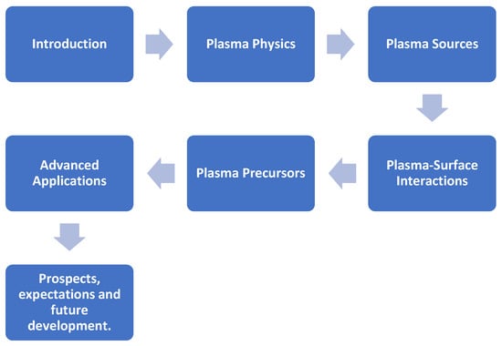
Figure 1.
Flow chart showing section flow adopted for this paper.
2. Plasma Physics
This section provides a foundational overview of plasma physics, with a particular emphasis on concepts relevant to plasma cleaning processes. This section introduces the fundamental principles of partially ionized plasmas, focusing on how their unique properties—including charged particle dynamics and reactive species generation—enable effective surface contamination removal. Key terminology is defined, particularly addressing plasma parameters such as electron temperature, ion density, and Debye shielding, which directly influence cleaning efficiency. Through this underlying theory, the reader will understand subsequent discussions of plasma–surface interactions, contamination breakdown mechanisms, and process optimization in industrial plasma cleaning applications.
2.1. Definition of Plasma
The plasma state is also known as the fourth state of matter and includes ionized gas particles in its makeup. Unlike solids, liquids, or gases, plasma contains free electrons and ions, giving it unique conductive properties. It is commonly found in stars, lightning, and neon signs. Plasma’s high energy and responsiveness to electromagnetic fields make it useful in various technologies, such as plasma cleaning [5]. Plasma consists of ionized gas particles, including negatively charged electrons, positively charged ions, and neutral radicals. These charged particles create a quasi-neutral state, where the overall charge density balances out, maintaining near-neutrality. The proportion of electrons, ions, and neutral species determines the plasma’s properties. This composition influences the plasma’s behaviour and its applications in fields like plasma cleaning [6]. Partially ionized plasmas, the focus of this paper, also contain a significant population of neutral particles.
2.2. Bounded Plasmas Which Are Not Thermally Driven
Plasmas can either be driven by thermal energy (as is the case in stars) or by discharge processes. As an example in the case of many plasma cleaning systems, the plasma is created through energy received via electromagnetic fields. These fields accelerate charge carriers and cause collisions between the particles which collide constantly transferring energy to each other. This energy transfer occurring through the collisions that occur within the plasma can ionize particles as well as break down molecular bonds if the colliding particles have sufficient energy [6]. This will be discussed further in this paper.
It should be explicitly noted that the plasmas employed in cleaning applications are typically confined systems, where the ionized gas is spatially constrained using either physical boundaries (such as vacuum chamber walls) or electromagnetic fields. This confinement serves multiple critical functions, such as maintaining plasma density at optimal levels for surface interactions, preventing unwanted discharge spreading, and enhancing control over the reactive species distribution. The confinement strategy directly impacts key process parameters, including plasma uniformity, radical generation efficiency, and, ultimately, the cleaning effectiveness across treated surfaces. Different confinement approaches ranging from simple geometric configurations to advanced magnetic field arrangements are selected based on specific application requirements, whether for precision semiconductor cleaning or large-scale industrial surface treatment [7]. Confined plasmas present a stratified discharge structure with dark regions on the border of the plasma envelope. These areas are known as the plasma sheath, while the central region, which is the bright area, radiates visible radiation due to the interaction of charged (electrons and ions) and neutral particles. The light emission is due to the collisions that occur between the electrons and the neutral particles. Such collisions cause the particles to reach an excited state. Relaxation from the excited state to the ground state results in light emission.
The central region of the plasma is separated from the walls of the reactor by the sheath regions which are the dark regions at the border zone of the plasma. The sheath regions are dark as the emission of light in these regions is lower than that in the bulk plasma area. The reason for this is that the electron density in the sheath areas is lower than that in the bulk quasi-neutral zone. The quasi-neutral zone, at the core of the plasma, consists of an ensemble of free electrons and positive ions. The charges mathematically cancel each other out and the overall charge of the zone is in equilibrium [5]. The quasi-neutral zone is therefore the region where the electron density (ne) is equal to the ion density (ni), while in the sheath ne is less than ni [7]. The reason for having a lower electron density in the sheath is mostly due to the fact that electrons are 1000 to 10,000 times lighter than ions. This results in the electrons’ ability to escape from the plasma at a much faster speed than the ions into the wall [8,9].
Effectively, the volume bounding the wall surface (inner pre sheath layer) has a very low charge while the outer sheath region has an excessive ionic population. When using DC sources, the sheath region dimensions do not change with time; however, in the case of other sources such as RF systems, the sheath expands and contracts with the radio frequency cycle [7]. The ionization rate in industrial process chambers is normally less than 0.001%, while in the solar core, due to the enhanced temperatures and pressures, it would be close to 100% [10].
2.3. Pressures Used in Plasma Cleaning Processes
Plasma sources used in the cleaning of semiconductor lead frames can be either operate at low pressure (near to vacuum levels) or atmospheric pressure. Vacuum plasmas are more expensive, as they need specialized chambers, including sealing systems and vacuum pumps. However, they are more efficient and effective in the reduction of surface contamination and therefore are the most predominantly used in semiconductor manufacturing [3].
2.4. Plasma Equilibrium
An important classification factor for plasmas is the thermal equilibrium of their constituent particles. Plasmas used in plasma cleaning processes are known as non-equilibrium or non-thermal plasmas. In plasmas confined under low-pressure conditions (approaching vacuum), electrons, energized by sources like microwaves, experience infrequent collisions with other plasma species. This reduced collision frequency leads to inefficient energy transfer from the energetic electrons to heavier species, such as ions. As a result, these plasmas are characterized by an electron temperature (Te) significantly exceeding the ion temperature (Ti), creating a non-equilibrium state [11]. In non-thermal plasmas, the electrons reach higher temperatures than the rest of the plasma constituents at low pressure levels. At pressures of 1 × Pa, the electrons can reach temperatures exceeding 1 × K, while, on the other hand, the gas temperature would be in the region of 1 × K. In thermal plasmas, on the other hand, the pressures would normally be higher, above 1 × Pa, and the temperature of all the plasma components, including ions and electrons, would be close 1 × K [12].
2.5. Ionization
A plasma system can have several different paths toward ionization. The simplest of the paths is the direct ionization path in which a free electron with sufficient kinetic energy, which is greater than the ionization energy collides with a neutral atom, ejecting one of its bound electrons as shown in (1).
This creates a new free electron and a positive ion. Figure 2 below depicts how free electrons collide with atoms (or molecules), knocking an orbital electron out of its orbital. This maintains this ionization process which, in turn, sustains the plasma process [10].

Figure 2.
Schematic diagram representing the ionization process. The orange particles are the electrons which are in the orbitals with the black particles symbolise the free electrons.
This figure illustrates the fundamental ionization process that sustains a plasma. In a plasma environment, free electrons—particles with sufficient kinetic energy—collide with neutral atoms or molecules. During these collisions, if the free electron has enough energy to overcome the atom’s ionization potential, it can eject an electron from one of the atom’s orbitals, thereby ionizing the atom. This ejected electron becomes a new free electron, contributing to the population of charged particles in the plasma.
This process is known as electron impact ionization and is a key mechanism for maintaining the plasma state. Each ionization event produces one positive ion and one additional free electron, which can further collide with other atoms or molecules, continuing the chain reaction. This cascade effect ensures a sustained plasma, as the number of charged particles remains sufficient to support the ionized state.
The ionization process is inherently inelastic because the kinetic energy of the incident electron is partially used to overcome the binding energy of the orbital electron. The newly freed electron and the ionized atom both carry energy away, and the plasma’s overall energy balance depends on continuous input (e.g., from electric fields) to maintain sufficient electron energies for ongoing ionization.
Moreover, the collisions are part of a complex network of collisional and radiative processes within the plasma, including excitation, recombination, and elastic scattering. The balance between ionization and recombination rates determines the plasma density and stability.
In summary, Figure 1 captures the essential electron–atom collision that ejects an orbital electron, generating ions and free electrons. This ionization process is self-sustaining and fundamental to plasma maintenance [13,14].
The reverse process occurs when an ion captures an electron and transitions back from an ionized state to a neutral atom. This is known as radiative recombination when a single electron is captured, releasing the excess energy as a photon. Alternatively, in three-body recombination, the ion captures one electron while a second electron simultaneously absorbs the excess energy to conserve momentum. The latter is a process dominant in high-density plasmas. Both mechanisms restore neutrality, but differ in their energy dissipation pathways.
This ionization process can also occur in what is known as a two-step process (stepwise ionization), where a species which had been previously excited could be ionized by the impact of a second electron. Should a heavy atom hit a particle, this could also cause ionization known as heavy particle impact ionization. This process may be dominant in low-temperature plasmas, such as glow discharges or where heavy-particle kinetics dominate.
Ionization can also occur through the interaction between photons and a neutral atom. In this case, it is called photoionization. The particles forming the plasma can interact with other particles and react with them after colliding. This brings about the creation of charged species and is called associative ionization [15].
2.6. The Role of Negative Ions in Processing Plasmas
In many plasmas used for processing, especially those containing electronegative gases (like oxygen, fluorine, chlorine, SF6, CF4, etc.), negative ions can be formed through processes like dissociative electron attachment outlined in Equation (2) [16].
These heavy, negatively charged species fundamentally alter plasma characteristics compared with purely electropositive discharges. Negative ions contribute to charge neutrality and often lead to a reduced free electron density, which in turn leads to modifications in the electron energy distribution function. Their presence influences the overall plasma chemistry by introducing new reaction pathways, including ion–ion recombination and unique surface interactions if they reach the substrate. While generally confined by sheaths in DC or low-frequency RF systems, negative ions can impact sheath structures and particle fluxes. Understanding their population and kinetics is therefore crucial for controlling radical generation, surface modification, and achieving desired outcomes in plasma cleaning and etching processes [17].
2.7. Collision Cross Section
The collision cross section is an important parameter as it provides the area over which two particles may collide [18]. In the case of an electron colliding with an atom the collision cross section σ may be taken as being the cross section of the atom or πr2, where r is the atom’s radius. This is because the electron’s radius is much smaller than the atom’s. The collision cross section depends on the particular gas, as well as parameters such as the collision type, energy of the electron, and coulomb interactions [12].
The collisions that occur between the particles making up the plasma are inelastic and the kinetic energy is converted into heat. It is crucial to have the proper understanding of the cross section for each collision process in order to be able to set up the proper non-thermal plasma process and create the correct kinetic model of a plasma.
The cross section and the particle’s geometric section can also be different. As an example, if few interactions result in a reaction between the two particles, then the cross section can be taken to be smaller than the geometric section. In a plasma, an elastic collision between two electrons or two neutral particles is in the range between and m2 in the case of thermal electrons or neutral collisions in a weakly ionized plasma. For elastic scattering at high energies, the cross section often decreases due to reduced interaction time [18]. This varies depending on the substance itself; for example, oxygen possesses an electron attachment cross section that is very large.
3. Plasma Sources
Plasma sources are the fundamental means of generating and sustaining the ionized medium required for plasma processing. Their design and operational principles dictate key performance characteristics, such as plasma density, uniformity, and process control. In this paper, five types of plasma sources will be reviewed, namely direct current and pulsed current, radio frequency (RF), microwave, microwave using electron cyclotron resonance (ECR), and dielectric barrier discharge (DBD). Radio frequency and microwave sources are the most common source types used in semiconductor lead frame cleaning industry [3].
3.1. Introduction to the Scoring
These sources will be reviewed in this section and will be scored and contrasted using a specifically set up scoring system that reviews each source individually and then compares the scores in the conclusions. To provide a concise comparative overview of different plasma sources and process gases for semiconductor packaging applications, this review introduces a semi-quantitative scoring system. The scores, ranging from 0 (least favourable/effective) to 10 (most favourable/effective) for each defined parameter, are derived from the comprehensive synthesis and critical assessment of the peer-reviewed literature, which looks at established plasma physics principles and reported industrial practices. This methodology aims to distil complex information into a more accessible format for technical personnel, highlighting key strengths and weaknesses. It is important to note that these scores represent general trends and relative performance; specific application requirements and optimized process parameters can significantly influence outcomes.
The parameters used to score each source are shown and explained in Table 1.

Table 1.
Parametric scoring criteria used for each system.
Scoring Criteria for Plasma Sources (Based on Table 1 Parameters)
For each plasma source, the following parameters (as detailed in Table 1) were evaluated. The scores were assigned based on the preponderance of evidence in the literature as presented in the rubric Table 2.
Table 2.
Parametric scoring criteria used for the comparison of the plasma sources.
3.2. Direct Current and Pulsed Direct Current Plasma Source
Direct current (DC) plasma sources represent the simplest and most fundamental type of plasma generation system. These sources operate by applying a continuous voltage potential between two electrodes in a low-pressure gas environment. This creates a stable glow discharge through electron avalanche ionization. Their straightforward design, consisting essentially of a power supply, anode, and cathode, makes them particularly advantageous for basic plasma studies and industrial applications where process simplicity is prioritized over precise control. However, DC plasmas are typically limited to conductive or semi-conductive target materials, as dielectric surfaces cause charge accumulation that terminates the discharge. Therefore, the setup would consist of two electrodes having an opposite polarity being installed in the plasma chamber in contact with the gas. A high voltage is applied across the electrodes to ionize the gas [6].
In a pulsed direct-current plasma source system, the energy transfer can be managed by controlling the duty cycle. Pulsed direct current (DC) plasma sources offer superior control over energy transfer through precise modulation of the duty cycle. Through the use of pulsed systems, higher charged densities can be achieved with less lead frame damage being caused [6,25]. Table 3 shows the grading parameter scores achieved for DC plasmas sources.
Table 3.
Grading of parameters for direct current plasma source.
3.3. Radio Frequency Plasma Source
RF plasma sources are more dominant in applications using physical bombardment types of reactions. Many of the RF plasmas reviewed operated in strip format, cleaning one strip at a time, and were found to utilize frequencies in the RF range of the electromagnetic spectrum, generally at 13.56 MHz [3]. Two main types of couplings in which RF fields can be applied to the plasma were reviewed, namely capacitive and inductive coupling, as will be described below.
Capacitively coupled plasma (CCP) systems generate plasma by applying radio frequency (RF) power between two parallel electrodes [31]. One electrode is connected to the RF generator while the opposing electrode is grounded, creating an oscillating electric field that sustains the plasma discharge in the inter-electrode region [7]. Typical CCP configurations feature electrode gaps of 1–10 cm and operate at RF power levels between 0.5 and 2 kW, with the exact parameters depending on specific application requirements. The plasma density is around 1 × to 1 × m−3 [7].
In contrast with capacitively coupled plasmas, inductively coupled plasma (ICP) systems generate plasma through an electromagnetic field created by an RF-powered coil positioned outside the plasma chamber, typically separated by a dielectric window. The primary RF source (often 13.56 MHz) drives the coil, inducing a time-varying magnetic field that ionizes the gas and sustains a high-density plasma. Many ICP systems employ a secondary RF bias source connected to the substrate holder, allowing independent control of ion energy while maintaining high plasma density. This dual-source configuration enables the precise tuning of both plasma density (typically 1016–1018 m−3) and ion bombardment energy, making ICP systems superior to single-source CCP devices for applications requiring high-density, low-pressure plasmas with independent control of ion flux and energy [7,31].
The reviewed literature has also identified batch-type RF plasma systems, which have the capacity of handling lead frames in bulk form within magazines. In these cases, the RF generator operates at the same frequency as other RF plasmas, namely 13.56 MHz and a power of up to 1000 W [32]. Table 4 presents the grading parameter scores for RF plasma sources.
Table 4.
Grading of parameters for radio frequency plasma source.
3.4. Microwave (Non-ECR) Plasma Source
Microwaves are one of the common sources used to excite gas molecules. This type of electromagnetic plasma source is more dominantly used for chemical reaction processes, as this plasma type creates more electrons that the radio frequency type and attains a higher cleaning rate predominantly due to the fact that this plasma type operates at higher frequencies than RF plasma systems [3]. Normally, microwave systems operate at a frequency of 2.4 ± 0.5 GHz, which is the industrial microwave frequency, selected especially to ensure that there is no disturbance of communication channels. There are magnetron tube generators, which are specifically built to operate at this particular frequency with high efficiency. Such magnetron tubes consist of a structure that includes an anode, hot filament cathode, magnets, and an antenna. Resonance at the frequency of operation of the magnetron is achieved at the anode. The power generated by the magnetron is then transferred to the antenna.
The microwaves sustain the plasma when the electromagnetic waves manage to impart sufficient energy to the electrons when penetrating into the plasma. Through the combination of electric and magnetic fields, electrons are made to oscillate inside the magnetron and accelerate from the cathode to the anode [36].
The formation of electrons in a microwave plasma source is proportional to the square of the frequency as outlined by Equation (3) [37].
where
- is the maximum electron density;
- f is the source frequency;
- m is the electron mass;
- is the permittivity of free space.
An important parameter in microwave plasma systems is the critical electron density. This is the electron density beyond which the microwaves cannot penetrate the plasma anymore. In the case of a plasma system operating at a frequency of 2.45 GHz, the critical electron density value is 7.6 × . The critical electron density is determined by Equation (4) [37].
where
- is the permittivity of free space;
- is the electron mass;
- q is the electron charge;
- is the angular frequency.
Once the plasma reaches the critical electron density, the microwave electromagnetic waves can no longer propagate and instead become evanescent [38]. A system operating at higher frequency will achieve higher critical density in the plasma, which means that higher levels of power will be absorbed before the incoming microwave power is reflected out by the plasma. The literature includes studies comparing two plasma systems operating at different microwave frequencies, one at 2.45 GHz and the other at 5.8 GHz. It was determined that the absorbed power in the system operating at the higher frequency was nearly twice as high. Higher-density plasmas can be created with lasers operating at optical frequencies or even gamma rays, which generate the highest-density plasmas of all [36]. These two sources are not considered in this field and hence will not be explored further here. It is also important to note that plasma density is not uniform throughout the plasma, with a higher plasma density at the area in which the electromagnetic radiation is incident with a significant reduction in density toward the plasma bulk. By increasing the power, the microwaves can be pushed into the critically dense plasma, thus achieving even higher densities; however, the efficiency of the system is reduced. For this reason, regimes such as Landau damping or electron cyclotron resonance (ECR) are used to achieve anisotropic plasmas with plasma densities that are significantly overcritical [36]. ECR systems will be studied in the next section.
As mentioned earlier, microwave frequencies are significantly higher than radio frequencies; therefore, more electrons are produced in microwave systems. It is also important to note that the higher the source frequency, the higher the kinetic energy of the electrons that are produced [3,39]. In the case of low-frequency systems operating up to 3 MHz, the power can be transferred through cables; however, in this case, since the frequency of operation is in the GHz range, transfer through lines suffers substantial power loss. Therefore, in the case of such high-frequency microwave systems, power transfer is conducted through the use of hollow conductive structures called waveguides, which enables the creation of a high radical density [40].
Microwave plasmas, especially those generated in low-pressure conditions tend to have very low sheath voltages compared with plasmas created by DC or RF sources. This minimizes ion-induced surface damage and makes them well-suited for applications requiring precise and non-destructive cleaning [40]. In a microwave plasma system, the sheath would be around 3 to 14 times the Debye length [41,42,43]. Thus, for a plasma with electrons having an energy of 5 eV and an electron density of , the Debye length would be around 0.2 mm, with a sheath being 0.6 to 2.8 mm thick [36].
On the negative side, it is reported that, although microwave devices have improved in the achievable power levels, such an increase has been coupled with a reduction in microwave pulse length. This pulse shortening means that an increase in power would still see the radiated energy remaining at the same power level [37]. Table 5 presents the parametric grading achieved for microwave (non-ECR) plasma sources.
Table 5.
Grading of parameters for microwave (non-ECR) plasma source.
3.5. Microwave Using Electron Cyclotron Resonance (ECR) Plasma Source
As mentioned above, ECR is a method based on wave resonance which is used to achieve an over critically dense anisotropic plasma. In this case, the anisotropy is produced by the static magnetic field, which is introduced into the plasma chamber to act on the particles in conjunction with the electromagnetic field. This static field allows the microwave power to be absorbed by the electrons through a mechanism that is different to particle collision, hence being denoted as collision less absorption [45]. Microwave radiation along a magnetic field allows the waves to travel into the plasma absorption zone, even in the case of a dense plasma. As mentioned above, when there is a high plasma density, there would be total reflection of the incoming electromagnetic field in a non-ECR plasma system. The static magnetic fields, however, allow the electromagnetic radiation to propagate, even when the plasma density exceed the critical value [18].
In this process, the high-frequency waves travelling through the plasma along the stationary magnetic field interact with the electrons in the plasma. The microwaves have limited interaction with the ions since they are slow moving. The electrons, on the other hand, being very mobile, are trapped and carried forward by the waves. If the velocity of the electrons matches the waves’ phase velocity, the electrons are accelerated.
Field experimentation involving several gases such as hydrogen, helium, argon, and oxygen has shown that the presence of the static magnetic component was crucial in the production of a dense plasma. In the case of such magneto-active plasmas, testing with a 1 kW MW source showed that it was only easy to initiate the plasma when a magnetic field was present at a value of B = , and hence the system was in ECR condition. At this value of static magnetic field, the electrons were therefore forced to gyrate around the magnetic flux lines at the Larmor radius. This circular trajectory radius, also called gyroradius, is determined through the fact that the particle speed multiplied by the magnetic flux density of the field is balanced by the centripetal force [45].
, the value of magnetic induction necessary to achieve ECR, is outlined by Equation (5) [36].
where
- is the 2.π.cyclotron frequency [Hz];
- is the mass of an electron;
- e is the electron charge.
The particles’ velocity remains constant as the magnetic field’s force is perpendicular to the motion at all times. Since the magnetic field cannot change the particle’s kinetic energy, particles with higher energies, having higher velocities, orbit the magnetic field lines at a further distance, but complete the revolution at the same time as particles orbiting at lower orbits due to having lower energies [45].
In a case where the cyclotron frequency f was equal to 2.35 GHz (ω = 14.76 GHz), the value of magnetic field induction was = 8.4 × Tesla or 840 Gauss [36]. For a microwave frequency of 2.45 GHz, which is the one mostly used in industry, resonance occurs at a value of magnetic induction equal to 875 Gauss or 87.5 mT. The static magnetic field can be generated either through permanent magnets or else through electromagnets.
ECR enables the achievement of collision-less plasmas at very low pressures, which can be below 1 Pa, where the ionization degree can reach 100%, thus achieving plasma densities of up to 1 × , even with pressures of 1 mTorr [36]. This is substantially more than what is achieved in plasmas operating at pressures of between 1 and 100 Pa, where the degree of ionization is less than 1%. At lower pressures below 1 Pa, a higher degree of ionization of 10% can be achieved, which is still lower than that achieved by an ECR process [46].
In an ECR system, the pressure must actually be low to reduce the possibility of electron neutral collisions, thereby allowing the electrons to gyrate for a sufficiently long time to obtain sufficient energy to ionize neutral particles [18].
As stated above, most of the energy imparted by the microwaves goes to the electrons, with the ions gaining little. Microwave plasmas are therefore not suitable for processes that are based on surface bombardment, such as ion etching, unless combined with other processes, such as RF or DC-based plasma processes. On the other hand, the process of energizing and hence stripping away of electrons favours the formation of radicals. Such radicals are unstable and therefore very reactive chemically. This can be several orders of magnitude higher than that in reactions involved in conventional equilibrium processes. In such plasmas designed to work chemically, the only relevance for having the electron is the particle activation, as only the heavier ions have the mass and charge state necessary to conduct surface reactions [47,48,49].
Gyrating particles produce a magnetic field, which opposes the external field, thus reducing it. Therefore, plasmas are inherently diamagnetic [45]. Table 6 presents grading of parameters for microwave ECR plasma sources.
Table 6.
Grading of parameters for microwave ECR plasma source.
3.6. Dielectric Barrier Discharge (DBD) Plasma Source
Dielectric barrier discharge (DBD) plasma systems involve electrical discharge between two electrodes separated by an insulating dielectric barrier. It uses high-voltage alternating current, ranging from lower RF to microwave frequencies. The plasma is created through high-voltage pulses and the lead frames are passed through the plasma, which operates continuously. The plasma is created by capacitive coupling, as shown in Figure 3, which presents a schematic of a DBD plasma [13]. The dielectric limits the current flow into the plasma, thus preventing arcing. The discharge is sustained due to the fact that, at atmospheric pressure, frequent collisions may occur due to the high density of gas molecules [55].

Figure 3.
Schematic of DBD plasma. The black areas show the electrodes, whereas the blue areas show the dielectric materials [56].
DBD sources have performance that compares well to that of pulsed DC systems. These systems also allow for operation under atmospheric conditions and can be used for inline plasma systems. However, not all dielectrics can operate with DBD sources [6]. DBD plasmas are used for cleaning applications and surface preparations; however, systems based on DBD mostly operate at atmospheric pressure, which means that they would not require vacuum chambers to operate. Table 7 shows the grading of parameters for DBD plasma sources.
Table 7.
Grading of parameters for dielectric barrier discharge plasma source.
3.7. Dielectric Coplanar Surface Barrier Discharge (DCSBD)
The dielectric coplanar surface barrier discharge (DCSBD) source is a specific type of DBD. The DCSBD is an innovative arrangement designed to produce a large-area, uniform plasma layer that is open to the environment at atmospheric pressure.
The main difference is that, in the case of DCSBD plasma sources, the discharge is generated on the surface of a single dielectric plate. All electrodes, typically in a series of parallel metallic strips or an interdigitated pattern, are on the same plane and are therefore coplanar.
In DCSBD plasmas, all the electrodes, which are typically formed from a series of metal strips having a parallel or an interdigitated pattern, are embedded within or on one side of a single dielectric plate. Similarly as was the case in DBD plasmas, the electrodes in the system are covered by a dielectric material for which the barrier prevents the electrical discharge from turning into a hot, high-current arc, thus limiting the current flow, keeping the plasma stable and cold. The AC voltage is applied between adjacent electrode strips, creating a significant electric field to be formed. This strong electric field at the edges of the electrodes causes gas breakdown on the dielectric surface and forms a plasma, which then spreads laterally over the surface. The plasma forms as a thin, uniform layer on the surface of the dielectric, spreading across the area above the electrodes. Thus, unlike DBD plasmas, in this case, the plasma is not formed in the gap between the electrodes, but rather on top of them.
The key advantage of a DCSBD plasma is that it produces a very uniform, diffuse, and stable plasma layer at atmospheric pressure, especially in air. The plasma is completely open and accessible on one side, which leads to it being used for treating large, flat surfaces that are passed over the plasma body. Figure 4 provides a schematic representation of a DCSBD plasma system. The dark-grey area represents the ceramic base layer, while the light-grey area presents the dielectric layer. Other features include orange and green structures, which represent the electrodes that are alternatively connected to the positive and negative sides of a high voltage generator. The plasma formation is seen as the yellow-shaded zone formed above the dielectric layer [63].
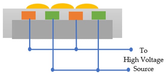
Figure 4.
A schematic view of a DCSBD plasma system.
The reviewed literature has indicated that DCSBD plasmas are mostly used under atmospheric conditions as a fast, cheap, and effective method to simultaneously clean and activate a silicon surface. The oxidation it causes is a key part of the activation process that makes the surface highly useful for subsequent coating steps. While this is desirable in the case of wafers, it would be counterproductive in the case of lead frame cleaning [63].
Table 8 provides the grading of parameters with respect to DCSBD plasma sources.
Table 8.
Grading of parameters for dielectric coplanar surface barrier discharge plasma source.
4. Plasma Interaction with Surfaces
With respect to the handling of lead frames, the literature has indicated the existence of two types of plasma cleaning systems, namely batch-type and strip-type. Batch-type plasma systems are used in cleaning processes involving high volumes. This type of plasma cleaning utilizes slotted magazines in which a number of lead frames are placed. The processing time for this type of plasma is typically longer than that used in strip-type plasmas; however, one must of course keep in mind that many lead frames are being processed at the same time. Batch-type plasma processes typically do not produce the same level of uniformity as can be found in strip plasma, since the lead frames are in different positions within the chamber [3].
Strip-type plasma cleaning systems allow the plasma to be applied directly to the lead frames, which are introduced into the chamber sequentially. The maximum ion concentration is able to reach the surface of the lead frame when this configuration is used. Uniformity of action was also confirmed in the reviewed literature. On the negative side, it must be said that strip plasma systems require significantly more handling of strips and also normally clean one lead frame at a time, thus having low throughput [3].
For both the batch-type and the strip-type plasma, gas flows into the chamber can either be pulsed or continuous.
Pulsed flow allows for a program to be set up where the gas flow of particular gases can be stopped and started during the ongoing plasma cleaning process. In pulsed flow processes, the various gases are introduced separately and sequentially into the chamber. The literature has indicated that introducing the reactive gases over a short period of time, say over 2 s, avoids increased oxidation and surface etching. For reactive gases, the literature indicated that high flow rates can dislodge physical contaminants from the surface of the lead frame. On the other hand, inert gases are introduced at low flow rates over a longer period of time, say 10 s [3].
Continuous-flow processes are those in which gases, inert and reactive, are introduced into the chamber together at a flow rate that is fixed. The reviewed experimental work indicated that a constant flow over a longer time period demonstrated an improvement in wettability and uniformity over pulsed-flow processes [3].
A key difference of DBD plasmas and DC plasma systems compared with other types is the possibility to operate at atmospheric pressures without the need for a vacuum chamber. However, the literature has indicated that plasma systems operating at near-vacuum pressures are preferred over atmospheric plasmas for semiconductor cleaning applications due to several key advantages, one of which is contamination control [67].
Under such conditions of very low gas pressures, there is a reduced presence of airborne contaminants and particulates that could settle on semiconductor surfaces. This means that vacuum plasmas allow for cleaner reactions with fewer unwanted byproducts. The literature has also indicated that vacuum plasmas offer better plasma uniformity since, in a vacuum, the mean free path of plasma species is longer, leading to more uniform and controlled energy distribution, which is critical for precise semiconductor processing. On the other hand, atmospheric plasmas tend to produce filamentary or micro discharges, leading to non-uniform treatment and potential damage. Furthermore, vacuum chamber-based plasmas allows for fine-tuned chemistry, enabling the selective removal of organic residues, oxides, or specific layers without affecting underlying materials, as well as the possibility of conducting effective ion bombardment, where low-pressure plasmas allow for controlled ion energy, thus avoiding excessive surface damage [24].
Another advantage of vacuum plasma systems is the persistence of reactive radicals such as hydrogen, which would have longer lifetimes due to reduced collisions. This also enhances their effectiveness in cleaning processes because, in a vacuum, there would be less gas phase recombination. In a plasma operating at atmospheric pressure, reactive species quickly recombine, thus reducing cleaning efficiency. Vacuum plasmas also have reduced arc formation when compared with atmospheric plasmas, which often suffer from arcing. Such arcing can damage delicate semiconductor structures [68].
In this section, we will review how the species described earlier in this paper interact with the surfaces being cleaned. The interaction of two different states of matter makes the characterization process immeasurably more complex than when one is studying an unbound plasma. When plasma particles collide with the particles on the lead frame’s surface, they can either be reflected or else adsorbed. The latter occurs due to the formation of bonds between the plasma and the surface particles. At the lead frames’ surface, the particles can react and form bonds with atoms found on the surface of the lead frame or other adsorbed particles. The particles can bind two surfaces through one of two regimes, either physisorption or chemisorption.
The bonding regime underlying physisorption is based on the interaction of electrostatic forces, such as dipole–dipole interactions. Physisorption is therefore a surface phenomenon where gas molecules or atoms adhere to a solid or liquid surface due to weak van der Waals forces (or electrostatic interactions) without forming chemical bonds. Chemisorption, in contrast, involves chemical bonds formed by valence electron interactions, such as sharing or transfer. Oxygen and hydrogen are examples of plasma particles that react with the surface in this way. In the case of the latter, the hydrogen molecules break apart upon impact with lead frame surface, with the products being chemisorbed separately [27].
Apart from the chemical aspects, plasmas also interact with surfaces physically through bombardment processes, as will be explained in the next subsection.
4.1. Physical Bombardment of Surface
Physical bombardment or ablation describes the mechanism underlying the removal of surface layers through mechanical kinetic bombardment. Such bombardment is conducted through the use of electrons and especially heavy ions, which are used to dislodge particles from the surface through kinetic interaction [69]. This is also known as “Physical Plasma”, where the plasma interaction occurs through physical interactions, rather than chemical reactions. Interaction with targets occurs through inelastic collisions brought about by the acceleration of argon toward the target through electric fields [70].
Through this physical process, plasmas can also be used to deposit layers on surfaces, thus altering the physical or chemical properties of the surface itself. The radicals that are used must therefore be selected well to ensure that such does not occur in lead frame plasma cleaning systems [69,71].
4.2. Chemical Reactions with Surfaces
As discussed in the introduction to this section, chemical reactions between a plasma and a surface can either result in the plasma species moving into the surface or particles from the surface leaving into the plasma [69].
Plasmas induce chemical reactions on surfaces through interactions with reactive species such as radicals, excited molecules, and ions. These species drive oxidation, reduction, or other surface chemistry processes without relying on physical bombardment. For example, oxygen plasmas generate reactive oxygen species, such as O, , and , that react with organic contaminants, breaking them down into volatile by products like CO2 and , which are easily removed [23]. Similarly, hydrogen plasmas facilitate the reduction of oxides or the removal of surface hydrocarbons by forming volatile compounds, such as or . The chemical selectivity of plasma–surface interactions depends on the gas composition, energy levels of the reactive species, and the nature of the lead frame, allowing precise control over surface cleaning, functionalization, and modification processes [14].
These chemical reactions occur primarily through the adsorption and reaction of reactive species generated within the plasma phase. Atomic radicals, such as O, H, and Cl, metastable molecules, and molecular fragments diffuse into the surface and participate in heterogeneous reactions dictated by thermodynamic and kinetic constraints. For instance, in oxygen plasma cleaning, atomic oxygen (O) oxidizes hydrocarbons, to form volatile CO, CO2, and H2O. The reaction rate depends on factors such as the surface energy, temperature, and residence time of the species [14,72].
Plasma-induced surface chemistry is further influenced by secondary reactions, such as radical recombination and competitive adsorption, which impact the efficiency of material removal or functionalization. By tailoring process parameters such as pressure, gas composition, and power input, plasma systems can be optimized to achieve highly selective and controlled chemical surface modifications [73].
The next section will review the particular characteristics of each of the gases, which can potentially be used in plasma cleaning processes.
5. Plasma Precursors
With regard to plasma precursors, the literature has shown that plasma systems outlined in the previous sections can work with a wide range of substances. The plasma precursor is an important and crucial parameter in achieving optimal plasma characteristics and ideal wettability results. To accurately model plasma physics and chemistry, extensive data are required and sources such as the LXCat project are sources of online data, which are crucial for modelling low-temperature non-equilibrium plasmas [74]. This section will examine precursors that are used to produce and will seek to establish their acceptability for use in semiconductor lead frame cleaning. The substances are being compared at the same plasma conditions, i.e., each of the substances is at the same concentration and has the same external plasma parameters. Table 9 presents the parametric scoring criteria used for the plasma precursors. These criteria will be used to conduct the comparative parametric assessment.
Table 9.
Parametric scoring criteria used for the comparison of the plasma precursors.
5.1. Hydrogen
Hydrogen plasmas are used for the removal of surface oxide layers on many types of surface finishing, including gold plating. The literature has presented studies that were conducted on NiPdAu-plated lead frames treated with an oxygen plasma. These formed a Au2O3 layer after the oxygen plasma process. Subsequently, the lead frames were subjected to a hydrogen plasma process in a batch microwave plasma system, thereby removing the oxide layer [3]. Studies on similar NiPdAu lead frames have shown that the recontamination rate is reduced through the use of hydrogen. This reduction in the recontamination rate was observed to be up to 50% [75]. One may say that hydrogen has a unique ability to remove many types of contaminants from copper–lead frames, including the halogens, hydroxides, and oxides of copper. The equations for some of these reduction processes in copper lead frames can be seen in (6)–(8) [76,77].
Cu2O + 2H → Cu2 + H2O
CuO + 2H → Cu + H2O
Cu(OH)2 + 2H → Cu + 2H2 O
Apart from removing the oxide layer, hydrogen saturates immobilized radicals, thereby providing a protective layer on metals. Such a protective layer prevents surface oxidation over an extended time period [78].
Hydrogen’s plasma chemistry is quite complex to model and can be approximated by around 26 volume reactions and 6 surface reactions. There are many species involved, such as electrons, molecular hydrogen , neutral hydrogen atoms (H), protons (, hydrogen anions (, molecular hydrogen ions (, trihydrogen cations (, and three vibrationally exited states, (v = 1), (v = 2), and (v = 3). Apart from this, there are also four electronically excited states [79,80,81,82,83].
The ion which is the most abundant in hydrogen plasmas having a degree of dissociation less than 50% is the ion [36]. ions are actually the most prevalent ion in hydrogen glow discharge processes and therefore are an important factor in hydrogen-based plasma processes [84]. This can change depending on the specific conditions underpinning the particular plasma process [85].
The main processes underpinning the plasma process will now be explained in the context of hydrogen [86]. These processes hold true for other elemental and molecular plasmas, as will be explained in the other subsections tackling the other substances.
5.1.1. Elastic and Inelastic Collisions
Collisions, both elastic and inelastic, between the particles forming the plasma are the main pathway of energy transfer between electrons, ions, and neutral particles. In the case being studied by this paper, namely non-equilibrium low-pressure plasmas, collisions are normally binary collisions. The result of a collision between two particles is a function of the particles’ energy, mass, charge, and the particles’ cross sections.
Therefore, inelastic collisions represent any interaction resulting in a net change in the system’s kinetic energy due to its conversion into internal excitation, potential energy associated with ionization or dissociation, or the emission of radiation [27].
5.1.2. Vibrational Excitation
Vibrational excitation is an important process in the plasma physics of non-equilibrium plasmas involving molecular gases such as hydrogen. H2 is capable of maintaining vibrational energy for an extensive period and can use such energy in ensuing chemical reactions. The lifetime of vibrationally excited molecules is in the region of to s, which is long when compared with chemical reaction time periods and the exchange of vibrational energy. This excitation method is a dominant form of energy transfer in the case of molecular hydrogen. Most of the discharge energy, which can be up to 95% in some cases, can be vibrational excitation produced through the impact of electrons. One of the reasons for this effectiveness is because the energy level for vibrational excitation is low when compared with the energy levels involved in other plasma reactions [18]. The three reactions involving vibrational excitation for hydrogen have threshold voltage levels ( of 0.52 eV, 1.0 eV, and 1.5 eV, and the reaction is denoted by (9) [87].
where
- = (v = 1), (v = 2) or (v = 3).
The vibration excitation process of hydrogen presented in (9) usually results in the formation of an intermediate having a short lifetime. The reason for this is that vibrational excitation is not usually the result of a direct elastic impact between an electron and the hydrogen molecule itself, but an ongoing resonant process. A direct consequence of this is that vibrational excitation cross sections can be much larger than one would expect from electron to molecular collisions, given the extreme size disparity between the two particles. The maximum cross section for the vibrational excitation of by electron impact is 4 × [87].
5.1.3. Electronic Excitation
This process occurs with excitation energies that do not significantly exceed ionization potential; however, the energy levels involved are much higher than those involved in vibrational excitation. The key difference between electronic excitation and vibrational excitation is that, while the latter involves changes in the vibrational state of H2, electronic excitation involves changes in the electronic state of the molecule. Therefore, in the case of vibrational excitation, the bonds between atoms vibrate more intensely, but the electrons stay at the same energy level. On the other hand, in the case of electronic excitation, an electron jumps to a higher energy orbital, changing the molecule’s electronic state.
The four states for electronic excitation related to hydrogen have energy levels of 8.9 eV, 11.37 eV, 11.75 eV, and 12.4 eV [87]. The radiative lifetime of electronically excited particles is times shorter than the lifetime of vibrational excited ones, which could mean that this excitation mode could be less conducive to surface chemical reactions than the vibrational excitation mode [18]. However, it is also important to note that electronic excitation is a precursor to ionization, which is a fundamental process in the maintenance of the plasma state [88].
5.1.4. Dissociative Excitation
The reaction for dissociative excitation is shown by Equation (10) and has a threshold energy of 16.6 eV [87,89].
As can be seen in (10) the dissociative excitation process involves the collision of an electron with a molecule with sufficient force to cause it to dissociate while simultaneously exciting one or more of the resulting fragments, imparting in them substantial kinetic energy. indicates a hydrogen atom that is left in an excited state (), typically with principal quantum number n = 3. This radiates visible light emission in the Balmer series [90,91,92].
5.1.5. Ionization
This category includes the reactions that are cases where a direct electron impact results in the ionization of the whole hydrogen molecule or its fragments. This reaction occurs when the ionization potential is not significantly exceeded by the electron energy [18]. The reaction shown by Equation (11) outlines the ionization of the hydrogen molecule at a threshold voltage of 15.4 eV, whereas (12) presents the ionization of H with of 13.6 eV [87].
5.1.6. Dissociative Ionization
Dissociative ionization takes place at high electron energy levels that exceed the ionization potential [18]. In this fragmentation process, ionized product particles are produced. Hydrogen ions can undergo dissociative ionization too, with the process having a lower energy threshold than that occurring with neutral due to the fact that the species would be pre-ionized. Some examples of dissociative ionization reactions for a low-temperature hydrogen plasma are being presented in Equations (13)–(15) [87].
The threshold voltages for the three reactions are 34.8 eV for Equation (13), 4 eV for Equation (14), and 19.4 eV for Equation (15). One can appreciate the difference in threshold voltages between the dissociative ionization of the neutral and ionic forms of the hydrogen molecule [87].
5.1.7. Recombination
The recombination process for electrons and ions is a very exothermic process, with the energy released depending on the particle’s ionization potential. Three types of recombination will be discussed here, namely dissociative, three-body, and radiative electron–ion recombination.
In the case of molecular gases, the dissociative electron–ion recombination process is the fastest mechanism of electron neutralization. This process follows the mechanism presented in (16) [18].
As can be seen by Equation (16), the dissociative recombination process starts with an electron being trapped by a molecular ion. The maintenance of the state of auto-ionization leads to more stable products being produced. The rate of reaction for diatomic and triatomic ions, as is the case for hydrogen, exhibits reaction rate coefficients around the mark [19].
The dissociative recombination equations in the case of hydrogen plasma are shown in (17) and (18). The threshold voltage levels for Equations (17) and (18) is 0.01 eV [87].
Three-body recombination, also known as ternary association, is a termolecular reaction where three particles collide, resulting in the formation of a bound state between two of the particles, while the third particle escapes freely. In plasma cleaning systems, three-body recombination plays a crucial role in maintaining the efficiency and effectiveness of the cleaning process.
In the context of plasma cleaning, three-body recombination helps to neutralize charged particles, reducing the overall plasma density and preventing potential damage to the surface being cleaned. This process ensures that the plasma remains stable and effective in breaking down contaminants into volatile compounds, which are then evacuated from the chamber. However, three-body recombination can reduce the overall ionization level in the plasma, affecting the efficiency of cleaning by decreasing the number of reactive species available for surface interactions. To mitigate this, plasma cleaning systems are often designed to operate at lower pressures, minimizing three-body collisions and sustaining a higher density of ionized particles for effective contaminant removal [93].
The three-body recombination competes with dissociative recombination at high electron concentrations exceeding . At a 1 eV electron temperature, three-body recombination only in case of electron densities being exorbitantly high exceeding . The excessive energy in this case is transferred to the third body, the electron [18].
The third process of recombination, radiative electron–ion recombination, is an electron–ion process that is slow compared with the other processes, the reason being that a photon needs to be emitted during the interaction of an electron and an ion [18]. The process shown in Equation (19).
where
e + A+ → A + ħω
- e represents a free electron;
- represents a positive ion;
- A represents the resulting neutral atom or molecule;
- ħ is the reduced Planck constant;
- ω is the angular frequency of the emitted photon.
It is important to note that this process has a low cross section of and is only a key player if molecular ions are present and mechanisms such as three-body recombination are suppressed. This mechanism is therefore not very relevant in the case of hydrogen plasmas [18].
5.1.8. Surface Neutralization
In addition to volume processes like three-body recombination occurring within the plasma itself, significant interactions involve surfaces such as the reactor wall or the lead frame. Surface neutralization, potentially detailed in Equation (20), describes this process occurring on the lead frame surface. This is a highly efficient mechanism initiated when an ion captures an electron from the surface material, often forming a highly excited atom [6,94]. The work function (Φ) of typical materials is between 4 and 6 eV. Crucially, the ion’s potential energy (ionization potential, IP, often >15 eV for common ions) greatly exceeds the work function (IP >> Φ). This large potential energy difference ensures that neutralization is highly probable upon contact with the lead frame surface. The combined energy released primarily causes surface heating and may also induce secondary electron emission [27].
where
- S represents the surface material;
- A+ is the ion species in the plasma;
- is an excited molecule or atom.
In this case, the surface takes up some of the energy from the plasma [95]. When the excited electron goes back to its unexcited state, photons are emitted, with each substance emitting photons at different frequencies, thereby resulting in the different colours of the plasmas [10].
The rate of reaction for the surface process is regulated by the adsorption and desorption processes. The adsorption reaction, which is exothermic, is presented as Equation (21) [6].
The adsorption process can be either due to the Van der Waals forces between molecules and the surface or else due to bonding between the plasma particles and the surface. The latter, known as chemisorption, is more exothermic [6].
An important parameter in overall surface interactions, especially those involving adsorption and subsequent reactions like recombination, in the surface neutralization discussion is the sticking coefficient (γ), as presented in Table 10. Coefficient γ indicates the probability of ions and atoms recombining when they touch the walls of the reactor.
Table 10.
Sticking coefficient expressions [96].
This shows that ions hitting the surface are very efficiently converted into neutral hydrogen atoms at the surface, effectively delivering the necessary reactant for the chemical reduction of the copper oxides. A by-product of the reaction is water vapor. If such water condenses on the cold lead frames, it may prove an impediment to further reaction unless removed.
5.1.9. Dissociative Attachment
In , the dissociative attachment process is outlined by Equation (22) [17].
In purely electropositive plasmas, like hydrogen at pressures less than 0.1 Pa (where H− is less dominant) or pure argon, negative ions have a limited impact. However, this process becomes especially important for plasmas using electronegative gases, such as oxygen and the halogens, because the presence of negative ions in these systems significantly alters plasma properties [17].
5.1.10. Heavy Particle Interaction
The ions and neutral particles that make up the plasma also interact with one another and impacts between the heavy particles also occur. However, even if they have similar kinetic energies to the electrons, the chances for ionization are very remote as the velocity of the heavy particles is much lower than that for electrons [18]. Proton transfer is the main mechanism used to produce trihydrogen cations . The process in which ions interact with neutral hydrogen molecules, thereby resulting in a proton transfer between the two heavy particles, is shown in Equation (23) [87,97].
5.1.11. Comparative Analysis
For hydrogen and each of the plasma precursors, the parameters were evaluated based on the literature regarding its plasma chemistry and interaction with typical lead frame materials and contaminants.
To summarize the characteristics outlined in this section, Table 11 presents a grading of the parameters relevant to hydrogen plasmas, outlining their suitability for use in cleaning applications.
Table 11.
Grading of parameters for hydrogen plasmas.
5.2. Oxygen
Oxygen produces a plasma that reacts with contaminants such as organic modules to form oxides such as and . On the negative side, oxygen plasma does promote the metal oxidation of the lead frame surface [3]. Similarly to what has been explained for hydrogen, these reactions involve dissociation, excitation, and ionization, with the most important reactions being presented in Equations (24)–(29). The excitation energies involved going up to 20 eV for the dissociative ionization of oxygen presented in (24) [103].
The most reactive species is , followed by . Both are more reactive than excited oxygen species, followed by atomic and molecular oxygen, respectively [14]. Oxygen interacts with organic substances on the lead frames’ surfaces. The by-products produced during an oxygen plasma process are and H2O. An example of an oxidative breakdown reaction brought about through the oxygen–plasma interaction is shown in (30). Similarly, as discussed for hydrogen, the by-products need to be removed to ensure a constant reaction rate with high efficiency.
Table 12 presents the grading of the parameters relevant to oxygen plasmas to outline oxygen’s suitability for use in cleaning plasmas.
Table 12.
Grading of parameters for oxygen plasmas.
5.3. Argon
Argon is a noble gas with atomic mass of 39.948 u, is inert, and can be ionized into Ar+ ions, which are characterized by energetic nature, albeit not exhibiting a high temperature. When in the plasma state, argon does not react strongly with matter on the surface being cleaned and therefore does not chemically alter surface properties, nor does it react or alter the underlying layers on the lead frames. Of course, ions gain significant kinetic energy when accelerated by the sheath potential toward the surface, making them ideal for use in bombardment processes [70].
The literature has indicated that argon plasma is effective in the micro-roughening of the substrate’s surface. The reviewed experimental work started with the oxidization of copper lead frames at 175 °C for 1 h, after which they were then plasma-cleaned with a DC plasma having a 200 V bias [108]. Surface micrographs of a copper lead frame surface before and after plasma argon bombardment clearly showed the ablative nature of the plasma. The experimental process showed that cleaning in argon for a period of 2.5 min produced a fourfold increase in the strength of adhesion [108].
This was attributed to the thinning of the surface oxide, where the literature indicated that the adhesion of moulding compounds to the lead frame is enhanced when the oxide is not thicker than 25 nm. A rapid decrease in adhesion was observed when the oxide thickness varied between 25 and 60 nm [109].
Argon plasmas also impart two further advantages. They act uniformly over the surface being cleaned and show consistency, even on devices having geometries that have difficult-to-reach areas and are effective to remove organic residues on lead frames. Argon plasmas are also non-toxic, and the plasma cleaning does not produce by-products that are harmful to health or the environment [70].
Argon has a first ionization potential of 15.76 eV.
Table 13 presents the grading of the parameters relevant to argon plasmas to outline argon’s suitability for use in cleaning plasmas.
Table 13.
Grading of parameters for argon plasmas.
Summarizing the benefits, argon plasma treatment is particularly effective for bare copper lead frames. Evidence suggests that the induced surface roughening significantly improves adhesion, leading to enhanced reliability, as demonstrated by the absence of delamination after extensive thermal cycling (one thousand cycles reported) [111,112].
5.4. Helium
Helium is another noble gas that is used in plasma cleaning processes [1]. Helium atoms, having an atomic mass of 4 u, are lighter than argon atoms. It is important to note that mass is an essential characteristic for physical plasmas, since the kinetic energy of particles is dependent on the mass and the square of their velocity. Helium ions therefore do not have a very effective etching efficiency [113].
The first ionization potential of helium is the highest known, at 24.59 eV. This means that it needs a very high energy level to lose one electron compared with other particles, such as argon or hydrogen presented above [36].
Table 14 presents the grading of the parameters relevant to helium plasmas to outline helium’s suitability for use in cleaning plasmas.
Table 14.
Grading of parameters for helium plasmas.
5.5. Other Noble Gases
Like argon, other noble gases are chemically inert, making them primarily suitable for purely physical plasma cleaning processes where chemical reactions are not desired. While xenon and krypton can be used, they are significantly more expensive than argon or helium; xenon, in particular, also suffers from limited availability [113].
Recombination mechanisms, which neutralize charged species, play an important role in plasma decay. The rate of recombination increases drastically as atoms grow larger and possess more electron shells. For example, the recombination rate of helium is approximately 100 times lower than those of krypton and xenon [19].
Regarding neon, stable plasmas have been observed, such as those generated at pressures of 100 Torr in microwave discharge systems [115]. Neon is also commonly used in lighting (neon tubes) and other glow discharge systems [113]. However, despite its availability and ability to form plasmas, no evidence of neon being utilized in plasma cleaning processes was identified in the reviewed literature.
Table 15 presents the grading of the parameters relevant to noble gas plasmas to outline noble gases’ suitability for use in cleaning plasmas.
Table 15.
Grading of parameters for other noble gas plasmas.
Neon could potentially be used for physical plasma cleaning, but argon is significantly more effective (due to higher mass leading to better sputtering) and cheaper. There is no compelling technical or economic advantage to using neon over argon for the standard physical plasma cleaning applications where noble gases are employed. Krypton or xenon might be chosen for specific, niche applications where the absolute highest bombardment is critical, the added cost is acceptable, and potential lead frame damage is managed or tolerated.
5.6. Nitrogen
Similar to oxygen plasma, nitrogen plasma generates reactive species that convert organic contaminants into smaller, volatile molecules. However, unlike oxygen plasma, nitrogen plasma does not significantly promote the oxidation of materials such as copper or silver. This makes nitrogen plasma particularly suitable for cleaning lead frames with these surfaces. Furthermore, nitrogen plasma cleaning is effective against contaminants that are resistant to both oxidation and reduction processes [70]. A higher activation energy is required for nitrogen plasma compared with oxygen plasma, primarily because the strong triple bond in the diatomic nitrogen molecule (N≡N) requires more energy to dissociate [78].
Table 16 presents the grading of the parameters relevant to nitrogen plasmas to outline nitrogen’s suitability for use in cleaning plasmas.
Table 16.
Grading of parameters for nitrogen plasmas.
Nitrogen plasmas have also been used to improve the hydrophilicity of surfaces [118].
5.7. Fluorine and Fluorine Compounds
Gases such as SF6 and CF4 can be used to produce fluorine plasmas, as shown in (31) [27].
These precursors are relatively harmless compounds that allow the safe use of fluorine in lieu of dangerous fluorine compounds, such as HF or elemental halogen [93]. Fluorine plasmas are highly reactive and will readily etch group 14 elements, such as silicon, since fluorine forms volatile fluorides with these elements [119]. No evidence of the use of fluorine plasmas for lead frame cleaning was detected in the literature, probably due to the fact that this most aggressive of species will readily etch the silicon dies, producing SiF, , , and . which are volatile [27]. However, one might consider the use of fluorine for lead frames that do not yet contain dies if any cleaning is needed at that stage as fluorine is used in cleaning applications, such as the cleaning of process chambers. However, the use of such an aggressive element needs to be carefully weighed, as even the equipment needs to be specifically designed, including features such as the use of a remote plasma source to reduce the presence of ions within the process chamber itself [120].
Table 17 presents the grading of the parameters relevant to fluorine plasmas to outline fluorine’s suitability for use in cleaning plasmas.
Table 17.
Grading of parameters for fluorine plasmas.
Due to the reasons mentioned above, especially the high risk of damaging the silicon die and the safety/environmental concerns associated with HF generation, fluorine plasma is generally avoided for lead frame cleaning in standard semiconductor packaging processes.
5.8. Other Halogens—Chlorine and Bromine
Similar to fluorine, chlorine is a halogen and is also highly reactive. Chlorine is useful for removing organic residues, which are more stubborn and challenging to remove. Due to its reactivity, chlorine plasmas are very corrosive and therefore used only when etching is required and when chlorine is specifically needed to remove the material. It must also be kept in mind that the exhaust gases from a chlorine plasma process cannot be exhausted into the atmosphere, but need to be adequately treated [70].
Chlorine and bromine react with silicon and etch it in a way that is crystallographic in nature. While chlorine and bromine do not react with , the reaction of Cl− ions with n-doped silicon is a very fast reaction [8]. Bromine is a less reactive element than the other halogens, fluorine and chlorine [93].
The use of these aggressive halogenic plasmas will therefore not be reviewed further since the scope of this paper is the review of technologies that can be utilized for pre-mold plasmas.
Table 18 presents the grading of the parameters relevant to chlorine and bromine plasmas to outline their suitability for use in cleaning plasmas.
Table 18.
Grading of parameters for chlorine and bromine plasmas.
While Cl and Br are reactive, they are generally unsuitable for cleaning organic contaminants from surfaces like lead frames. They aggressively attack the underlying metal lead frame and form persistent (non-volatile) metal halide residues. Halogens produce hazardous by-products, like HCl/HBr.
5.9. Water
Water vapor can also be utilized as a process gas to produce oxygen and hydroxyl species [125]. Water-based plasmas are more complex than plasmas using monoatomic elementary gases. The energetic electrons impact the molecules and start by ripping away one of the hydrogen atoms by breaking the OH-H bond. The dissociation energy of the OH-H bond is 4.85 eV, which is provided by the collision of the molecule with the energetic electron, as shown by Equation (32). Equations (32) and (34) present the results of other high energy collision processes in the aqueous plasma [126,127].
where
- denotes a high-energy electron.
The charged radicals thus formed are highly reactive and ready to react with other matter to produce new species. The OH radical is the most active oxidation component. It can react with electrode materials and form new species with them. Thus, plasma equipment design needs to factor in ways of avoiding sputtering the surface being cleaned with the material forming the electrode [6]. The problem is further exacerbated due to the fact that water condensation on the cool electrodes can cause an arc path to form, thus speeding up the electrode breakdown mechanism. Thus, the electrode must be specifically designed to avoid this through spacing steam preheating, heating of gas lines, and thermal regulation of the electrodes themselves [128,129].
The quantity of studies discussing based plasmas was not copious, although water vapor plasmas have seen growing interest, particularly in fields like sterilization, surface activation for biomaterials, and some specialized cleaning/etching processes. However, the research effort being carried out in the semiconductor manufacturing field has increased in recent years, and even production-grade equipment was identified. plasmas have high chemical reactivity and enthalpy.
Table 19 presents the grading of the parameters relevant to oxygen plasmas to outline oxygen’s suitability for use in cleaning plasmas.
Table 19.
Grading of parameters for water plasmas.
As discussed, water vapor plasmas contain strong oxidizing species, such as OH and O, and so need to be used judiciously, since these create an oxide layer, rather than remove it. They therefore need to be coupled to other gases for oxide layer production to be reduced. One such example using water plasma successfully reduced the oxide layer production on the copper surface. Tests conducted on copper surfaces showed that an oxygen-based plasma treatment produced a 79.2 nm thick oxide layer, while a comparable treatment with a water-based plasma produced a 1.6 nm thick layer, which could be removed through argon bombardment in thirty seconds. On the other hand, the 79.2 nm thick layer produced by the oxygen plasma took seven minutes to be removed by subsequent argon bombardment [125].
5.10. Ammonia—NH3
The reviewed literature indicated that NH3 plasmas can be used to create both hydrogen and nitrogen radicals, which can be used to carry out a combined cleaning approach utilizing two plasma gases with different characteristics. Ammonia in a plasma can produce a multitude of species including ions such as A number of vibrational excited and electronically excited states are also created [132].
The literature indicated that ammonia-based plasmas were used to achieve oxide removal, surface roughening characteristics, which can be achieved through the hydrogen component, as well as the passivation layer, which can be achieved through the nitrogen component of the plasma. Through this combination, NH3 plasma treatment maintained higher uniformity, higher overall surface conditions, and a smooth reduction process [117]. While published studies on ammonia plasma cleaning of lead frames remain scarce, research efforts have instead focused on its applications in advanced packaging technologies, particularly for 3D stacked semiconductor architectures employing copper interconnects in chip-scale packaging. Such plasma systems were found to utilize an RF source to drive the process [133].
Table 20 presents the grading of the parameters relevant to ammonia-based plasmas to outline ammonia’s suitability for use in cleaning plasmas.
Table 20.
Grading of parameters for ammonia plasmas.
The data outlined above indicate that, while ammonia plasmas presented positive results in certain areas, there are other aspects that need to be researched further. Another area that needs to be studied experimentally concerns findings outlined in the literature presenting experimental work benchmarking the plasma process with a hydrogen plasma. These findings indicated that the former showed less efficacy in the reduction of an oxide layer from a copper lead frame [139]. Therefore, further extensive experimental work would be warranted on the use of ammonia for plasma cleaning processes.
6. Application of Plasma Treatment in Advanced and Emerging Packages
The relentless drive for miniaturization, increased functionality, and improved performance in electronic devices has led to the development of advanced and emerging semiconductor packaging technologies. While these new packaging paradigms present unique challenges in terms of materials, interconnect density, and manufacturing processes, their processing is still highly dependent on the principles of plasma processing outlined in this paper.
A group of advanced packaging relies on stacking and interconnecting multiple dies, often with very fine features and complex architectures. This necessitates extremely clean surfaces and precise surface modification to achieve reliable electrical connections and mechanical integrity. Similarly to the situation with lead-frame-based semiconductor system, cleaning methods, such as wet chemical cleaning, fall short of the requirements needed for such packaging manufacturing; therefore, plasma cleaning needs to be used.
6.1. Flip–Chip Packaging
Flip–chip technology involves attaching a die to a substrate by flipping it upside down and connecting it through solder bumps. Plasma cleaning of copper pillar bumps and under-bump metallization (UBM) are crucial for removing oxides and contaminants that can hinder solderability and lead to joint failures. Plasma treatment also enhances the adhesion of underfill materials, which improves the mechanical reliability of the package.
Regarding the improvement in solderability, the reviewed literature presented the use of hydrogen plasma to clean the bumps, instead of flux in a process known as fluxless soldering. An RF capacitively coupled plasma, the technology of which was outlined earlier in this paper, was used to generate hydrogen radicals that removed the oxide layers, thereby cleaning the bumps instead of flux. This process provides a 48-hour time window in which to carry out the flip–chip connects after the plasma treatment has been conducted [140]. Other papers presented similar work using hydrogen plasmas to remove oxide layers through reduction [141,142].
With respect to the improvement of the underfill process, various papers were reviewed. The reviewed literature showed that gas mixtures of argon and oxygen in a 6:1 ratio were used to produce the plasma necessary to reduce void formation in the underfill. Plasma treatment increased the amount of hydrophilic carbonyl functional groups (O-C=O) on the solder mask surface, which improved underfill wetting. The reviewed paper also underlined that increasing the staging time increased the percentage of unit failures due to void formation [143].
Under-chip plasma cleaning was also found to be used in the improving of the moisture sensitivity level (MSL) performance for flip–chip packaging, thereby enhancing adhesion between silicon nitride (SiN) passivation and underfill, a critical interface prone to failure in MSL tests. In this case, an RF plasma system operating at 300 W was utilized with oxygen and a proprietary unnamed gas being used to produce the plasma. Pure oxygen plasma, when used alone, presented lower contact angles than when the plasma was used with the proprietary gas. However, an improvement in adhesion was noted with the addition of the proprietary gas [144].
The literature comparing the suitability of ,, and Ar plasmas for surface activation beneath flip chips used atomic force microscopy (AFM) to analyse surface roughness and topography after treatment with plasma. The conclusions indicated that Ar plasma treatment caused an imbalance in roughness between the corner and central regions of the substrate and die. plasma treatment, on the other hand, tended to smoothen the surfaces, while plasma treatment increased surface roughness and the surface area difference percentage. The final conclusion was that plasma treatment resulted in the highest surface energy and was therefore the most suitable for improving underfill adhesion and flow in flip–chip packaging due to its effectiveness in activating the surface [145].
6.2. Through-Silicon Vias (TSVs)
TSVs are vertical interconnects that pass through a silicon die, enabling 3D stacking of chips. This technology is an alternative to other bonding techniques, such as wire bonding or flip–chip technologies. TSVs are used to create high interconnection and device density. The literature has shown evidence of plasma being used for various roles, such as the removal of the fluoropolymer and the photoresist residues. This type of bulk material removal is beyond the scope of this paper, since the focus is on cleaning. However, plasmas are also used for the cleaning of the inner surfaces of the TSVs to ensure good adhesion and electrical contact with subsequent layers.
For cleaning the inner surfaces of TSVs, the reviewed literature indicates that three main types of plasma gases are typically used. Oxygen plasma primarily removes organic contaminants (such as polymer or photoresist residues) through chemical reactions. Argon plasma, working via physical sputtering, is used to remove both organic and inorganic contaminants, including thin native oxides. Hydrogen, on the other hand, chemically reduces and removes metal oxide contaminants and can also address some organic contamination. The use of gas mixtures incorporating these gases is also frequently reported in the literature [146,147].
6.3. Wafer-Level Packaging (WLP)
There are two main types of WLP, namely fan-out wafer-level packaging (FOWLP), where the die is embedded in a moulding compound and the interconnects are fanned out over the compound, and fan-In WLP (FI-WLP), where all the external connections (solder balls) are located directly on the wafer surface within the perimeter of the die. In this case, plasma cleaning is required to address various challenges, such as the cleaning of bond pads and modifying surfaces to improve the adhesion of the underfill and encapsulants [148].
The reviewed literature indicated that a mixture of Ar and was selected over other gases, such as , , , Ar, , He, and . This mixture was shown to effectively remove oxide layers. Of course, other plasma gases, such as , are used for the cleaning of photoresist residues (scum) after the photolithographic processes [149]. Other plasma processes involved in WLP are used for the stripping of bulk photoresist after the etching process and dielectric patterning [70].
These processes are beyond the focus of this paper. It was also noted, however, that no single gas mixture can be considered ideal for all applications. A specific recipe must be developed for each application to ensure that it provides the optimal balance for the desired outcome, such as prioritizing adhesion enhancement versus oxide removal [150].
6.4. 2.5D Interposer-Based Packages
2.5D packaging employs an interposer, a substrate acting as an intermediary between the die and the printed circuit board. In this configuration, multiple dies are typically placed side-by-side on the interposer (which may contain TSVs), connecting laterally through it, rather than being directly stacked vertically via TSVs passing through the active dies. A key advantage of this approach is reduced heat buildup compared with dense 3D stacks. During assembly, plasma cleaning plays a crucial role. Specifically, achieving high surface wettability on the interposer is critical for uniform underfill flow between the die and interposer. The literature reports the common use of oxygen plasmas for this purpose, effectively treating the surface to enhance wettability, which consequently allows for the underfill to flow more easily and fill gaps completely [147].
Another reviewed paper indicated that the primary goal of plasma surface treatment in such packages was to improve process performance (including underfill filling time, void reduction, and flow characteristics) and enhance the interfacial adhesion strength of the underfill, specifically on polyimide (PI)-coated RDL interposers. The aim of the plasma process was therefore to improve both processability and reliability. The gas used to produce the plasma was oxygen and the plasma treatment significantly increased surface wettability, making it more hydrophilic. After the plasma process was conducted, the water contact angle dropped drastically from 79° (untreated) to around 10° after 200 s of treatment. The paper demonstrated that vacuum plasma treatment effectively modified the PI-coated RDL interposer surface by increasing its hydrophilicity and roughness, also incorporating oxygen functional groups. This surface modification leads to significantly improved underfill processing (faster and fewer defects) and enhanced interfacial adhesion, peaking around 200 s of treatment time, thereby boosting the overall reliability potential of the 2.5D package [151].
6.5. Hybrid Bonding
Hybrid bonding is an advanced packaging technique that involves the direct bonding of two surfaces, such as Cu-Cu or Si-SiO2, without the use of solder. The reviewed literature presented the uses of an Ar and N2 plasma combination to improve the SIO2 surface for copper to silicon oxide bonding to occur with the best possible yields. In this study, X-ray photoelectron spectroscopy (XPS) analysis of the SiO2 surface after the Ar/N2 plasma treatment revealed that the nitrogen plasma reacted with the SiO2, substituting the oxygen in Si-O bonds with nitrogen [152].
This same gas combination was also utilized in processes outlined in the other reviewed literature, which outlined the use of a plasma pre-treatment step that is performed specifically to improve the quality of the subsequent area-selective electroless silver deposition onto the copper pads and enhance the final hybrid bonding results. Here. the treatment was performed in two steps. The first step used argon (Ar) plasma. Its purpose was to enhance the surface cleanliness of the copper pads. This implies removing contaminants like oxides or organics. The second step used nitrogen () plasma. Its purpose was to improve the hydrophilicity or water-attracting property of the surface. Improved hydrophilicity was found to lead to a more uniform area-selective deposition reaction during the subsequent electroless silver plating [118].
6.6. Package on a Package (PoP)
Package-on-package (PoP) represents a widely adopted three-dimensional integration strategy, particularly prevalent in mobile applications, where components like memory and logic processors are vertically stacked using ball grid array (BGA) interconnects. This approach significantly enhances component density, enabling greater functionality within constrained footprints, and can improve electrical performance by shortening signal paths [153]. However, the successful fabrication and reliability of PoP structures critically depend on the quality of the inter-package connections. A specific challenge arises after the moulding process used to encapsulate the lower package components; residual moulding compound, commonly referred to as mould flash, can contaminate the BGA pads or other critical interconnect surfaces intended for the subsequent stacking step.
If not removed, this mould flash acts as a barrier, potentially preventing proper wetting during solder reflow and compromising the formation of reliable electrical and mechanical joints between the stacked packages. The reviewed literature highlights the essential role of plasma treatment in addressing this issue, specifically documenting its use for cleaning mould flash immediately before the PoP stacking process [154]. In the referenced study, two different gas chemistries were evaluated for this cleaning application: a mixture based on carbon tetrafluoride and oxygen (CF4/O2), and another using argon and oxygen (Ar/). The plasma utilizes both physical bombardment (from the ions generated) and potent chemical etching (fluorine radicals reacting with the organic mould compound and potentially fillers), alongside oxygen radicals for ashing. The Ar/ plasma, conversely, relies primarily on physical bombardment via energetic argon ions combined with the chemical ashing effect of oxygen radicals on the organic resin.
The investigation concluded that the Ar/ combination was an important and highly viable option, ultimately being preferred in the context presented. This preference was largely driven by practical factors surrounding the use of fluorine-based gases like CF4, which can be subject to higher operational costs and more stringent environmental or regulatory controls in certain manufacturing locations. Moreover, as noted, fluorine-based chemistries are typically leveraged for more aggressive bulk etching processes due to their high reactivity, whereas the Ar/ mixture offers effective cleaning with potentially less risk of unwanted substrate interaction or modification, making it well-suited for preparing the delicate interconnect surfaces prior to reliable PoP assembly [154].
7. Prospects, Expectations, and Future Development
This comprehensive review synthesized the fundamental principles, technological implementations, and chemical specificities of plasma cleaning systems applied to semiconductor packaging processes. The conclusions of this paper can be initiated by discussing the summary of the parametric scoring achieved by each of the plasma cleaning sources.
The comparative assessment of plasma sources, summarized in Table 21 reveals distinct operational characteristics influencing their suitability. While ECR microwave systems demonstrate superior potential for efficient chemical processing due to their ability to achieve high plasma densities and electron temperatures, this advantage is tempered by their significant operational complexity, arising from the need to precisely coordinate the static magnetic field with the microwave input, and their associated higher costs. In contrast, radio frequency (RF) sources, particularly ICP systems, offer a robust and often more practical balance of process control and density, explaining their widespread prevalence in industrial applications, especially those leveraging physical bombardment.
Table 21.
Summary of comparative assessment parametric scoring achieved by the various plasma cleaning sources based on the literature study.
Direct current (DC), dielectric barrier discharge (DBD), and dielectric coplanar surface barrier discharge (DCSBD) systems present simpler atmospheric-pressure alternatives, but often compromise on uniformity, stability, or energy density, limiting their application for high-precision semiconductor tasks where vacuum processing remains dominant for cleanliness and control. The choice of source is therefore not merely about achieving the highest parametric score, but involves balancing performance requirements with operational constraints and cost-effectiveness. Key findings from the comparative analysis indicate that advanced sources like ECR-microwave systems generally offer superior control over plasma parameters critical for effective cleaning, though RF systems remain widely used.
A deeper analysis pertains to the selection of process gases, whose characteristics dictate the primary cleaning mechanism—chemical reaction or physical bombardment—and the ultimate surface condition. This is summarized in Table 22.
Table 22.
Summary of the comparative assessment parametric scoring achieved by the various gases used to produce plasmas.
As summarized in Table 22, oxygen stands out for its unparalleled efficacy in removing organic contaminants through oxidation, forming volatile by-products. However, its inherent tendency to oxidize the underlying lead frame metal, such as copper, necessitates careful process control or subsequent reduction steps. Conversely, hydrogen plasma excels at chemically reducing metal oxides, particularly copper oxides, and can offer a degree of surface passivation against re-oxidation. Its effectiveness, however, can be temperature-dependent, and potential hydrogen embrittlement requires management.
For processes prioritizing physical cleaning, argon remains the industry workhorse. Its appropriate mass enables efficient sputtering for removing thin contaminants and surface oxides, and inducing surface roughening beneficial for adhesion, all without introducing chemical alteration or significant safety hazards. While heavier noble gases like xenon offer theoretically higher bombardment yields, their prohibitive cost restricts their use. Lighter noble gases like helium provide extremely gentle treatment. but suffer from low sputtering efficiency.
Other chemistries present more complex trade-offs. Nitrogen offers some organic removal and the unique ability to form a passivating nitride layer, potentially inhibiting re-oxidation. However, this comes at the cost of lower cleaning efficacy compared with that of O2/H2, potential negative impacts of the nitride layer on subsequent bonding processes, and significant safety concerns due to the formation of toxic by-product substances such as HCN, and NOx. Similarly, ammonia (NH3) provides a combined reduction (H) and passivation (N) effect from a single source, potentially reducing void formation compared with argon. Yet, studies indicate potentially lower oxide reduction efficiency than pure H2, and the passivating nitride layer demonstrably hinders direct Cu-Cu bond strength, an effect that may persist, even after thermal treatments. The handling of toxic ammonia gas also adds complexity. Water vapor plasma, an emerging eco-friendly option, generates potent OH radicals for organic removal, but is inherently oxidizing and presents significant engineering challenges related to condensation and arcing. Lastly, halogen-based plasmas (fluorine, chlorine, and bromine), while extremely reactive, are generally unsuitable for cleaning lead frames with attached silicon dies due to their aggressive etching of silicon and metals, formation of non-volatile residues, and severe toxicity hazards.
There are other gases, such as N2O, that can be evaluated for use in lead frame plasma cleaning systems; however, these are normally used to remove contaminants on Si wafer surfaces [155], rather than for lead frames with dies attached. The mixture of gases discussed in this paper can and indeed are actively used to utilize the benefits imparted by each plasma type. In many applications, mixed gas plasmas are used in the industrial setting as opposed to using pure inert gas, such as argon. The use of such mixed gases has the positive effect of reducing issues, such as the ejection of particles from the surface being cleaned, and also cleans surfaces faster [2]. Some gas cleaning mixtures found to be used in the literature were Ar + , Ar + , and Ar + + [3].
In summary, while this review provides a structured comparison and scoring of plasma technologies, the optimal plasma cleaning or surface treatment strategy in semiconductor packaging is highly contingent upon the specific application. Factors such as the contaminants present, the substrate materials, and metallization (whether on traditional lead frames or advanced interposers, dies, and mould compounds), the required final surface condition (e.g., cleanliness, specific chemical functionality, roughness, and passivation), and the constraints imposed by subsequent process steps (e.g., wire bonding, underfilling, moulding, and direct bonding) must all be considered. Selecting an appropriate plasma source, gas chemistry, and operating parameters requires a thorough understanding of these intricate interactions and trade-offs to ensure maximum process yield and long-term device reliability across diverse packaging platforms. Further experimental work, particularly in optimizing mixed-gas synergies and fully characterizing the long-term impacts of newer chemistries like NH3 on various packaging architectures, remains warranted.
Main Concluding Points
In view of the complexity of the conclusions reached through this paper the following points are being presented as summary:
- Trade-off in Plasma Source Selection: The comparative assessment of plasma sources reveals a distinct trade-off between performance and practicality. While electron cyclotron resonance (ECR) microwave systems demonstrate superior potential for efficient chemical processing, this is counterbalanced by their significant operational complexity and cost. In contrast, radio frequency (RF) systems offer a robust and more practical balance of process control and efficacy, explaining their prevalence in industrial applications.
- Specificity of Process Gas Chemistry: The choice of process gas is dictated by the primary cleaning mechanism required. Oxygen excels at removing organic contaminants through oxidation, whereas hydrogen is highly effective for the chemical reduction of metal oxides. For physical cleaning via sputtering, inert argon remains the industry workhorse due to its efficiency and chemical neutrality.
- Limitations of Specialized Chemistries: More complex chemistries present significant compromises. Nitrogen and ammonia, while offering passivation effects, exhibit lower cleaning efficacy and can negatively impact subsequent bonding processes. Halogen-based plasmas, despite their high reactivity, are generally unsuitable for lead frame applications due to their aggressive etching of silicon and metals, and severe toxicity.
- The Principle of Application-Specific Optimization: A central conclusion is that an optimal plasma cleaning strategy is not universal, but is highly contingent upon the specific application. The selection of the source, gas chemistry, and operating parameters must be holistically determined by factors including the contaminants, substrate materials, required final surface condition, and constraints of subsequent process steps.
- Future Development and Research Trajectories: Prospects for future development lie in the optimization of mixed-gas plasmas to leverage synergistic benefits and enhance cleaning efficiency. Further experimental work is warranted to fully characterize the performance, and long-term reliability impacts of emerging chemistries, such as ammonia (NH3), on diverse and advanced packaging architectures.
Funding
The work underlying this paper was funded by the Research Fellowship Scheme which is financed by the Ministry for Education, Sport, Youth, Research and Innovation. Publication of this paper is also being supported by the MCAST research fund.
Acknowledgments
The author wishes to acknowledge the Research Fellowship Scheme, and MCAST for supporting the project. This paper is part of project “PlasmaSemiCon”.
Conflicts of Interest
The author declares no conflict of interest.
Abbreviations
The following abbreviations are used in this manuscript:
| DC | Direct Current |
| RF | Radio Frequency |
| MW | Microwave |
| ECR | Electron Cyclotron Resonance |
| DBD | Dielectric Barrier Discharge |
| CCP | Capacitively Coupled Plasma |
| ICP | Inductively Coupled Plasma |
| TSV | Through-Silicon Via |
| WLP | Wafer-Level Package |
| FI-WLP | Fan-In Wafer-Level Packaging |
| PoP | Package on Package |
| MSL | Moisture Sensitivity Level |
| UBM | Under-Bump Metallization |
| QFP | Quad Flat Package |
| SOP | Small Outline Package |
| PPF | Pre-Plated Frame |
| AFM | Atomic Force Microscopy |
| XPS | X-ray Photoelectron Spectroscopy |
| TEM | Transmission Electron Microscopy |
| DCSBD | Dielectric Coplanar Surface Barrier Discharge |
References
- Amri, M.; Norhisyam, A.R.W.; Harun, F.; Kadmin, A.F.; Basar, M.F. An improvement of plasma cleaning time towards Leadframe Oxidation Performance. In Proceedings of the Pacific Rim Meeting on Electrochemical and Solid State Science, Bandung, Indonesia, 25–27 November 2019. [Google Scholar] [CrossRef]
- Pulutan, M.L.; Fernandez, M.; Estolano, J. The Effect of Mixed Gas Ar+H2 Strip Plasma onto the Non-Roughened and Oxidation-Roughened Bare Cu Leadframe Surfaces. In Proceedings of the 24th Electronics Packaging Technology Conference (EPTC), Singapore, 7–9 December 2022. [Google Scholar] [CrossRef]
- Abarro, G.J.E.; Santos, R.J.D.; Lazo, D.J.D.; Denoyo, A.B.; Ramos, M.S. Batch Microwave Plasma Cleaning for Robustification of Automotive Devices. An Alternative to Strip-type Radiofrequency Plasma. In Proceedings of the 38th International Electronics Manufacturing Technology Conference 2018, Melaka, Malaysia, 4–6 September 2018. [Google Scholar] [CrossRef]
- Fernandez, M.; Pulutan, M.L.; Arano, A. The Effect of Strip Argon Plasma Cleaning onto the PPF and Ag-plated Cu Leadframe Surfaces. In Proceedings of the 2nd Electronics Packaging Technology Conference EPTC, Singapore, 2–4 December 2020. [Google Scholar] [CrossRef]
- Gibbon, P. Introduction to Plasma Physics. In Proceedings of the CAS-CERN Accelerator School: Plasma Wake Acceleration, Geneva, Switzerland, 23–29 November 2014. [Google Scholar] [CrossRef]
- Hughes, M.A. Investigation of Surface Treatment by H2O Plasma; Portland State University: Portland, ON, USA, 2019. [Google Scholar] [CrossRef]
- Chabert, P.; Braithwaite, N. Physics of Radio Frequency Plasmas; Cambridge University Press: Cambridge, UK, 2011. [Google Scholar]
- Flamm, D.L. Plasma Chemistry, Basic Processes and PECVD. In Plasma Processing of Semiconductors; Springer: Berlin/Heidelberg, Germany, 1997; pp. 23–59. [Google Scholar]
- Scientific, P. Plasma, the Fourth State of Matter. PIE Scientific LLC 2022, 2022. [Online]. Available online: https://piescientific.com/resource_pages/resource_introduction_to_plasma/ (accessed on 24 July 2024).
- Xiao, H. Plasma Basic. Available online: https://km2000.us/mywritings/ICTechnology-Hongxiao.pdf (accessed on 4 August 2024).
- Sabat, K.C. Physics and Chemistry of Solid State Direct Reduction of Iron Ore by Hydrogen Plasma. Phys. Chem. Solid State 2021, 22, 292–300. [Google Scholar] [CrossRef]
- Harry, J.E. Introduction to Plasma Technology; Wiley-VCH: Rutland, UK, 2010. [Google Scholar] [CrossRef]
- Chen, F.F. Introduction to Plasma Physics and Controlled Fusion; Springer: Los Angles, CA, USA, 2015. [Google Scholar] [CrossRef]
- Lieberman, M.A.; Lichtenberg, A.J. Principles of Plasma Discharges and Materials Processing; John Wiley & Sons, Inc.: Hoboken, NJ, USA, 2005; Volume 30, pp. 899–901. [Google Scholar] [CrossRef]
- Keidar, M.; Beilis, I.I. Plasma Engineering; Elsevier: London, UK, 2018. [Google Scholar]
- Laporta, V.; Celiberto, R.; Tennyson, J. Dissociative electron attachment and electron-impact resonant dissociation of vibrationally excited O2 molecules. Phys. Rev. 2015, 91, 012701. [Google Scholar] [CrossRef]
- Wadehra, J.; Bardsly, J. Vibrational- and rotational-state dependence of dissociative attachment in e-H2 collisions. Phys. Rev. Lett. 1978, 41, 1795–1798. [Google Scholar] [CrossRef]
- Fridman, A.; Kennedy, L.A. Plasma Physics and Engineering; CRC Press: New York, NY, USA, 2011. [Google Scholar] [CrossRef]
- Fridman, A. Plasma Chemistry; Cambridge University Press: Cambridge, UK, 2008. [Google Scholar] [CrossRef]
- Bogaerts, A.; Neyts, E.; Gijbels, R.; Van der Mullen, J. Gas discharge plasmas and their applications. Acta Part B At. Spectrosc. 2002, 57, 609–658. [Google Scholar] [CrossRef]
- Freidberg, J.P. Plasma Physics and Fusion Energy; Cambridge University Press: Cambridge, UK, 2007. [Google Scholar] [CrossRef]
- Shafranov, V.D. Plasma equilibrium in a magnetic field. Rev. Plasma Phys. 1996, 2, 103–151. [Google Scholar] [CrossRef]
- Roth, J.R. Industrial Plasma Engineering: Volume 2—Applications to Nonthermal Plasma Processing; Institute of Physics Publishing: New York, NY, USA, 2001. [Google Scholar] [CrossRef]
- Conrads, H.; Schmidt, M. Plasma generation and plasma sources. Plasma Sources Sci. Technol. 2000, 9, 441–454. [Google Scholar] [CrossRef]
- Lieberman, M.A.; Lichtenberg, A.J. Particle and Energy Balance in Discharges. In Principles of Plasma Discharges and Materials Processing; John Wiley & Sons: Hoboken, NJ, USA, 2005; pp. 285–326. [Google Scholar] [CrossRef]
- Tiwari, N.; Bhandari, S.; Ghorui, S. Stability and structures in atmospheric pressure DC non-transferred arc plasma jets of argon, nitrogen, and air. Phys. Plasmas 2018, 25, 072103. [Google Scholar] [CrossRef]
- Meichsner, J.; Schmidt, M.; Schneider, R.; Wagner, H.-E. Nonthermal Plasma Chemistry and Physics; CRC Press: Boca Raton, FL, USA, 2013. [Google Scholar] [CrossRef]
- Kogelschatz, U. Dielectric Barrier Discharges: Their History, Discharge Physics, and Industrial Applications. Plasma Chem. Plasma Process. 2003, 23, 1–46. [Google Scholar] [CrossRef]
- Roth, J. Plasma Sources for Materials Processing; Springer: Berlin/Heidelberg, Germany, 1995. [Google Scholar]
- Gibbon, P. Introduction to Plasma Physics. In The Proceedings of the CAS-CERN Accelerator School; CERN: Genève, Switzerland, 2014. [Google Scholar]
- PVATepla. Microwave Plasma System GIGA 690; PVA Metrology & Plasma Solutions GmbH: Wettenberg, Germany, 2021. [Google Scholar]
- Semicon, V. Plasma Cleaner. [Online]. Available online: http://www.visionsemicon.co.kr/en/product/?tpf=product/view_vision&category_code=1011&code=89 (accessed on 23 March 2025).
- Kawamura, E.; Vahedi, V.; Lieberman, M.A.; Birdsall, C.K. Ion energy distributions in rf sheaths; review, analysis and simulation. Plasma Sources Sci. Technol. 1999, 8, R45–R64. [Google Scholar] [CrossRef]
- Bastami, A.A. Dynamic Matching System for Radio-Frequency Plasma Generation. In Proceedings of the IEEE ENergy COnversation Congress and Expositions, Milwaukee, WI, USA, 18–22 September 2016. [Google Scholar] [CrossRef]
- Carter, D.; Brouk, V. Detecting and Preventing Instabilities in Plasma Processes. In Proceedings of the 52nd Annual Technical Conference Proceedings, Santa Clara, CA, USA, 9–14 May 2009. [Google Scholar]
- Bardos, L.; Barankova, H. Microwave Plasma Sources and Methods in Processing Technology; John Wiley & Sons: Hoboken, NJ, USA, 2024. [Google Scholar] [CrossRef]
- Cohen, W.; Gilgenbach, R.; Jaynes, R.; Peters, C.; Lopez, M.; Lau, Y.-Y. Radio-frequency plasma cleaning for mitigation of high-power microwave-pulse shortening in a coaxial gyrotron. Appl. Phys. Lett. 2000, 77, 3725–3727. [Google Scholar] [CrossRef]
- Hupert, J.J. Evanescent fields in physics and their interpretations in terms of flowgraphs. Appl. Phys. A 1975, 6, 131–149. [Google Scholar] [CrossRef]
- Bosisio, R.G.; Wetheimer, M.R.; Weissfloch, C.F. Generation of large volume microwave plasmas. J. Phys. E Sci. Instrum. 1973, 6, 628–630. [Google Scholar] [CrossRef]
- Belkind, A.; Greshman, S. Plasma Cleaning of Surfaces. Vac. Technol. Coat. 2008, 46. [Google Scholar]
- Paschen, F. Ueber die zum Funkenübergang in Luft, Wasserstoff und Kohlensäure bei verschiedenen Drucken erforderliche Potentialdifferenz. Ann. Phys. 1889, 273, 69–96. [Google Scholar] [CrossRef]
- Chen, F.F. Introduction to Plasma Physics; Plenum Press: New York, NY, USA, 1974. [Google Scholar]
- Chen, F. Chapter 1—Helicon plasma sources. In High Density Plasma Sources; Noyes Publications: Park Ridge, NJ, USA, 1995; pp. 1–75. [Google Scholar] [CrossRef]
- Mallick, C.; Bandyopadhyay, M.; Kumar, R. Interplay among various cavity modes in a microwave plasma system with well-defined cavity geometry. Phys. Plasmas 2025, 32, 012104. [Google Scholar] [CrossRef]
- Inan, U.S.; Golkowski, M. Principles of Plasma Physics for Engineers and Scientists; Cambridge University Press: Cambridge, MA, USA, 2011. [Google Scholar] [CrossRef]
- Rossnagel, S.; Cuomo, J.; Westwood, W. Handbook of Plasma Processing Technology; Asmussen, J., Ed.; Noyes Publications: Park Ridge, NJ, USA, 1990; p. 305, Chapter 11. [Google Scholar]
- Lebedev, Y. Microwave discharges at low pressures and peculiarities of the processes in strongly non-uniform plasma. Plasma Sources Sci. Technol. 2015, 24, 39. [Google Scholar] [CrossRef]
- McTaggart, F. Plasma Chemistry in Electrical Discharges; Elsevier: Amsterdam, The Netherlands, 1967. [Google Scholar]
- Polak, L.; Lebedev, Y.A. Plasma Chemistry; Cambridge International Science Publishing: London, UK, 1998; ISBN 13:9781898326229. [Google Scholar]
- Achkasov, K.; Latrasse, L.; Jacomino, J.-M. Plasma Generation Using Solid-State Microwave Technology. Ampere Newsl. 2016, 89, 22–26. [Google Scholar]
- Samukawa, S. Wave propagation and plasma uniformity in an electron cyclotron resonance plasma. J. Vac. Sci. Technol. A 1993, 11, 2572–2576. [Google Scholar] [CrossRef]
- Asmussen, J. Electron cyclotron resonance microwave discharges for etching and thin-film deposition. J. Vac. Sci. Technol. A 1989, 7, 883–893. [Google Scholar] [CrossRef]
- Popov, O.A. High Density Plasma Sources: Design, Physics, and Performance; Noyes Publications: Littleton, CO, USA, 1994; ISBN 978-0-8155-1377-3. [Google Scholar]
- Makabe, T.; Petrovic, Z.L. Plasma Electronics: Applications in Microelectronic Device Fabrication; Taylor & Francis: Boca Raton, FL, USA, 2006. [Google Scholar] [CrossRef]
- Thierry. How Does Dielectric Barrier Discharge Help Manufacturers? [Online]. Available online: https://www.thierry-corp.com/plasma-treatment-articles/how-does-dielectric-barrier-discharge-help-manufacturers (accessed on 21 March 2025).
- Barjasteh, A.; Lamichhane, P.; Dehghani, Z.; Kaushik, N.; Gupta, R.; Choi, E.H.; Kaushik, N.K. Recent Progress of Non thermal Atmospheric Pressure Plasma for Seed Germination and Plant Development: Current Scenario and Future Landscape. J. Plant Growth Regul. 2023, 42, 5417–5432. [Google Scholar] [CrossRef]
- Brandenburg, R. Dielectric barrier discharges: Progress on plasma sources and on the understanding of regimes and single filaments. Plasma Sources Sci. Technol. 2017, 26, 053001. [Google Scholar] [CrossRef]
- Lu, X.; Laroussi, M.; Li, W. Dielectric Barrier Discharges: Progress on Plasma Sources and Applications; Springer: Berlin/Heidelberg, Germany, 2020. [Google Scholar]
- Gibalov, V.I.; Pietsch, G.J. The development of dielectric barrier discharges in gas gaps and on surfaces. J. Phys. D Appl. Phys. 2000, 33, 2618–2636. [Google Scholar] [CrossRef]
- Golubovskii, Y.B.; Maiorov, V.A.; Behnke, J.; Behnke, J.F. Modelling of the homogeneous barrier discharge in helium at atmospheric pressure. J. Phys. D Appl. Phys. 2002, 36, 39–49. [Google Scholar] [CrossRef]
- Jovanović, A.P.; Stankov, M.N.; Loffhagen, D.; Becker, M.M. Fluid Modelling of Dielectric Barrier Discharges for Plasma Technology. In Comsol Conference; Springer: Berlin/Heidelberg, Germany, 2020. [Google Scholar]
- Subedi, D.P.; Joshi, U.M.; Wong, C.S. Dielectric Barrier Discharge (DBD) Plasmas and Their Applications; Springer: Berlin/Heidelberg, Germany, 2017. [Google Scholar] [CrossRef]
- Pamreddy, A.; Skácelová, D.; Haničinec, M. Plasma cleaning and activation of silicon surface in Dielectric Coplanar Surface Barrier Discharge. Surf. Coatings Technol. 2013, 236, 326–331. [Google Scholar] [CrossRef]
- Čech, J.; Hanusová, J.; Sťahel, P.; Černák, M. Diffuse Coplanar Surface Barrier Discharge in Artificial Air: Statistical Behaviour of Microdischarges. Open Chem. 2014, 13, 000010151520150062. [Google Scholar] [CrossRef]
- Skácelová, V.D.D.; Schäfer, J.; Quade, A.; Sťahel, P. Room temperature plasma oxidation in DCSBD: A new method for preparation of silicon dioxide films at atmospheric pressure. Mater. Sci. Eng. B 2013, 178, 651–655. [Google Scholar] [CrossRef]
- Tučeková, Z.; Kučerová, K.; Zahoranová, A.; Černák, M. Parameters of Plasma Generated by Diffuse Coplanar Surface Barrier Discharge Used for Inactivation of Escherichia Coli. Eur. Phys. J. Appl. Phys. 2016, 75, 2. [Google Scholar] [CrossRef]
- Becker, K.; Kogelschatz, U.; Schoenbach, K.; Barker, R. Non-Equilibrium Air Plasmas at Atmospheric Pressure; CRC Press: Boca Raton, FL, USA, 2004. [Google Scholar] [CrossRef]
- Tendero, C.; Tixier, C.; Tristant, P.; Desmaison, J.; Leprince, P. Atmospheric pressure plasmas: A review. Spectrochim. Acta Part B At. Spectrosc. 2006, 61, 2–30. [Google Scholar] [CrossRef]
- Thanu, D.P.; Srinadhu, E.S.; DOle, N.V.; Keswani, M. Fundamentals and Applications of Plasma Cleaning. Dev. Surf. Contam. Clean. 2019, 11, 289–353. [Google Scholar] [CrossRef]
- Plasma, S.C. SCIPlasma Plasma and Vacuum Specialists. [Online]. Available online: https://www.sciplasma.com/ (accessed on 18 July 2024).
- Giraldo-Mejía, H.; Quintero, Y.M.; Mery, F.; Rodriguez, F.; Curcio, E.; Estay, H.; Garcia, A. Plasma-grafting surface modifications to enhance membrane hydrophobicity for brine membrane distillation. Desalination 2023, 567, 116942. [Google Scholar] [CrossRef]
- Oehr, C. Plasma surface modification of polymers for biomedical use. Nucl. Instrum. Methods Phys. Res. Sect. B Beam Interact. Mater. At. 2003, 208, 40–47. [Google Scholar] [CrossRef]
- Liston, E.M.; Martinu, L.; Wertheimer, M.R. Plasma surface modification of polymers for improved adhesion: A critical review. J. Adhes. Sci. Technol. 1993, 7, 1091–1127. [Google Scholar] [CrossRef]
- Carone, E.; Graef, W.; Hagelaar, G. Data Needs for Modeling Low-Temperature Non-Equilibrium Plasmas: The LXCat Project. Hist. Perspect. A Tutorial. At. 2021, 9, 16. [Google Scholar]
- Fuchs, P. Low-pressure plasma cleaning of Au and PtIr noble metal surfaces. Appl. Surf. Sci. 2009, 256, 1382–1390. [Google Scholar] [CrossRef]
- Korner, N.; Beck, E.; Dommann, A.; Onda, N.; Ramm, J. Hydrogen Plasma Chemical Cleaning of Metallic Substrates and Silicon Wafers. Surf. Coatings Technol. 1995, 76–77, 731–737. [Google Scholar] [CrossRef]
- Baklanov, M.R.; Shamiryan, D.G.; Tökei, Z.; Beyer, G.P.; Conrad, T.; Vanhaelemeersch, S. Characterization of Cu surface cleaning by hydrogen plasma. J. Vac. Sci. Technol. B Microelectron. Nanometer Struct. 2001, 19, 1201–1211. [Google Scholar] [CrossRef]
- Nicolussi, G.; Beck, E. Plasma chemical cleaning of chip carrier in a downstream hollow cathode discharge. In Proceedings of the 13th Annual IEEE/SEMI Advanced Semiconductor Manufacturing Conference. Advancing the Science and Technology of Semiconductor Manufacturing, Boston, MA, USA, 30 April–2 May 2002. [Google Scholar] [CrossRef]
- Hassouni, K.; Silva, F.; Gicquel, A. Modelling of Diamond Deposition Microwave Cavity Generated Plasmas. J. Phys. D Appl. Phys. 1999, 43, 15. [Google Scholar] [CrossRef]
- Marques, L.; Jolly, J.; Alves, L. Capacitively Coupled Radio-Frequency Hydrogen Discharges: The Role of Kinetics. J. Appl. Phys. 2007, 102, 063305. [Google Scholar] [CrossRef]
- IST-Lisbon Database. [Online]. Available online: www.lxcat.net (accessed on 10 November 2024).
- Capitelli, M.; Ferreira, C.; Gordiets, B.; Osipov, A. Plasma Kinetics in Atmospheric Gases; Springer: Berlin/Heidelberg, Germany, 2000. [Google Scholar] [CrossRef]
- Janev, R.K.; Langer, W.D.; Post, D.E.; Evans, K. Elementary Processes in Hydrogen-Helium Plasmas; Springer: Berlin/Heidelberg, Germany, 1987. [Google Scholar] [CrossRef]
- Carrasco, E.; Tanarro, I.; Herrero, V.J.; Cenicharo, J. Proton transfer chain in cold plasmas of H2 with small amounts of N2. The prevalence of NH4+. Phys. Chem. Chem. Phys. 2013, 15, 1699–1706. [Google Scholar] [CrossRef]
- Samuell, C.M.; Corr, C.S. Atomic and molecular hydrogen gas temperatures in a low-pressure helicon plasma. Plasma Sources Sci. Technol. 2015, 24, 045003. [Google Scholar] [CrossRef]
- Zorat, R.; Vender, D. Global model for an rf hydrogen inductive plasma discharge in the deuterium negative ion source experiment including negative ions. J. Phys. D Appl. Phys. 2000, 33, 1728–1735. [Google Scholar] [CrossRef]
- Skoro, N.; Pua, N.; Lazovi, S.; Cvelbar, U.; Kokkoris, G.; Gogolides, E. Characterization and global modelling of low-pressure hydrogen-based RF plasmas suitable for surface cleaning processes. J. Phys. D Appl. Phys. 2013, 46, 475206. [Google Scholar] [CrossRef]
- Zammit, M.C.; Savage, J.S.; Fursa, D.V.; Bray, I. Electron impact excitation of molecular hydrogen. Phys. Rev. A 2017, 95, 022708. [Google Scholar] [CrossRef]
- Buckman, S.J.; Phelps, A.V. Vibrational excitation of D2 by low energy electrons. J. Chem. Phys. 1985, 82, 4999–5011. [Google Scholar] [CrossRef]
- Corrigan, S.J.B. Dissociation of Molecular Hydrogen by Electron Impact. J. Chem. Phys. 1965, 43, 4381–4386. [Google Scholar] [CrossRef]
- Scarlett, L.H.; Tapley, J.K.; Fursa, D.V.; Zammit, M.C.; Savage, J.S.; Bray, I. Low-energy electron-impact dissociative excitation of molecular hydrogen and its isotopologues. Phys. Rev. A 2017, 96, 062708. [Google Scholar] [CrossRef]
- Hill, C.; Dubernet, M.; Endres, C.; Karwasz, G.; Marinlvic, B.; Marquart, T.; Heinola, K.; Zwolf, C.M.; Moreau, N. Classification of Processes in Plasma Physics. In “Classification of Processes” [1] Produced as an Outcome of the Technical Meeting on Standards and Software Tools for Atomic and Molecular Databases; IAEA Headquarters in Vienna: Wien, Austria, 2024. [Google Scholar]
- Friedrich, J.F.; Meichsner, J. Nonthermal Plasmas for Materials Processing; Scrivener Publishing LLC: Beverly, MA, USA, 2022. [Google Scholar] [CrossRef]
- Franz, G. Low Pressure Plasmas and Miscrostructuring Technology; Springer: Munchen, Germany, 2009; ISBN 9783549858485. [Google Scholar]
- Suhr, H. Organic Syntheses under plasma Conditions. In Proceedings of the International Symposium on Plasma Chemistry, Kiel, Germany, 6–10 September 1973. [Google Scholar] [CrossRef]
- Mendez, I.; Gordillo-Vazquez, F.J.; Herrero, V.; Tanarro, I. Atom and Ion Chemistry in Low Pressure Hydrogen DC Plasmas. J. Phys. Chem. A 2006, 110, 6060–6066. [Google Scholar] [CrossRef]
- Bogaerts, A.; Gijbels, R. Effects of adding hydrogen to an argon glow discharge: Overview of relevant processes and some qualitative explanations. J. Anal. At. Spectrom. 2000, 15, 441–449. [Google Scholar] [CrossRef]
- Nishi, M.; Yamada, M.; Suckewer, S.; Rosengaus, E. Measurements of Sputtering Yields for Low-Energy Plasma Ions; Princeton Plasma Physics Lab. (PPPL): Princeton, NJ, USA, 1979. [Google Scholar] [CrossRef]
- Onda, N.; Stössel, Z.; Dommann, A. DC-Hydrogen Plasma Cleaning A Novel Process for IC-Packaging. In Proceedings of the Semicon West Packaging Materials Conference, San Diego, CA, USA, 16 July 1997. [Google Scholar]
- Johnson, N.; Doland, C.; Ponce, F.; Walker, J.; Anderson, G. Hydrogen in crystalline semiconductors: A review of experimental results. Phys. B Condens. Matter 1991, 170, 3–20. [Google Scholar] [CrossRef]
- Pearton, S.J.; Corbett, J.W.; Shi, T.S. Hydrogen in crystalline semiconductors. Appl. Phys. A 1987, 43, 153–195. [Google Scholar] [CrossRef]
- Pearton, S.J.; Corbett, J.W.; Stavola, M. Hydrogen in Crystalline Semiconductors; Springer: Berlin/Heidelberg, Germany, 1992. [Google Scholar] [CrossRef]
- Lee, S.H.; Iza, F.; Lee, J.K. Particle in cell Monte Carlo and fluid simulations of argon-oxygen plasma: Comparisons with experiments and validations. Phys. Plasmas 2006, 13, 057102. [Google Scholar] [CrossRef]
- Noakes, T.; Valizadeh, R.; Hannah, A.; Jones, L.; Militsyn, B. Oxygen plasma cleaning of copper for photocathode applications: A MEIS and XPS study. Vacuum 2022, 205, 111424. [Google Scholar] [CrossRef]
- Coburn, J.W.; Winters, H.F. Plasma etching—A discussion of mechanisms. Crit. Rev. Solid State Mater. Sci. 1981, 10, 119–141. [Google Scholar] [CrossRef]
- Winters, H.F.; Coburn, J. Surface science aspects of etching reactions. Surf. Sci. Rep. 1992, 14, 162–269. [Google Scholar] [CrossRef]
- Chytrosz-Wrobel, P.; Golda-Cepa, M.; Stodoak-zych, E. Effect of oxygen plasma-treatment on surface functional groups, wettability, and nanotopography features of medically relevant polymers with various crystallinities. Appl. Surf. Sci. Adv. 2023, 18, 100497. [Google Scholar] [CrossRef]
- Hsieh, J.; Fong, L.H.; Yi, S.; Metha, G. Plasma cleaning of copper leadframe with Ar and Ar/H2 gases. Surf. Coatings Technol. 1999, 112, 245–249. [Google Scholar] [CrossRef]
- Schmidtt, R.; Hoder, W.; Tilgner, R. RBS Measurement of The Thickness of Nanometer Oxide Layers: Adhesion Strength Between Copper Leadframe and Molding Compound Correlated with The Oxide Layer Thickness. In Proceedings of the IEEVCPMT Electronic Packaging Technology Conference, Singapore, 10 October 1997. [Google Scholar] [CrossRef]
- Kanarik, K.J.; Lill, T.; Hudson, E.A.; Sriraman, S.; Tan, S.; Marks, J.; Vahedi, V.; Gottscho, R.A. Overview of atomic layer etching in the semiconductor industry. J. Vac. Sci. Technol. A 2015, 33, 020802. [Google Scholar] [CrossRef]
- Pulutan, M.L.; Fernandez, M.; Estolano, J.; Philippines, A. Surface Plasma and Mold Deflash Treatment of Plated and Non-Plated Cu Leadframe for Leadframe-to-Mold Adhesion Improvement. In Proceedings of the 2021 IEEE 23rd Electronics Packaging Technology Conference, Singapore, 7–9 December 2021. [Google Scholar] [CrossRef]
- Chao, S.-C.; Huang, W.-C.; Liu, J.-H.; Song, J.-M. Oxidation characteristics of commercial copper-based lead frame surface and the bonding with epoxy molding compounds. Microelectron. Reliab. 2019, 99, 161–167. [Google Scholar] [CrossRef]
- ELectronic, D. Plasma Surface Technology. Diener. [Online]. Available online: https://www.plasma.com/en/plasma-technology-glossary/noble-gas/ (accessed on 9 January 2025).
- Eckstein, W. Sputtering Yields. In Sputtering by Particle Bombardment; Springer: Berlin/Heidelberg, Germany, 2007; pp. 33–187. [Google Scholar] [CrossRef]
- Chu, P.K.; Lu, X. Low Temperature Plasma Technology; CRC Press: New York, NY, USA, 2014. [Google Scholar] [CrossRef]
- Shibanov, D.; Lopaev, D.; Maslakov, K.; Konnikova, M.; Rakhimov, A. SiO2 sputtering by low-energy Ar+, Kr+, and Xe+ ions in plasma conditions. Vacuum 2024, 231, 113767. [Google Scholar] [CrossRef]
- Jeon, H.J.; Hong, S.J. Ammonia Plasma Surface Treatment for Enhanced Cu–Cu Bonding Reliability for Advanced Packaging Interconnection. Coatings 2024, 14, 1449. [Google Scholar] [CrossRef]
- Sun, T.-H.; Liu, Y.-L.; Li, C.-T.; Tsai, W.-T.; Hsu, M.-P.; Chen, K.-N. Low-Temperature Adhesive Hybrid Bonding Technology with Novel Area-Selective Passivation Layer. In Proceedings of the International 3D Systems Integration Conference (3DIC), Sendai, Japan, 25–27 September 2024. [Google Scholar]
- Cardinaud, C. Fluorine- based plasmas: Main features and application in micro and nanotechnology and in surface treatment. Comptes Rendus Chim. 2018, 21, 723–739. [Google Scholar] [CrossRef]
- MKS. Astron Remote Plasma Source—Atomic Fluorine Transport; MKS Instruments, Inc.: Andover, MA, USA, 2022; Available online: https://www.mks.com/mam/celum/celum_assets/resources/ASTRONAtomicFluorineTransport-AppNote.pdf?1 (accessed on 1 April 2025).
- Strobel, M.; Lyons, C.; Mittal, K. Plasma Surface Modification of Polymerts: Relevance to Adhesion; Taylor and Francis Group: New York, NY, USA, 1994. [Google Scholar]
- Coburn, J.W.; Winters, H.F. Ion- and electron-assisted gas-surface chemistry—An important effect in plasma etching. J. Appl. Phys. 1979, 50, 3189–3196. [Google Scholar] [CrossRef]
- Flamm, D.L.; Donnelly, V.M.; Mucha, J.A. The Reaction of Fluorine Atoms with Silicon. J. Appl. Phys. 1981, 52, 3633–3639. [Google Scholar] [CrossRef]
- Das, P.P. Chapter 13—Fluorine: Risk assessment, environmental, and health hazard. In Hazardous Gases—Risk Assessment on the Environment and Human Health; Academic Press: Cambridge, MA, USA, 2021; pp. 153–167. [Google Scholar] [CrossRef]
- Progress, P.I. H2O-Based Plasma Cleaning. Advanced Plasma Treatment Technology for Metal Surface “Cleaning + Reduction”. [Online]. Available online: https://www.samcointl.com/opto/featured-solutions/plasma-cleaning-metal-copper-silver/ (accessed on 19 July 2024).
- Wang, T.; Jia, H.; Guo, X.; Xia, T.; Qu, G.; Sun, Q.; Yin, X. Evaluation of the potential of dimethyl phthalate degradation in aqueous using sodium percarbonate activated by discharge plasma. Chem. Eng. J. 2018, 346, 65–76. [Google Scholar] [CrossRef]
- Joshi, A.A.; Locke, B.R.; Arce, P.; Finney, W.C. Formation of hydroxyl radicals, hydrogen peroxide and aqueous electrons by pulsed streamer corona discharge in aqueous solution. J. Hazard. Mater. 1995, 41, 3–30. [Google Scholar] [CrossRef]
- Ni, G.; Lan, Y.; Cheng, C.; Meng, Y.; Wang, X. Reforming of methane and carbon dioxide by DC water plasma at atmospheric pressure. Int. J. Hydrogen Energy 2011, 36, 12869–12876. [Google Scholar] [CrossRef]
- Fangyuan, L.; Deping, Y.; Cheng, L.; Yazhou, D.; Zhong, Y. Experimental study on the jet characteristics of a steam plasma torch. Plasma Sci. Technol. 2018, 20, 125401. [Google Scholar] [CrossRef]
- SAMCO. Aqua Plasma Boost® and AQ-2000BT: Excellent for Reducing Large Sized Samples of Oxidized Copper; SAMCO: Kyoto, Japan, 2023; Available online: https://www.samcointl.com/news-events/tech-reports/aqua-plasma-boost-and-aq-2000bt-excellent-for-reducing-large-sized-samples-of-oxidized-copper/#:~:text=Samco%27s%20Aqua%20Plasma%20Boost%C2%AE%20enhances%20oxidized%20copper%20reduction%2C,surface%20hydro (accessed on 6 April 2025).
- Krenek, P. Thermophysical Properties of H2O-Ar Plasmas at Temperatures 400–500,000 K and Pressure 0.1 MPa. Plasma Chem. Plasma Process. 2007, 28, 107–122. [Google Scholar] [CrossRef]
- Andersen, J.; Veer, K.V.; Christensen, J.; Østberg, M.; Bogaerts, A. Ammonia decomposition in a dielectric barrier discharge plasma: Insights from experiments and kinetic modeling. Chem. Eng. Sci. 2023, 271, 118550. [Google Scholar] [CrossRef]
- Chang, Y.-M.; Leu, J.; Lin, B.-H.; Wang, Y.-L.; Cheng, Y.-L. Comparison of H2 and NH3 Treatments for Copper Interconnects. Adv. Mater. Sci. Eng. 2013, 2013, 825195. [Google Scholar] [CrossRef]
- Ito, F.; Shobha, H.; Tagami, M.; Nogami, T.; Cohen, S.; Ostrovski, Y.; Molis, S.; Maloney, K.; Femiak, J.; Protzman, J.; et al. Effective Cu Surface Pre-Treatment for High-Reliable 22 Nm-Node Cu Dual Damascene Interconnects with High Plasma Resistant Ultra Low-k Dielectric (K = 2.2). Microelectron. Eng. 2012, 92, 62–66. [Google Scholar] [CrossRef]
- Yu, A.; Hu, R.; Liu, W.; Zhang, R.; Zhang, J.; Pu, Y.; Chu, L.; Yang, J.; Li, X. Preparation and Characterization of Mn Doped Copper Nitride Films with High Photocurrent Response. Curr. Appl. Phys. 2018, 18, 1306–1312. [Google Scholar] [CrossRef]
- Wu, C.-K.; Yin, M.; O’Brien, S.; Koberstein, J.T. Quantitative Analysis of Copper Oxide Nanoparticle Composition and Structure by X-Ray Photoelectron Spectroscopy. Chem. Mater. 2006, 18, 6054–6058. [Google Scholar] [CrossRef]
- Wang, D.Y.; Nakamine, N.; Hayashi, Y. Properties of Various Sputter-Deposited Cu–N Thin Films. J. Vac. Sci. Technol. A 1998, 16, 2084–2092. [Google Scholar] [CrossRef]
- National Library of Medicine. National Center for Biotechnology Information, [Online]. Available online: https://www.ncbi.nlm.nih.gov/books/NBK598714/ (accessed on 6 April 2025).
- Dong, B.; Driver, M.S.; Emesh, I.; Shaviv, R.; Kelber, J.A. Surface chemistry and fundamental limitations on the plasma cleaning of metals. Appl. Surf. Sci. 2016, 384, 294–297. [Google Scholar] [CrossRef]
- Godard, M.; Drouin, D.; Darnon, M.; Martel, S.; Fortin, C. Plasma Treatment for Fluxless Flip-Chip Chip-Joining Process. In Proceedings of the IEEE 68th Electronic Components and Technology Conference (ECTC), San Diego, CA, USA, 29 May–1 June 2018. [Google Scholar] [CrossRef]
- Davoine, C.; Fendler, M.; Marion, C.L.F.; Fortunier, R. Low temperature fluxless flip chip technology for fine pitch bonding. In Proceedings of the 56th Electronic Components and Technology Conference 2006, San Diego, CA, USA, 30 May–2 June 2006. [Google Scholar] [CrossRef]
- Xiong, Z.P.; Sze, H.P.; Chua, K.H. Bump non-wet issue in large-die flip chip package with eutectic Sn/Pb solder bump and SOP substrate pad. In Proceedings of the Proceedings of 6th Electronics Packaging Technology Conference (EPTC 2004) (IEEE Cat. No.04EX971), Singapore, 8–10 December 2004. [Google Scholar] [CrossRef]
- Wakeel, S.; Meng, D.K.P.; Chin, S.W.W.; Philipsen, J.; Joosten, P.G.A.A. Effect of plasma and staging time on the underfill voids in fine pitch flip-chip package. In Proceedings of the 22nd International Conference on Electronic Packaging Technology (ICEPT), Xiamen, China, 14–17 September 2021. [Google Scholar] [CrossRef]
- Teo, M.; Lee, K.Y.; Chew, A.; Lim, S. Plasma Surface Modification and Impact on MSL Performance for Flip Chip Packaging. In Proceedings of the 9th Electronics Packaging Technology Conference, Singapore, 10–12 December 2007. [Google Scholar]
- Park, J.-C.; Lee, T.-K. Surface Activation Beneath the Flip Chip by Plasma Treatments. IEEE Trans. Components, Packag. Manuf. Technol. 2022, 12, 1712–1718. [Google Scholar] [CrossRef]
- Kim, Y.S.; Kodama, S.; Mizushima, Y.; Araki, N.; Hsiao, C.; Chang, H. Optimization of Via Bottom Cleaning for Bumpless Interconnects and Wafer-on-Wafer (WOW) Integration. In Proceedings of the IEEE 68th Electronic Components and Technology Conference (ECTC), San Diego, CA, USA, 29 May–1 June 2018. [Google Scholar] [CrossRef]
- Lim, S.P.-S.; Ding, M.Z.; Kawano, M. Chip-to-Wafer (C2W) flip chip bonding for 2.5D high density interconnection on TSV free interposer. In Proceedings of the IEEE 19th Electronics Packaging Technology Conference (EPTC), Singapore, 6–9 December 2017; pp. 1–7. [Google Scholar] [CrossRef]
- Butler, D.; Jones, C.; Burgess, S.; Wilby, T.; Densley, P. Fan-Out Wafer Processing In The High Density Packaging Era. In Proceedings of the International Wafer Level Packaging Conference (IWLPC), San Jose, CA, USA, 23–25 October 2018. [Google Scholar] [CrossRef]
- Rao, V.S. Development of High Density Fan Out Wafer Level Package (HD FOWLP) with Multi-layer Fine Pitch RDL for Mobile Applications. In Proceedings of the IEEE 66th Electronic Components and Technology Conference (ECTC), Las Vegas, NV, USA, 31 May–3 June 2016; pp. 1522–1529. [Google Scholar] [CrossRef]
- Zhao, J. Plasma Applications for Wafer Level Packaging Part 1. In Proceedings of the 20th International Conference on Electronic Packaging Technology(ICEPT), Hong Kong, China, 12–15 August 2019. [Google Scholar] [CrossRef]
- Yang, Y. Effects of Plasma Treatment on Adhesion and Flow Behavior of Underfill in 2.5D Electric Package. In Proceedings of the 24th International Conference on Electronic Packaging Technology (ICEPT), Shihezi City, China, 8–11 August 2023. [Google Scholar] [CrossRef]
- Park, S.; Lee, S.; Kim, S.E. Two-Step Ar/N2 Plasma Treatment on SiO2 Surface for Cu/SiO2 Hybrid Bonding. IEEE Trans. Compon. Packag. Manuf. Technol. 2024, 14, 723–728. [Google Scholar] [CrossRef]
- Sun, X.; Pan, M.; Lu, Y.; Wan, L. A novel package-on-package stacking technique. In Proceedings of the 14th International Conference on Electronic Packaging Technology, Dalian, China, 11–14 August 2013. [Google Scholar] [CrossRef]
- Co, R.; Katkar, R.; Prabhu, A.S.; Zohni, W. High-Volume-Manufacturing (HVM) of BVA enabled advanced Package-on-Package (PoP). In Proceedings of the International Conference on Electronics Packaging and iMAPS All Asia Conference (ICEP-IAAC), Kyoto, Japan, 4–6 May 2015. [Google Scholar]
- Kim, D.K.; Park, Y.K.; Biswas, S.; Lee, C. Removal efficiency of organic contaminants on Si wafer surfaces by the N2O ECR plasma technique. Mater. Chem. Phys. 2005, 91, 490–493. [Google Scholar] [CrossRef]
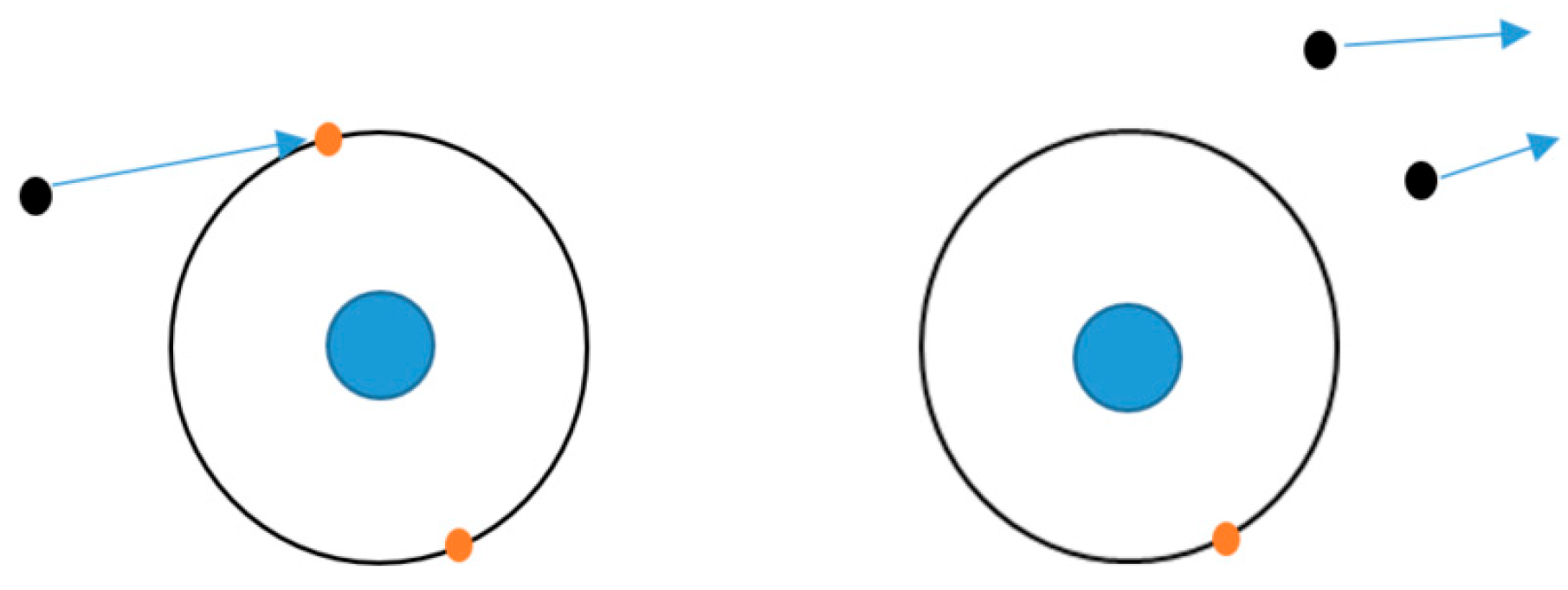
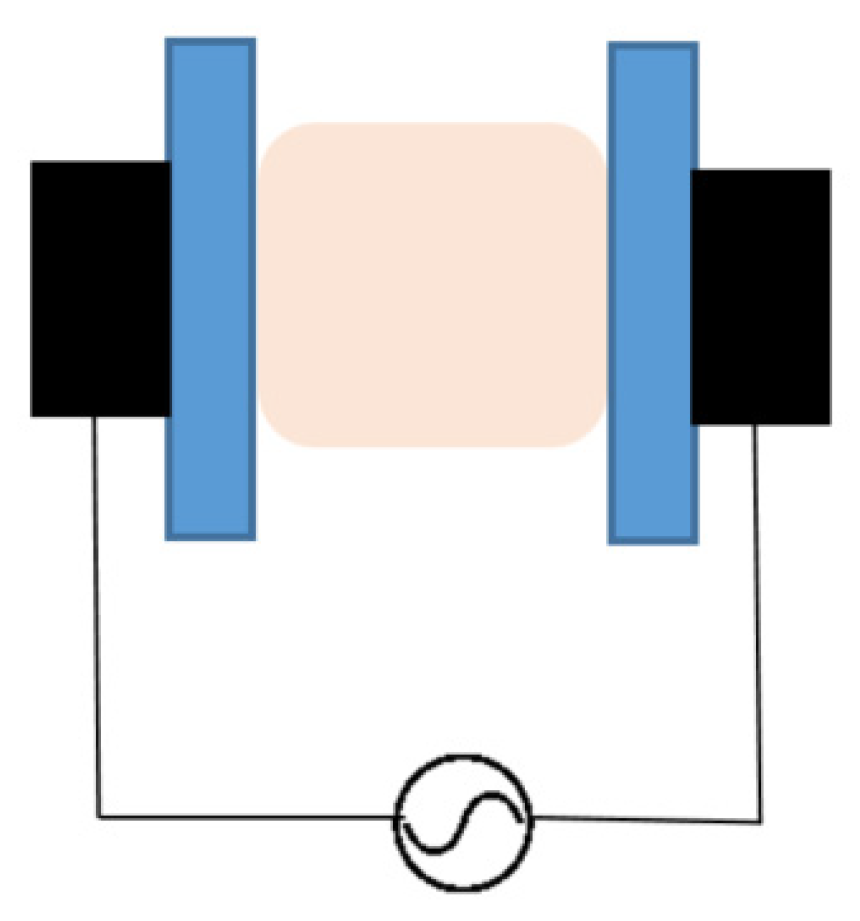
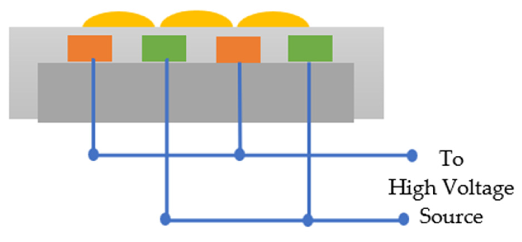


Disclaimer/Publisher’s Note: The statements, opinions and data contained in all publications are solely those of the individual author(s) and contributor(s) and not of MDPI and/or the editor(s). MDPI and/or the editor(s) disclaim responsibility for any injury to people or property resulting from any ideas, methods, instructions or products referred to in the content. |
© 2025 by the author. Licensee MDPI, Basel, Switzerland. This article is an open access article distributed under the terms and conditions of the Creative Commons Attribution (CC BY) license (https://creativecommons.org/licenses/by/4.0/).