


Abstract
Due to the higher power density of silicon carbide (SiC) inverters in electric vehicles (EVs), effectively managing conducted electromagnetic interference (EMI) has become a vital aspect of inverter design. The complex power topology of SiC inverters increases the complexity of different types, phenomena, and mechanisms of conducted EMI, making the selection of appropriate suppression methods more challenging. Many studies have examined the mechanisms of conducted EMI and their suppression techniques. However, the fast switching transients of SiC devices can affect an automotive traction inverter at multiple physical levels, ranging from the gate-drive circuit and isolation interface to the external power terminals. These phenomena are closely related through their common switching excitation and parasitic coupling networks, but they should not all be interpreted as equivalent conducted-emission phenomena. To provide a structured engineering perspective, this review organizes the relevant disturbances using a source–path–victim framework and examines three representative paths: gate-loop crosstalk, common-mode (CM) coupling across the isolated gate-drive interface, and system-level CM/DM-conducted emissions. The corresponding mitigation techniques and their applicability to EV traction inverters are subsequently reviewed.
1. Introduction
With the development of transportation electrification, SiC MOSFETs are increasingly used in electric vehicle traction systems [1]. Compared with conventional Si IGBTs, SiC devices offer lower switching losses and faster switching transitions, which support higher switching frequencies, higher efficiency, and greater inverter power density [2,3,4,5,6,7]. However, the shorter switching transitions also produce higher voltage and current slew rates. These fast transients excite parasitic capacitances and inductances distributed throughout the power stage, gate-drive circuit, isolation interface, and connected power network, thereby increasing the high-frequency excitation of the system and making electromagnetic interference more difficult to control [4,5]. From an EMC perspective, switching disturbances in power electronic systems can appear as both conducted and radiated interference, and recent reviews have summarized radiated EMI mechanisms and mitigation in power converters [8]. This review focuses instead on switching-induced disturbances and conducted EMI associated with SiC traction inverters. The relevant phenomena include internal coupling effects, such as gate-voltage crosstalk and common mode disturbance across the isolation barrier, as well as common mode (CM) and differential-mode (DM)-conducted emissions at the inverter power terminals.
Figure 1a defines the system boundary considered in this review, including the traction inverter, AC cables, motor, and DC network [9]. The SiC switching stage and its gate circuits are the primary design objects. The motor, cables, battery, and vehicle chassis are included only when their impedances, parasitic capacitances, shielding, or grounding connections influence the CM return path or system resonances. Detailed EMC design of the motor, cable, and complete vehicle is outside the scope of this review.
Figure 1.
System boundary and hierarchical organization of switching-induced disturbances in a SiC traction inverter. (a) System boundary of EV traction inverter; (b) locations of three disturbance paths; (c) source–path–victim mapping of gate loop crosstalk (Path A), isolation-interface CM disturbance (Path B), and terminal CM/DM-conducted emissions (Path C).
Although studies have analyzed and improved EMI from the perspective of electric drive impedance modeling and finite element simulation [10,11,12], more focus is placed on the objects affected by EMI and the specific suppression methods in practical engineering. Additionally, the complex structure of the inverter creates many interference paths, which cause disruptions in objects like PWM signals, gate voltages, and three-phase currents. Various interference suppression methods are suited to each disrupted object. This variety of factors makes the existing research lacking in comprehensive analysis and summary of the interference mechanisms and suppression techniques. Moreover, due to space constraints in electric drive systems for EVs, many methods are not appropriate for EV inverters. Current research also lacks a clear summary and analysis of interference mechanisms and suppression methods specific to EV inverters.
From the conventional EMC perspective, conducted emissions at power terminals are generally decomposed into CM and DM components according to their propagation and return paths. The present review retains this conventional classification for system-level terminal emissions. However, fast SiC switching also produces internal electromagnetic coupling that affects the gate-drive and control circuits before the disturbance is observed at an external terminal. Therefore, instead of treating all of these phenomena as equivalent types of conducted EMI, this review adopts the established source, path, and victim framework as the organizing principle [13,14,15]. The disturbance source, coupling path, and sensitive subsystem are identified separately at different physical levels of the traction inverter. Table 1 provides a brief overview of the basic characteristics of the three interference paths.
Table 1.
Classification of the three representative disturbance paths considered in this review.
Based on this framework, three representative disturbance paths are considered, as illustrated in Figure 1b,c. Path A corresponds to the gate-loop level. The high dv/dt and di/dt generated by commutation are coupled through the Miller capacitance and parasitic inductances into the complementary MOSFET gate loop, resulting in positive or negative gate-voltage crosstalk and, in severe cases, false turn-on or excessive negative gate stress. This phenomenon is treated in this review as an internal gate-loop coupling problem rather than a terminal-conducted emission. Path B corresponds to the gate-driver/isolation-interface level. Switching-node voltage transients couple through the parasitic capacitances of the isolated power supply and gate driver, producing CM current and fluctuations of the low voltage side reference potential. This path is therefore identified as an internal common mode disturbance across the isolation interface. Path C corresponds to the inverter/powertrain level, where switching generated CM voltage and DM current excite the distributed impedance network formed by the DC link, busbars, heatsink/chassis, cables, motor, and associated parasitic elements. The resulting disturbances appear as conventional CM/DM-conducted emissions at the inverter and connected-system terminals. In addition, CISPR 25 specifies representative test methods for conducted emissions from automotive electrical and electronic components, in which the artificial network (AN/LISN), harness arrangement, and ground reference plane jointly define the measurement boundary for terminal noise [16]. Consequently, the measured spectrum of the same inverter may vary with the impedance characteristics of the artificial network, harness length and routing, grounding configuration, probe location, and the settings of the detector and resolution bandwidth (RBW) [17]. Moreover, the measured differential-mode noise in motor drive systems may contain a non-intrinsic DM component produced by coupling through the common mode propagation path [18]. Previous studies have shown that incorporating the inverter, DC link, harness, motor, and their associated parasitic parameters into a system-level equivalent model can provide a more accurate description of the propagation paths and spectral characteristics of CM and DM conducted EMI in high-voltage electric drive systems [19].
This review paper aims to provide an overview of the current state of the art in EMI suppression of EV SiC inverters. The paper is organized as follows: Section 2 analyzes the three disturbance paths and the parasitic parameters that govern their responses. Section 3 compares mitigation methods for the gate loop, isolation interface, source modulation, and EMI propagation path. Section 4 discusses emerging design trends associated with 800 V platforms, higher integration, and adaptive EMI control. The resulting framework links each mitigation technique to its dominant disturbance source, propagation path, and engineering constraints.
2. High dv/dt Induced Disturbance and Conducted EMI Mechanisms in SiC Traction Inverters
2.1. Gate Crosstalk in Half-Bridge Circuits
In the inverter topology, Figure 2 shows the equivalent half bridge used to analyze gate-voltage crosstalk. When the lower device turns on while the upper device remains off, the switching node rises and the drain source voltage of the upper device changes rapidly. The resulting Miller current through CgdH enters the upper gate loop. Part of this current charges CgsH, while the remainder flows through the gate impedance, producing a positive disturbance in VgsH. Hereafter, the subscripts H and L denote the upper and lower MOSFETs, respectively; idH and idL are their drain currents, and VdsH and VdsL are their drain source voltages.
Figure 2.
Equivalent circuit of a SiC half bridge for crosstalk analysis.
When the lower device turns off, the direction of the Miller current reverses and a negative VgsH disturbance is produced. The same mechanism applies to the lower MOSFET when the upper device commutates [20].
The above analysis qualitatively explains how crosstalk occurs in half-bridge circuits. To quantitatively evaluate how each parasitic parameter influences the crosstalk voltage, the switching process in the circuit shown in Figure 2 is modeled and analyzed, with the resulting waveforms presented in Figure 3a. The crosstalk effect can be observed in the frequency spectrum of VgsH. If the crosstalk signal has a frequency fcrosstalk, as shown in Figure 3c, the noise in VgsH increases by 10–25% near this frequency, as seen in Figure 3c. The switching transition provides a broadband excitation to the gate loop, whereas the dominant oscillation observed in Vgs is determined primarily by the equivalent gate-loop inductance and capacitance. Therefore, the MHz-range component observed in Figure 3c should be interpreted as a crosstalk ringing or spectral-peak frequency rather than the switching speed. For the circuit conditions reported in [21], the dominant crosstalk-related spectral components occur approximately in the 5–20 MHz range; this range is circuit-dependent and is not a universal characteristic of SiC MOSFET switching.
Figure 3.
Theoretical switching waveforms when the crosstalk occurs. (a) Switching timing diagram. (b) The trend definition of Vgs_on and Vgs_off changes, Vgs_on = Vp_spike − VGate(off), Vgs_off = Vn_spike − VGate(off). (c) Spectrum of VgsH.
To clarify the relationship between the switching waveforms and the analytical model, the crosstalk process in Figure 3a is divided into several characteristic stages. During t1–t2 interval, the dominant disturbance is associated with current commutation and the voltage induced by the common-source inductance. During t2–t3, the low side MOSFET enters the Miller plateau and the rapid variation in VdsL produces a displacement current through CgdH, which becomes the dominant excitation of the high-side gate loop. The subsequent t3–t4 interval describes the natural oscillation and damping of the victim-side gate loop after the switching excitation decreases. The corresponding reverse transition during t6–t8 interval follows the same physical mechanisms with opposite voltage and current polarities.
Specifically, during t1~t2 interval, the lower bridge begins to conduct, the drain-source current idH in the upper bridge decreases, and the drain-source current idL in the lower bridge increases. The decrease in the upper bridge idH (initial value idH0 = Iload) is equal to the increase in the lower bridge idL. The didH/dt generates a voltage drop across the upper bridge inductor LSH, which satisfies Equation (1) for the upper bridge gate-drive loop, and VgsH can be calculated using (1).
where the VGATE(off) is the gate turn-off voltage.
During t2~t3 interval, the lower bridge gate-source voltage VgsL reaches the Miller plateau, causing a rapid drop in VdsL and an increase in the upper VdsH. Based on Kirchhoff’s voltage and current laws, the crosstalk expression (2) can be obtained. Because the VdsH can be expressed in idH (), (2) can be further expressed as (3) [22], in which CXH represents the parasitic capacitance of the SiC MOSFET on the drain-source loop, expressed as (4). During this crosstalk stage, the CdsH and CgsH of the upper bridge charge, leading to a voltage drop across LSH. As a result, VgsH acts as a positive voltage crosstalk.
where CXH denotes the equivalent parasitic capacitance associated with the drain-source loop of the high-side SiC MOSFET. Let Ciss,H = CgsH + CgdH, the homogeneous part of (3) can then be written as:
Comparing this expression with the standard second-order form:
The natural angular frequency of the victim-side gate loop ωH and its dimensionless damping ratio ζH can be derived as shown in (7).
During t3~t4 interval, the VgsH oscillates and decays.
During t6~t7 interval, VgsL decreases to the Miller plateau while VdsL rises and VdsH drops. This causes CdsH and CgsH capacitors to discharge, with VgsH changing in a resembling t2~t3. Therefore, the crosstalk response of VgsH can also be described by (2). In the t7~t8 phase, VgsH fluctuations satisfy (1).
Under inverter operating conditions, if the peak positive crosstalk voltage Vgs_on exceeds the gate threshold voltage of the MOSFET, it causes the upper bridge MOSFET to turn on incorrectly, thus affecting the inverter’s output current. If the peak negative crosstalk voltage Vgs_off exceeds the maximum withstand voltage of the negative gate voltage, the MOSFET may be damaged. Therefore, it is necessary to limit the spikes of the crosstalk voltage. Equation (2) represents a second-order nonhomogeneous differential equation with respect to Vgs, where the response amplitude primarily depends on the forcing terms RgHCgdHdVds/dt and LsHdidH/dt on the right-hand side. The influence of the d2Vds/dt2 term proves negligible due to its substantially smaller coefficient compared to the other terms.
Combining (1) and (2), the factors influencing each parameter in the drive loop on crosstalk are summarized in Table 2. The waveforms of Vgs_on and Vgs_off are shown in Figure 3a.
Table 2.
Impact of circuit parameters on crosstalk voltages.
2.2. Common-Mode Disturbance in Isolated Gate-Drive Circuits
In the SiC MOSFET driving circuit, because of the floating MOSFET source potential, the gate driving signal requires level shifting and isolation of the PWM control signal [26]. The shifted level is generated by an isolated auxiliary power supply, as shown in Figure 4. Here, GND1 and GND2 are the reference grounds for the low-voltage and high-voltage sides, respectively. Since they are not perfectly isolated, Z1 is typically added to represent the parasitic impedance between them. The primary-secondary parasitic capacitance of the isolated power supply, Cps, results from the parasitic capacitance of the isolation device itself, typically in the pF range. The isolated gate driver parasitic capacitance is Ciso. If a voltage disturbance occurs on the high-voltage side, a CM current, ICM, is generated on the low-voltage side. Due to the low voltage of the PWM signal, it might be missed if disturbed [27]. Therefore, Ciso and Cps must be strictly limited to maintain the integrity of the PWM signal.
Figure 4.
Conventional structure gate driver architecture considering parasitic components.
The drain-source voltage slew rate dVds/dt associated with SiC switching produces a rapid variation in the potential between the floating high-voltage-side domain and the low-voltage-control domain. This transient excites displacement currents through the parasitic capacitances crossing the isolation barrier. As illustrated in Figure 4, the main capacitive coupling paths considered here are the primary-to-secondary capacitances of the isolated auxiliary supply and the isolation-barrier capacitance of the gate driver. In the physical circuit, these capacitances are connected to different nodes on the isolated secondary side. Therefore, their contributions are first expressed separately. The total displacement current of isolated auxiliary supply and gate driver can be written as:
where Cps,k denotes the distributed primary-to-secondary capacitance associated with the -th secondary-side conductor, such as the VCC, VEE, and transformer-winding nodes. During a fast CM transient, the isolated DC-DC secondary and the output side of the gate driver form a floating high-voltage-side domain referenced to GND2. With sufficient local decoupling, the differential supply voltages VCC-GND2 and VEE-GND2 vary much more slowly than the CM transition of GND2. Therefore, it can be assumed that dvsec,k/dt = dvdrv,sec/dt = dvGND2/dt. Defining vCM,iso = vGND2 − vGND1, the total CM displacement current injected into the low-voltage side can be approximated as (9). During the commutation transient, GND2 roughly follows the potential at the switch node; thus, vCM,iso ≈ vSW.
Figure 5a shows the fluctuations in the isolated power supply as the device switches. As illustrated in Figure 5b, the spectrum of the coupled CM current is broadband. In the experimental results reported in [28], pronounced spectral components occur approximately in the 5–30 MHz range. These components should be interpreted as dominant CM spectral peaks associated with the switching-edge excitation and the resonant characteristics of the coupling network.
Figure 5.
(a) Isolated supply voltage fluctuation of the upper bridge when the lower bridge is switching. (b) Spectrum of coupled to the low voltage side [28].
In the SiC inverter, the isolated gate driver circuit of the half-bridge topology is shown in Figure 6a. The CHS and CLS capacitors form a low-impedance path. The isolated auxiliary supply is simplified to an LC model [29,30], with an equivalent circuit shown in Figure 6b. If the dVds/dt generated by the high-side or low-side device switch is regarded as the excitation signal, the ratio of the CM currents on the low-voltage side (INoiseGND1) and high-voltage side (INoiseGND2) can be derived as shown in (10) [31,32]. The direction of the current is indicated by the red arrow in Figure 6b.
Figure 6.
Conventional structure gate driver in half bridge: (a) Gate driver architecture considering parasitic components; (b) CM interference propagation paths in equivalent circuit.
The analysis of (9) and (10) shows that the factors affecting the conducted EMI of the isolated gate driver are summarized in Table 3.
Table 3.
Parameters affecting isolated gate driver.
2.3. CM/DM-Conducted Emissions in Electric Drive Systems
In the electric drive system, parasitic capacitance in the heat sink, motor housing, and other components, along with parasitic inductance in the connecting wires, create an equivalent circuit shown in Figure 7a. The voltage and current transitions generated during MOSFET commutation constitute the principal high-frequency excitation sources. Based on the noise propagation path, it can be classified into CM interference (red path) and DM interference (blue path), as indicated in Figure 7a. Along the CM path, switching voltage excites displacement current through the parasitic capacitances between the inverter, motor, cable, and chassis. The drain-source voltage of the Q1 MOSFET during inverter operation is shown in Figure 7b [34], while the DC bus current is depicted in Figure 7c.
Figure 7.
Conducted EMI modeling of three-phase power converters at high frequencies: (a) Equivalent circuit for CM and DM coupling paths. (b) Switching voltage Vds of Q1. (c) IDC and IDM caused by switching of each phase on the DC side [34].
The inverter’s CM voltage VCM is shown in Figure 7b. Variations in VCM during MOSFET switching can cause interference in the electric drive system by creating a CM interference loop through the parasitic capacitance. The equivalent circuit for single-phase CM interference is illustrated in Figure 8a [35], where parasitic elements such as the distributed inductance of the AC cables, MOSFET drain-source capacitance, and inter-cable capacitance are combined into Zeq/3. Additionally, the CM model of the electric drive system can be simplified to the circuit in Figure 8b [36], with the symmetry of the structure allowing a quantitative description of VCM and ICM using (11).
Figure 8.
(a) CM circuit configuration for a part of the inverter in frequency domain [35]. (b) CM equivalent schema. (c) CM source based on standard PWM wave. (d) CM Noise Spectrum Schematic.
The MOSFET switching equivalent voltage source VCM can be approximated by a periodic trapezoidal pulse with finite rise and fall times, as shown in Figure 8c. For frequency-domain analysis, VCM is represented by a truncated complex Fourier series. To avoid the singularity at n = 0, the DC component is treated separately from the nonzero harmonic components:
and for n ≥ 1,
where is the DC-link voltage, Ts is the switching period, ton and toff denote the starting instants of the rising and falling transitions, respectively, and tr and tf are the corresponding rise and fall times. denotes the harmonic order, N is the truncation order of the Fourier series, and Sa(x) = sin (x)/x [37]. The exponential terms describe the phase positions of the rising and falling edges, whereas the Sa(·) terms determine the attenuation of the high-order harmonics associated with the finite switching transition times. Figure 8d shows that the CM conducted EMI is distributed over a broad frequency range and generally attenuates with increasing frequency, while a resonance peak remains around 10 MHz due to the frequency-dependent CM propagation network.
DM interference is represented by a differential-mode current IDM on the DC bus side of the electric drive system, as shown in Figure 7c. The equivalent circuit for DM interference in a single phase is illustrated in Figure 9a [35]. The load inductance displays high impedance at high frequencies and can be considered open-circuited; therefore, it is not shown in the diagram. Additionally, the design of the DC bus must account for the mutual inductance between the DC bus and the phase wiring harness. For the equivalent current source IDM, it can be similarly described as a sequence of square waves, as shown in Figure 9b, with its expression satisfying (14) assuming tr = tf. As shown in Figure 9c, the DM conducted-emission spectrum extends over the full 150 kHz–30 MHz band. The measured curve rises in the MHz range and exhibits two pronounced resonance peaks, reflecting the frequency-dependent resonant characteristics of the motor-drive impedance network, before decreasing at higher frequencies. This indicates that the observed DM spectrum is determined jointly by the equivalent PWM current source and the system impedance network. Similar source-network analytical prediction concepts have also been reported for SiC motor-drive EMI analysis [38].
where D is the duty cycle, T is the inverter switching period, Iamp is the current amplitude, and n represents the harmonic order. Figure 10 summarizes the different roles of the switching-edge and PWM parameters in the spectrum of an idealized periodic pulse waveform [39]. As shown in Figure 10a, the noise attenuation characteristics at both low and high frequencies can be described by the corner frequency, where fc is expressed as in (15) [33]. As shown in Figure 10b, reducing the tr and tr, or equivalently increasing the voltage/current slew rate, shifts the transition-related corner frequency toward higher frequencies. Consequently, appreciable switching-edge spectral content extends further into the MHz range. This effect is distinct from changing the switching frequency fs. As illustrated in Figure 10c, fs determines the spacing and locations of switching-related harmonics, whereas the amplitudes of individual harmonics depend on the pulse waveform and modulation strategy. The duty ratio D further changes the harmonic coefficients rather than uniformly increasing all spectral components as shown in Figure 10d.
Figure 9.
(a) DM circuit configuration for a part of the inverter; (b) DM source based on standard PWM wave; (c) DM Noise Spectrum Schematic.
Figure 10.
Effects of pulse waveform parameters on the spectral envelope (a) representative spectrum; (b) transition time; (c) switching frequency; (d) duty ratio [39].
For short interconnections and relatively low frequencies, the lumped parameter models shown in Figure 7, Figure 8 and Figure 9 are generally sufficient to describe the dominant CM and DM propagation paths. As the switching transitions of SiC devices become faster and the motor cable length increases, however, cable propagation delay can no longer be neglected, and the high-frequency behavior is more appropriately represented using a distributed parameter model. For a cable characterized by the per unit length parameters , , , and , the characteristic impedance, propagation constant, and load-end reflection coefficient can be expressed as in (16).
Accordingly, the cable length, characteristic impedance, and high-frequency impedance at the motor terminals determine not only the reflected overvoltage but also the resonant frequencies of the CM propagation network. Experiments on SiC motor drives have shown that fast switching edges and cable impedance mismatch can significantly affect both motor terminal overvoltage and switching loss [40]. More recent approaches, including active reflection cancelation [41] and the motor-side smart coil [42], exploit the propagation characteristics of the cable and process only the transient energy associated with commutation. This principle can reduce the size and power handling requirements of conventional output filters.
Cable shielding also changes the distribution of CM current. A study of a complete SiC EV powertrain showed that the length and type of the AC cable, as well as whether the DC cable is shielded, can substantially alter the system CM EMI spectrum [43]. The shield increases high-frequency coupling between the conductors and the vehicle body or enclosure. Although this can reduce the potential at certain motor terminals, it may simultaneously increase the CM current returning through the chassis. For example, in experiments with a 3 m cable, replacing an unshielded cable with a shielded cable increased the stator to ground current by approximately 25%, while the bearing voltage and bearing current decreased by about 5%. When the shielded cable length was further increased from 3 m to 10 m, the bearing voltage decreased by approximately 11%, whereas the stator to ground current increased by about 14% [44]. Related review studies have likewise indicated that cable shielding can mitigate some rotor- and bearing-related disturbances while increasing the stator to ground the CM current [45].
The influence of motor and enclosure parasitic parameters is also strongly frequency-dependent. Distributed capacitances between the winding and stator, rotor and bearings, and motor enclosure give rise to multiple resonances in the CM and DM impedances within the MHz range. Recent broadband impedance modeling has extended the valid characterization range of motor CM, DM, and phase to ground impedances from 100 Hz to 120 MHz, with the average magnitude error maintained within approximately 2.96 dB for motors of three different power ratings [46]. For a complete PMSM drive system, the experimental and modeling results in [47] showed that, on the investigated platform, the CM current in the range of approximately 150 kHz to 3 MHz was mainly governed by the motor impedance, whereas cable and inverter parasitic paths became increasingly dominant at higher frequencies. This result also indicates that the relative importance of individual system components cannot be represented by a fixed ranking across the entire EMI frequency range.
As traction systems become more highly integrated, parasitic elements that were previously distributed among separate subsystems become more strongly coupled. A recent study of an EV all in one motor drive module [48] showed that the stray inductance of the DC busbar and the capacitances of a multiport bus structure can form additional CM resonance paths, and that the dominant parameters can be identified through sensitivity analysis. The parasitic capacitance between the switching node of the power module and the heatsink or enclosure also follows the approximate relationship iCM,pkg ≈ Csw-chdvsw/dt. By optimizing this parasitic capacitance in a SiC power module, the experimental study in [49] achieved an approximately 17 dB reduction in CM current while simultaneously reducing the total switching loss by 28.5%.
In automotive traction inverters, the PWM switching frequency fs is typically in the order of tens of kilohertz, while SiC devices permit higher switching frequencies than conventional Si IGBTs because of their reduced switching losses [50]. The discrete spectral components generated by PWM occur at fs and its harmonics nfs, whereas the finite rise and fall times of individual switching transitions determine the spectral envelope at high frequencies. In addition, parasitic LC networks in the module, busbar, cable, motor, and chassis paths can produce resonances in the MHz range. Consequently, MHz range EMI components should be attributed to the combination of fast-edge excitation and system resonances [37]. Table 4 lists some of the factors that affect the frequency spectrum of conducted EMI noise.
Table 4.
Physical roles of switching parameters in the conducted-EMI source spectrum.
3. Mitigation of Switching-Induced Disturbances and Conducted EMI
3.1. Crosstalk in Half-Bridge Circuits
Section 2.1 shows that the primary excitation of gate crosstalk in a half-bridge circuit is the rapid voltage and current transition associated with SiC MOSFET commutation. The resulting dVds/dt and did/dt are coupled into the complementary gate loop through the Miller capacitance and parasitic inductances, producing gate-voltage disturbance.
The current crosstalk suppression methods for half-bridge circuits can be categorized into two types. The first method targets the propagation path [56] and reduces interference by adding Miller clamping circuits, which absorb the energy of the Miller current flowing through the gate. The second method addresses the interference source itself by actively adjusting the gate driving capability of the SiC MOSFETs based on operating conditions, which helps to reduce dVds/dt and suppress gate-voltage crosstalk in the complementary MOSFET.
3.1.1. Miller Clamp Circuit
Miller clamp circuits are among the most common and cost-effective methods for addressing crosstalk issues. These circuits establish a low-impedance path between the gate and the source, either bypassing the Miller current or clamping the gate voltage to the negative rail voltage. Typically, the driver IC includes an integrated Miller clamp circuit, though it can also be implemented using discrete components. Miller clamps are categorized based on the triggering method into two main types: passive [57,58,59,60,61,62,63] and active [64,65].
- Active Miller clamp
Active Miller clamp circuits usually regulate an auxiliary transistor using a specific control strategy that adjusts the external gate resistor or pulls the gate voltage down to a negative drive voltage or ground. A common method is to compare the indicated parameter with a reference voltage, which then produces a control signal [66]. The parameter typically monitored in active Miller clamp circuits is the gate voltage, with a reference voltage that does not surpass the gate threshold voltage [67].
Another method for active Miller clamping is clamp control based on the switching logic signals of SiC MOSFETs. In [68], the gate auxiliary circuit includes two diodes and two auxiliary MOSFETs with opposing logic, whose control signals must be synthesized from the switching logic signals of the SiC MOSFETs. The auxiliary circuit in [69] and its logic signals are shown in Figure 11. This setup introduces an auxiliary capacitor to help share charging and discharging currents flowing through Cgs. The auxiliary capacitor provides a low-impedance path while increasing the gate charge [70].
Figure 11.
Gate impedance adjustment circuit using buffer capacitor: (a) circuit schematic; (b) corresponding logic signals of main device and auxiliary transistor [69].
- 2.
- Passive Miller clamp
In passive Miller clamp circuits, the timing of intervention is determined by changes in the monitored parameters of the drive loop, which depends on passive elements and auxiliary transistors. Ref. [57] proposes a resistor-capacitor-diode (RCD)-based passive clamp circuit as shown in Figure 12. The RCD circuit is placed between the gate and source terminals. It operates as follows: when positive crosstalk occurs, as shown in Figure 12a, the Miller current flows through Rexth, making Qclp conductive, which creates a low-impedance loop path and charges the Cclp capacitor, helping to reduce the influence of the Miller current on Vgate. When negative crosstalk occurs, it is observed to charge Cgd via the Cclp capacitor and diode Dclp, as shown in Figure 12b, which helps suppress the crosstalk. Based on similar principles, RCD-derived level-shifting and auxiliary clamping circuits have been developed to generate an appropriate negative turn-off voltage and/or provide a low-impedance path for the Miller current, thereby limiting the gate crosstalk voltage [63,71,72,73,74,75]. Active clamping methods triggered by the switching transient provide another implementation route [64].
Figure 12.
Passive Miller clamp circuit: (a) positive crosstalk; (b) negative crosstalk [57].
3.1.2. Active Gate Driver
Active gate drivers (AGDs) regulate the switching trajectory by adjusting gate voltage, gate current, resistance, or capacitance according to the switching state or measured electrical variables. Their main design objective is to limit crosstalk, overshoot, and ringing while controlling switching loss [76]. The methods reviewed here are grouped according to the controlled gate parameter and the use of open or closed loop feedback.
- AGD methodologies based on parameter tuning
In the case of SiC MOSFETs, the switching speed can be appropriately limited to reduce crosstalk. Based on differences in adjustment parameters, the AGD methods can be classified into four types.
VGSDVC (Variable Gate-Source Driving Voltage Circuit): The purpose of the VGSDVC is to directly adjust the gate-voltage trajectory during the switching process of SiC MOSFETs. Conventional implementations generally use predetermined gate-voltage levels or trajectories [77,78]. The AGD proposed in [79] uses three cascaded gate-drive buffers as multilevel selectors, as shown in Figure 13. The microcontroller controls access to the impedance and n resistors, which can be adjusted in 2n levels. This approach aligns with the principles of DAC and is implemented in two ways: one involves using an external resistor network as described above; the other employs an internal programmable amplifier, with its gain adjusted via software.
Figure 13.
Active gate drive with adjustable gate voltage, the circuit consists of microcontroller, adjustable voltage regulator, voltage selector and current absorption circuit [79].
CGCC (Controlled Gate Current Circuit): The controlled gate current method mainly controls gate charge injection by adjusting the charge and discharge currents to the input capacitor Ciss. Its functions have been validated in [80,81,82,83,84]. A common approach involves connecting a current source branch to the gate, as shown in Figure 14. When the peak dVds/dt exceeds the threshold Vref1 set by the microcontroller, VQ1 conducts, and the current mirror output ic is injected into the gate branch of the DUT [85]. The commanded gate current can also be generated from a programmable voltage stage, allowing the current level to be adjusted during different switching intervals.
Figure 14.
Double closed-loop self-regulating AGD, consisting of control signal generating circuit, voltage controlled current source, peak sampling system and dVds/dt sampling circuit [80].
VGRC (Variable Gate Resistance Circuit): As discussed in 2.1, increasing the gate resistance for the Miller plateau interval effectively reduces the dVds/dt of the MOSFET while also setting an appropriate resistance value of interference devices, which helps lower gate-voltage crosstalk. The most common approach involves using a combination of multiple gate resistors and switches [86,87,88]. As shown in Figure 15, the microcontroller detects the switching stage by monitoring dVds/dt and adjusts the gate resistance accordingly by controlling the switching signal at various MOSFET switching stages.
Figure 15.
Typical circuitry of variable gate resistance method [89].
VGSCAC (Variable Gate-Source Capacitor Assisted Circuit): The variable gate capacitance method controls the Miller current shunt by adjusting the value of Cgs/Cgd, which regulates the Miller plateau duration and enables the regulation of switching speed. However, a Cgs that is too large can lead to increased switching delays in the SiC MOSFET and can also result in peak gate currents that exceed the gate oxide stress limit [90]. To prevent this, it is necessary to adjust the timing of connecting the external gate capacitor to the gate-source using a control switch, as shown in Figure 16 [91,92]. Additionally, placing the gate resistor in parallel with the speed-up capacitor [93,94], as shown in Figure 16, can increase the MOSFET switching speed, reduce switching losses, and suppress surge voltages.
Figure 16.
Typical variable input capacitance active gate driver structure.
- 2.
- Control Strategies for AGD
Ensuring that power devices operate optimally with open-loop methods [86,95,96] remains challenging. Closed loop AGD introduces sensing and feedback so that the switching trajectory can be adjusted during operation [97]. The principle of AGD based on feedback control is illustrated in Figure 17 [98].
Figure 17.
Block diagram of the measurement-based control [98].
By compensating for the error between the reference and feedback signals, the switching process can be actively controlled using the methods described above for adjusting the gate loop parameters [99]. Due to the rapid switching speed of SiC MOSFETs (10~100 V/ns), high resolution (sub-nanosecond delay) is also necessary for the acquisition circuit [100]. With a sufficient sampling rate of the sensing circuit and ADC, dVds/dt and did/dt are used as the indicated parameters to be controlled by PI controller to eliminate the system’s steady-state error [101].
It has been demonstrated that AGD feedback circuits can worsen crosstalk [102]. To address this, ref. [103] analyzes the mechanism of crosstalk caused by feedback circuits using the equivalent capacitance model and proposes a Crosstalk Suppression (CTS) circuit. As shown in Figure 18, the CTS effectively blocks the Voltage-Control-Current-Source (VCCS) when the MOSFET is in the freewheeling state, thus preventing crosstalk.
Figure 18.
Circuit diagram of the closed-loop ACSD with CTS to suppress crosstalk [103].
This section covers techniques for crosstalk suppression in half-bridge circuits. Many manufacturers are now offering gate drivers with AGD functionality. To give readers a complete overview of inverter design, Table 5 provides a clear summary of EMI suppression methods between half-bridges and their current uses in commercial gate drivers.
Table 5.
Comparison of gate loop crosstalk mitigation strategies for SiC half-bridge circuits.
3.2. Common-Mode Current Suppression in Isolated Gate Driver
3.2.1. Internal Structure of Isolated Gate Driver
Equation (9) shows that CM current across the isolation interface is directly proportional to the effective coupling capacitance. For transformer-based auxiliary supplies, this capacitance is governed mainly by the overlap area, spacing, and electric field distribution between the primary and secondary windings. Planar PCB transformers can therefore be optimized to reduce coupling capacitance while satisfying power density, insulation, and loss requirements [104,105,106]. Ref. [107] proposes a PCB embedded isolated auxiliary supply that takes the transformer volume, loss, and isolation capacitance as optimization objectives and is designed through a Pareto optimal solution surface.
Additionally, one of the most effective ways to optimize the integrated structure of the PCB is to add a Faraday shield [108], whose principle is shown in Figure 19. In this method, a properly grounded conductive sheet is placed at an appropriate location between the windings to shunt the CM current.
Figure 19.
CM-current flow path in transformers. (a) Without shielding (b) with grounded electrostatic shield. (c) PCB-based winding structure with shielding layer.
3.2.2. External Structure of Isolated Gate Driver
Designing a transformer reduces parasitic coupling capacitance and improves CM rejection, but PCB layout and additional design costs must be considered. Although commercially available isolated auxiliary power supplies or gate drivers can enhance integration, parasitic coupling capacitance remains a key limitation. Based on this, the following section summarizes how to mitigate CM interference of the gate driver through external structural improvements.
Adding a CM choke on the low voltage side is a common way to suppress CM interference in gate drivers. The selection of the choke needs to take into account both CM and DM characteristics [109,110]. Figure 20 illustrates that when p = C, ZC represents the CM impedance, and Kc is the coupling coefficient with KC = 1. Moreover, when p = D, ZD represents the DM impedance, and KD is the coupling coefficient with KD = −1. This modeling decouples CM interference and DM interference.
Figure 20.
Equivalent circuit for a single-phase choke. (a) Common-mode and differential-mode decomposition of the choke impedance, where ZC and ZD represent the corresponding modal impedances (KC = 1, KD = −1). (b) Equivalent circuit of the unit section Zpi. (c) Cascade representation of the overall choke model.
The impedance of the choke to CM interference can be expressed as (17).
where NC is the number of choke winding turns, which corresponds to the number of impedance blocks Zpi in Figure 20c; RCI is the core resistance to characterize the hysteresis and eddy current losses; Cci is the capacitance inside the winding; Lci is the winding inductance; and R0 is the external resistance. The curve of with f usually has one or more resonance peaks, so the choke achieves better suppression only for CM noise in a specific frequency range.
In the conventional half-bridge gate driver structure illustrated in Figure 6a, each driver is powered by a discrete, isolated power supply. As discussed in Section 2.2, it is necessary to create a path with reduced CM interference for INoiseGND2, which helps direct CM current back to the high-voltage side, thereby reducing interference on the low-voltage side signal. Based on this principle, a common approach is to cascade multiple isolated supplies to enable CM-current shunting, as shown in Figure 21a [28]. As seen in the current path diagram in Figure 21b, this topology achieves gradual attenuation of CM through a series cascading configuration of power supply branches.
Figure 21.
Cascaded gate driver in half bridge. (a) Cascaded gate driver power supply configuration. (b) Equivalent circuit for Cascaded gate driver [28].
Table 6 compares representative CM-current mitigation strategies at the isolated gate driver interface in terms of the controlled coupling parameter, reported implementation performance, and principal engineering constraints.
Table 6.
Comparison of CM-current suppression strategies for isolated gate driver interfaces.
3.3. EMI Control Strategy for Electric Drive Systems
Based on the analysis presented in Section 2.3 regarding the EMI generation mechanism of the electric drive system, it can be concluded that the suppression method can be derived from both the interference source and the propagation path.
3.3.1. Conducted EMI Suppression Techniques Based on the EMI Source
PWM strategies influence conducted EMI mainly through two mechanisms. First, variations in switching frequency fs, frequency deviation ∆fs, and switching sequence redistribute the discrete spectral components around nfs and their sidebands [37,51,52,113,114,115,116,117,118]. Second, PWM modifies the common mode voltage (CMV) waveform, including VCM,pk, VCM,RMS, and the number or magnitude of CMV transitions, thereby affecting the common-mode current through iCM = Cp·dvCM/dt. These mechanisms lead to three main classes of PWM based mitigation: spectrum spreading, CMV optimization, and multiobjective modulation [116,117,118,119,120,121,122,123,124,125,126,127,128,129,130,131,132]. Modulation also affects current harmonics, switching losses, and control performance. For example, variable switching frequency PWM (VSFPWM) changes the effective sampling and modulation behavior of the current loop, which can alter the bandwidth and phase response of the current controller [133].
Spectrum spreading methods redistribute the discrete peaks concentrated around and their sidebands over a wider frequency range by varying the carrier frequency or switching instants [134]. Experimental results in [135] at a modulation index of m = 0.8 show that constant switching frequency PWM (CSFPWM) produces a pronounced spectral peak of nearly 100 dBμA around 150 kHz. Random or periodic carrier modulation substantially reduces these discrete peaks, as shown in Figure 22, although the noise floor increases in parts of the 150 kHz–2 MHz range. Experiments on a WBG traction inverter in [117] similarly showed that spread spectrum modulation reduced the common mode conducted EMI peak at 160 kHz by only about 2 dB, whereas an alternative topology with an auxiliary switching leg achieved a reduction of approximately 25 dB on the same platform. Spectrum spreading is therefore most useful for discrete peaks near the carrier and its sidebands; the measured benefit remains sensitive to spreading depth, network resonances, and receiver bandwidth.
Figure 22.
Qualitative comparison of various PWM schemes: CSFPWM, VSFPWM, RPWM, Normal distribution PWM(NDPWM) with modulation index 0.8 [135].
For direct suppression of common mode excitation, recent studies have increasingly optimized the CMV waveform and switching vector sequence. Representative approaches include active zero vector PWM, phase clamping PWM, zero sequence voltage injection, and optimized vector sequencing. These methods reduce CM excitation by limiting switching states with high CMV or reducing the number of CMV transitions. In [122], a 240° clamped SVPWM strategy for EV/HEV traction systems was experimentally evaluated on a 10 kW platform. Compared with conventional CSVPWM, it reduced both the CMV peak and the number of CMV pulses per switching period by 66.7%, lowered by 21%, and reduced switching loss by about 85%, while maintaining a similar current THD at the maximum speed. In [123], zero sequence voltage injection was used to eliminate pulse overlap regions responsible for large CMV excursions, reducing the CMV amplitude by 50% and the number of CMV pulse edges by approximately one third. Reference [128] further showed that pulse position optimization can coordinate CMV suppression and current quality without substantial degradation of the output performance. CMV optimization directly reduces the source excitation and can be coordinated with switching loss and current quality.
To account for the influence of dead time and switching loss on CMV suppression, ref. [119] proposed modified single edge modulation (MSEM). Active voltage vector combinations are selected according to the sector, and their sequence is rearranged to reduce switching loss. The carrier frequency is also varied according to the output current phase to address differential-mode-conducted EMI. Because dead time can reintroduce CMV spikes during commutation, the pulse sequence is further corrected according to the phase current direction at the switching instant. Similarly, ref. [129] reconfigured the voltage vector sequence of a three phase PMSM drive and experimentally verified the resulting reduction in CM excitation and conducted EMI. Since the effectiveness of such methods depends on both dead time and switching loss, the optimal vector sequence remains operating point-dependent. Reference [121] proposed a software modulation method based on delay compensation. By iteratively calibrating the commutation instants of different bridge legs, CM-current pulses generated by adjacent legs are made to cancel as far as possible. The method reduced common mode conducted EMI by about 30 dB at 160 kHz and maintained approximately 15–20 dB attenuation over several MHz. It requires no additional high power filtering branch, but its performance depends on accurate commutation delay calibration and on the adopted four-leg topology.
For emerging winding configurations, the CMV generation mechanism also depends on the inverter topology [132]. For a series end winding motor drive (SWMD), ref. [120] showed that the motor-side and inverter-side CMVs differ because of the asymmetric winding connection, and proposed constant CMV PWM (CCMV-PWM) and reduced CMV PWM (RCMV-PWM). CCMV-PWM is mainly suited to the low modulation range and suppresses CMV variation by selecting voltage vectors with the same common-mode potential. RCMV-PWM expands the available vector set and can cover the full modulation range. The two strategies therefore provide complementary tradeoffs between modulation range and CM suppression. For multi inverter motor drives, ref. [130] proposed a discontinuous PWM strategy that eliminates the phase to ground CMV of a dual unit PMSM drive under ideal switching conditions by restricting the switching states that generate common mode potential. Dead time, however, still introduces short CMV spikes and therefore requires compensation.
As the coupling among CMV, switching loss, and current quality becomes more pronounced, recent studies have employed optimization-based PWM and model predictive control (MPC) to coordinate multiple objectives. In [124], low CMV virtual voltage vectors were combined with a variable DC bus for an EV PMSM drive, improving CMV, current harmonics, and switching frequency characteristics in the low-speed region. Reference [131] reconstructed the candidate voltage vectors and prediction process so that MPC for a multilevel inverter inherently suppresses CMV, avoiding the tuning problem associated with an additional CMV weighting factor. Ref. [125] further address the high dv/dt issue in SiC PMSM drives, both CMV and motor-terminal DMV are incorporated into the pulse pattern design; accounting for dead-time effects, various candidate pulse sequences are constructed based on the modulation index. This method reduces the peak line voltage at the motor terminals by approximately one-third compared to two RCMV-MPC baseline methods. Under operating conditions of 500 r/min and 10 N·m, the torque ripple is approximately 0.13 N·m and the current THD is 14.02%, all without increasing the switching frequency or computational burden.
Recent PWM optimization has therefore evolved from a single CMV amplitude metric toward multidimensional criteria that include CMV transitions, common-mode current, differential-mode voltage, THD, switching loss, and real-time computational demand. This is particularly important for SiC traction inverters, where fast switching makes the final EMI response more sensitive to dead time, parasitic parameters, and motor cable impedance. Consequently, CMV reduction and conducted noise attenuation reported for the same modulation strategy on different test platforms should not be ranked directly without considering the corresponding operating and measurement conditions. Table 7 summarizes the operating principles, experimental results, and main constraints of representative PWM methods. From an engineering perspective, spectrum spreading requires no modification of the power topology and is well suited to reducing discrete peaks around the carrier and sidebands. CMV optimized PWM directly reduces common mode excitation and can coordinate switching loss through appropriate vector and sequence design. MPC and optimized pulse patterns provide greater flexibility for multiobjective coordination, but require more detailed models, computational resources, and operating point calibration. For broadband conducted noise amplified by resonances in the cable, motor, and parasitic network, modulation optimization should therefore be combined with CM/DM filtering and common-mode return path design.
Table 7.
Representative PWM strategies for EMI and CMV oriented optimization.
Additionally, Figure 23 illustrates the three main source-side PWM mitigation mechanisms. Spectrum spreading redistributes discrete switching harmonics, CMV-oriented modulation reduces common-mode excitation by reshaping the CMV waveform and switching sequence, and multi-objective modulation coordinates EMI suppression with switching loss, current quality, and other operating constraints.
Figure 23.
Source-side principles of PWM-based conducted EMI mitigation. (a) spectrum spreading using periodic and random PWM; (b) CMV-oriented modulation and the resulting reduction in common-mode current; (c) multi-objective modulation considering EMI, switching loss, and current THD.
3.3.2. Method Based on EMI Propagation Paths
Filtering strategies in electric drives can be compared according to installation location, noise mode, and implementation form. DC filters limit noise propagation toward the high-voltage DC network, whereas AC filters primarily control the CM return path through the cable and motor and can also reduce motor terminal voltage stress.
On the DC side, CM current returns mainly through parasitic capacitances to the chassis, whereas DM noise circulates between HV+ and HV−. A CMC and are therefore typically used for the CM path, while DM inductors and CX form LC or Π networks for DM attenuation.
Designing the filter to provide a uniformly large insertion loss over the entire specified frequency range can readily lead to overdesign. Ref. [136] compared two DC-side filter designs for a PMSM drive. In the conventional design, an insertion loss of approximately 60 dB was specified over a broad frequency range from 150 kHz to 108 MHz. By contrast, a resonance targeted design focused on the dominant resonances near 1 MHz and 30 MHz. While satisfying the required attenuation, the resulting filter volume was reduced to approximately one quarter of that of the conventional design. In subsequent work, the source impedance of the motor controller was incorporated into the filter design, and compliance with CISPR 25 Level 3 was experimentally demonstrated [137]. These results indicate that the design margin of DC-side common-mode and differential-mode filters should be determined according to the actual frequency ranges of excessive emissions together with the source and load impedances.
When the size of a large CMC and the leakage current associated with CY become limiting factors, active and hybrid filters can reduce the required passive inductance or capacitance, at the cost of auxiliary loss, control bandwidth, and stability requirements. Ref. [138] developed a hybrid common mode filter for an EV traction inverter by cascading an active compensation stage with a high-frequency passive branch. Its capability to suppress DC-side common-mode noise was experimentally verified under high current electric drive operation. Ref. [139] employed the common mode impedance of the motor to construct a transformerless active EMI filter, in which voltage sensing and current compensation were used to reduce DC-side common-mode noise.
On the AC side, common-mode noise is mainly excited by high-frequency voltage variations that occur simultaneously at the three phase terminals with respect to the chassis. The resulting current returns through the motor housing, cable shield, and parasitic capacitances between the windings and ground. A typical three phase AC-side common-mode filter is shown in Figure 24. The three phase conductors pass through or are wound around a common magnetic core to form a CMC, while CY or the cable shield is used to control the high-frequency common-mode return path. In comparison, differential-mode components on the AC side mainly appear in the phase to phase voltages and currents. LC and LCL filters, as well as output dv/dt filters, can be used to suppress high-frequency differential-mode components and reduce terminal voltage stress caused by cable reflections.
Figure 24.
Typical configuration of filter in electric drive systems.
Recent studies on AC side filtering for SiC electric drive systems have placed particular emphasis on reflected waves and high dv/dt under long cable conditions. Ref. [140] proposed a band stop dv/dt filter designed around the cable resonance. By introducing selective impedance near the dominant reflected wave frequency, the filter achieved motor terminal voltage suppression comparable to that of active solutions while maintaining lower loss and smaller volume. Ref. [141] employed a T type active dv/dt filter and experimentally limited the motor terminal voltage peak to approximately 1.13–1.15 pu under a 400 V DC bus, a 20 kHz switching frequency, a 2.2 kW motor, and a 12.5 m cable. Because these methods primarily address AC terminal insulation stress and reflected waves, their performance metrics differ from those used for CISPR-based conducted emission measurements at the DC terminals. Therefore, their results should not be directly compared numerically with attenuation values reported in dBμV or dBμA.
In practical traction systems, AC side EMI mitigation must also consider cable shielding and chassis return paths. Shielded cables can reduce the common mode potential at the motor terminals while simultaneously increasing common-mode current flowing through the chassis [43,44]. Therefore, filter placement should be coordinated with the shield termination and chassis connection strategy. In addition to conventional passive approaches, ref. [142] placed an active EMI filter in the motor frame to ground branch and suppressed DC-side common-mode noise by modifying the impedance of the grounding loop. Accordingly, the central objective of AC-side propagation path optimization in vehicle applications is to control the closed path of common-mode current and the impedance associated with that path.
In passive filtering, the CMC remains the core component for suppressing CM current. A typical three-phase AC-side CM filter is shown in Figure 24 [143], where the three phase conductors are wound on a common magnetic core to form a CM choke, and the CY capacitors provide a controlled high-frequency return path to the motor casing or chassis ground. Under CM excitation, the phase currents flow through the choke windings in the same magnetic direction, so their magnetomotive forces add in the magnetic core [144,145]. In the linear small-signal region, the inductive behavior of a CM choke can first be described using a magnetic-reluctance model, in which both the material permeability and the geometry of the magnetic flux path determine the resulting inductance [146]. The magnetic reluctance of a general core can be expressed as (18).
where A(l) is the local core cross-sectional area, μ0 is the permeability of free space, and μ0′(f) is the effective real permeability at frequency f. According to Ampere’s law, the magnetomotive force produced by an m-winding choke can be expressed as (19).
and the corresponding core flux is Φ = F/Rm. Therefore, the flux linkage of winding i is shown as (20).
where the self and mutual inductance terms are determined by the common magnetic path. For m identical windings carrying the same CM current, i1 = … = im = iCM, the effective CM inductance seen by each winding is LCM,ph = Ls + (m − 1)M, in which Ls is the self-inductance of one winding and M is the mutual inductance between two windings. For a symmetrical three-phase choke, LCM,ph = Ls + 2M.
With tight magnetic coupling and small leakage inductance, M approaches the magnetizing component of Ls, so the CM inductance is substantially enhanced because the three phase magnetomotive forces reinforce each other. In contrast, under balanced differential-mode excitation, ia + ib + ic ≈ 0, and the net core flux is strongly reduced. For engineering calculations, the magnetizing inductance of one winding can be conveniently written using the effective core parameters as (21).
where NL is the number of turns per winding, Ae is the effective magnetic cross sectional area, and le is the effective magnetic path length. For a toroidal core with inner radius ri, outer radius ro, and axial height hc, Ampere’s law gives H(r) = NLi/(2πr). Integrating the resulting magnetic flux over the radial core dimension yields:
At higher frequencies, the choke should be described by its frequency-dependent impedance [147,148]. If the core permeability is written as μ*(f) = μ′(f) – jμ″(f), the imaginary component represents magnetic loss, while winding capacitance, leakage inductance, and other parasitic effects introduce self-resonance and modify the CM insertion impedance [144,149]. Therefore, a high value of μ′ can increase the low- and mid-frequency CM inductance, but the usable EMI attenuation range also depends on μ′(f), μ″(f), core geometry, winding configuration, parasitic capacitance, flux density, temperature, and DC-bias conditions. The relevant characteristics of commonly used magnetic materials are summarized in Table 8.
Table 8.
Comparison of magnetic core materials for EMI chokes.
For traction inverters, passive filter design must balance attenuation performance against SWaP-C constraints. Reference [156] developed single-stage and two-stage integrated magnetic CM/DM filters. The single-stage design reduced PCB area and filter volume by approximately 37% and 34%, respectively, while the two-stage design achieved reductions of about 36% and 9%. Reference [157] further integrated the CM and DM magnetic paths, reducing PCB area by approximately 17.2–23% and volume by 10–17.2%. Similarly, ref. [158] electromagnetically integrated the CM inductor, DM inductor, and filter capacitors in a 100 kHz, 500 W SiC MOSFET converter. At higher power levels, ref. [159] jointly optimized planar CMC design with thermal and insulation constraints for a 100 kW SiC inverter/rectifier system, achieving a CM filter volume of only 155 cm3. The study also emphasized that magnetic core selection must account for insulation, current density, and thermal limits rather than rely on a fixed frequency criterion independent of operating conditions.
Where passive filters cannot simultaneously satisfy attenuation and volume requirements, active EMI filters (AEFs) can detect CM noise and inject a compensating current icomp, yielding ires = iCM − icomp. Recent AEFs have extended CM attenuation from the hundreds of kilohertz into the low megahertz range. The feedforward implementation in [160] achieved approximately 30 dB attenuation from 60 to 400 kHz, while the adaptive digital filter in [161] reached about 37 dB near 2 MHz. Virtual capacitance techniques can further reduce the physical requirement [162]. Hybrid designs combine these active functions with smaller passive components: [163] reduced the required CMC inductance by about 73%, whereas [164] reported 10–30 dB attenuation from 150 kHz to 30 MHz together with a 76% reduction in filter volume. This benefit, however, comes with additional auxiliary loss and control complexity. More recently, a negative inductance hybrid structure used a sensing transformer to provide both compensation and an equivalent negative inductance [165], further illustrating the trend toward coordinated design of active branches and passive magnetic components.
Table 9 summarizes the filtering methods used in electric drives.
Table 9.
Comparison of representative EMI filtering strategies for electric drive.
In summary, these mitigation techniques act at different points along the propagation chain of high dv/dt switching disturbances, and their evaluation metrics vary accordingly. Gate loop methods primarily focus on Vgs disturbance, false turn on margin, and switching loss. Isolation and gate-drive supply techniques are mainly evaluated in terms of parasitic coupling capacitance, common-mode current, and CMTI. At the system level, PWM and filtering methods further involve CMV, conducted emissions, THD, efficiency, and SWaP-C. Table 10 provides a systematic comparison of the main mitigation targets, performance benefits, and engineering tradeoffs of representative approaches based on reported experimental results.
Table 10.
System-level comparison of mitigation techniques for switching-induced disturbances and conducted EMI.
4. Development Trends of Suppression Methods
To keep up with the trend toward higher power density [168] and higher voltage [169] in EVs, EMI suppression measures are also evolving toward greater integration and multi-domain codesign. This trend is becoming more pronounced with the transition from 400 V to 800 V platforms and the increasing use of 1200 V SiC devices in traction inverters [170]. Recent 800 V SiC traction prototypes have achieved power densities of approximately 60–86 kW(kVA)/L through compact busbars, integrated DC link structures, and electrothermal codesign [171,172], while six-phase SiC traction architectures have demonstrated peak power densities of approximately 70 kW/L [173]. Under these conditions, the available volume for conventional post-stage EMI filtering becomes increasingly limited, and EMI constraints need to be considered together with electrical, thermal, packaging, and mechanical design.
For the gate-drive and isolation interface levels, the main trend remains higher integration and adaptive regulation. Closed loop AGD continues to develop toward higher-bandwidth control of dv/dt, di/dt, and switching overshoot [174,175,176], while integration into gate-driver ICs can reduce external components and propagation delay. In parallel, isolated auxiliary supplies are evolving toward planar, PCB-embedded, and wireless structures that jointly optimize isolation capacitance, power density, and conversion efficiency [107,177]. For automotive SiC drives, these developments must additionally satisfy CMTI, insulation, delay, thermal, and functional-safety requirements. The Miller clamp method is already well established and commonly integrated into commercial gate-driver ICs [178]; therefore, its future development is not discussed separately.
At the system source level, PWM development is gradually extending from carrier-frequency manipulation toward multi-objective optimization. The increasing computational capability of the main controller enables programmed and predictive PWM strategies to coordinate CMV, current quality, switching loss, and terminal-voltage stress [113,179]. Recent studies further combine topology and modulation degrees of freedom to reduce the CM source before the filter stage. For example, quasi-two-level switching has achieved up to approximately 12 dB reduction in CM emissions around 1 MHz in a CISPR-25 based test configuration [180]. These results support joint design of modulation, topology, and the required filter attenuation before the power stage is finalized. Furthermore, soft switching provides another approach to reducing switching loss and transient switching stress by limiting the voltage-current overlap during commutation, and has been extensively investigated in high-frequency converter applications such as photovoltaic inverters and wireless power transfer systems [181,182,183].
For the propagation path, compact passive magnetics remain important. Higher permeability and saturation capability continue to support the reduction in CM choke volume [153,184], while recent research increasingly emphasizes frequency-dependent permeability, winding parasitics, thermal constraints, and integrated CM/DM magnetic structures. Active and hybrid filters provide another route to higher attenuation density. A recent hybrid EMI filter developed specifically for automotive traction inverters reduced the magnetic-component volume by approximately 50% while maintaining comparable filtering performance [185]. Complete 800 V/550 kVA SiC traction inverter prototypes have also begun to integrate the DC-link, CM/DM EMI filter, sensing, and control hardware within a common automotive design boundary [186].
Increasing integration of the inverter, motor, busbar, and cooling structure also changes the CM impedance network. In x-in-1 electric-drive modules, the shorter physical distance between subsystems reduces interconnection volume but increases parasitic coupling density and can introduce new CM resonances. Recent studies on all-in-one EV motor drive modules have identified DC bus stray inductance and multiport bus capacitor parasitics as dominant contributors to CM-current resonances [48]. Accordingly, wideband parasitic models are increasingly calibrated using impedance or multiport measurements rather than relying solely on nominal component values or CAD extraction [187]. Together with package level capacitance optimization [49], these approaches indicate a shift toward resonance-aware EMI prediction during the early design stage.
Higher controller bandwidth also enables adaptive and localized EMI mitigation. Digital active EMI filters can adjust compensation according to the operating condition; recent adaptive FIR-based implementations have achieved more than 25 dB CM noise suppression over approximately 200 kHz–6 MHz [188]. On the motor side, active reflection cancelation and smart coil approaches process only the high-frequency transient energy associated with cable reflections [41,42], providing a potential alternative to bulky full power output filters. For automotive deployment, however, the benefits of active and adaptive methods must be balanced against sampling delay, auxiliary loss, stability, failure modes, and qualification requirements.
The major development directions are summarized in Table 11.
Table 11.
Emerging trends and automotive constraints of EMI mitigation in SiC traction inverters.
5. Conclusions
This review examines the major switching-induced electromagnetic disturbances and conducted EMI mitigation techniques relevant to SiC traction inverters. The reviewed phenomena are organized into three representative source–path–victim paths spanning the gate loop, isolation interface, and inverter/powertrain terminals.
(1) At the gate loop, rapid dVds/dt and did/dt couple through the Miller capacitance and parasitic inductances into the complementary MOSFET, producing positive or negative gate-voltage disturbances. Miller clamps provide a low-impedance path for the coupled current, while active gate drivers regulate the switching trajectory to coordinate crosstalk, overshoot, and switching loss.
(2) At the isolation interface, the voltage transient of the floating power domain drives CM current through the parasitic capacitances of the isolated auxiliary supply and gate driver. Reducing these capacitances, adding CM impedance, or reshaping the return path can reduce the disturbance transferred to the low-voltage reference and control circuits.
(3) At the inverter and powertrain terminals, CM and DM emissions depend jointly on the switching source and the frequency-dependent impedance network formed by the DC link, package, cables, motor, chassis, and filters. PWM and CMV optimization act on the source, whereas passive, active, and hybrid filters modify the propagation path. Their effectiveness must be evaluated together with operating condition, measurement configuration, loss, volume, and integration constraints.
Future traction inverter design is expected to place greater emphasis on coordinated electrical, thermal, mechanical, and EMC design for 800 V and highly integrated platforms. Adaptive gate control, topology and modulation optimization, impedance-aware filtering, and measurement calibrated parasitic models are likely to play complementary roles rather than provide a single universal EMI solution.
The scope of this review is limited to disturbances associated with inverter switching and their relevant propagation paths. Detailed radiated EMI, motor electromagnetic design, cable EMC design, and immunity of the complete vehicle are outside the main scope.
Author Contributions
Conceptualization, L.C.; methodology, T.W.; formal analysis Q.H.; investigation, Q.H. and J.Q.; resources, L.C. and K.T.; data curation, Q.H. and L.Y.; writing—original draft preparation, Q.H. and T.W.; writing—review and editing, L.C., Q.H. and T.W.; visualization, Q.H.; supervision, L.C., T.W., Q.L. and D.W.; project administration, D.W. All authors have read and agreed to the published version of the manuscript.
Funding
This work was supported by the State Key Laboratory of Intelligent Vehicle Safety Technology Open Fund Project (Grant No. IVSTSKL-202401).
Data Availability Statement
No new data were created or analyzed in this study. Data sharing is not applicable to this article.
Conflicts of Interest
Lin Chen, Jiawei Qin, Kanlun Tan, Li Yang are employees of Chongqing Changan Automobile Corporation Ltd. The remaining authors declare that the research was conducted in the absence of any commercial or financial relationships that could be construed as a potential conflict of interest.
Abbreviations
The following abbreviations are used in this manuscript:
| AC | Alternating current |
| ACSD | Active current source gate drive |
| AGD | Active Gate Driver |
| CCMV-PWM | Constant Common-Mode Voltage Pulse-Width Modulation |
| CGCC | Controlled Gate Current Circuit |
| CM | Common Mode |
| CMV | Common-Mode Voltage |
| CSFPWM | Constant Switching Frequency Pulse-Width Modulation |
| CTS | Crosstalk Suppression |
| CWPWM | Cubic Wave Pulse-Width Modulation |
| DC | Direct Current |
| DM | Differential Mode |
| EDPWM | Exponential Distribution Pulse-Width Modulation |
| EMI | Electromagnetic Interference |
| EV | Electric Vehicle |
| NDPWM | Normal Distribution Pulse-Width Modulation |
| PWM | Pulse-Width Modulation |
| RCD | Resistor-Capacitor-Diode |
| RCMV-PWM | Reduced Common-Mode Voltage Pulse-Width Modulation |
| RPWM | Random Pulse-Width Modulation |
| SHE-PWM | Selective Harmonic Elimination Pulse-Width Modulation |
| SiC MOSFET | Silicon Carbide Metal-Oxide-Semiconductor Field-Effect Transistor |
| SPWM | Sinusoidal Pulse-Width Modulation |
| THD | Total Harmonic Distortion |
| TWPWM | Triangular Wave Pulse-Width Modulation |
| UDPWM | Uniform Distribution Pulse-Width Modulation |
| VCCS | Voltage-Controlled Current Source |
| VGRC | Variable Gate Resistance Circuit |
| VGSCAC | Variable Gate-Source Capacitor Assisted Circuit |
| VGSDVC | Variable Gate-Source Driving Voltage Circuit |
| VSFPWM | Variable Switching Frequency Pulse-Width Modulation |
References
- Sudararajan, P.; Kolantla, D.; Saha, J.; Murshid, S.; Kang, H.M.; Panda, S.K. Design of High-Density and High-Efficiency SiC-based Drivetrain Inverter. In Proceedings of the 2024 IEEE 9th Southern Power Electronics Conference (SPEC), Brisbane, Australia; IEEE: Piscataway, NJ, USA, 2024; pp. 1–5. [Google Scholar] [CrossRef] [Scilit]
- Allca-Pekarovic, A.; Kollmeyer, P.J.; Mahvelatishamsabadi, P.; Mirfakhrai, T.; Naghshtabrizi, P.; Emadi, A. Comparison of IGBT and SiC Inverter Loss for 400V and 800V DC Bus Electric Vehicle Drivetrains. In Proceedings of the 2020 IEEE Energy Conversion Congress and Exposition (ECCE), Detroit, MI, USA; IEEE: Piscataway, NJ, USA, 2020; pp. 6338–6344. [Google Scholar]
- Zhu, J.; Kim, H.; Chen, H.; Erickson, R.W.; Maksimović, D. High efficiency SiC traction inverter for electric vehicle applications. In Proceedings of the 2018 IEEE Applied Power Electronics Conference and Exposition (APEC); IEEE: Piscataway, NJ, USA, 2018; pp. 1428–1433. [Google Scholar]
- Gong, X.; Ferreira, J.A. Comparison and Reduction of Conducted EMI in SiC JFET and Si IGBT-Based Motor Drives. IEEE Trans. Power Electron. 2014, 29, 1757–1767. [Google Scholar] [CrossRef] [Scilit]
- Han, D.; Li, S.; Wu, Y.; Choi, W.; Sarlioglu, B. Comparative Analysis on Conducted CM EMI Emission of Motor Drives: WBG Versus Si Devices. IEEE Trans. Ind. Electron. 2017, 64, 8353–8363. [Google Scholar] [CrossRef] [Scilit]
- Morya, A.K.; Gardner, M.C.; Anvari, B.; Liu, L.; Yepes, A.G.; Doval-Gandoy, J.; Toliyat, H.A. Wide Bandgap Devices in AC Electric Drives: Opportunities and Challenges. IEEE Trans. Transp. Electrif. 2019, 5, 3–20. [Google Scholar] [CrossRef] [Scilit]
- Zhou, W.; Yuan, X. Experimental Evaluation of SiC Mosfets in Comparison to Si IGBTs in a Soft-Switching Converter. IEEE Trans. Ind. Appl. 2020, 56, 5108–5118. [Google Scholar] [CrossRef] [Scilit]
- Ma, Z.; Wang, S.; Huang, Q.; Yang, Y. A Review of Radiated EMI Research in Power Electronics Systems. IEEE J. Emerg. Sel. Top. Power Electron. 2024, 12, 675–694. [Google Scholar] [CrossRef] [Scilit]
- Zhang, B.; Wang, S. A Survey of EMI Research in Power Electronics Systems With Wide-Bandgap Semiconductor Devices. IEEE J. Emerg. Sel. Top. Power Electron. 2020, 8, 626–643. [Google Scholar] [CrossRef] [Scilit]
- Kharanaq, F.A.; Emadi, A.; Bilgin, B. Modeling of Conducted Emissions for EMI Analysis of Power Converters: State-of-the-Art Review. IEEE Access 2020, 8, 189313–189325. [Google Scholar] [CrossRef] [Scilit]
- Safayet, A.; Islam, M. Modeling of Conducted Emission for a Three-Phase Motor Control Inverter. IEEE Trans. Ind. Appl. 2021, 57, 1202–1211. [Google Scholar] [CrossRef] [Scilit]
- Son, G.; Li, Q. PCB Winding Coupled Inductor Design and Common-Mode EMI Noise Reduction for SiC-Based Soft-Switching Three-Phase AC–DC Converter. IEEE Trans. Power Electron. 2022, 37, 14514–14526. [Google Scholar] [CrossRef] [Scilit]
- Jia, N.; Xue, L.; Cui, H. Mitigating EMI Noise in Propagation Paths: Review of Parasitic and Coupling Effects in Power Electronic Packages, Filters, and Systems. IEEE Open J. Power Electron. 2024, 5, 352–368. [Google Scholar] [CrossRef] [Scilit]
- Xu, S.; Xu, S.; Xu, D.; Qian, Q.; Sun, W.; Zhu, J. A review on recent effort of conductive EMI suppression methods in high-frequency power converters. IET Power Electron. 2022, 15, 1921–1935. [Google Scholar] [CrossRef] [Scilit]
- Kjærsgaard, B.F.; Liu, G.; Nielsen, M.R.; Wang, R.; Dalal, D.N.; Aunsborg, T.S.; Jørgensen, J.K.; Yan, Z.; Jacobsen, J.; Wu, R.; et al. Parasitic Capacitive Couplings in Medium Voltage Power Electronic Systems: An Overview. IEEE Trans. Power Electron. 2023, 38, 9793–9817. [Google Scholar] [CrossRef] [Scilit]
- Testups. CISPR25. Available online: https://www.testups.com/cispr-25/ (accessed on 23 September 2024).
- Amjadifard, R.; Tavakoli Bina, M.; Khaloozadeh, H.; Bagheroskouei, F. Proposing an Improved DC LISN for Measuring Conducted EMI Noise. IEEE Trans. Electromagn. Compat. 2021, 63, 752–761. [Google Scholar] [CrossRef] [Scilit]
- Kumar, M.; Kalaiselvi, J. Analysis and Measurement of Non-Intrinsic Differential-Mode Noise in a SiC Inverter Fed Drive and Its Attenuation Using a Passive Sinusoidal Output EMI Filter. IEEE Trans. Energy Convers. 2023, 38, 428–438. [Google Scholar] [CrossRef] [Scilit]
- Wang, K.; Lu, H.; Chen, C.; Xiong, Y. Modeling of system-level conducted EMI of the high-voltage electric drive system in electric vehicles. IEEE Trans. Electromagn. Compat. 2022, 64, 741–749. [Google Scholar] [CrossRef] [Scilit]
- Yuan, D.; Zhang, Y.; Wang, X.; Gao, J. A Detailed Analytical Model of SiC MOSFETs for Bridge-Leg Configuration by Considering Staged Critical Parameters. IEEE Access 2021, 9, 24823–24847. [Google Scholar] [CrossRef] [Scilit]
- Yang, Y.; Wen, Y.; Gao, Y. A Novel Active Gate Driver for Improving Switching Performance of High-Power SiC MOSFET Modules. IEEE Trans. Power Electron. 2019, 34, 7775–7787. [Google Scholar] [CrossRef] [Scilit]
- Laird, I.; Yuan, X. Analysing the Crosstalk Effect of SiC MOSFETs in Half-Bridge Arrangements. In Proceedings of the 2019 IEEE Energy Conversion Congress and Exposition (ECCE), Baltimore, MD, USA; IEEE: Piscataway, NJ, USA, 2019; pp. 367–374. [Google Scholar]
- Guo, X.; Wu, D.; Zhang, L.; Yuan, X.; Zhang, X.; Bai, S.; Zhong, J. Modeling and Suppression of the Crosstalk Issue Considering the Influence of the Parasitic Parameters of SiC MOSFETs. IEEE Access 2022, 10, 114118–114134. [Google Scholar] [CrossRef] [Scilit]
- Wang, X.; Zhao, Z.; Zhu, Y.; Chen, K.; Yuan, L. A comprehensive study on the gate-loop stability of the SiC MOSFET. In Proceedings of the 2017 IEEE Energy Conversion Congress and Exposition (ECCE), Cincinnati, OH, USA; IEEE: Piscataway, NJ, USA, 2017; pp. 3012–3018. [Google Scholar]
- Yuan, D.; Zhang, Y.; Wang, X. An Improved Analytical Model for Crosstalk of SiC MOSFET in a Bridge-Arm Configuration. Energies 2021, 14, 683. [Google Scholar] [CrossRef] [Scilit]
- Ye, Z.; Lei, Y.; Liu, W.-C.; Shenoy, P.S.; Pilawa-Podgurski, R. Improved Bootstrap Methods for Powering Floating Gate Drivers of Flying Capacitor Multilevel Converters and Hybrid Switched-Capacitor Converters. IEEE Trans. Power Electron. 2020, 35, 5965–5977. [Google Scholar] [CrossRef] [Scilit]
- Srdic, S.; Teng, F.; Lukic, S. High-isolation Low-coupling-capacitance Standalone Gate Drive Power Supply for SiC-based Medium-Voltage Power Electronic Systems. In Proceedings of the 2019 IEEE Energy Conversion Congress and Exposition (ECCE), Baltimore, MD, USA; IEEE: Piscataway, NJ, USA, 2019; pp. 3287–3291. [Google Scholar]
- Alves, L.F.S.; Lefranc, P.; Jeannin, P.-O.; Sarrazin, B. A New Gate Drive Power Supply Configuration for Common Mode Conducted EMI Reduction in Phase-Shifted Full-Bridge Converter. IEEE Trans. Power Electron. 2021, 36, 4081–4090. [Google Scholar] [CrossRef] [Scilit]
- Nguyen, V.-S.; Lefranc, P.; Crebier, J.-C. Gate Driver Supply Architectures for Common Mode Conducted EMI Reduction in Series Connection of Multiple Power Devices. IEEE Trans. Power Electron. 2018, 33, 10265–10276. [Google Scholar] [CrossRef] [Scilit]
- Anurag, A.; Acharya, S.; Prabowo, Y.; Gohil, G.; Bhattacharya, S. Design Considerations and Development of an Innovative Gate Driver for Medium-Voltage Power Devices With High dv/dt. IEEE Trans. Power Electron. 2019, 34, 5256–5267. [Google Scholar] [CrossRef] [Scilit]
- Meng, W.; Fu, Z.; Zhang, F.; Dong, G. Common Mode Modeling and Reduction of GaN-based Full Bridge Inverters. In Proceedings of the 2018 1st Workshop on Wide Bandgap Power Devices and Applications in Asia (WiPDA Asia), Xi’an, China; IEEE: Piscataway, NJ, USA, 2018; pp. 60–65. [Google Scholar]
- Krishna, M.V.; Hatua, K. A predictive model to investigate the effects of gate driver common mode currents in SiC MOSFET based converter. In Proceedings of the 2018 International Symposium on Devices, Circuits and Systems (ISDCS), Howrah, India; IEEE: Piscataway, NJ, USA, 2018; pp. 1–6. [Google Scholar]
- Nguyen, V.-S.; Kerachev, L.; Lefranc, P.; Crebier, J.-C. Characterization and Analysis of an Innovative Gate Driver and Power Supplies Architecture for HF Power Devices With High dv/dt. IEEE Trans. Power Electron. 2017, 32, 6079–6090. [Google Scholar] [CrossRef] [Scilit]
- Xiang, Y.; Pei, X.; Zhou, W.; Kang, Y.; Wang, H. A Fast and Precise Method for Modeling EMI Source in Two-Level Three-Phase Converter. IEEE Trans. Power Electron. 2019, 34, 10650–10664. [Google Scholar] [CrossRef] [Scilit]
- Lai, J.-S.; Huang, X.; Pepa, E.; Chen, S.; Nehl, T.W. Inverter EMI modeling and simulation methodologies. IEEE Trans. Ind. Electron. 2006, 53, 736–744. [Google Scholar] [CrossRef] [Scilit]
- Revol, B.; Roudet, J.; Schanen, J.L.; Loizelet, P. EMI study of a three phase inverter-fed motor drives. In IEEE Industry Applications Conference, 2004, Proceedings of the 39th IAS Annual Meeting, Seattle, WA, USA; IEEE: Piscataway, NJ, USA, 2004; Volume 4, pp. 2657–2664. [Google Scholar]
- Fang, Z.; Jiang, D.; Shen, Z.; Qu, R. Impact of application of SiC devices in motor drive on EMI. In Proceedings of the 2017 IEEE Applied Power Electronics Conference and Exposition (APEC), Tampa, FL, USA; IEEE: Piscataway, NJ, USA, 2017; pp. 652–658. [Google Scholar]
- Duan, Z.; Wen, X. A new analytical conducted EMI prediction method for SiC motor drive systems. eTransportation 2020, 3, 100047, Correction in eTransportation 2020, 6, 100088. [Google Scholar] [CrossRef] [Scilit]
- Fang, Z.; Jiang, D.; Zhang, Y. Study of the characteristics and suppression of EMI of inverter with SiC and Si devices. Chin. J. Electr. Eng. 2018, 4, 37–46. [Google Scholar] [CrossRef] [Scilit]
- Narayanasamy, B.; Sathyanarayanan, A.S.; Luo, F.; Chen, C. Reflected Wave Phenomenon in SiC Motor Drives: Consequences, Boundaries, and Mitigation. IEEE Trans. Power Electron. 2020, 35, 10629–10642. [Google Scholar] [CrossRef] [Scilit]
- Lackie, T.; Jiang, Y.; Shillaber, L.; Long, T. Motor Overvoltage Mitigation by Active Cancellation of Reflections Using Parallel SiC Devices With a Coupled Inductor. IEEE Trans. Power Electron. 2023, 38, 11368–11384. [Google Scholar] [CrossRef] [Scilit]
- Fard, M.T.; He, J.; Wei, L.; Ilka, R.; Mirafzal, B.; Fateh, F. Mitigation of Motor Reflected Overvoltage Fed by SiC Drives—A New Solution Based on Smart Coils. IEEE Trans. Power Electron. 2025, 40, 4335–4344. [Google Scholar] [CrossRef] [Scilit]
- Jia, X.; Hu, C.; Dong, B.; He, F.; Wang, H.; Xu, D. Influence of system layout on CM EMI noise of SiC electric vehicle powertrains. CPSS Trans. Power Electron. Appl. 2021, 6, 298–309. [Google Scholar] [CrossRef] [Scilit]
- Like, C.; Liu, R.; Li, Z. The influence of cable parameters on the bearing voltage and bearing current of the variable frequency drive motor. Trans. China Electrotech. Soc. 2024, 39, 4755–4766. [Google Scholar]
- Robles, E.; Fernandez, M.; Andreu, J.; Ibarra, E.; Ugalde, U. Advanced power inverter topologies and modulation techniques for common-mode voltage elimination in electric motor drive systems. Renew. Sustain. Energy Rev. 2021, 140, 110746. [Google Scholar] [CrossRef] [Scilit]
- Zhao, Z.; Jie, H.; Tao, M.; Li, H.; Sun, Q.; Gao, R.X.-K. High-Frequency Impedance Modeling of Induction Motors Using Adaptive Multistage RLC Circuit and Neural Network-Based Stagewise Parameter Identification. IEEE Trans. Ind. Electron. 2025, 72, 3357–3369. [Google Scholar] [CrossRef] [Scilit]
- Moreno, Y.; Almandoz, G.; Egea, A.; Eguren, I.; Urdangarin, A. EMI Simulation of Permanent Magnet Motor Drive Systems. IEEE Access 2024, 12, 133153–133164. [Google Scholar] [CrossRef] [Scilit]
- Zhong, Z.; Zhu, Z.; Sun, J.; Chen, H. Modeling and Suppression of Common-Mode Current Resonance in an All-in-One Motor Drive Module of Electric Vehicle. IEEE Trans. Electromagn. Compat. 2025, 67, 477–486. [Google Scholar] [CrossRef] [Scilit]
- Zhang, Y.; Xie, Y.; Chen, C.; Guo, X.; Yan, Y.; Yang, L.; Kang, Y. Comprehensive Analysis and Optimization of Parasitic Capacitance on Conducted EMI and Switching Losses in Hybrid-Packaged SiC Power Modules. IEEE Trans. Power Electron. 2023, 38, 13988–14003. [Google Scholar] [CrossRef] [Scilit]
- Shi, B.; Ramones, A.I.; Liu, Y.; Wang, H.; Li, Y.; Pischinger, S.; Andert, J. A review of silicon carbide MOSFETs in electrified vehicles: Application, challenges, and future development. IET Power Electron. 2023, 16, 2103–2120. [Google Scholar] [CrossRef] [Scilit]
- Chen, J.; Jiang, D.; Zhao, X. A comprehensive investigation on conducted EMI reduction for variable switching frequency PWM. In Proceedings of the 2018 IEEE International Symposium on Electromagnetic Compatibility and 2018 IEEE Asia-Pacific Symposium on Electromagnetic Compatibility (EMC/APEMC), Suntec City, Singapore; IEEE: Piscataway, NJ, USA, 2018; pp. 121–126. [Google Scholar]
- Han, Y.; Lu, H.; Li, Y.; Chai, J. Analysis and Suppression of Shaft Voltage in SiC-Based Inverter for Electric Vehicle Applications. IEEE Trans. Power Electron. 2019, 34, 6276–6285. [Google Scholar] [CrossRef] [Scilit]
- Mihali, F.; Kos, D. Reduced Conductive EMI in Switched-Mode DC–DC Power Converters Without EMI Filters: PWM Versus Randomized PWM. IEEE Trans. Power Electron. 2006, 21, 1783–1794. [Google Scholar] [CrossRef] [Scilit]
- Ji, Q.; Ruan, X.; Xu, M.; Yang, F. Effect of duty cycle on common mode conducted noise of DC-DC converters. In Proceedings of the 2009 IEEE Energy Conversion Congress and Exposition, San Jose, CA, USA; IEEE: Piscataway, NJ, USA, 2009; pp. 3616–3621. [Google Scholar]
- Zhang, Z.; Zhou, W.; Yuan, X.; Arjmand, E.; Xie, L. EMI Mitigation for SiC Power Module With Chip-on-Ceramic Heatsink Packaging. IEEE Trans. Power Electron. 2025, 40, 10324–10329. [Google Scholar] [CrossRef] [Scilit]
- Ding, Y.; Mao, S.; Wang, Z.; Yang, S.; Li, W.; Zeng, K. A Review of the Crosstalk Suppression Methods for SiC MOSFETs in the Phase-leg Circuit Configuration. In Proceedings of the 2021 IEEE Workshop on Wide Bandgap Power Devices and Applications in Asia (WiPDA Asia), Wuhan, China; IEEE: Piscataway, NJ, USA, 2021; pp. 206–212. [Google Scholar]
- Bi, C.; Ou, H.; Kang, Q.; Li, R.; Cheng, L. A Novel Driver Circuit on Crosstalk Suppression in SiC MOSFETs. In Proceedings of the 2021 IEEE International Symposium on Circuits and Systems (ISCAS), Daegu, Republic of Korea; IEEE: Piscataway, NJ, USA, 2021; pp. 1–5. [Google Scholar]
- Li, H.; Zhong, Y.; Yu, R.; Yao, R.; Long, H.; Wang, X.; Huang, Z. Assist Gate Driver Circuit on Crosstalk Suppression for SiC MOSFET Bridge Configuration. IEEE J. Emerg. Sel. Top. Power Electron. 2020, 8, 1611–1621. [Google Scholar] [CrossRef] [Scilit]
- Wang, J.; Chung, H.S.-H. A Novel RCD Level Shifter for Elimination of Spurious Turn-on in the Bridge-Leg Configuration. IEEE Trans. Power Electron. 2015, 30, 976–984. [Google Scholar] [CrossRef] [Scilit]
- Nie, Y.; Ma, D.; Yuan, T.; Yang, J.; Cui, H.; Ma, L.; Li, L.; Wang, L. An Adjacent Miller Clamp Circuit for Crosstalk Suppression in SiC MOSFETs. In Proceedings of the 2023 IEEE Energy Conversion Congress and Exposition (ECCE), Nashville, TN, USA; IEEE: Piscataway, NJ, USA, 2023; pp. 5976–5982. [Google Scholar]
- Liang, M.; Chen, J.; Bai, J.; Jia, P.; Jiao, Y. A New Gate Driver for Suppressing Crosstalk of SiC MOSFET. Electronics 2022, 11, 3268. [Google Scholar] [CrossRef] [Scilit]
- Li, Y.; Liang, M.; Chen, J.; Zheng, T.Q.; Guo, H. A Low Gate Turn-OFF Impedance Driver for Suppressing Crosstalk of SiC MOSFET Based on Different Discrete Packages. IEEE J. Emerg. Sel. Top. Power Electron. 2019, 7, 353–365. [Google Scholar] [CrossRef] [Scilit]
- Zheng, X.; Hang, L.; Zhou, Y.; Tang, S.; Chen, Y.; Xiao, Y.; He, Y.; He, Z.; Zeng, Q.; Yan, D.; et al. Smart Self-Driving Crosstalk Suppression Gate Driver for SiC MOSFETs Based on Level Shifter. IEEE Trans. Ind. Appl. 2024, 60, 3482–3491. [Google Scholar] [CrossRef] [Scilit]
- Li, H.; Qiu, Z.; Shao, T.; Zeng, Y.; Du, H.; Yin, C. A Low Level-Clamped Active Gate Driver for Crosstalk Suppression of SiC MOSFET Based on dv/dt Detection. In Proceedings of the 2021 IEEE Energy Conversion Congress and Exposition (ECCE), Vancouver, BC, Canada; IEEE: Piscataway, NJ, USA, 2021; pp. 5348–5353. [Google Scholar]
- Aeloiza, E.; Kadavelugu, A.; Rodrigues, R. Novel Bipolar Active Miller Clamp for Parallel SiC MOSFET Power Modules. In Proceedings of the 2018 IEEE Energy Conversion Congress and Exposition (ECCE), Portland, OR, USA; IEEE: Piscataway, NJ, USA, 2018; pp. 401–407. [Google Scholar]
- Kang, S.-J.; Zhen, S.W.; Ding, P.; Zhang, J.N.; Ou, Y.; Zhang, Y.R.; Zhang, D.F.; Sun, Y.M.; Zhang, B. IGBT Drive Optocoupler with Desaturation Detection and Active Miller Clamp. In Proceedings of the 2022 IEEE 16th International Conference on Solid-State & Integrated Circuit Technology (ICSICT), Nangjing, China; IEEE: Piscataway, NJ, USA, 2022; pp. 1–3. [Google Scholar]
- Zhang, B.; Wang, S. A crosstalk suppression technique for SiC MOSFETs in the bridge-leg configuration. In Proceedings of the 2020 IEEE Applied Power Electronics Conference and Exposition (APEC), New Orleans, LA, USA; IEEE: Piscataway, NJ, USA, 2020; pp. 1513–1520. [Google Scholar]
- Zhang, Z.; Wang, Z.; Wang, F.; Tolbert, L.M.; Blalock, B.J. Reliability-oriented design of gate driver for SiC devices in voltage source converter. In Proceedings of the 2015 IEEE International Workshop on Integrated Power Packaging (IWIPP), Chicago, IL, USA; IEEE: Piscataway, NJ, USA, 2015; pp. 20–23. [Google Scholar]
- Zhang, Z.; Wang, F.; Tolbert, L.M.; Blalock, B.J. Active Gate Driver for Crosstalk Suppression of SiC Devices in a Phase-Leg Configuration. IEEE Trans. Power Electron. 2014, 29, 1986–1997. [Google Scholar] [CrossRef] [Scilit]
- Domes, D.; Werner, R.; Hofmann, W.; Domes, K.; Krauß, S. A new, universal and fast switching gate-drive-concept for SiC-JFETs based on current source principle. In Proceedings of the 2006 37th IEEE Power Electronics Specialists Conference, Jeju, Republic of Korea; IEEE: Piscataway, NJ, USA, 2006; pp. 1–6. [Google Scholar]
- Hu, K.; Yang, M.; Zhang, X. A Multilevel Self-Driving Gate Driver of SiC MOSFET for Crosstalk Suppression Considering Common-Source Inductance. IEEE Trans. Power Electron. 2025, 40, 906–919. [Google Scholar] [CrossRef] [Scilit]
- Qin, H.; Wang, W.; Bu, F.; Peng, Z.; Liu, A.; Bai, S. An Improved Active Miller Clamp Crosstalk Suppression Method for Enhancement-Mode GaN HEMTs in Phase-Leg Configuration. Trans. Nanjing Univ. Aeronaut. Astronaut. 2021, 38, 758. [Google Scholar]
- Zheng, X.; Hang, L.; Tang, S.; Chen, Y.; He, Y.; Li, G.; Tong, A. A Novel Level Shifter Driver for SiC MOSFET With Passive Triggered Clamping Circuit. IEEE Trans. Power Electron. 2025, 40, 9685–9698. [Google Scholar] [CrossRef] [Scilit]
- Zheng, X.; Hang, L.; Zeng, Q.; Yan, D.; He, Y.; He, Z.; Zeng, P. A Novel Crosstalk Suppression Driving Circuit for SiC MOSFET based on Negative Voltage Level Shift. In Proceedings of the 2022 IEEE Transportation Electrification Conference and Expo, Asia-Pacific (ITEC Asia-Pacific), Haining, China; IEEE: Piscataway, NJ, USA, 2022; pp. 1–7. [Google Scholar]
- Li, G.; Tong, A.; Hang, L.; Zeng, Q.; Zhan, X.; Li, G.; He, Y.; Xie, X.; Shen, L.; Zhang, Y. A Level Shift Gate Driving Circuit of SiC MOSFET with Crosstalk Suppression Capability. In Proceedings of the 2020 IEEE Applied Power Electronics Conference and Exposition (APEC), New Orleans, LA, USA; IEEE: Piscataway, NJ, USA, 2020; pp. 1806–1812. [Google Scholar]
- Wang, X.; Zhao, Z.; Li, K.; Zhu, Y.; Chen, K. Analytical Methodology for Loss Calculation of SiC MOSFETs. IEEE J. Emerg. Sel. Top. Power Electron. 2019, 7, 71–83. [Google Scholar] [CrossRef] [Scilit]
- Chen, J.; Li, Y.; Liang, M. A Gate Driver Based on Variable Voltage and Resistance for Suppressing Overcurrent and Overvoltage of SiC MOSFETs. Energies 2019, 12, 1640. [Google Scholar] [CrossRef] [Scilit]
- Zhao, S.; Dearien, A.; Wu, Y.; Farnell, C.; Rashid, A.U.; Luo, F.; Mantooth, H.A. Adaptive Multi-Level Active Gate Drivers for SiC Power Devices. IEEE Trans. Power Electron. 2020, 35, 1882–1898. [Google Scholar] [CrossRef] [Scilit]
- Zhao, S.; Zhao, X.; Dearien, A.; Wu, Y.; Zhao, Y.; Mantooth, H.A. An Intelligent Versatile Model-Based Trajectory-Optimized Active Gate Driver for Silicon Carbide Devices. IEEE J. Emerg. Sel. Top. Power Electron. 2020, 8, 429–441. [Google Scholar] [CrossRef] [Scilit]
- Chen, X.; Peng, H.; Song, S.; Tong, Q.; Kang, Y. A Novel Control Strategy for Optimal Tradeoff between Overshoot and Switching Loss Based on Double Closed-Loop Self-Regulating Active Gate Driver. IEEE Trans. Power Electron. 2024, 39, 13033–13043. [Google Scholar] [CrossRef] [Scilit]
- Cao, J.; Zhou, Z.K.; Shi, Y.; Zhang, B. An Integrated Gate Driver Based on SiC MOSFETs Adaptive Multi-Level Control Technique. IEEE Trans. Circuits Syst. I Regul. Pap. 2023, 70, 1805–1816. [Google Scholar] [CrossRef] [Scilit]
- Ding, S.; Wang, P.; Zhao, D.; Qiu, J.; Wang, W.; Xu, D. A Self-Regulating Active Gate Driver for SiC MOSFET Switching Loss Optimization. IEEE Trans. Ind. Appl. 2024, 60, 9123–9133. [Google Scholar] [CrossRef] [Scilit]
- Miyazaki, K.; Abe, S.; Tsukuda, M.; Omura, I.; Wada, K.; Takamiya, M.; Sakurai, T. General-Purpose Clocked Gate Driver IC With Programmable 63-Level Drivability to Optimize Overshoot and Energy Loss in Switching by a Simulated Annealing Algorithm. IEEE Trans. Ind. Appl. 2017, 53, 2350–2357. [Google Scholar] [CrossRef] [Scilit]
- Wang, Z.; Shi, X.; Tolbert, L.M.; Wang, F.; Blalock, B.J. A di/dt Feedback-Based Active Gate Driver for Smart Switching and Fast Overcurrent Protection of IGBT Modules. IEEE Trans. Power Electron. 2014, 29, 3720–3732. [Google Scholar] [CrossRef] [Scilit]
- Sun, B.; Burgos, R.; Zhang, X.; Boroyevich, D. Active dv/dt control of 600V GaN transistors. In Proceedings of the 2016 IEEE Energy Conversion Congress and Exposition (ECCE), Milwaukee, WI, USA; IEEE: Piscataway, NJ, USA, 2016; pp. 1–8. [Google Scholar]
- Camacho, A.P.; Sala, V.; Ghorbani, H.; Martinez, J.L.R. A Novel Active Gate Driver for Improving SiC MOSFET Switching Trajectory. IEEE Trans. Ind. Electron. 2017, 64, 9032–9042. [Google Scholar] [CrossRef] [Scilit]
- Nayak, P.; Hatua, K. Active Gate Driving Technique for a 1200 V SiC MOSFET to Minimize Detrimental Effects of Parasitic Inductance in the Converter Layout. IEEE Trans. Ind. Appl. 2018, 54, 1622–1633. [Google Scholar] [CrossRef] [Scilit]
- Lu, Z.; Li, C.; Wu, H.; Li, W.; He, X.; Li, S. Design of Active SiC MOSFET Gate Driver for Crosstalk Suppression Considering Impedance Coordination between Gate Loop and Power Loop. In Proceedings of the 2019 IEEE Applied Power Electronics Conference and Exposition (APEC), Anaheim, CA, USA; IEEE: Piscataway, NJ, USA, 2019; pp. 986–990. [Google Scholar]
- Ivaniš, T.; Kovačić, M. An Overview of Advanced Gate Driver Concepts for SiC Semiconductors. In Proceedings of the 2023 International Conference on Electrical Drives and Power Electronics (EDPE), The High Tatras, Slovakia; IEEE: Piscataway, NJ, USA, 2023; pp. 1–9. [Google Scholar] [CrossRef] [Scilit]
- Zeng, Z.; Li, X. Comparative Study on Multiple Degrees of Freedom of Gate Drivers for Transient Behavior Regulation of SiC MOSFET. IEEE Trans. Power Electron. 2018, 33, 8754–8763. [Google Scholar] [CrossRef] [Scilit]
- Nayak, P.; Hatua, K. Parasitic Inductance and Capacitance-Assisted Active Gate Driving Technique to Minimize Switching Loss of SiC MOSFET. IEEE Trans. Ind. Electron. 2017, 64, 8288–8298. [Google Scholar] [CrossRef] [Scilit]
- Yin, S.; Tseng, K.J.; Tong, C.F.; Simanjorang, R. Design of high-speed gate driver to reduce switching loss and mitigate parasitic effects for SiC MOSFET. IET Power Electron. 2017, 10, 1183–1189. [Google Scholar] [CrossRef] [Scilit]
- Zhou, Y.; Ding, X.; Liu, Y. Active gate driver for crosstalk suppression of GaN devices in aviation bridge inverter. In Proceedings of the CSAA/IET International Conference on Aircraft Utility Systems (AUS 2018), Guiyang, China; IET: Stevenage, UK, 2018; pp. 354–359. [Google Scholar]
- Yamaguchi, K.; Katsura, K.; Yamada, T.; Sato, Y. Comprehensive Study on Gate Driver for SiC-MOSFETs with Gate Boost. IEEJ J. Ind. Appl. 2018, 7, 218–228. [Google Scholar] [CrossRef] [Scilit]
- Acharya, S.; She, X.; Tao, F.; Frangieh, T.; Todorovic, M.H.; Datta, R. Active Gate Driver for SiC-MOSFET-Based PV Inverter With Enhanced Operating Range. IEEE Trans. Ind. Appl. 2019, 55, 1677–1689. [Google Scholar] [CrossRef] [Scilit]
- Dymond, H.C.P.; Liu, D.; Wang, J.; Dalton, J.J.O.; Stark, B.H. Multi-level active gate driver for SiC MOSFETs. In Proceedings of the 2017 IEEE Energy Conversion Congress and Exposition (ECCE), Cincinnati, OH, USA; IEEE: Piscataway, NJ, USA, 2017; pp. 5107–5112. [Google Scholar]
- Lobsiger, Y.; Kolar, J.W. Closed-Loop di/d tt and d v/dtt IGBT Gate Driver. IEEE Trans. Power Electron. 2015, 30, 3402–3417. [Google Scholar]
- Zhao, S.; Zhao, X.; Wei, Y.; Zhao, Y.; Mantooth, H.A. A Review of Switching Slew Rate Control for Silicon Carbide Devices Using Active Gate Drivers. IEEE J. Emerg. Sel. Top. Power Electron. 2021, 9, 4096–4114. [Google Scholar] [CrossRef] [Scilit]
- Wen, Y.; Yang, Y. A di/dt and dv/dt feedback-based digital gate driver for smart switching of igbt modules. In Proceedings of the 2017 Sixth Asia-Pacific Conference on Antennas and Propagation (APCAP), Xi’an, China; IEEE: Piscataway, NJ, USA, 2017; pp. 1–3. [Google Scholar]
- Oberdieck, K.; Schuch, S.; DeDoncker, R.W. Short circuit detection using the gate charge characteristic for Trench/Fieldstop-IGBTs. In Proceedings of the 2016 18th European Conference on Power Electronics and Applications (EPE’16 ECCE Europe), Karlsruhe, Germany; IEEE: Piscataway, NJ, USA, 2016; pp. 1–10. [Google Scholar]
- Ghorbani, H.; Sala, V.; Paredes Camacho, A.; Romeral Martinez, J.L. A Simple Closed-Loop Active Gate Voltage Driver for Controlling diC/dt and dvCE/dt in IGBTs. Electronics 2019, 8, 144. [Google Scholar] [CrossRef] [Scilit]
- Shu, L.; Zhang, J.; Peng, F.; Chen, Z. Active Current Source IGBT Gate Drive With Closed-Loop di/dt and dv/dt Control. IEEE Trans. Power Electron. 2017, 32, 3787–3796. [Google Scholar] [CrossRef] [Scilit]
- Shu, L.; Zhang, J.; Shao, S. Crosstalk Analysis and Suppression for a Closed-Loop Active IGBT Gate Driver. IEEE J. Emerg. Sel. Top. Power Electron. 2019, 7, 1931–1940. [Google Scholar] [CrossRef] [Scilit]
- Biela, J.; Kolar, J.W. Using transformer parasitics for resonant converters—A review of the calculation of the stray capacitance of transformers. In Proceedings of the Fourtieth IAS Annual Meeting. Conference Record of the 2005 Industry Applications Conference, 2005, Hong Kong, China; IEEE: Piscataway, NJ, USA, 2005; Volume 3, pp. 1868–1875. [Google Scholar]
- Kumar, V.; Satpathy, S. Analysis and design methodology for Planar Transformer with low self-capacitance used in high voltage flyback charging circuit. In Proceedings of the 2016 IEEE International Conference on Power Electronics, Drives and Energy Systems (PEDES), Trivandrum, India; IEEE: Piscataway, NJ, USA, 2016; pp. 1–5. [Google Scholar]
- Hassan, M.I.; Keshmiri, N.; Callegaro, A.D.; Cruz, M.F.; Narimani, M.; Emadi, A. Design Optimization Methodology for Planar Transformers for More Electric Aircraft. IEEE Open J. Ind. Electron. Soc. 2021, 2, 568–583. [Google Scholar] [CrossRef] [Scilit]
- Sun, B.; Burgos, R.; Boroyevich, D. Ultralow Input–Output Capacitance PCB-Embedded Dual-Output Gate-Drive Power Supply for 650 V GaN-Based Half-Bridges. IEEE Trans. Power Electron. 2019, 34, 1382–1393. [Google Scholar] [CrossRef] [Scilit]
- Makki, L. Differential Mode and Common Mode Modeling of Pulse Transformers for Gate-Driver Applications. Ph.D. Thesis, Nantes Université, Nantes, France, 2022. [Google Scholar]
- Stevanovic, I.; Skibin, S.; Masti, M.; Laitinen, M. Behavioral Modeling of Chokes for EMI Simulations in Power Electronics. IEEE Trans. Power Electron. 2013, 28, 695–705. [Google Scholar] [CrossRef] [Scilit]
- Stevanović, I.; Skibin, S. Behavioral circuit modeling of single- and three-phase chokes for EMI simulations. In Proceedings of 2010 International Power Electronics Conference–ECCE ASIA–, Sapporo, Japan; IEEE: Piscataway, NJ, USA, 2010; pp. 2867–2871. [Google Scholar]
- Song, S.; Peng, H.; Tong, Q.; Min, R.; Kang, Y. Bidirectional Signal and Power Co-Transmission Techniques in Isolated Gate Driver for SiC MOSFET. IEEE Trans. Power Electron. 2025, 40, 14447–14458. [Google Scholar] [CrossRef] [Scilit]
- Beckemeier, C.; Mertens, A. Extension of the Series Resonant Converter Topology for Gate Driver Supply with a CM Choke. In Proceedings of the 2024 IEEE Energy Conversion Congress and Exposition (ECCE), Phoenix, AZ, USA; IEEE: Piscataway, NJ, USA, 2024; pp. 2982–2986. [Google Scholar]
- Ji, Z.; Cheng, S.; Ren, Q.; Li, X.; Lv, Y.; Wang, D. The Effects and Mechanisms of Periodic-Carrier-Frequency PWM on Vibrations of Multiphase Permanent Magnet Synchronous Motors. IEEE Trans. Power Electron. 2023, 38, 8696–8706. [Google Scholar] [CrossRef] [Scilit]
- Yongxiang, X.; Qingbing, Y.; Jibin, Z.; Baochao, W.; Junlong, L. Periodic Carrier Frequency Modulation in Reducing Low-Frequency Electromagnetic Interference of Permanent Magnet Synchronous Motor Drive System. IEEE Trans. Magn. 2015, 51, 8109604. [Google Scholar] [CrossRef] [Scilit]
- Wang, R.; Liu, K.; Jiang, D. A VSFPWM Method of Three-phase CSI for EMI Mitigation Based on DC Current Ripple Prediction. In Proceedings of the 2021 IEEE International Joint EMC/SI/PI and EMC Europe Symposium, Raleigh, NC, USA; IEEE: Piscataway, NJ, USA, 2021; pp. 83–88. [Google Scholar]
- Chen, J.; Jiang, D.; Sun, W.; Shen, Z.; Zhang, Y. A Family of Spread-Spectrum Modulation Schemes Based on Distribution Characteristics to Reduce Conducted EMI for Power Electronics Converters. IEEE Trans. Ind. Appl. 2020, 56, 5142–5157. [Google Scholar] [CrossRef] [Scilit]
- Fishta, M.; Raviola, E.; Fiori, F. EMI Reduction at the Source in WBG Inverters: A Comparative Study of Spread-Spectrum Modulation and Auxiliary Switching Leg Techniques. IEEE Trans. Electromagn. Compat. 2024, 66, 1412–1419. [Google Scholar] [CrossRef] [Scilit]
- Ye, D.; Li, J.; Qu, R.; Jiang, D.; Xiao, L.; Lu, Y.; Chen, J. Variable Switching Sequence PWM Strategy of Dual Three-Phase Machine Drive for High-Frequency Current Harmonic Suppression. IEEE Trans. Power Electron. 2020, 35, 4984–4995. [Google Scholar] [CrossRef] [Scilit]
- Ye, J.; Wang, M.; Cui, S.; Zhang, C.; Li, L. Modified Single-Edge Modulation to Decrease Common-Mode Voltage With Considering Deadtime Effects and Switching Losses for Three-Phase VSIs. IEEE Trans. Power Electron. 2024, 39, 9292–9304. [Google Scholar] [CrossRef] [Scilit]
- Liu, Z.; Wang, Z.; Yang, G.; Ren, S.; You, J.; Jiang, D.; Qu, R. Common-Mode Analysis and Suppression Method for Series-End Winding Motor Drive. IEEE Trans. Power Electron. 2025, 40, 1748–1761. [Google Scholar] [CrossRef] [Scilit]
- Raviola, E.; Fiori, F. A Software-Based Control System to Reduce Conducted CM EMI in Four-Leg Three-Phase Inverters Using the Delay Compensation Technique. IEEE Trans. Circuits Syst. I Regul. Pap. 2026, 73, 4459–4470. [Google Scholar] [CrossRef] [Scilit]
- Qamar, H.; Qamar, H.; Ayyanar, R. Performance Analysis and Experimental Validation of 240°-Clamped Space Vector PWM to Minimize Common Mode Voltage and Leakage Current in EV/HEV Traction Drives. IEEE Trans. Transp. Electrif. 2022, 8, 196–208. [Google Scholar] [CrossRef] [Scilit]
- Xu, X.; Wu, M.; Wang, K.; Zhang, M.; Li, H.; Li, Y.W.; Li, Y. Common-Mode Voltage Reduction for Back-to-Back Two-Level Converters Based on Zero-Sequence Voltage Injection. IEEE Trans. Ind. Electron. 2023, 70, 11971–11982. [Google Scholar] [CrossRef] [Scilit]
- Li, J.; Song, W.; Yue, H.; Sun, N.; Ma, C.; Feng, R. An Improved MPC With Reduced CMV and Current Distortion for PMSM Drives Under Variable DC-Bus Voltage Condition in Electric Vehicles. IEEE Trans. Power Electron. 2023, 38, 5167–5177. [Google Scholar] [CrossRef] [Scilit]
- Ma, C.; Wu, Y.; Song, W.; Li, J.; Hu, X. Pulse Pattern Optimization-Assisted MPC for SiC-Based PMSM Drives to Reduce Both Common-Mode and Differential-Model Voltages. IEEE Trans. Power Electron. 2025, 40, 9107–9120. [Google Scholar] [CrossRef] [Scilit]
- Wei, M.; Huang, S.; Liang, G.; Liao, W.; Wu, X.; Huang, S. An Optimal PWM Method With Reduced Common-Mode Voltage and Current Ripple for Three-Phase Voltage-Source Inverter. IEEE Trans. Transp. Electrif. 2025, 11, 6799–6811. [Google Scholar] [CrossRef] [Scilit]
- Robles, E.; Aretxabaleta, I.; Andreu, J.; DeMarcos, A.; Ignacio Garate, J. Enhanced Three-Phase Inverter Topology and PWM Strategy for Electric Vehicle Powertrains With Reduced Common-Mode Voltage. IEEE Trans. Transp. Electrif. 2026, 12, 4988–4998. [Google Scholar] [CrossRef] [Scilit]
- Bruno, L.; Monopoli, V.G. An Innovative Strategy for Common-Mode Voltage Reduction in Three-Phase Voltage-Source Inverters Based on Pulse Position Modulation. IEEE Trans. Ind. Electron. 2025, 72, 13264–13274. [Google Scholar] [CrossRef] [Scilit]
- Gao, H.; Zhang, W.; Xu, Y.; Zou, J. Improved Vector Sequence Modulation Strategy for Suppressing Conducted EMI in Three-Phase PMSMs. IEEE Trans. Electromagn. Compat. 2024, 66, 1399–1411. [Google Scholar] [CrossRef] [Scilit]
- Xu, Y.; Gao, H.; Zhang, W.; Li, S.; Zou, J. Eliminating Common Mode Voltage and Suppressing Conducted EMI Based on Discontinuous PWM for General Two-Unit PMSMs. IEEE Trans. Energy Convers. 2025, 40, 465–477. [Google Scholar] [CrossRef] [Scilit]
- Le, H.; Dekka, A.; Ronanki, D. Model Predictive Control With Inherent CMV Reduction Capability for Multilevel Inverters. IEEE Trans. Ind. Electron. 2024, 71, 6730–6737. [Google Scholar] [CrossRef] [Scilit]
- Lee, S.; Chen, F.; Jahns, T.M.; Sarlioglu, B. PWM for Simultaneous Minimization of Switching Losses and CM Voltage in Current Source Inverters. IEEE Trans. Transp. Electrif. 2024, 10, 9788–9802. [Google Scholar] [CrossRef] [Scilit]
- Li, Q.; Jiang, D.; Zhang, Y.; Liu, Z. The Impact of VSFPWM on DQ Current Control and a Compensation Method. IEEE Trans. Power Electron. 2021, 36, 3563–3572. [Google Scholar] [CrossRef] [Scilit]
- Zhou, Z.; Xue, L.; Yu, C.; Geng, Q.; Shi, T. Suppressing Harmonic Spikes for 3×6 Indirect Matrix Converter via Dynamic Periodic PWM. IEEE Trans. Power Electron. 2024, 39, 14988–15000. [Google Scholar] [CrossRef] [Scilit]
- Chen, J.; Jiang, D.; Sun, W.; Shen, Z.; Zhang, Y. An Improved Variable Switching Frequency Modulation Strategy for Three-Level converters with Reduced Conducted EMI. In Proceedings of the 2019 IEEE Energy Conversion Congress and Exposition (ECCE), Baltimore, MD, USA; IEEE: Piscataway, NJ, USA, 2019; pp. 6937–6942. [Google Scholar]
- Zhai, L.; Hu, G.; Song, C.; Lv, M.; Zhang, X. Comparison of Two Filter Design Methods for Conducted EMI Suppression of PMSM Drive System for Electric Vehicle. IEEE Trans. Veh. Technol. 2021, 70, 6472–6484. [Google Scholar] [CrossRef] [Scilit]
- Zhai, L.; Yang, S.; Hu, G.; Lv, M. Optimal Design Method of High Voltage DC Power Supply EMI Filter Considering Source Impedance of Motor Controller for Electric Vehicle. IEEE Trans. Veh. Technol. 2023, 72, 367–381. [Google Scholar] [CrossRef] [Scilit]
- Han, Y.; Wu, Z.; Wu, D. Hybrid Common-mode EMI Filter Design for Electric Vehicle Traction Inverters. Chin. J. Electr. Eng. 2022, 8, 52–60. [Google Scholar] [CrossRef] [Scilit]
- Zhang, Y.; Li, Q.; Jiang, D. A Motor CM Impedance Based Transformerless Active EMI Filter for DC-Side Common-Mode EMI Suppression in Motor Drive System. IEEE Trans. Power Electron. 2020, 35, 10238–10248. [Google Scholar] [CrossRef] [Scilit]
- Wang, N.; Wang, Z.; Liu, Z.; Xin, G.; Shi, X.; Kang, Y. A Band-Stop-Type dv/dt Filter for Terminal Overvoltage Mitigation of SiC Motor Drives. IEEE Trans. Power Electron. 2024, 39, 16391–16399. [Google Scholar] [CrossRef] [Scilit]
- Zhou, W.; Yuan, X.; Zhang, Z. An Active dv/dt Filter to Combat Motor Terminal Overvoltage in SiC-Based Adjustable Speed Drives. IEEE Trans. Ind. Electron. 2025, 72, 1076–1081. [Google Scholar] [CrossRef] [Scilit]
- Zhang, Y.; Jiang, D. An Active EMI Filter in Grounding Circuit for DC Side CM EMI Suppression in Motor Drive System. IEEE Trans. Power Electron. 2022, 37, 2983–2992. [Google Scholar] [CrossRef] [Scilit]
- Yamamoto, M. Magnetics in Electric Vehicles. In Handbook of Magnetic Material for Motor Drive Systems; Fujisaki, K., Ed.; Springer: Singapore, 2025. [Google Scholar]
- Ojeda-Rodríguez, Á.; Domínguez-Palacios, C.; Bernal-Méndez, J.; Martín-Prats, M.A. Analyzing and Characterizing Common Mode Chokes for Three Phase Systems. IEEE Trans. Power Electron. 2024, 39, 4916–4932. [Google Scholar] [CrossRef] [Scilit]
- Heldwein, M.L.; Dalessandro, L.; Kolar, J.W. The Three-Phase Common-Mode Inductor: Modeling and Design Issues. IEEE Trans. Ind. Electron. 2011, 58, 3264–3274. [Google Scholar] [CrossRef] [Scilit]
- Li, Q.; Xie, B.; Zhang, Y.; Ma, J.; Yuan, C. A General Analytical Model of Single-Layer Common-Mode Chokes. IEEE Trans. Power Electron. 2024, 39, 6591–6596. [Google Scholar] [CrossRef] [Scilit]
- Jie, H.; Zhao, Z.; Li, H.; Wang, C.; Chang, Y.; See, K.Y. Characterization and Circuit Modeling of Electromagnetic Interference Filtering Chokes in Power Electronics: A Review. IEEE Trans. Power Electron. 2025, 40, 920–943. [Google Scholar] [CrossRef] [Scilit]
- Radner, F.; Gröschl, M.; Poschalko, C. Straightforward Modeling of Frequency Dispersive and Nonlinear Common Mode Chokes for Transient Simulations. IEEE Trans. Power Electron. 2022, 37, 10920–10927. [Google Scholar] [CrossRef] [Scilit]
- Chagas, R.B.P.; Heldwein, M.L. Revisiting Models of Common Mode Inductors to Include the Magnetized Capacitance Effect. In Proceedings of the 2025 IEEE Applied Power Electronics Conference and Exposition (APEC), Atlanta, GA, USA; IEEE: Piscataway, NJ, USA, 2025; pp. 2446–2452. [Google Scholar]
- Chen, Z.; Li, T.; Li, T.; Wang, A.; Shi, M.; Han, B. The latest research progress on MnZn ferrite and their applications. Open Ceram. 2025, 21, 100732. [Google Scholar] [CrossRef] [Scilit]
- Thakur, P.; Chahar, D.; Taneja, S.; Bhalla, N.; Thakur, A. A review on MnZn ferrites: Synthesis, characterization and applications. Ceram. Int. 2020, 46, 15740–15763. [Google Scholar] [CrossRef] [Scilit] [PubMed]
- Suzuki, K. Recent advances in nanocrystalline soft magnetic materials: A critical review for way forward. J. Magn. Magn. Mater. 2024, 592, 171677. [Google Scholar] [CrossRef] [Scilit]
- Tsepelev, V.S.; Starodubtsev, Y.N. Nanocrystalline Soft Magnetic Iron-Based Materials from Liquid State to Ready Product. Nanomaterials 2021, 11, 108. [Google Scholar] [CrossRef] [Scilit] [PubMed]
- Lu, S.; Wang, M.; Zhao, Z. Recent advances and future developments in Fe-based amorphous soft magnetic composites. J. Non-Cryst. Solids 2023, 616, 122440. [Google Scholar] [CrossRef] [Scilit]
- Huo, Z.; Zhang, G.; Han, J.; Wang, J.; Ma, S.; Wang, H. A Review of the Preparation, Machining Performance, and Application of Fe-Based Amorphous Alloys. Processes 2022, 10, 1203. [Google Scholar] [CrossRef] [Scilit]
- Singh, S.; Dwiza, B.; Jayaraman, K.; Mishra, P. Novel Single-Stage and Two-Stage Integrated Magnetic Chokes for DC-Side EMI Filter in Motor Drive Applications. IEEE Trans. Power Electron. 2024, 39, 570–581. [Google Scholar] [CrossRef] [Scilit]
- Dwiza, B.; Singh, S.; Brahmendra Yadav Gorla, N.; Jayaraman, K.; Pou, J. Integrated Magnetic Choke Solutions for Compact Passive Electromagnetic Interference Filters. IEEE J. Emerg. Sel. Top. Power Electron. 2025, 13, 4771–4783. [Google Scholar] [CrossRef] [Scilit]
- Jiang, S.; Wang, P.; Wang, W.; Liu, Y.; Xu, D. Full Electromagnetic Integration of Impedance-Balanced EMI Filters for Single-Phase Power Converters. IEEE Trans. Power Electron. 2023, 38, 7166–7182. [Google Scholar] [CrossRef] [Scilit]
- Zhao, X.; Hu, J.; Ravi, L.; Dong, D.; Burgos, R.; Chandrasekaran, S.; Eddins, R. Planar Common-Mode EMI Filter Design and Optimization for High-Altitude 100-kW SiC Inverter/Rectifier System. IEEE J. Emerg. Sel. Top. Power Electron. 2022, 10, 5290–5303. [Google Scholar] [CrossRef] [Scilit]
- Tolle, S.; Kübrich, D.; Frei, S. An Active EMI Filter for Robust Integration in Medium and High-Power AC/DC Converters. IEEE Trans. Electromagn. Compat. 2024, 66, 1769–1779. [Google Scholar] [CrossRef] [Scilit]
- Dörlemann, T.; Frei, S.; Perraud, R.; Serpaud, S.; Kapaun, F.; Guedon, D. Parallel-Cascaded Narrow-Band Adaptive Digital Active EMI Filters for Broadband CM-Noise Reduction in Motor Inverters. IEEE Trans. Electromagn. Compat. 2024, 66, 1440–1449. [Google Scholar] [CrossRef] [Scilit]
- Zhou, Y.; Meng, X.; Wang, Y.; Yu, Z.; Dang, H.; Su, D.; Sun, S.; Chen, W.; Yang, X. A Novel Virtual Capacitance Enhancement-Based Active EMI Filter for CM Noise Attenuation. IEEE Trans. Ind. Electron. 2024, 71, 16870–16874. [Google Scholar] [CrossRef] [Scilit]
- Chen, Q.; Zhou, P.; Pei, X.; Yu, Y.; Kang, Y. A Novel Design Method for Hybrid Common-Mode EMI Filters Based on Attenuation Adjustability. IEEE Trans. Power Electron. 2025, 40, 3138–3149. [Google Scholar] [CrossRef] [Scilit]
- Li, H.; Wang, S.; He, D.; Zhao, Z.; Su, W. A Hybrid EMI Filter Incorporating Active Y-Capacitor for Common-Mode Noise Mitigation. IEEE Trans. Power Electron. 2025, 40, 5252–5264. [Google Scholar] [CrossRef] [Scilit]
- Zhou, Y.; Shu, L.; Lin, Y.; Jiang, M.; Wu, Z.; Chen, W.; Yang, X. A New Negative Inductance-Based Hybrid EMI Filter With Enhanced CM Noise Attenuation Ability. IEEE Trans. Power Electron. 2026, 41, 174–179. [Google Scholar] [CrossRef] [Scilit]
- Chen, Q.; Pei, X.; Zhou, P.; Yu, Y. Analysis and Suppression on High dv/dt Caused Crosstalk in Driving Paths of SiC Full-bridge Inverters. In Proceedings of the 2023 IEEE Energy Conversion Congress and Exposition (ECCE), Nashville, TN, USA; IEEE: Piscataway, NJ, USA, 2023; pp. 3147–3153. [Google Scholar]
- Sadoughi, M.; Pourdadashnia, A.; Farhadi-Kangarlu, M.; Galvani, S. PSO-Optimized SHE-PWM Technique in a Cascaded H-Bridge Multilevel Inverter for Variable Output Voltage Applications. IEEE Trans. Power Electron. 2022, 37, 8065–8075. [Google Scholar] [CrossRef] [Scilit]
- Vijaya Sambhavi, Y.; Ramachandran, V. A technical review of modern traction inverter systems used in electric vehicle application. Energy Rep. 2023, 10, 3882–3907. [Google Scholar] [CrossRef] [Scilit]
- Aghabali, I.; Bauman, J.; Kollmeyer, P.J.; Wang, Y.; Bilgin, B.; Emadi, A. 800-V Electric Vehicle Powertrains: Review and Analysis of Benefits, Challenges, and Future Trends. IEEE Trans. Transp. Electrif. 2021, 7, 927–948. [Google Scholar] [CrossRef] [Scilit]
- Tu, C.-C.; Hung, C.L.; Hong, K.B.; Elangovan, S.; Yu, W.C.; Hsiao, Y.S.; Lin, W.C.; Kumar, R.; Huang, Z.H.; Hong, Y.H.; et al. Industry perspective on power electronics for electric vehicles. Nat. Rev. Electr. Eng. 2024, 1, 435–452. [Google Scholar] [CrossRef] [Scilit]
- Adamson, T.; Mahmud, M.; Wu, Y.; Lin, N.; Diao, F.; Zhao, Y.; Balda, J.C. An 800-V High-Density Traction Inverter—Electro-Thermal Characterization and Low-Inductance PCB Bussing Design. IEEE J. Emerg. Sel. Top. Power Electron. 2022, 10, 3013–3023. [Google Scholar] [CrossRef] [Scilit]
- Wu, Y.; Hoque, M.J.; Mahmud, M.H.; Allee, E.M.; Lad, A.A.; Zhao, Y.; Mantooth, H.A.; Miljkovic, N. Electrothermal-Control Co-Design of an All Silicon Carbide 2×250 kW Dual Inverter for Heavy-Duty Traction Applications. IEEE Trans. Ind. Appl. 2022, 58, 505–516. [Google Scholar] [CrossRef] [Scilit]
- Taha, W.; Juarez-Leon, F.; Hefny, M.; Jinesh, A.; Poulton, M.; Bilgin, B.; Emadi, A. Holistic Design and Development of a 100-kW SiC-Based Six-Phase Traction Inverter for an Electric Vehicle Application. IEEE Trans. Transp. Electrif. 2024, 10, 4616–4627. [Google Scholar] [CrossRef] [Scilit]
- Zhang, B.; Wang, S. Miller Capacitance Cancellation to Improve SiC MOSFET’s Performance in a Phase-Leg Configuration. IEEE Trans. Power Electron. 2021, 36, 14195–14206. [Google Scholar] [CrossRef] [Scilit]
- Shi, Z.; Xiao, F.; Luo, Y.; Wang, L.; Chen, W.; Yang, X.; Li, X. An Integrated Digital Signal Feedback Sensor for Fast Transient Measurements of SiC-MOSFET Modules. IEEE Trans. Power Electron. 2024, 39, 3200–3216. [Google Scholar] [CrossRef] [Scilit]
- Parker, M.; Sahin, I.; Mathieson, R.; Finney, S.; Judge, P.D. Investigation into active gate-driving timing resolution and complexity requirements for a 1200 V 400 A silicon carbide half bridge module. IEEE Open J. Power Electron. 2023, 4, 161–175. [Google Scholar] [CrossRef] [Scilit]
- Nguyen, V.-T.; Pawaskar, V.U.; Gohil, G. Isolated Gate Driver for Medium-Voltage SiC Power Devices Using High-Frequency Wireless Power Transfer for a Small Coupling Capacitance. IEEE Trans. Ind. Electron. 2021, 68, 10992–11001. [Google Scholar] [CrossRef] [Scilit]
- Yole Developpement. Power Gate Driver 2023; Yole Developpement Group: Lyon, France, 2023. [Google Scholar]
- Jiang, D.; Shen, Z.; Li, Q.; Chen, J.; Liu, Z. Model Predictive VSFPWM. In Advanced Pulse-Width-Modulation: With Freedom to Optimize Power Electronics Converters; Springer: Berlin/Heidelberg, Germany, 2021; pp. 109–171. [Google Scholar]
- Iyer, A.K.; Wu, Y.; Polinder, H.; Batista Soeiro, T. Impact of Quasi-Two-Level Converters on Common-Mode Currents in Inverter-Fed Drive Systems. IEEE Trans. Ind. Electron. 2026, 73, 11265–11275. [Google Scholar] [CrossRef] [Scilit]
- Chen, Y.; Xu, D. Review of Soft-Switching Topologies for Single-Phase Photovoltaic Inverters. IEEE Trans. Power Electron. 2022, 37, 1926–1944. [Google Scholar] [CrossRef] [Scilit]
- Zhang, Y.; Li, X.; Chen, S.; Tang, Y. Soft Switching for Strongly Coupled Wireless Power Transfer System With 90° Dual-Side Phase Shift. IEEE Trans. Ind. Electron. 2022, 69, 282–292. [Google Scholar] [CrossRef] [Scilit]
- Shi, K.; Zhang, D.; Zhou, Z.; Zhang, M.; Zhang, D.; Gu, Y. A Novel Phase-Shift Dual Full-Bridge Converter With Full Soft-Switching Range and Wide Conversion Range. IEEE Trans. Power Electron. 2016, 31, 7747–7760. [Google Scholar] [CrossRef] [Scilit]
- Yole Group. Passive Components for Power Converters 2025; Focus on EMI Filtering and Nanocrystalline Materials; Yole Group: Lyon, France, 2025. [Google Scholar]
- Fishta, M.; Fiori, F. A Volume-Optimized Hybrid EMI Filter for Automotive Traction Inverters. IEEE Trans. Electromagn. Compat. 2026, 68, 321–329. [Google Scholar] [CrossRef] [Scilit]
- Stella, F.; Vico, E.; Cittanti, D.; Liu, C.; Shen, J.; Bojoi, R. Design and Testing of an Automotive Compliant 800V 550 kVA SiC Traction Inverter with Full-Ceramic DC-Link and EMI Filter. In Proceedings of the 2022 IEEE Energy Conversion Congress and Exposition (ECCE), Detroit, MI, USA; IEEE: Piscataway, NJ, USA, 2022; pp. 1–8. [Google Scholar] [CrossRef] [Scilit]
- Almeida, G.; Serpaud, S.; Santos, V.D.; Cougo, B.; Coccetti, F. Methodology for Parasitic Elements Extraction of SiC Power Module Based on N-Port Measurement. IEEE Trans. Power Electron. 2025, 40, 14962–14973. [Google Scholar] [CrossRef] [Scilit]
- Aigner, J.; Lemke, M.; Dörlemann, T.; Frei, S. Broadband Active Common Mode EMI Suppression of a GaN Motor Inverter With Adaptive FIR Filters Using Delay-Compensated Gate Control Signals. IEEE Trans. Electromagn. Compat. 2025, 67, 1213–1227. [Google Scholar] [CrossRef] [Scilit]
- Allca-Pekarovic, A.; Kollmeyer, P.J.; Reimers, J.; Mahvelatishamsabadi, P.; Mirfakhrai, T.; Naghshtabrizi, P.; Emadi, A. Loss Modeling and Testing of 800-V DC Bus IGBT and SiC Traction Inverter Modules. IEEE Trans. Transp. Electrif. 2024, 10, 2923–2935. [Google Scholar] [CrossRef] [Scilit]
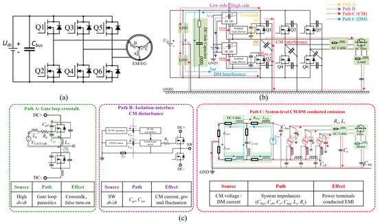
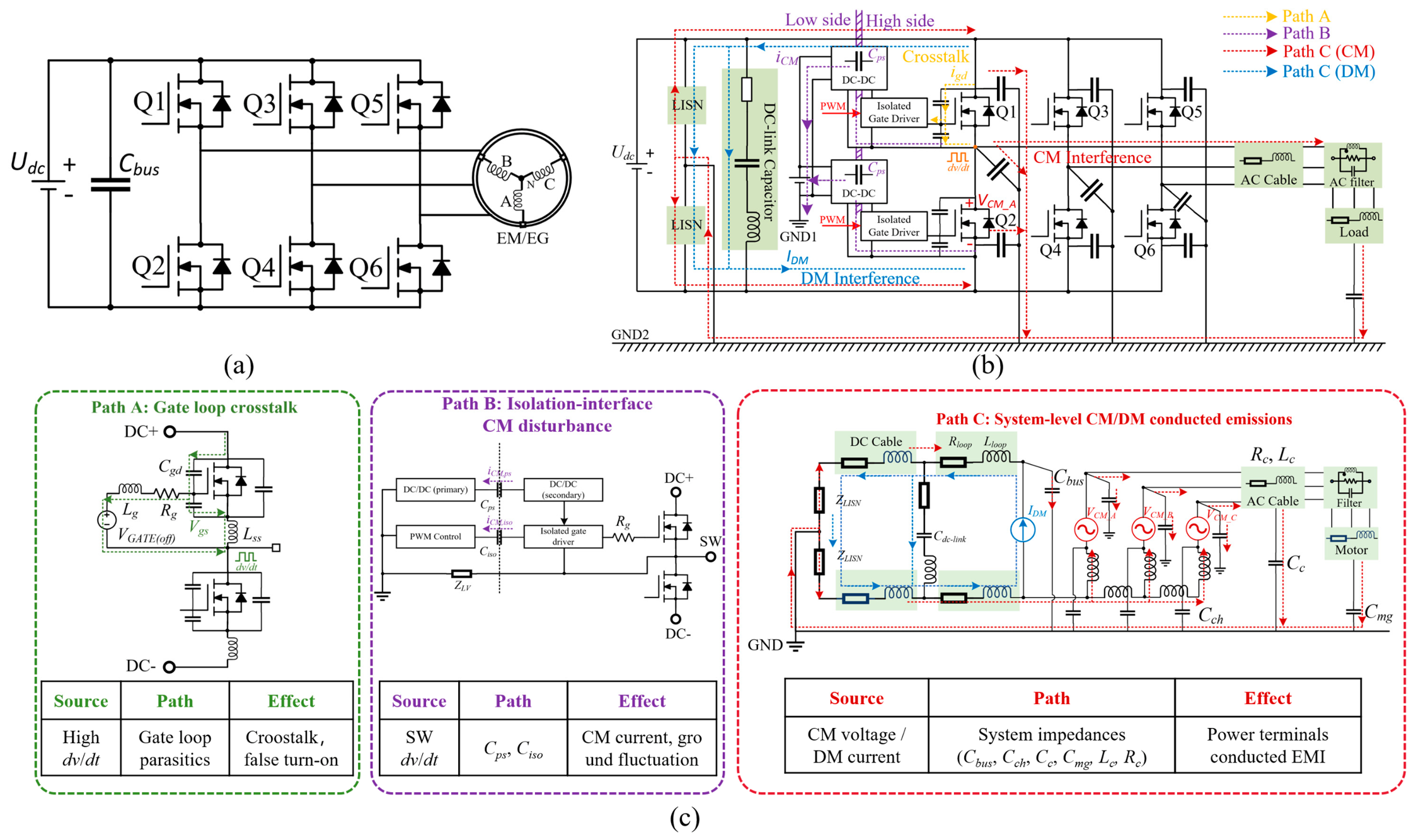
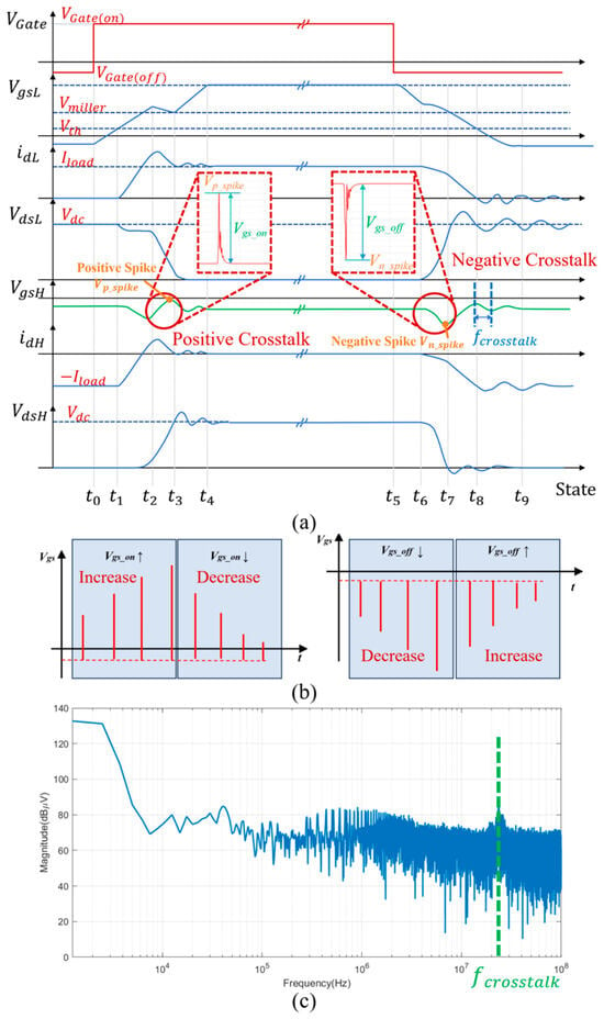
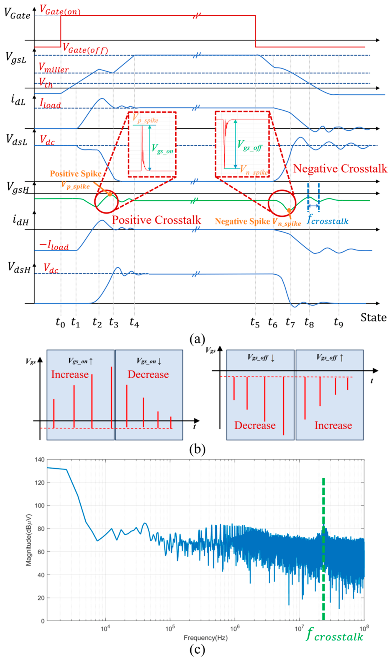
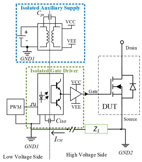
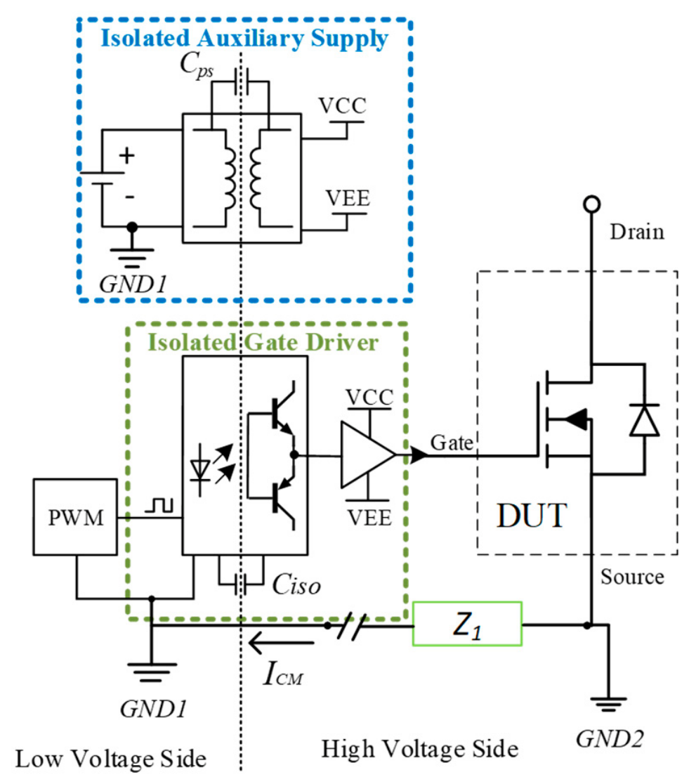
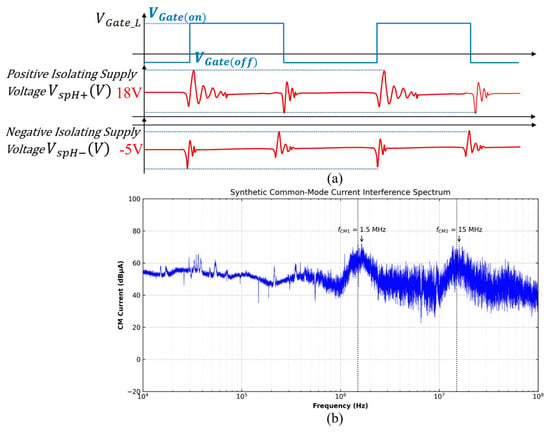
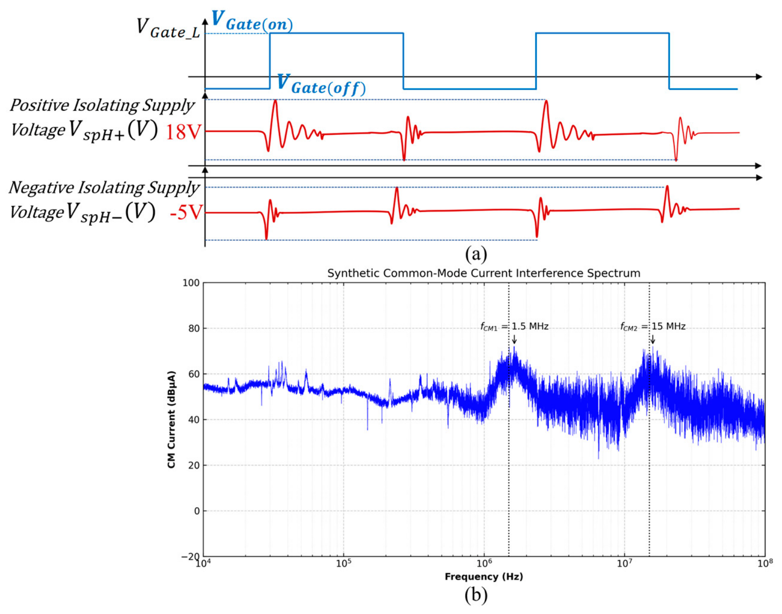
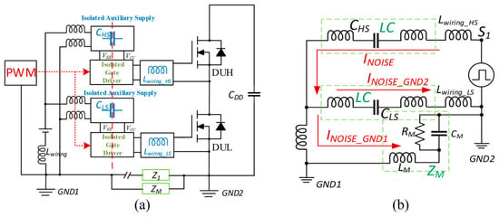
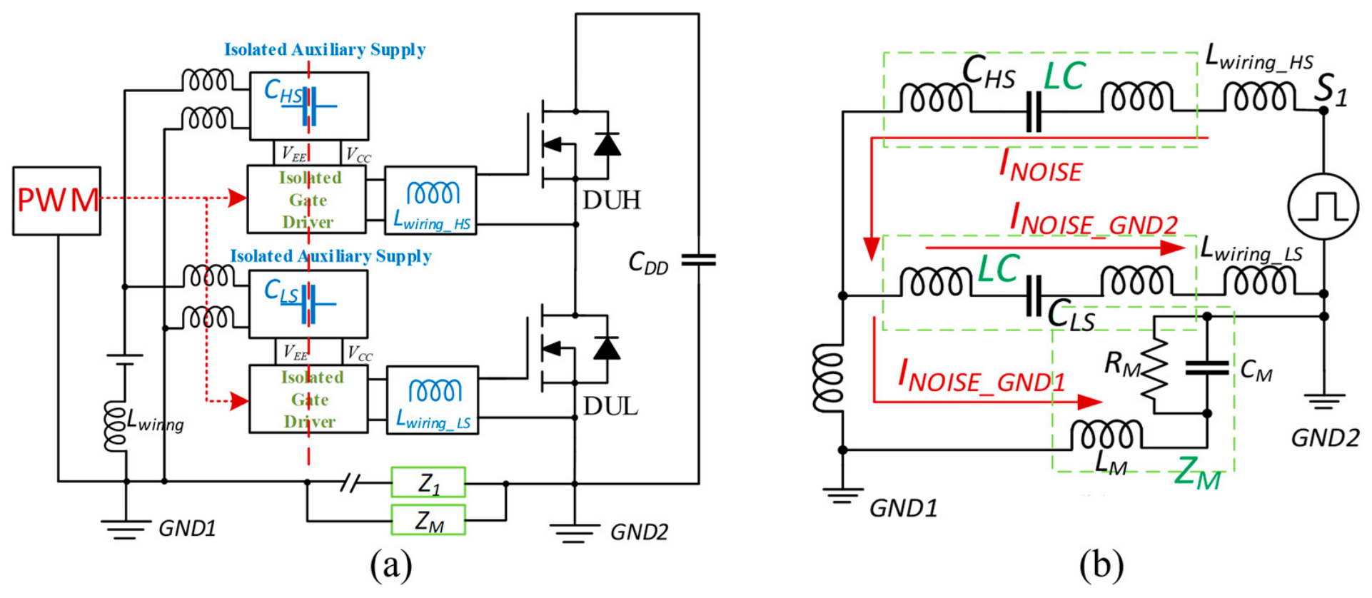
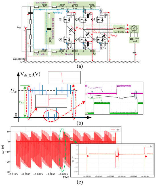
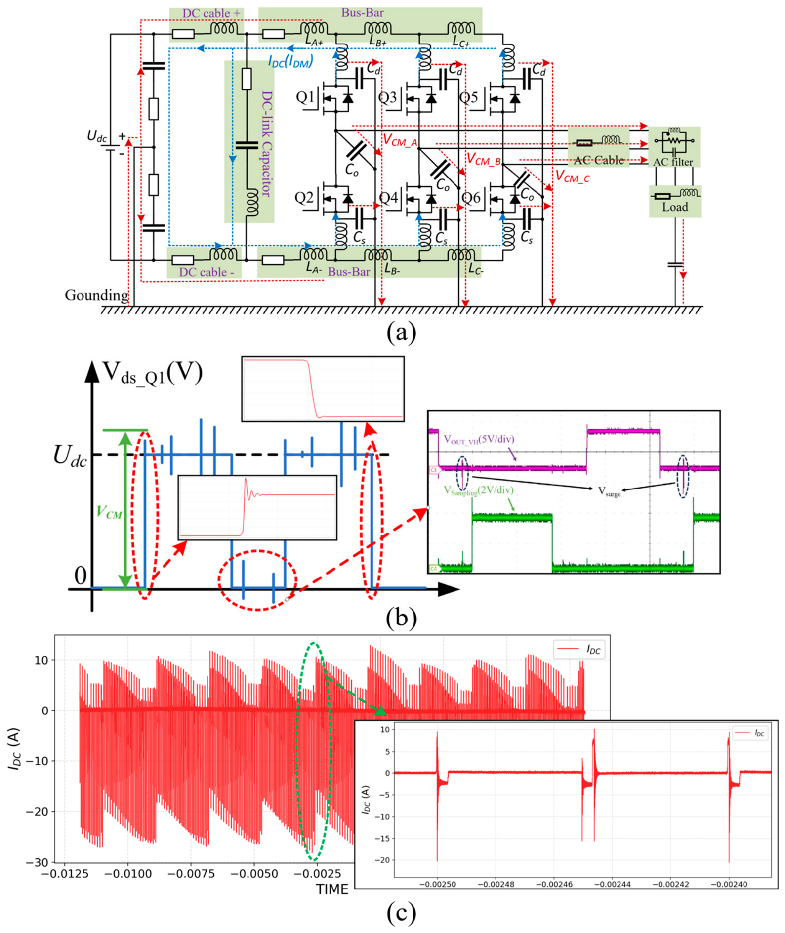
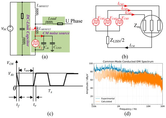
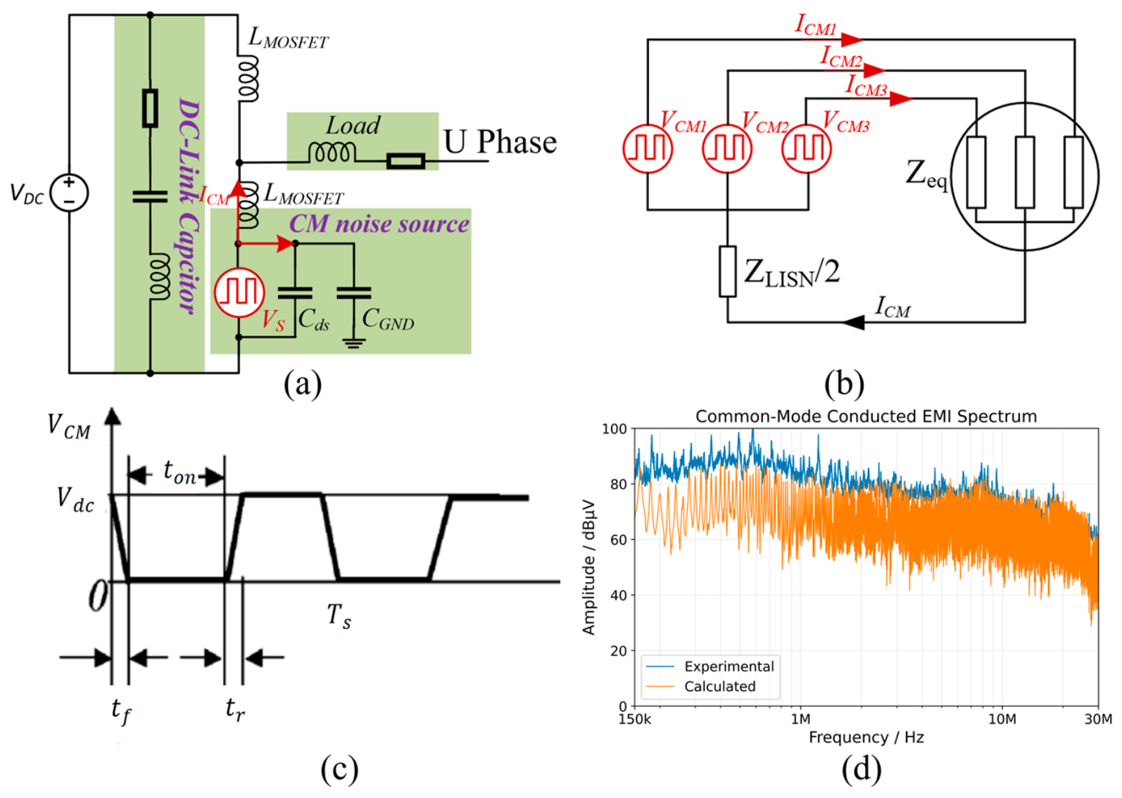
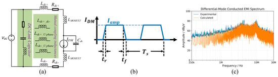
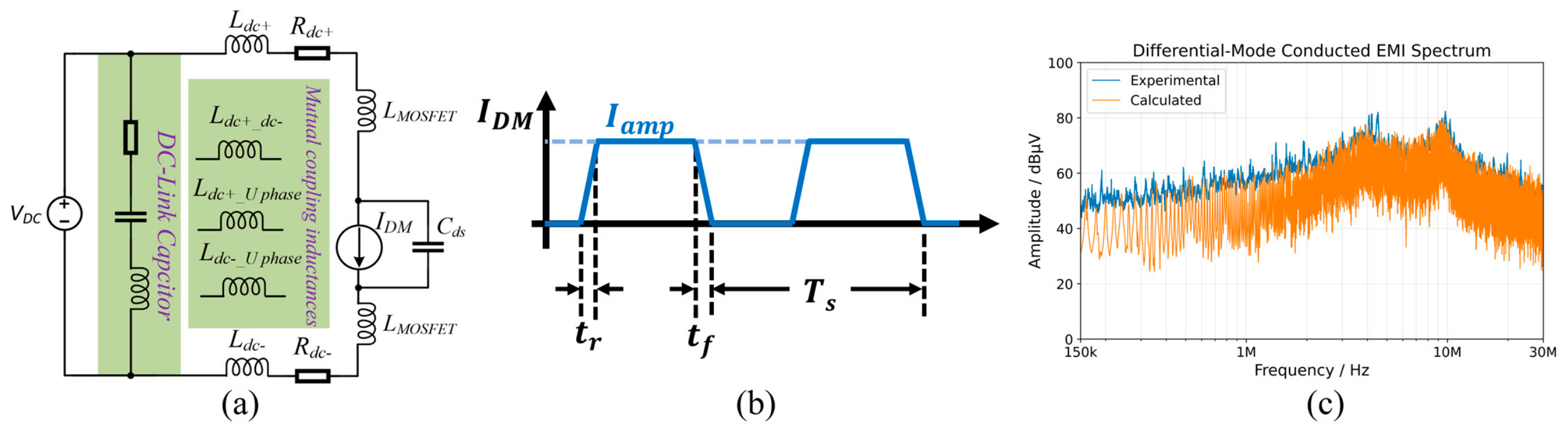
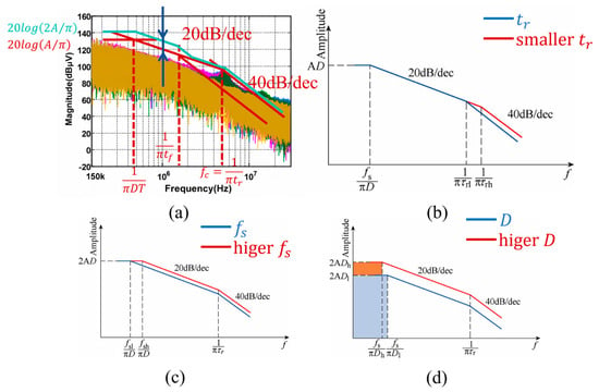
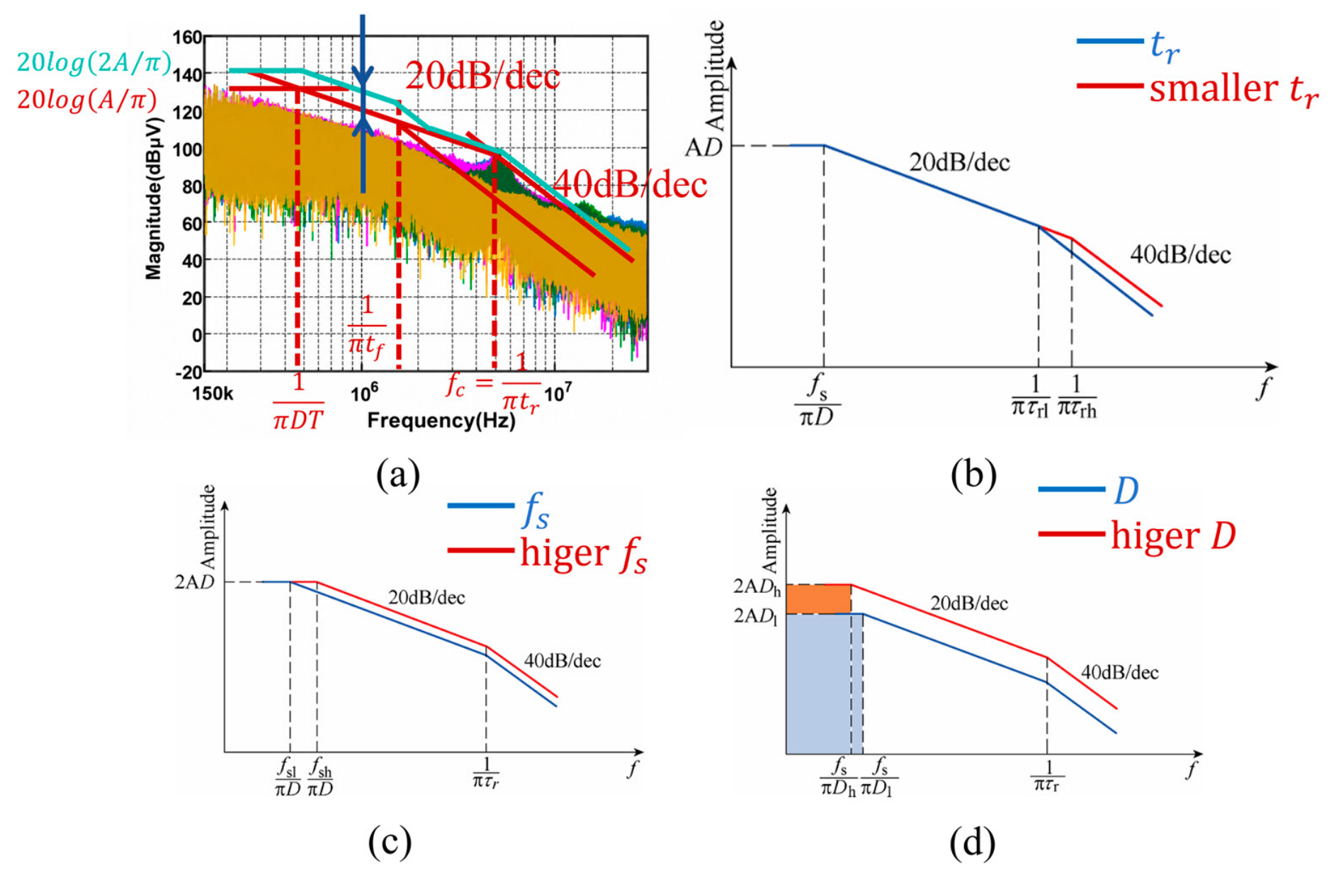
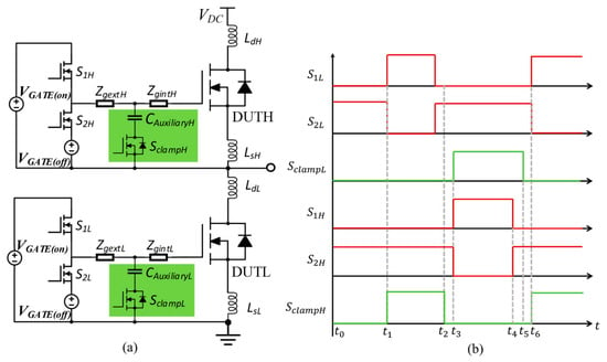
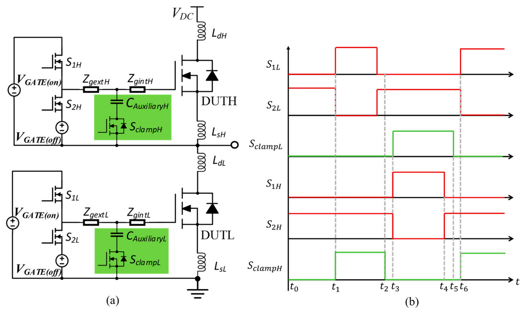
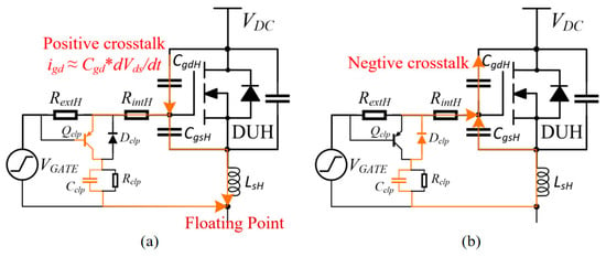
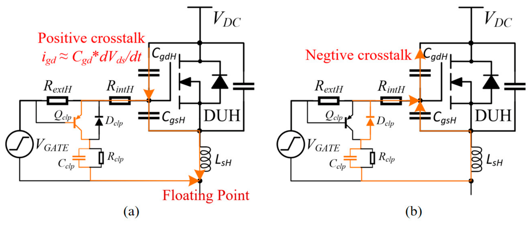
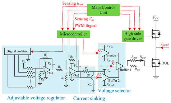
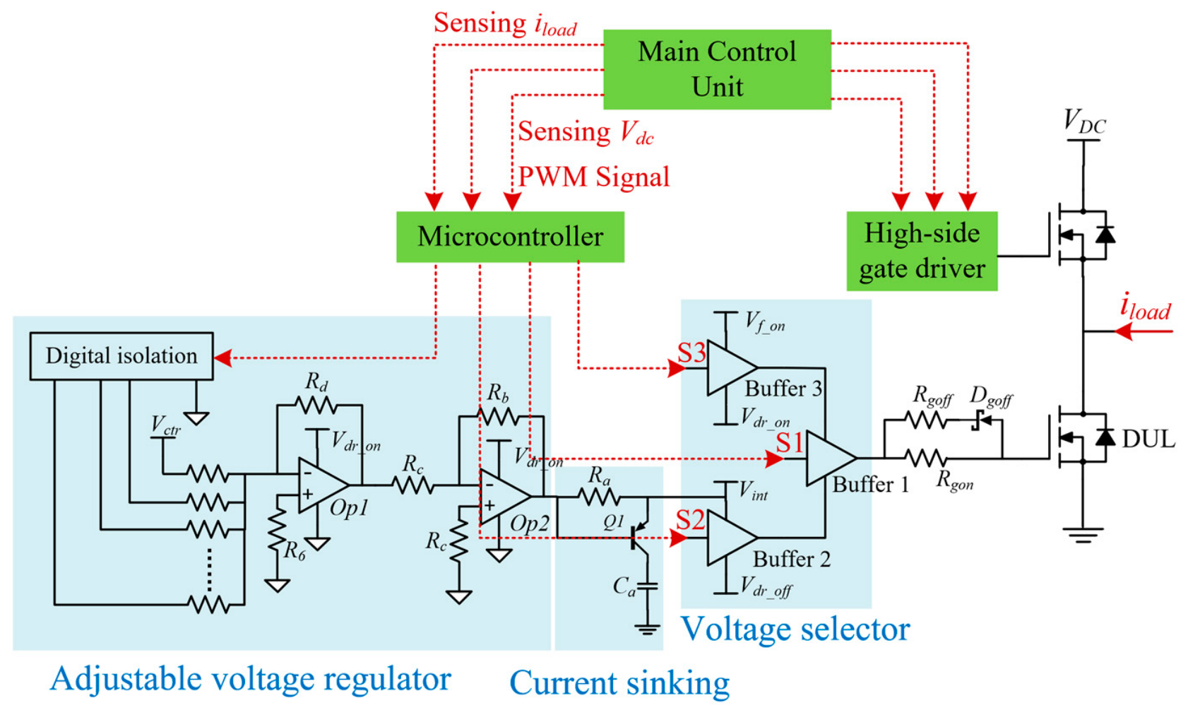
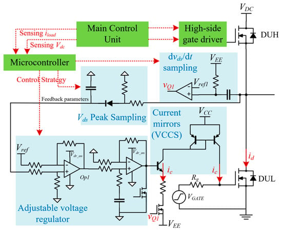
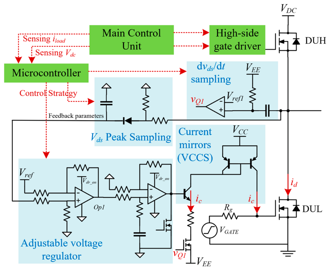
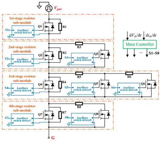
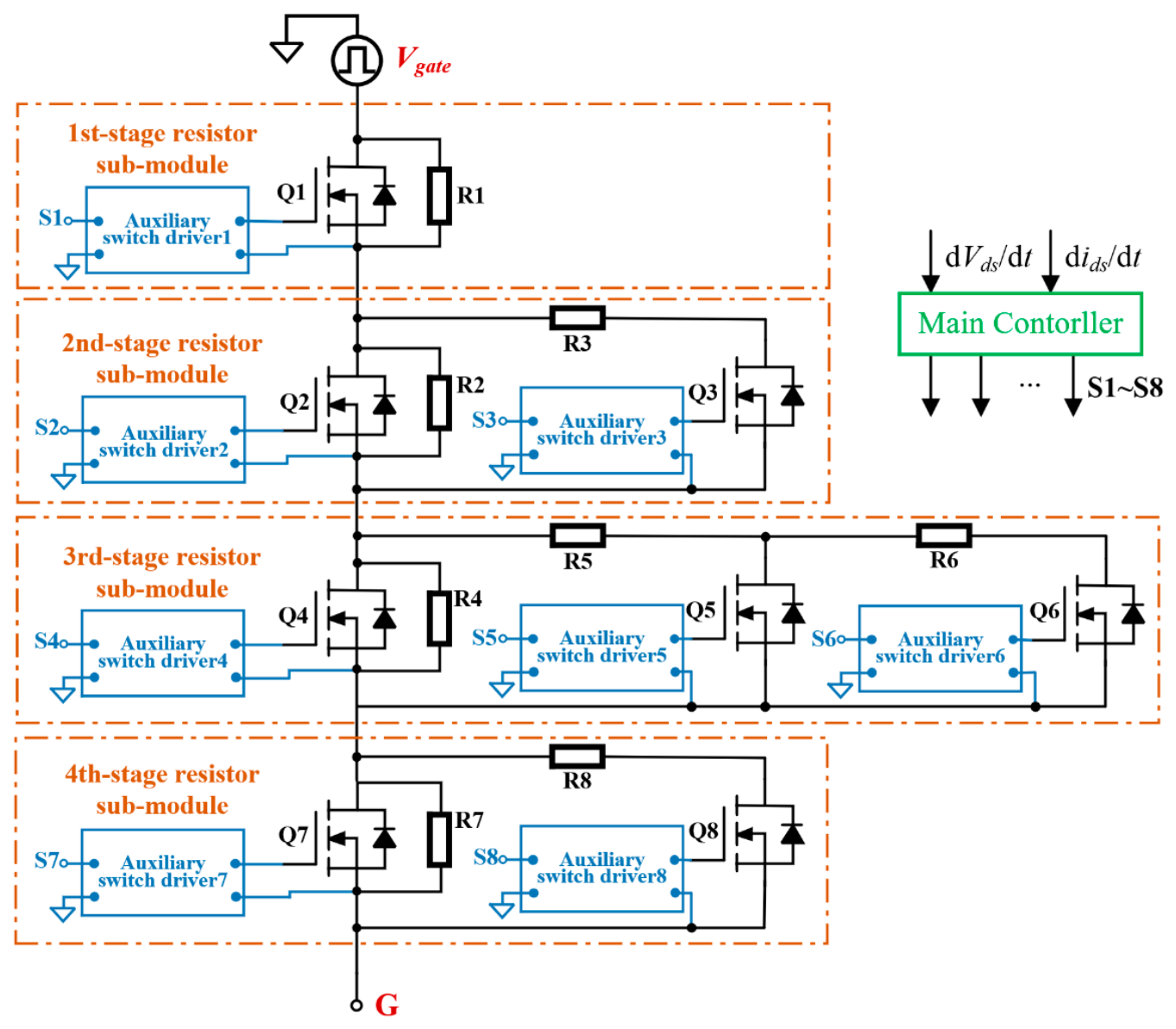
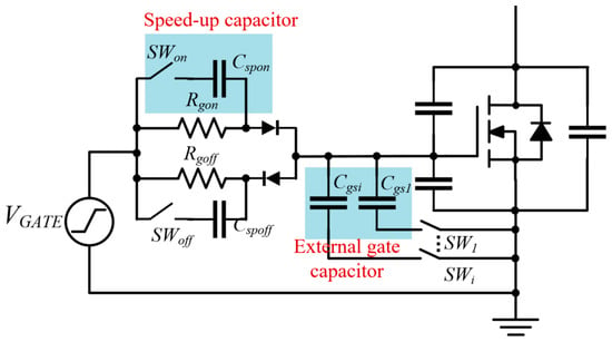
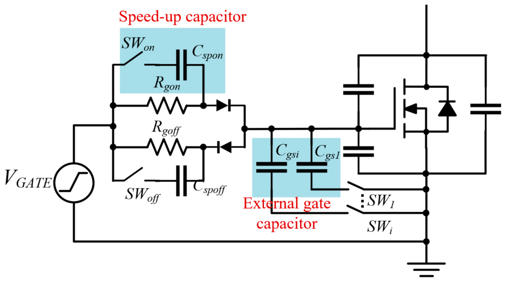
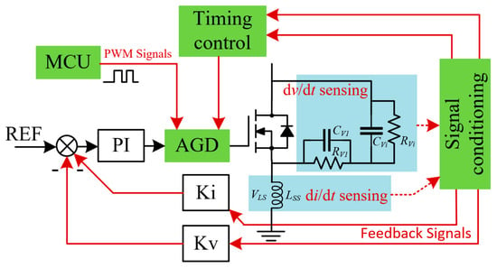
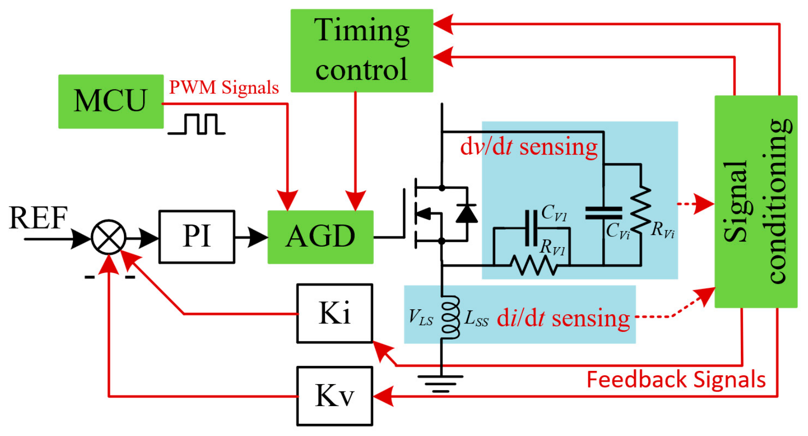
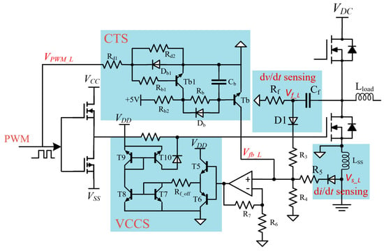
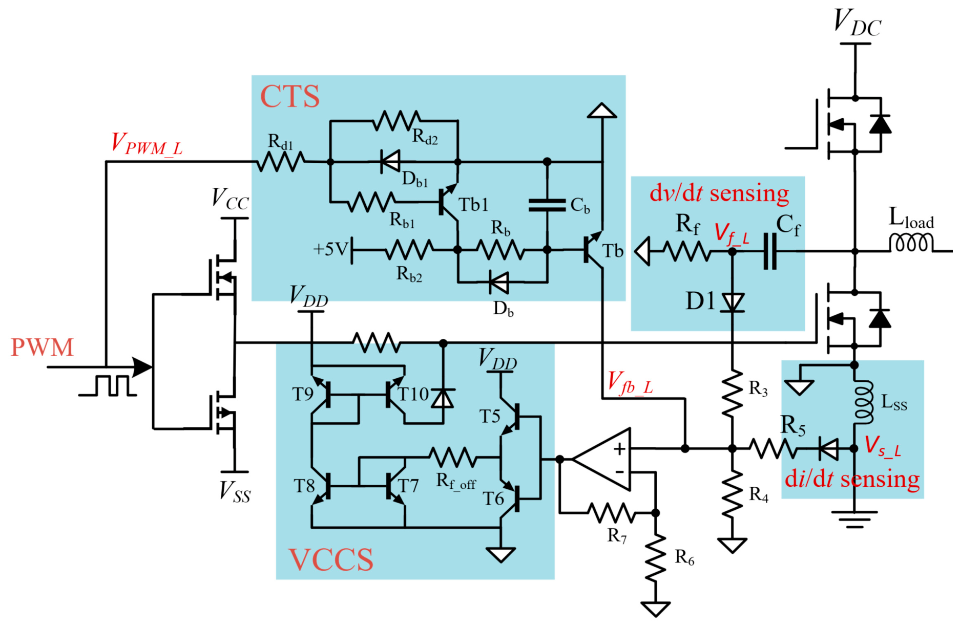
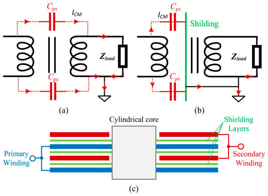
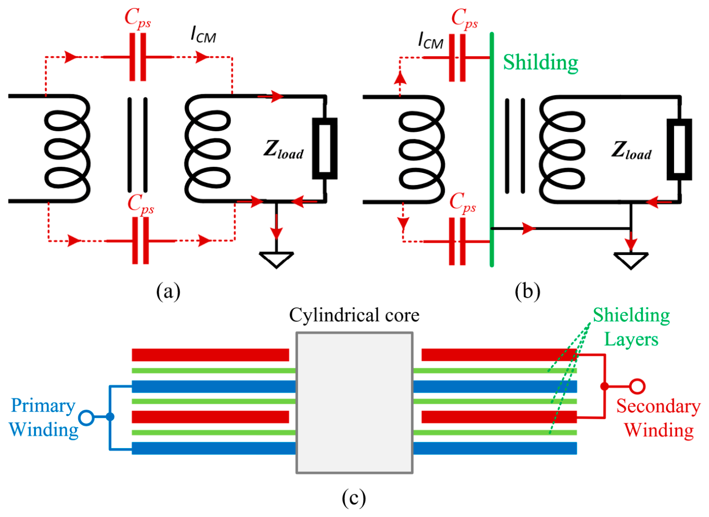
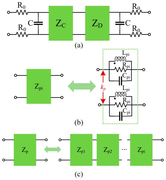
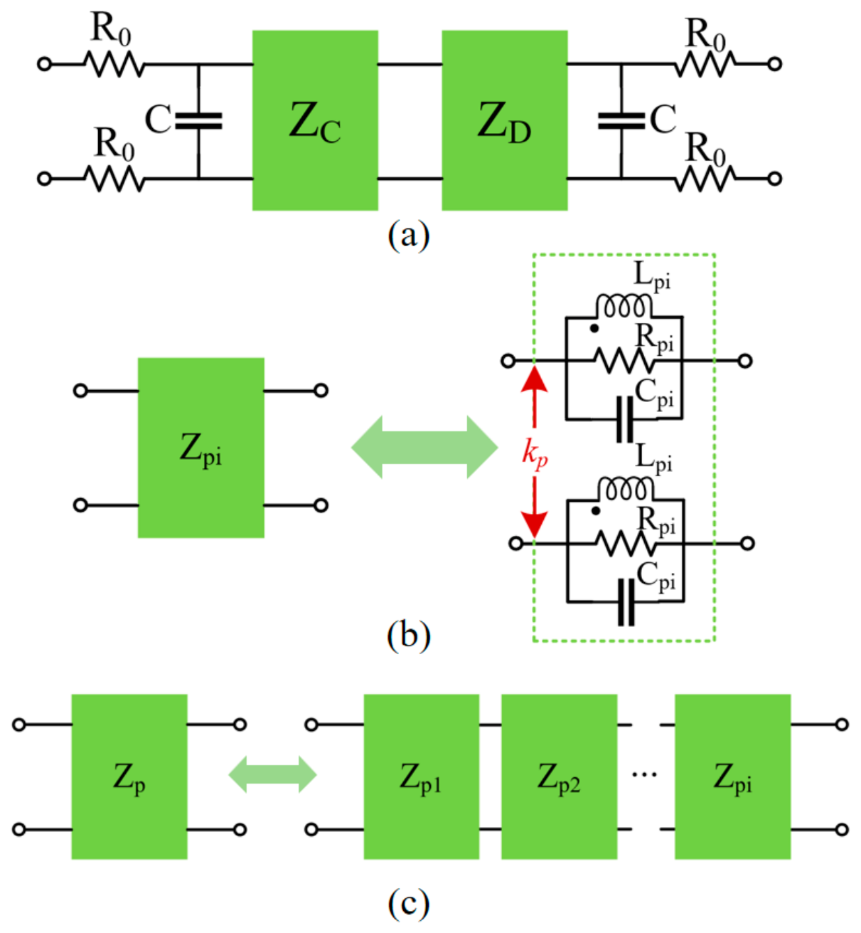
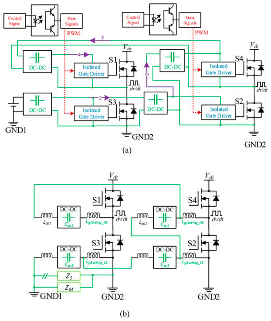
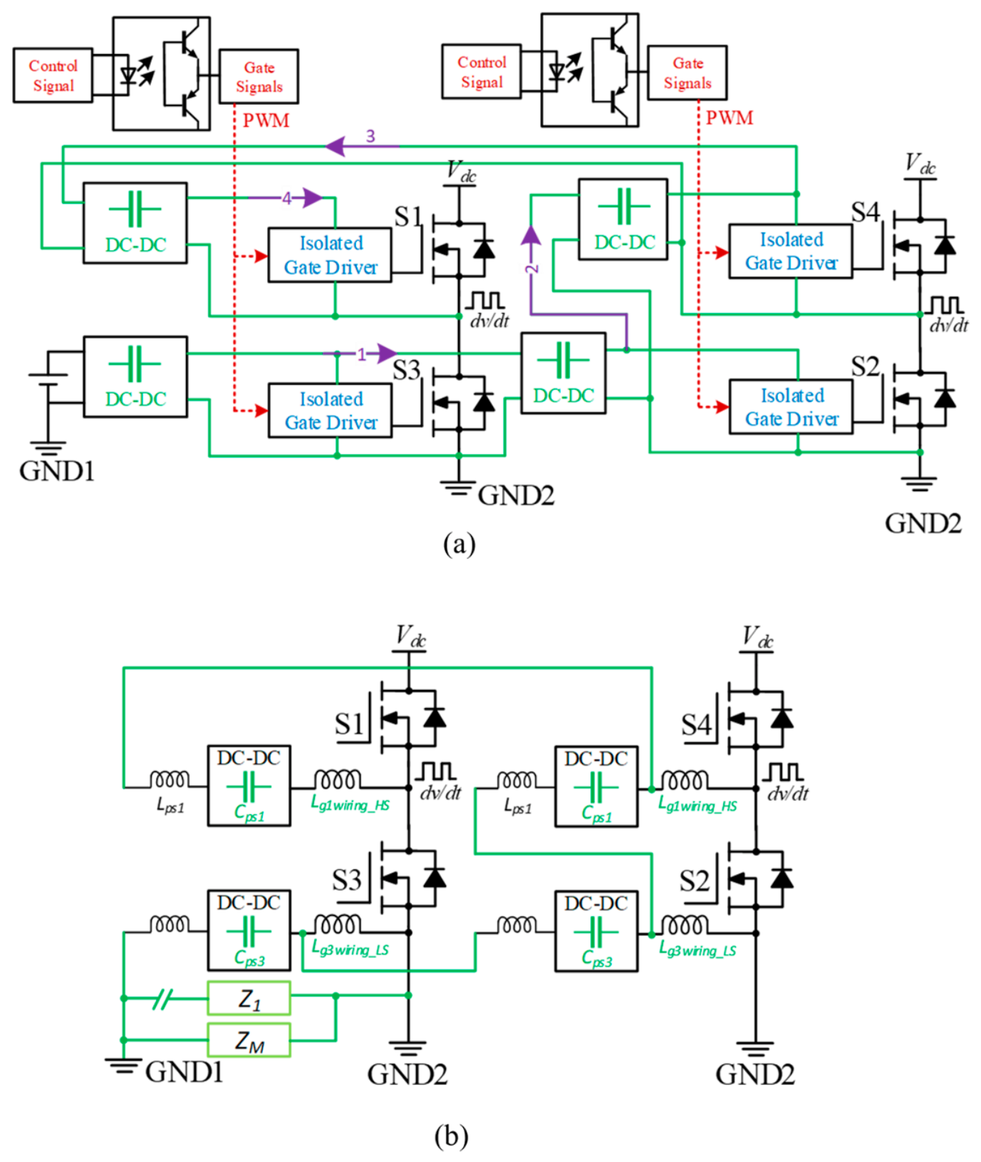
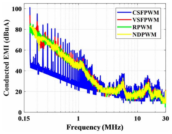
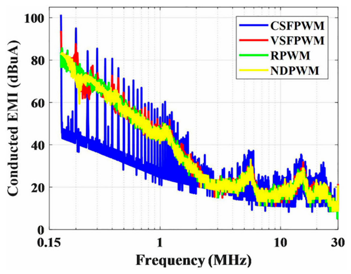
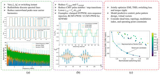
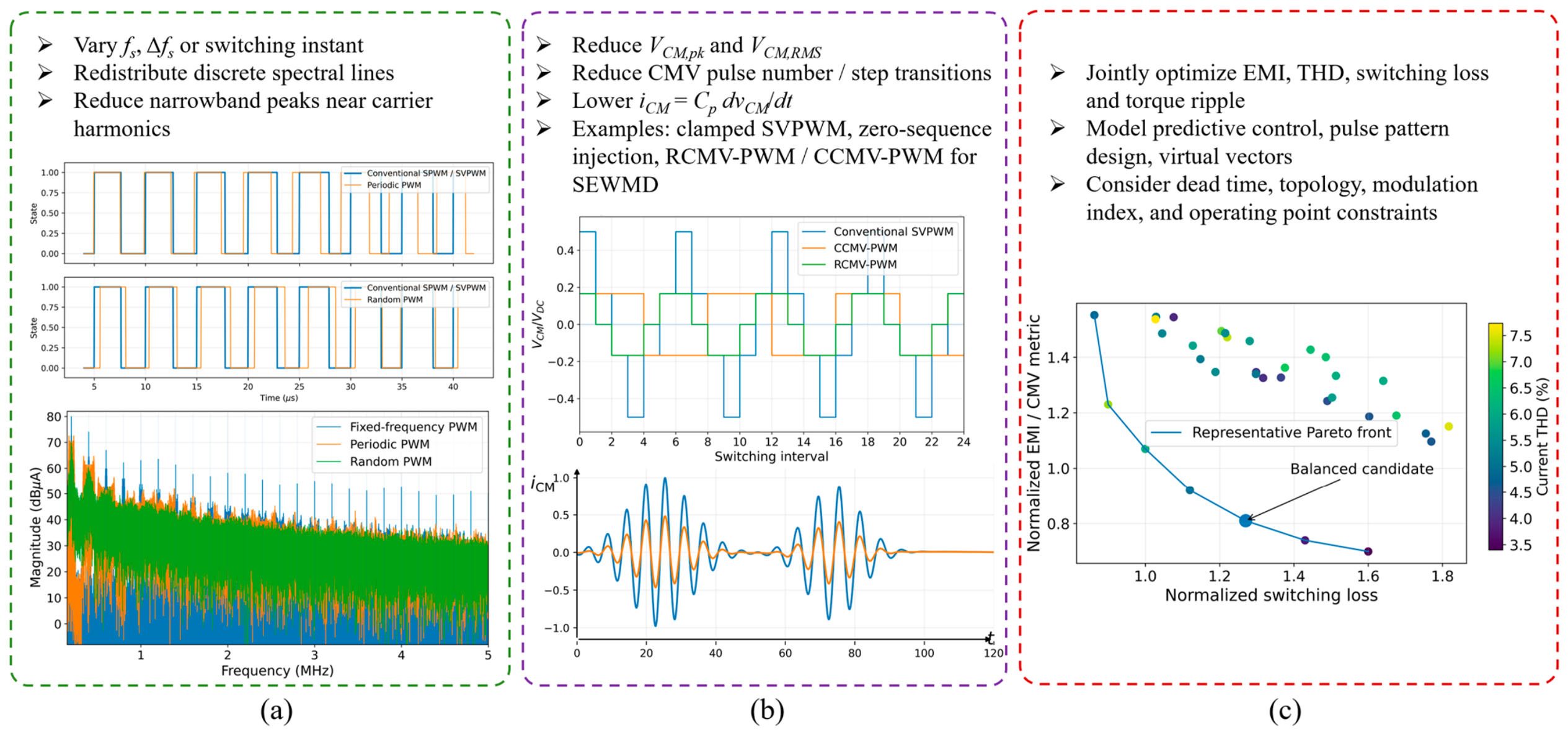
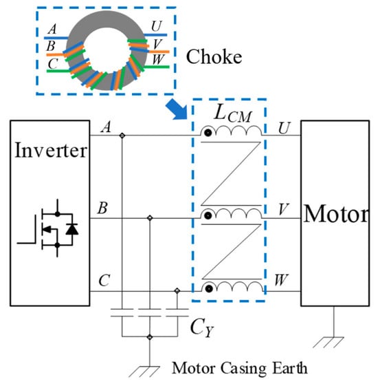
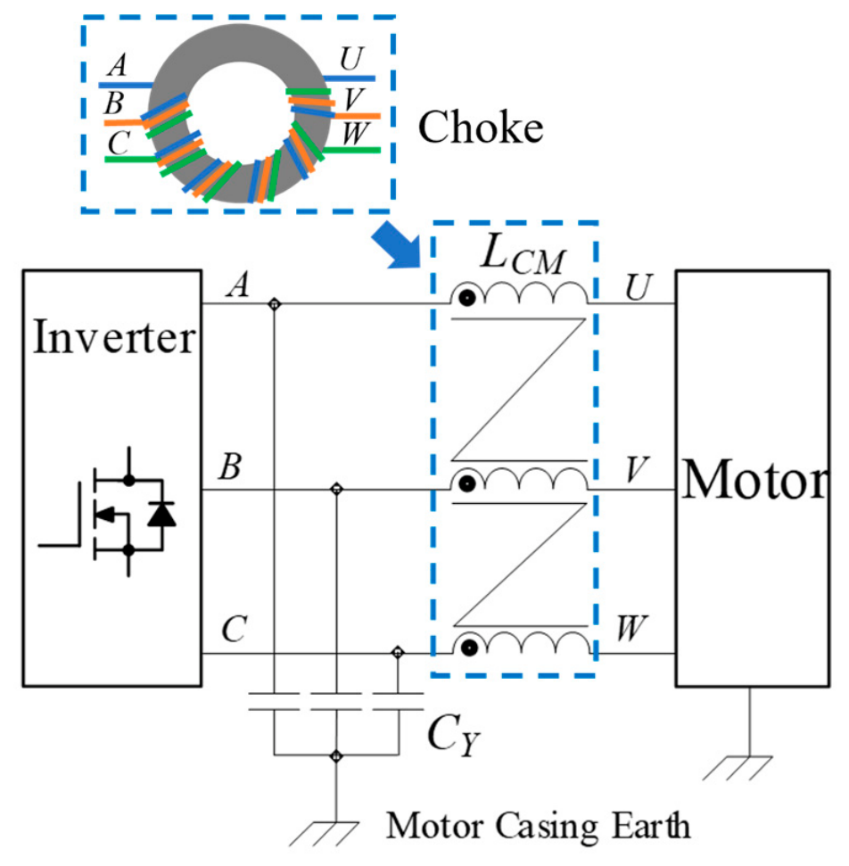

Disclaimer/Publisher’s Note: The statements, opinions and data contained in all publications are solely those of the individual author(s) and contributor(s) and not of MDPI and/or the editor(s). MDPI and/or the editor(s) disclaim responsibility for any injury to people or property resulting from any ideas, methods, instructions or products referred to in the content. |
© 2026 by the authors. Licensee MDPI, Basel, Switzerland. This article is an open access article distributed under the terms and conditions of the Creative Commons Attribution (CC BY) license.