


Abstract
In the present work, thin TiO2 films were obtained by the sol–gel spin-coating method on glass and ITO-covered glass substrates. The crystallization evolution of the thin films was studied by the X-ray Diffraction (XRD) technique. The results indicate that the films’ crystalline structure was greatly affected by substrate type. X-ray photoelectron spectroscopy (XPS) revealed the chemical states of the TiO2 films and proved the formation of TiO2 on ITO substrates. Field Emission Scanning Electron Microscopy (FESEM) showed that the TiO2 films deposited on the ITO glass possessed a uniform and homogeneous surface morphology. The influence of optical properties (transmittance, reflectance, and optical band gap) on substrate type, the number of layers and annealing temperatures was determined. Spectroscopic data confirmed high transparency of the TiO2 films obtained on ITO substrates as the transmittance in the visible spectral range was close to 85%. The obtained results reveal that thin TiO2 films on ITO substrates can be an excellent candidate for photovoltaic and optoelectronic applications.
1. Introduction
Titanium dioxide is one of the most investigated wide-band metal oxide semiconductors. TiO2 nanomaterials are widely applied in various fields, including electrooptical devices, microelectronics, gas sensors, lithium-ion batteries, energy harvesting/storage, photovoltaics, biomedicine, etc. [1].
Thin TiO2 films have pronounced potential due to their excellent chemical stability, non-toxicity, environmental friendliness and interesting electronic properties [2]. The main crystalline phases of titanium dioxide are rutile, which is the thermodynamically stable phase; brookite; and anatase. Brookite and anatase are metastable phases, but anatase is found to be more stable than brookite [3]. The anatase and rutile polymorphs have a tetragonal structure, built from TiO6 octahedra. The brookite phase shows an orthorhombic system [4].
TiO2 has also gained substantial scientific interest due to its high refractive index (2.52 and 2.70–2.76 for anatase and rutile bulk titania, respectively [5]), wide band gap (3.2 eV for anatase, 3.1 eV for brookite, and 3.0 eV for the rutile phase [6]), and high transparency in the visible and near-infrared spectral range [7]. For example, anatase TiO2 is widely known to be photocatalysts, water splitting, and self-cleaning surfaces [8]. Rutile titania has piezoelectric and ferroelectric properties, and it is applied in sensors, actuators and biosensing applications [9]. The brookite phase is reported to be attractive for gas-sensing capabilities for detecting volatile organic compounds (VOCs) and other gaseous pollutants [10].
Recently, TiO2 films as n-type semiconductors have been investigated for usage in heterojunction-based transparent photovoltaic cells. Traditional silicon-based photovoltaics are progressively enhanced in performance, but there are still a huge number of applications to be covered, such as transparent electronics and transparent photovoltaics (transparent architectural components as windows or roofs) [11]. Transparent photovoltaics (TPVs) combine high optical transparency with solar energy conversion by selectively absorbing invisible UV and/or near IR wavelengths [12]. To realize TPV cells, metal oxides like TiO2 and ZnO can be promising candidates due to their high energy band gap, which allows for the passing of visible light through them, while TPV cells absorb harmful UV light and generate electric energy [12].
One important issue for industrial applications of thin TiO2 films is the possibility for low costs, large area deposition and compatibility with different substrates [13]. TiO2 coatings have been fabricated by a huge variety of technological approaches, such as magnetron sputtering, chemical vapor deposition, atomic layer deposition, pulsed laser deposition, etc. [14]. The sol–gel method has a large number of advantages over other deposition techniques, including simplicity and cost-effectiveness. It requires relatively low processing temperatures [2]. The sol–gel process allows for effective compositional control, molecular-level homogeneity and the capability to produce homogeneous multicomponent oxide films, eliminating the need for expensive and complex equipment [2,15].
This study reports on the continuation of previous research on sol–gel TiO2 films obtained on different types of substrate–silicon wafers, glass, and ITO-covered glass. In our earlier preliminary study [16], the results of an FTIR analysis of 500 °C annealed TiO2 films on silicon and ITO substrates were reported. The optical transmittance and reflectance spectra were explored for TiO2 films deposited on glass and ITO substrates and treated at 300 and 500 °C. FESEM microscopy revealed the cross-section images of 500 °C annealed samples. The first measurements of the work function of sol–gel TiO2 films obtained on the two types of substrates, Si and ITO, were given [16]. This work presents the crystallization evolution of sol–gel TiO2 films independent of substrate type (glass and ITO), film thickness (2, 3 and 5 layers) and annealing temperature (300 and 500 °C). The FESEM technique was applied to deepen the investigation and to obtain accurate information about the surface microstructure of sol–gel TiO2 coatings deposited on glass and ITO substrates. The optical properties were analyzed by UV-VIS-NIR spectroscopy. The determined results for transparency, reflectance, optical band gap and refractive index are discussed. The work function values of TiO2 multilayered films obtained on the different substrates (Si and ITO) were established.
2. Materials and Methods
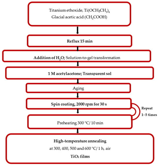
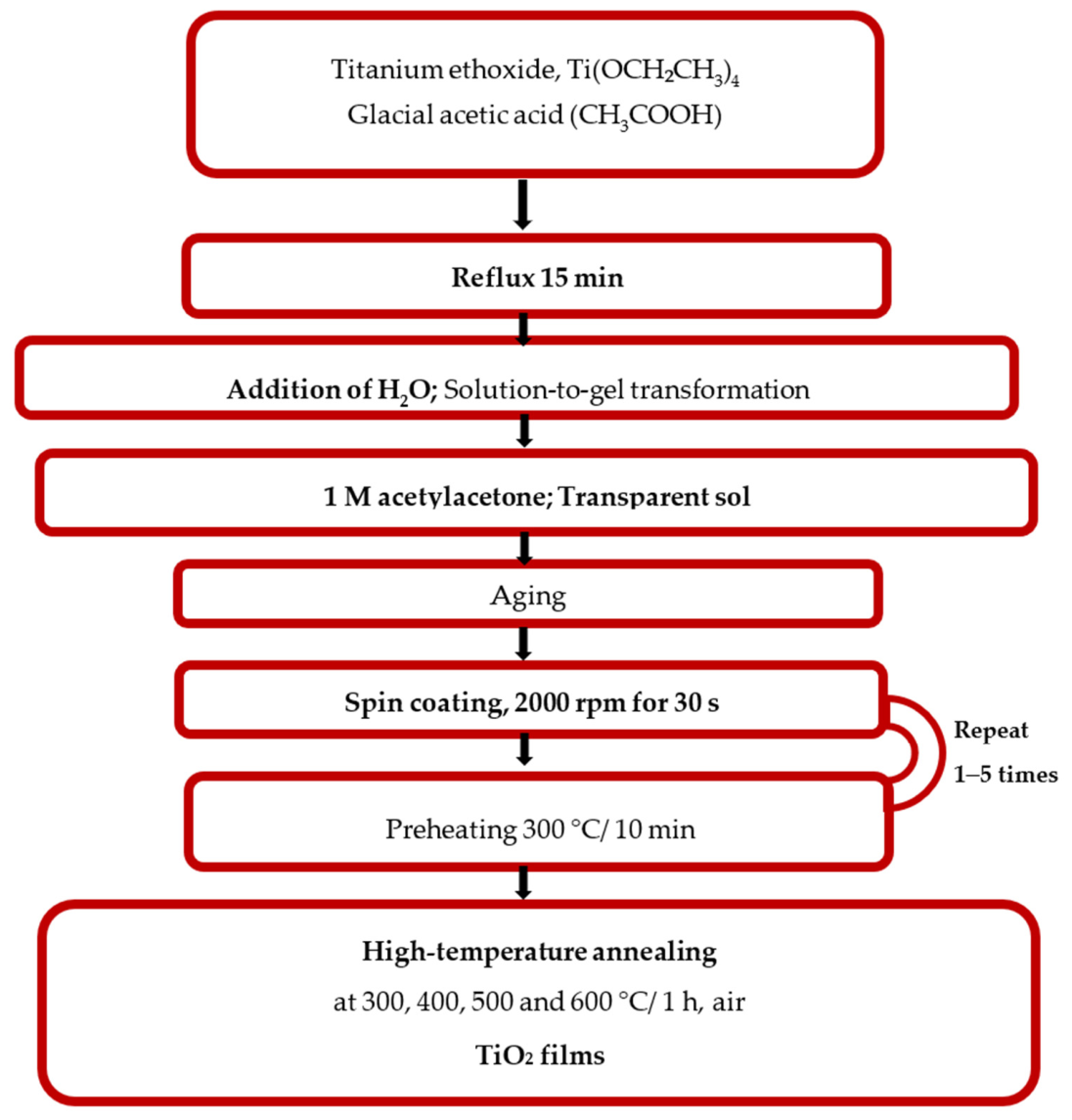
The preparation steps of the sol solution synthesis were described previously in detail [17]. Titanium ethoxide, Ti(OCH2CH3)4 ((>97% purity, Fluka Chemie, Buchs, Germany), was chosen as a precursor. After adding 1.5 M of glacial acetic acid (CH3COOH) (100%, Merck KgaA, Darmstadt, Germany), an acetate modification occurred. Hydrolysis, condensation reactions and transformation of the solution to a gel were caused by introducing a certain amount of water. The transformation of the gel to a transparent sol appeared after the addition of 1 M of acetylacetone (>98%, Sigma Aldrich Chemie, Buchs, Germany), acting as a bidentate chelating ligand and a stabilizer. The sol–gel process flow chart is presented in Figure 1. The synthesized sol solution achieved more than 12 months of stability without losing its excellent film-forming properties.
Figure 1.
Schematic diagram of the sol–gel spin-coating deposition of thin TiO2 multilayered films.
For this study, three types of substrates were used: soda–lime glass (25 × 25 mm), ITO (indium tin oxide-coated glass, sheet resistance <15 Ω/sq., 1.1 mm thick, 25 × 25 mm, unpatterned, Ossila Ltd., Sheffield, UK) and Si wafers ((FZ, p-type, <100>, resistivity 4.5–7.5 Ω). The films were obtained by spin coating (using a P 6708 spin coater, PI-KEM Limited, Staffordshire, UK) at 2000 rpm for 30 s. The preheating temperature was 300 °C for 10 min (the preheating temperature is an initial heating step applied between layers and before the final annealing). The sequence of the spin-coating and preheating procedure was repeated to achieve TiO2 films with 1, 2, 3 and 5 layers. The deposited films were subjected to high-temperature treatments using a chamber furnace (Tokmet TK Ltd., Varna, Bulgaria). The heating and cooling rates were adjusted at 10 °C/min. The annealing temperature ranged from 300 to 500 °C for a duration of 60 min in ambient air.
The structural properties of the sol–gel titanium dioxide films were characterized by XRD analysis with the help of a Bruker D8 Advanced diffractometer (Bruker Cooperation, Karlsruhe, Germany) with monochromatic CuKα radiation in the Bragg–Brentano reflection geometry. The measurements were performed in the 2θ range from 35 to 90° with a constant rate of 0.02 s−1. The X-ray wavelength was 1.5406 Å.
An XPS study of TiO2 films was performed by using a Kratos AXIS Supra spectrometer (Kratos Analytical, Manchester, UK) with an achromatic Al X-ray source under the vacuum that was better than 10−8 Pa at a 90-degree take-off angle. Each analysis started with a survey scan from 0 to 1200 eV and a pass energy of 160 eV at steps of 0.5 eV with 1 sweep. For a high-resolution analysis the number of sweeps was increased, and the pass energy was lowered to 20 eV at steps of 100 meV. The C 1s photoelectron line at 284.6 eV was used for calibration of recorded spectra. The survey spectra and the high-resolution spectra of carbon, oxygen, and titanium were analyzed.
FESEM observations were done using a Zeiss Supra 40 Field Emission Scanning Electron Microscope (Carl Zeiss AG, Oberkochen, Germany). Cross-section samples were prepared by focused ion beam etching using FEI’s Helios NanoLab DualBeam system (FEI Company (Thermo Fisher Scientific, Inc.), Hillsboro, OR, USA). The cross-section images were used for film-thickness determination. It was found that the two-layered film was 200 nm thick, independent of annealing temperatures. The thickness of the three- and the five-layered TiO2 films was 300 and 500 nm, respectively.
Optical characterization was performed with the UV–VIS–NIR Shimadzu 3600 double-beam spectrophotometer (Shimadzu Corporation, Kyoto, Japan) in the spectral region of 240–1800 nm. The transmittance spectra were taken against air. The reflectance spectra were measured by using the specular reflectance attachment (5° incidence angle) and Al-coated mirror as a reference.
The Work function (WF) of the samples was determined with the help of a Scanning Kelvin Probe (SKP5050, KP Technology Ltd., Wick, UK). A Kelvin probe measures the contact potential difference between a sample and tip. The WF of the sample is calculated by determining the WF of the tip calibrated against a known surface.
3. Results and Discussion
3.1. XRD Investigation
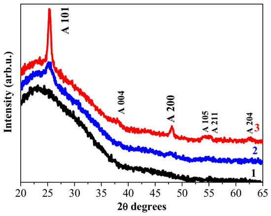
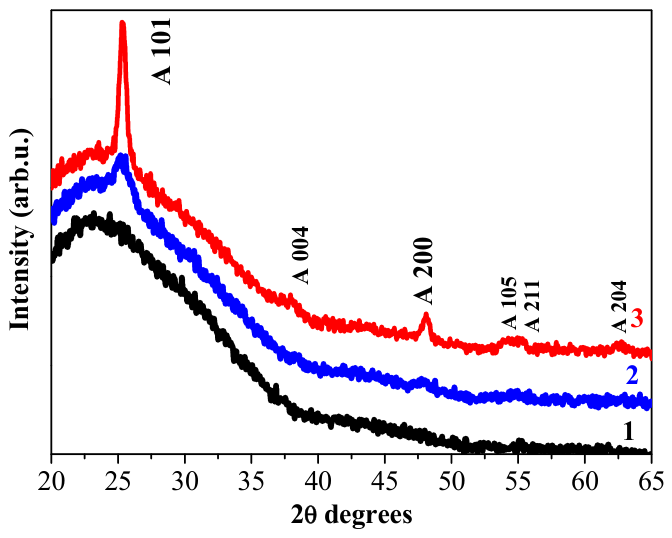
The crystalline structure of the sol–gel-derived TiO2 films was studied by the XRD technique. The impact of substrate type and film thickness on film crystallization was analyzed. Figure 2 shows the XRD patterns of the TiO2 coatings obtained on the glass substrate. The studied films comprised three and five layers. From the presented XRD pattern (Figure 2, curve 1), it can be seen that the three-layered sample annealed at 300 °C revealed no clear XRD lines, and there is the appearance of a broad “hump” or an amorphous halo. This is an indication for an amorphous-like structure. It is known that very tiny crystallite sizes might not be observed in diffraction patterns, as they are below XRD detection limits [18].
Figure 2.
XRD patterns of sol–gel TiO2 films obtained on the glass substrate, where (1) represents the pattern of TiO2 films with three layers (black color) annealed at 300 °C, (2) five-layered films annealed at 300 °C (blue color) and (3) five-layered films treated at 500 °C (red color). The letter A marks the anatase phase.
Increasing the number of layers, the TiO2 films with five layers (Figure 2, curve 2) exhibits the beginning of film crystallization after low-temperature annealing at 300 °C. A clear line at 25.19 degrees over the halo is detected, and this is consistent with the standard database reference (PDF card 00-021-1272) of the anatase TiO2 phase. The (101) reflection plane is the most intense and characteristic XRD peak for the anatase phase of titanium dioxide. Another indication for the start of film crystallization is the appearance of the broad and weak line at 2θ ≈ 48°, corresponding to the anatase (200) plane.
Annealing at the highest temperature of 500 °C resulted in the presence of six XRD lines, as can be observed in the XRD pattern of the five-layered TiO2 film (Figure 2, curve 3). All the diffraction peaks are assigned to the anatase phase (PDF card 00-021-1272), and the formation of the pure anatase crystal phase is confirmed. No characteristic peaks for other TiO2 polymorphs are detected in the XRD patterns (Figure 2).
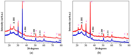
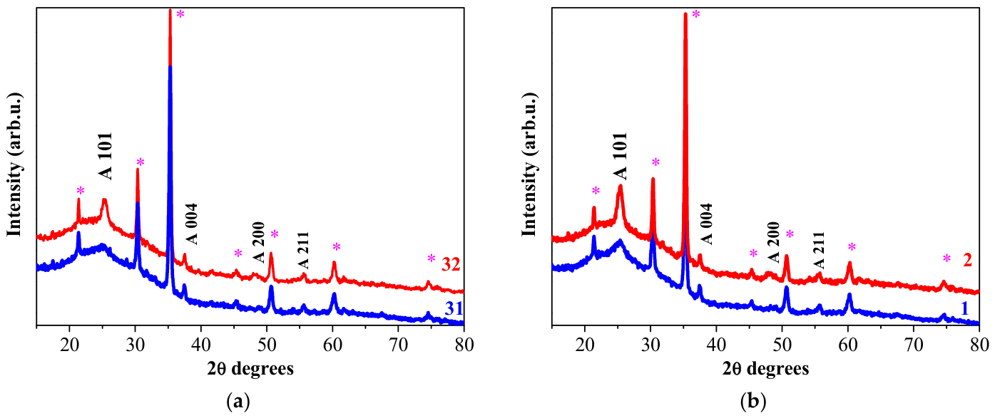
Figure 3 illustrates the XRD patterns of the TiO2 films deposited on ITO substrates with three and five layers and additionally annealed at 300 and 500 °C. The three-layered sample treated at 300 °C possesses a polycrystalline structure as three XRD lines can be clearly seen (see Figure 3a, curve 31, blue color), excluding reflections due to SnO2 (ITO substrates). These three signals are attributed to the (101), (004), and (200) crystal planes of anatase TiO2, respectively.
Figure 3.
XRD patterns of (a) three-layered TiO2 films obtained on the ITO-covered glass substrate, where 31 marks the sample after annealing at 300 °C and 32—at 500 °C, and (b) five-layered TiO2 films obtained on ITO substrates after annealing at 1—300 °C and 2—500 °C. The letter A marks the anatase phase, and the asterisk symbol (*) exhibits XRD lines due to SnO2 (ITO coating) (PDF 01-083-3350).
Increasing the annealing temperature up to 500 °C provokes an improvement in film crystallization (Figure 3a, 32, red color) as the XRD peaks become sharper and stronger. The thickest sol–gel films with five layers (Figure 3b) are also crystallized in the anatase phase as their diffraction patterns exhibit XRD reflections corresponding to the standard PDF card 00-021-1272. No lines due to the rutile or to the brookite phase are found. Crystallization is enhanced with an increase in annealing temperature, and crystallite growth is promoted.
The crystallite size for the 101 diffraction line from the XRD pattern can be determined by using the Debye–Scherrer equation [19]:
where D is the calculated crystallite size (nm); k is the shape factor, equal to 0.9; λ is the X-ray wavelength (CuKα radiation, λ = 0.15406 nm); and β is the estimated value of the full width at half maximum (FWHM). The FWHM values, the peak position and the crystallite size calculated from the XRD data are presented in Table 1. A higher annealing temperature induces larger, well-defined crystalline grains. It is worth mentioning that the five-layered TiO2 film on the glass substrate possesses the greatest crystallites, which are almost twice as great as the corresponding crystallite sizes of the TiO2 films obtained on ITO substrates. A glass substrate has a smoother and amorphous surface, which can provide fewer heterogeneous nucleation sites compared to the crystalline and rougher surface of ITO-coated glass. This suggests that the annealing of sol–gel TiO2 films on a glass substrate can trigger large crystallites rather than forming smaller grains. Another interesting observation is that the size of the crystallites of the TiO2 films grown on ITO substrates is independent of the number of layers (three and five) as they manifest very close values of the determined crystallite sizes after 500 °C annealing (see Table 1).
Table 1.
Structure parameters (position of A (101); FWHM; and crystallite size, D) and dislocation density of thin TiO2 films deposited on glass and ITO substrates.
Dislocation density, δ, is also calculated using the determined crystalline size, D (Equation (2)) [19]:
Dislocation density is a crucial parameter that indicates defects, lattice strain, and structural perfection [20]. Larger crystallites induce lower dislocation density values. For TiO2 films on ITO substrates, increasing the annealing temperature leads to a decrease in dislocation density, which supposes better lattice ordering.
The film structure and crystallite sizes reflect optical behavior. Greater crystallite sizes provoke a rougher film morphology, which influences film transparency, reflectance and light scattering. It is also known that crystallite sizes can change the optical band gap [21]. XRD research has found that substrate type affects film crystallizations and the sizes of the formed crystallites. An ITO substrate provokes the beginning of crystallization at lower temperatures for sol–gel TiO2 films despite the number of layers. The three- and the five-layered films on glass substrates show a mainly amorphous structure after annealing at 300 °C, as the thickest film (5 layers) reveals very broad diffractions, corresponding to peaks (101) and (004) (anatase phase). There are no rutile or brookite characteristic diffraction peaks detected. The XRD study revealed that nanocrystalline anatase TiO2 films on ITO substrates can be formed after thermal annealing at and above 300 °C.
3.2. XPS Study
The XPS characterization technique was applied for obtaining information on chemical bonding and oxidation states in the thin sol–gel TiO2 films. The studied samples were the five-layered films obtained on the ITO substrate after annealing at 500 °C.
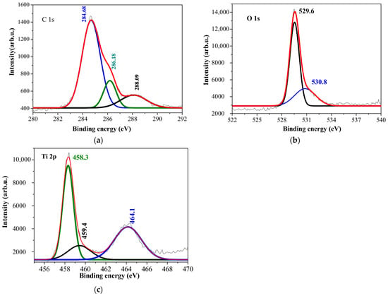
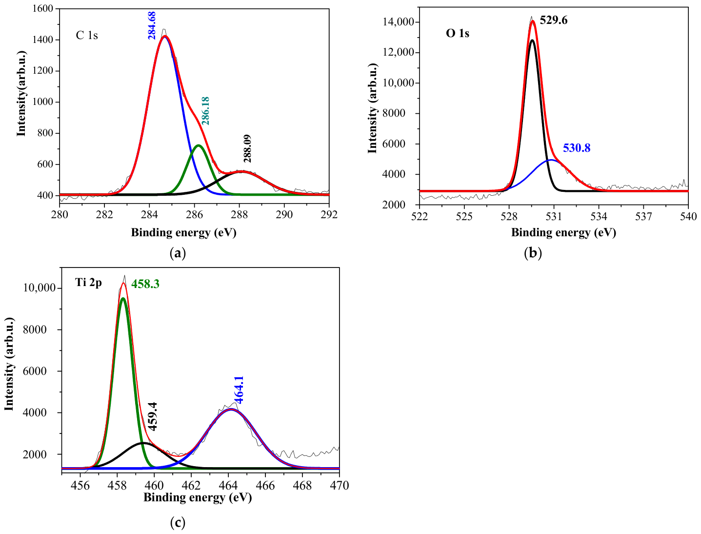
The occurrence of the C 1s peak can be attributed either to residual carbon species due to the sol–gel process or to adventitious carbon as the samples were exposed to air before XPS measurements. Sol–gel technology uses metal–organic precursors (metal alkoxides), and residual organic groups can leave behind carbon species (such as C-C, C-H, or C-O bonds) even after high-temperature annealing procedures. The deconvolution of the C 1s spectrum (Figure 4a) displays three distinct peaks. The dominant peak at 284.68 eV is due to C-C and C-H bonds (hydrocarbon), and it is assigned to adventitious carbon. The other peak at 286.18 eV is attributed to carbon–oxygen-bond (C-O, -C-O-C-, or -C-OH)-containing species. The 288.09 eV peak is related to O=C-O bonds or to C=O [22].
Figure 4.
High-resolution XPS spectra of (a) C 1s, (b) O 1s and (c) Ti 2p of the five-layered TiO2 films deposited on ITO-covered glass and annealed at 500 °C.
The asymmetric shape of the O 1s spectrum makes two distinct contributions: at the binding energies of 529.6 eV and 530.8 eV (Figure 4b). The O 1s peak at 529.6 eV is assigned to lattice oxygen (O2−) in the TiO2 crystal structure, and it is related to oxygen atoms bonded to Ti4+ in stoichiometric titanium dioxide. The second peak at 530.8 eV may be related to the oxygen-deficient environment or defect-associated oxygen species: oxygen bonded to Ti3+ states and/or to surface-absorbed hydroxyl groups and chemisorbed oxygen [23,24,25]. It must be noted that other researchers attribute this signal to the adventitious hydroxyls of water that are inevitably adsorbed on oxide film surfaces [26]. Further analysis is needed. Figure 4c reveals the deconvolution of the Ti 2p core-level spectrum. The doublet Ti 2p3/2 (binding energy 458.3 eV) and Ti 2p1/2 (464.1 eV) arises from spin–orbit splitting. The binding energy separation of this doublet is 5.8 eV. These peaks are consistent with Ti4+ in TiO2 lattice [27] or to the contribution of oxide–hydroxide phases of titanium [28]. It is also suggested that the binding energy of Ti 2p3/2 at 459.43 eV, together with the binding energy of O 1 s as 530.8 eV, can be connected to the formation of titanium dioxide [29]. Further investigation is needed to fully reveal the oxidation states of titanium elements in sol–gel TiO2 films. It should be noted that a previous FTIR study [16] showed the presence of residual C-H and hydroxyl groups for sol–gel TiO2 films annealed at 500 °C and deposited on ITO substrates. XPS analysis confirms the formation of titanium dioxide on ITO substrates.
3.3. FESEM Characterization
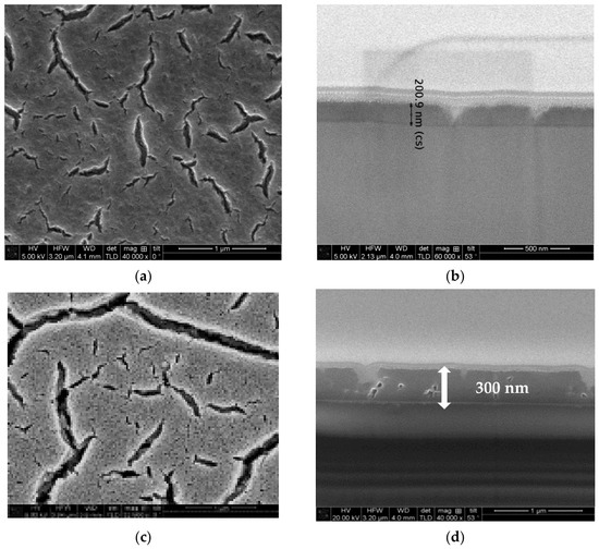
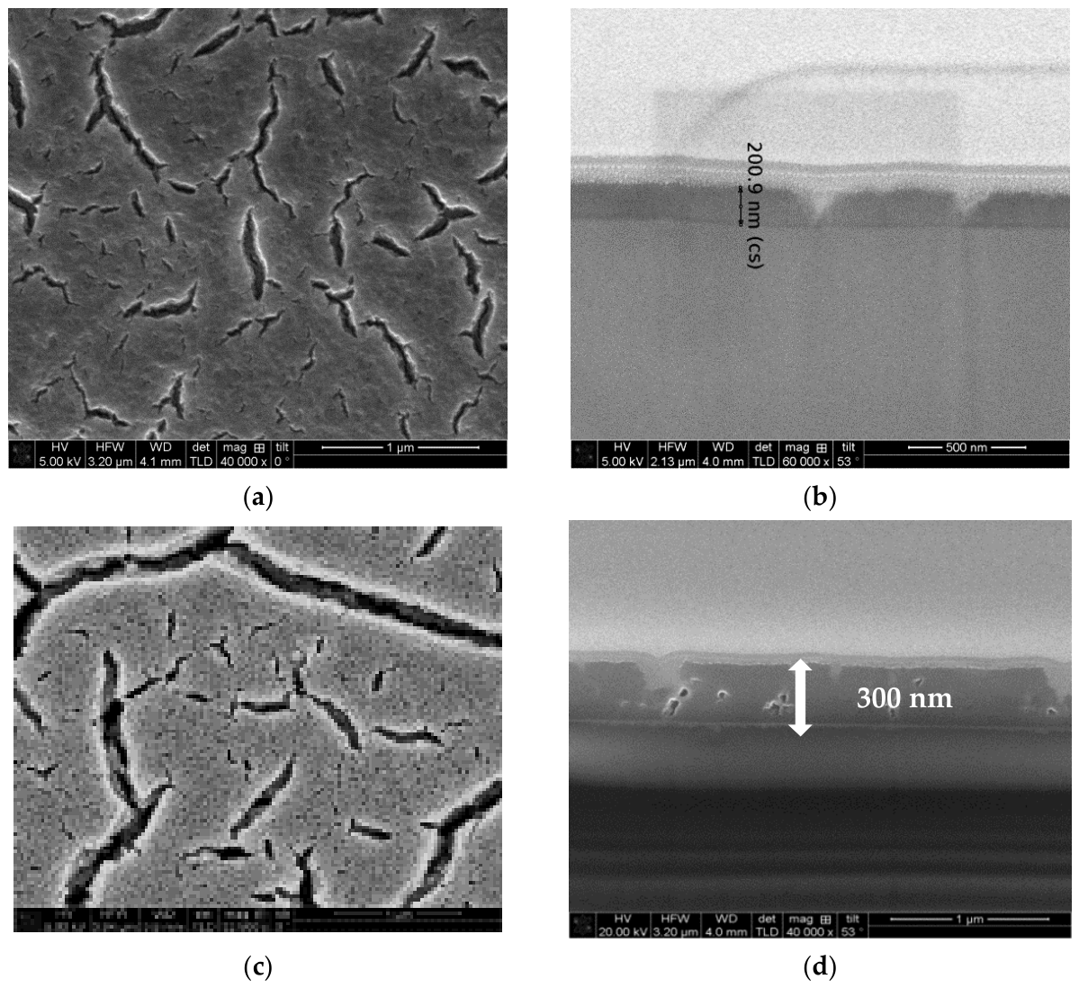
The morphological properties of the multilayered TiO2 sol–gel films were analyzed by the FESEM method in order to reveal the impact of substrate type—glass or ITO. The XRD study showed that substrate type influences film crystallinity and crystallite sizes. The FESEM images of the TiO2 films obtained on the glass substrate are shown in Figure 5. The films presented in Figure 5a,b are the two-layered coating annealed at 300 °C/60 min in air, and the micrographs exhibit the film surface morphology (Figure 5a) and a cross-sectional view (Figure 5b). The FESEM images reveal many cracks on the film surface. The film thickness is around 200 nm. The cracking could have been due to a thermal expansion mismatch [30,31].
Figure 5.
FESEM images of sol–gel TiO2 films deposited on glass substrates: (a) surface topography and (b) cross-sectional view of the two-layered film annealed at 300 °C/60 min; (c) surface topography and (d) cross-sectional view of the three-layered film annealed at 500 °C/60 min.
Increasing the number of layers (three layers) and the annealing temperature (500 °C) (see Figure 5c,d) resulted in the evolution of film cracking and higher thermal stress, inducing an increase in the width and in the shape of the cracks. The film thickness is 300 nm, derived from Figure 5d.
FESEM observation indicates that the prepared sol solution and the chosen technological parameters (spin rate and thermal treatments) for depositing TiO2 films on glass substrates lead to film cracking.
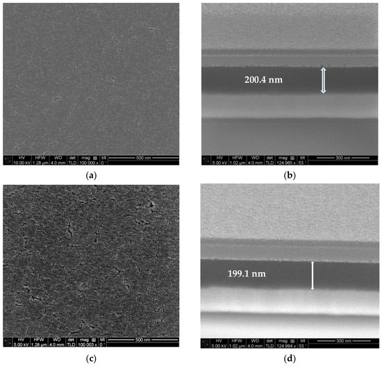
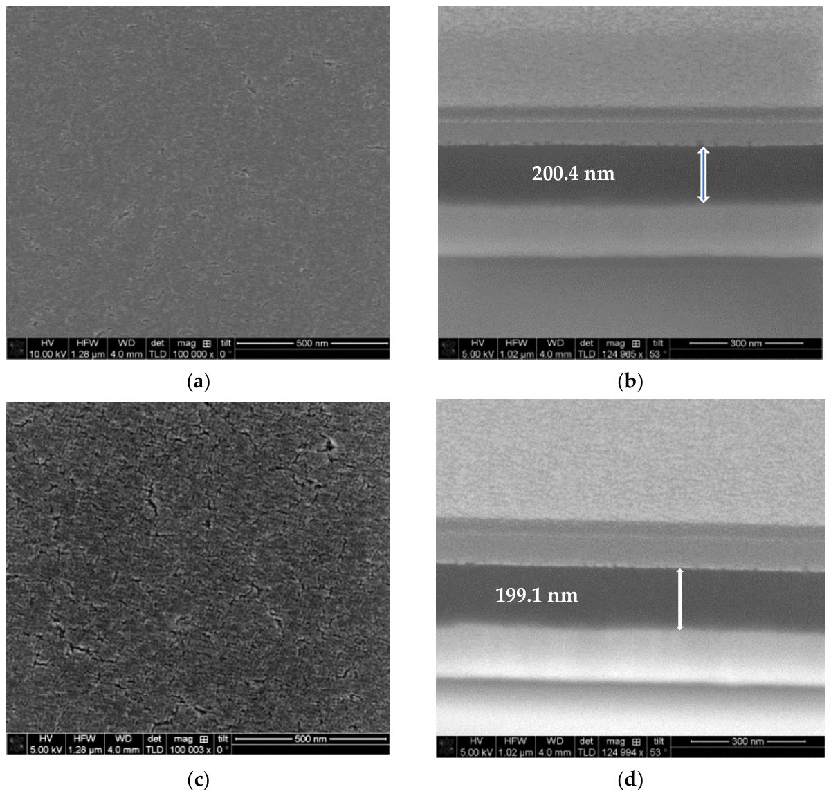
A FESEM study was performed for the TiO2 films obtained on ITO substrates, and the micrographs are shown in Figure 6, Figure 7 and Figure 8. The films were deposited under the same technological conditions as the TiO2 films fabricated on glass substrates. The thermal treatments were performed by keeping the same heating time (60 min) and temperatures as well as a heating and cooling rate of 10 °C/min.
Figure 6.
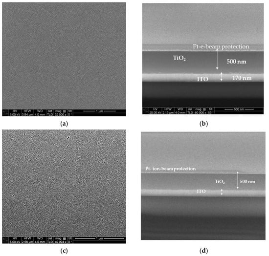
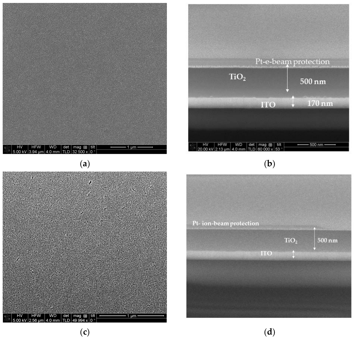
FESEM images of sol–gel two-layered TiO2 films deposited on ITO substrates: (a) surface topography and (b) cross-sectional view of the 300 °C annealed sample; (c) surface topography and (d) cross-sectional view of the 400 °C annealed sample.
Figure 7.
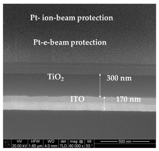
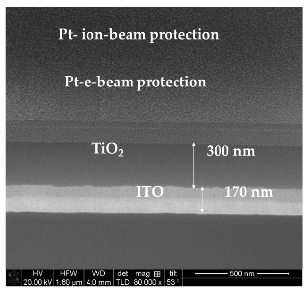
FESEM cross-section image of the sol–gel three-layered TiO2 films deposited on ITO substrates and annealed at 300 °C.
Figure 8.
FESEM images of the sol–gel five-layered TiO2 films deposited on ITO substrates: (a) surface topography and (b) cross-sectional view of the 400 °C annealed sample; (c) surface topography and (d) cross-sectional view of the 500 °C annealed sample.
Figure 6 reveals the morphology of the two-layered TiO2 films deposited on ITO substrates after annealing at 300 and 400 °C. The FESEM examination exposed quite different surface characteristics compared to the films obtained on glass substrates. The topography images (Figure 6a,c) reveal a very smooth, uniform and homogenous film morphology with small-grained structures. No surface cracks are observed. Raising the annealing temperature up to 400 °C induces the grains to grow larger and to pack closer together, improving film uniformity and smoothness. The two samples possess similar film thicknesses, around 200 nm, as can be deduced from the cross-section views (Figure 6b,d). There is no change in film thickness with an increase in annealing temperature.
Figure 7 presents a FESEM cross-section micrograph of the three-layered titanium dioxide films treated at 300 °C. The film thickness is determined to be 300 nm. No cracking and defects are detected.
The FESEM micrographs of the five-layered TiO2 films treated at 400 and 500 °C (see Figure 8) display very smooth and uniform surfaces. The sol–gel TiO2 films on the ITO substrate remain crack-free. The film thickness is 500 nm, independent of annealing temperatures. In contrast to the TiO2 films spin coated on glass substrates, cracking of the films deposited on the ITO glass was prevented.
FESEM investigation revealed two important conclusions. The sol–gel TiO2 films deposited on ITO substrates have homogeneous nucleation and smooth surface coverage with tiny grains. In comparison, the films on glass have a rougher surface with crack formation. The second conclusion is that one TiO2 layer of the sol–gel process results in a 100 nm-thick film, and film thickness grows linearly with the number of layers. This confirms our previous study [16]. The linear relationship between the number of layers and the final film thickness allows us to predict the film growth and to adjust it in accordance with the desired thickness. It has also been proven that film thickness is independent of substrate type and of high-temperature annealing.
3.4. Optical Properties
An optical characterization of the sol–gel TiO2 films was carried out, starting with spectrophotometric measurements of the coatings obtained on glass substrates. Figure 9 presents the transmittance and the reflectance spectra of the TiO2 films with one, three and five layers after annealing at 400 °C. The measured spectral range is 240–1800 nm. The transmittance spectra display strong absorption below 350 nm.
Figure 9.
Transmittance (solid lines) and reflectance (dot lines) spectra of TiO2 films on glass substrates with one, three and five layers and annealed at 400 °C.
The decrease in transmittance in the UV region can be attributed to the semiconducting nature of TiO2 films due to the existence of a band gap [13]. The absorption edges of the samples differ. It can be seen that film transmittance drops with an increase in the number of layers, and interference fringes appear in the spectra of the three- and five-layered films (Figure 9). Transparency worsens due to film thickness as the thickness changes from 100 nm up to 500 nm (five-layered coating). Film thickness was determined from the FESEM study. The other reasons for the lower transparency of the thicker films include the bigger crystallite sizes (XRD data), the films’ poor microstructure and the presence of cracks (FESEM images).
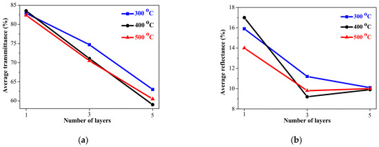
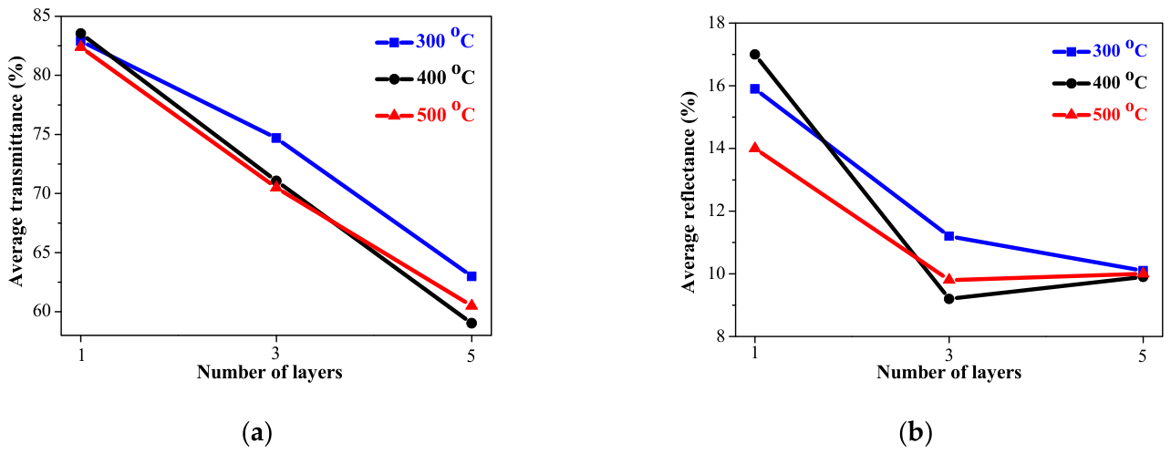
This conclusion is verified by the estimated average values of transmittance and reflectance in the visible spectral range of 450–700 nm. The data are given in Figure 10. It is observed that film transparency is strongly related to film thickness and to thermal treatments. Reflectance shows a similar tendency to decrease with an increasing film thickness. This indicates that thicker TiO2 films have increased light absorption and scattering.
Figure 10.
Estimated average values of (a) transmittance and (b) reflectance (for the visible spectral range of 450–700 nm) of TiO2 films on glass substrates annealed at 300, 400 and 500 °C independent of the number of layers. The bare glass possesses an average transmittance value of 91.2%, and the average reflectance is 7.4%.
The refractive index, n, is an important parameter for the optical characterization of thin films. The refractive index has been calculated from the measured reflectance spectra of TiO2 films (450–700 nm) deposited on glass substrates by using the following relation [32]:
where k is the extinction coefficient, and R is the reflectance. If k << n, then
Figure 11a displays the obtained average values (in the visible spectral range of 450–700 nm) of the refractive index of the TiO2 films deposited on glass substrates and annealed at 300–500 °C as a function of the number of layers. The refractive index values vary in the range of 1.87 up to 2.41, being strongly dependent on the number of layers and annealing procedures.
Figure 11.
The variation in (a) the average refractive index (for the visible spectral range of 450–700 nm) and (b) the optical band gap values, depending on the number of layers and annealing temperatures (300–500 °C). TiO2 films were deposited on glass substrates.
The optical band gap was estimated from the first derivative of transmittance versus energy [18,33]. The obtained optical band gap data as a function of the number of layers for TiO2 film/glass are presented in Figure 11b. The optical band gap values decrease from 3.75–3.78 eV (one-layered films) to 3.51–3.54 eV (five-layered films). Band-gap narrowing is observed with an increase in the thickness of the sol–gel TiO2 films. This effect can be due to either film thickness [34] or/and to the crystalline nature of the studied films [34]. As the number of layers and the film thickness increase, the light absorption and surface roughness also increase, as can be seen from the transmittance spectra. Similar findings have been obtained by others [35]. An increase in film thickness can generate donor levels near the conduction band. This leads to narrowing of the optical band gap [36]. Another possible contribution can be the presence of Ti3+ states, as it has been reported that this oxidation state, together with oxygen vacancies, can provoke band-gap narrowing [27]. The obtained values are in agreement with the literature data for TiO2 materials [21,37,38].
The widening of the optical band gap of the thin sol–gel TiO2 films compared to the bulk anatase titania of 3.2 eV can be explained by two factors: (i) the disordered and defected film structure and the presence of an amorphous phase [38]: XRD analysis reveals that the three-layered TiO2 films obtained on glass substrates possess an amorphous structure, and the five-layered sample has some crystallization with amorphous fraction after annealing at 300 °C. Annealing at 500 °C indicates a polycrystalline structure with broad XRD lines at (004), (200), (105), (211) and (204), a sign of very tiny crystallites and (ii) the Quantum Confinement Effect: small crystallite sizes can shift the absorption edge [39].
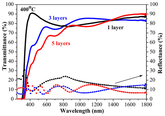
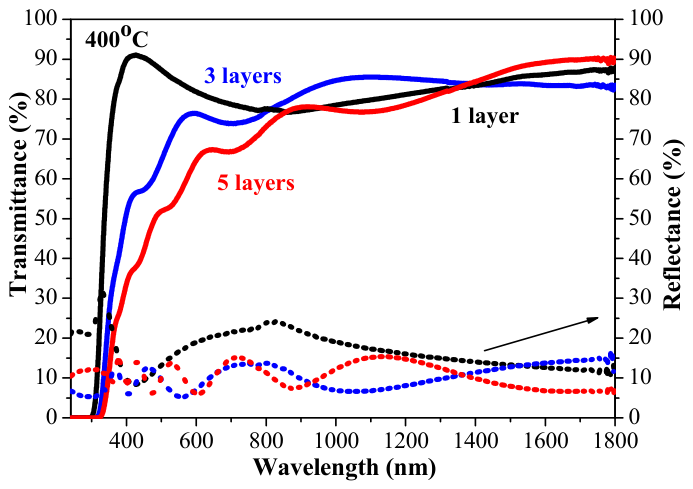
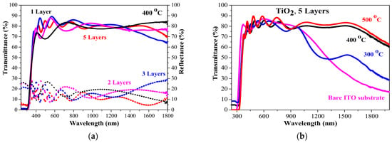
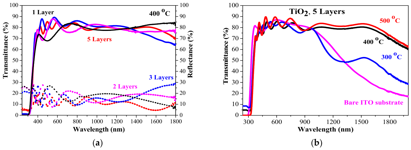
The optical properties of the thin sol–gel TiO2 films on ITO substrates display different behaviors. The titanium dioxide films show very high transmittance in the visible spectral range. This excellent transparency is maintained, regardless of the number of layers (with a corresponding film thickness of 100 to 500 nm) (see Figure 12a) and of an increase in annealing temperature (from 300 to 500 °C; see Figure 12b). Compared with the optical spectra of the TiO2 films deposited on the glass substrate, the transparency of these samples is higher, although an ITO substrate has lower optical transmittance than bare glass. The substrate effect is proven in the film structure and in the film morphology, as XRD and FESEM analyses revealed. The film morphology of the TiO2 films on ITO substrates is smooth, uniform and homogenous, which leads to better optical performance.
Figure 12.
Transmittance (solid lines) and reflectance (dot lines) spectra of (a) TiO2 films with one, two, three and five layers and annealed at 400 °C, and (b) five-layered films annealed at 300, 400 and 500 °C. The used substrate is ITO-covered glass.
As can be calculated from the transmittance spectra in Figure 12a, the average transmittance values are 74.1%, 82.3%, 83.4 5 and 81.8% for the one-, two-, three- and five-layered coatings annealed at 400 °C. The corresponding average reflectance values are 18.9%, 13.9%, 16.0% and 12.9% for the one-, two-, three- and five-layered TiO2 films, respectively. It must be noted that a bare ITO substrate has an average transmittance value of 85.7%, and the average reflectance value is 13.07% in the spectral range of 450–700 nm. The finding that the sol–gel TiO2 films achieved comparable transmittance of bare ITO substrates indicates that these films are suitable for integration in transparent solar cells and transparent electronics without causing significant optical loss [40,41].
Annealing at different temperatures also has a negligible influence on optical transmittance. Figure 12b exhibits the transmittance spectra of the thickest TiO2 films obtained on the ITO substrate and annealed at 300, 400 and 500 °C. The average transmittance values of the five-layered TiO2 films are in the range of 81.8–84.0% after thermal treatments at 300, 400 and 500 °C. The films possess a nanocrystalline structure in the anatase phase with nanosized crystallites (see Table 1). The FESEM images also confirm this conclusion and prove the very smooth and uniform surfaces (see Figure 6, Figure 7 and Figure 8).
The high transparency of the sol–gel TiO2 films deposited on ITO substrates indicates low surface roughness, smoothness and good homogeneity. It can be concluded that sol–gel multilayered TiO2 films deposited on ITO substrates possess excellent optical quality. They can be considered as appropriate candidates for applications in transparent solar cells.
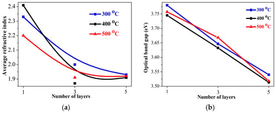
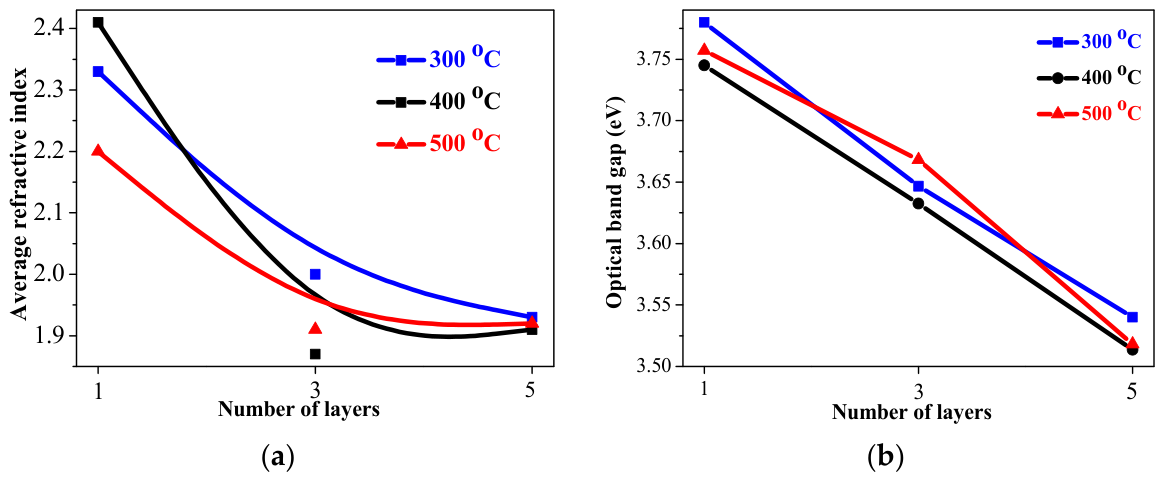
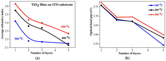
The refractive index of the sol–gel TiO2 films on ITO substrates was determined using Equation (4). The results are presented in Figure 13a. High values above 2.1 are reported for the TiO2 films on ITO-coated substrates [42]. It is quite clear that the refractive index values increase with an increase in annealing temperature from 300 to 500 °C. Similar observations have been made by others [37,43]. The obtained refractive indices are within the reported values [5,44,45]. Higher refractive index values indicate that the films have lower porosity [46].
Figure 13.
The dependence of (a) the average refractive index (for the spectral range of 450–700 nm) and (b) optical band gap values on the number of layers of TiO2 films deposited on ITO substrates. The films were annealed at 300–500 °C.
Figure 13b presents the estimated optical band gap values of the TiO2 films on ITO substrates, depending on the number of layers (film thickness) and on the annealing temperatures. The optical band gap (Eg) of TiO2 films is affected by the crystal structure (amorphous, anatase, or rutile), crystallite sizes, defects, deposition methods, oxygen vacancy concentration, etc. [46]. Narrowing of the optical band gap with an increase in film thickness has previously been reported [18,47]. The film thickness dependence of the optical band gap for the sol–gel TiO2/ITO samples can also be attributed to the existence of surface oxygen vacancy [34].
A comparison of the obtained data for the refractive index and the optical band gap of the TiO2 films deposited on the two types of substrates reveals interesting features. The tendency of the values of the two optical parameters to decrease with an increase in film thickness is observed for the films deposited on both substrates. However, the variation in refractive index and optical band gap with an increase in annealing temperature is distinctly different.
The refractive index and the optical band gap values of the TiO2 films obtained on glass substrates become smaller with annealing. By contrast, the optical characteristics (n, Eg) of the sol–gel films on ITO substrates increase with raising the annealing temperature. The increase in Eg with annealing can be assigned to a reduction in the oxygen vacancies and the quantum-size effect, as it is known that the smaller the particle size, the higher the band gap energy [48,49]. This effect can be due to the substrate type and, correspondingly, to the crystalline structure of the films (see XRD results). These two factors have a considerable effect on the refractive index. The refractive index values of the TiO2 films on the glass substrates are smaller than the corresponding values of the films obtained on ITO.
The optical study suggests that the TiO2 films obtained on glass are porous with the presence of structural defects. This is confirmed by the FESEM observations. The higher refractive index of the TiO2 films/ITO is attributed to the increased film density [15]. The improved film structure of the spin-coated TiO2 films on the ITO substrate is proved by the FESEM analysis, where a dense small-grained structure can be observed (see Figure 8).
3.5. Electrical Properties of Sol–Gel TiO2 Films
Sheet resistance was measured by a four-point probe of the sol–gel films deposited on glass substrates. The sheet resistance of TiO2 films is an important parameter for understanding their electrical properties and for their different applications. The values of TiO2 films have been reported in a wide range, depending on the layer thickness, deposition method, thermal treatments and doping [50]. TiO2 can exhibit dielectric and conductive properties, depending on the crystal structure and doping. In its undoped form, TiO2 possesses a high dielectric constant and can be used as a dielectric. In a thin-film form, structural defects can be created in the TiO2 structure, including titanium suboxides and oxygen vacancies. These defects lead to a rise in conductivity.
The studied sol–gel TiO2 films obtained on glass substrates show a sheet resistance of 340 to 690 Ω/sq with an increasing number of layers after annealing at 300 °C. After 400 and 500 °C, the values are almost the same, within the range of 640–690 Ω/sq.
The work function of thin metal oxide films has been found to be important for device properties and performance, as it affects the band alignments of interfaces in TiO2/metal contacts forming Schottky barriers, TiO2/p-type semiconductor interfaces forming p-n heterojunctions, and TiO2/liquid junctions related to redox potentials [37]. Its knowledge is vital for high-efficient solar cells; oxide electronics; electrocatalysts; and applications utilizing thermionic electron or field emission physics, such as Schottky junctions, thermionic energy converters, and vacuum cathodes for high power microwave sources [51]. Reported WF values of TiO2 films are varied, being in the range of 4.5–5.2 eV [51,52]. The work function depends on surface defects, oxygen vacancies, deposition methods, annealing and the presence of certain surface states [53,54].
The measured WF values of the sol–gel TiO2 films obtained on Si and ITO substrates are shown in Table 2 and Table 3. The Kelvin probe measurements were done in an ambient atmosphere and at room temperature.
Table 2.
Work function values of TiO2 films deposited on silicon wafers. The work function of the used Si substrate is 4.35 eV.
Table 3.
Work function values of TiO2 films deposited on ITO substrates. The measured WF of the bare substrate is 5.20 eV.
The studied sol–gel films possess higher work function values than that of bulk TiO2 (typically 4.2 eV). This can be due to the quantum confinement effect, where the nanometric sizes of the particles limit the mobility of electrons and raises the energy levels. Therefore, more energy is required to release an electron, which leads to a higher work function in nanocrystalline films compared to bulk TiO2 [55,56]. It has also been reported that the WF values vary with thickness; this was found for sputtered ITO films [57]. It has been reported [56,58] that TiO2 nanoparticles on Si substrates show WF values ranging from 4.49 to 4.57 eV, strongly influenced by particle-size variation (from 3 nm to 85 nm). Other researchers found lower WF values (4.22 eV) for 22 nm-thick ALD TiO2 films on FTO substrates [58]. It is worth mentioning that the work function of anatase TiO2 single crystal is reported to be 4.40–4.46 eV, and for polycrystalline anatase films, the values are 4.59 eV and 4.30 eV [59].
4. Conclusions
This research proves the successful sol–gel spin-coating deposition of TiO2 films on different types of substrates: Si, glass and ITO. The deposition of two layers on glass and ITO substrates results in 200 nm. It was found from FESEM cross-section images that film thickness depends linearly on the number of layers. This linear thickness growth is independent of annealing temperature and of substrate type. It was found that substrate type strongly reflects film crystallization. The sol-gel TiO2 films obtained on glass substrates crystallized in the anatase phase only after the highest annealing at 500 °C. In contrast, the sol–gel TiO2 films deposited on ITO substrates reveal a polycrystalline structure at the lower annealing temperature of 300 °C. FESEM images demonstrate that glass is not a suitable substrate for sol–gel spin-coated TiO2 films as film cracking and a rough surface morphology are detected. Meanwhile, the titanium dioxide films obtained on ITO substrates display a uniform, tiny-grained and homogenous surface morphology. These films are found to be highly transparent in the visible spectral range (up to 85%), and their transmittance is almost not affected by thermal treatments and film thickness. The transparency of the TiO2 films on the glass substrate is reduced with an increase in the number of layers and the annealing temperatures. The determined refractive index and optical band gap are discussed. The work function (WF) of TiO2 films depends on the number of layers, annealing temperature and type of substrate. The WF values are in range of 4.31–4.80 eV for TiO2/Si and 4.51–5.16 for the TiO2 films on the ITO substrate. The obtained results of the structural, morphological, optical and electrical studies are encouraging. This research proposes that sol–gel TiO2 films deposited on ITO substrates can be applied in transparent photovoltaic and optoelectronic devices.
Author Contributions
Conceptualization, T.I. and A.H.; methodology, T.I.; validation, T.I., A.H. and N.P.; formal analysis, T.I.; investigation, T.I., A.H. and N.P.; resources, A.H.; data curation, T.I., A.H. and N.P.; writing—original draft preparation, T.I.; writing—review and editing, T.I., A.H. and N.P.; visualization, A.H.; supervision, T.I. All authors have read and agreed to the published version of the manuscript.
Funding
This research was funded by the Bulgarian National Science Fund (BNSF), grant number KP-06-N78/7, under the project Development and Investigation of Metal Oxide Heterostructures for Transparent Solar Cells.
Data Availability Statement
The original contributions presented in this study are included in the article. Further inquiries can be directed to the corresponding author.
Conflicts of Interest
The authors declare no conflicts of interest.
References
- Kumi-Barimah, E.; Penhale-Jones, R.; Salimian, A. Phase evolution, morphological, optical and electrical properties of femtosecond pulsed laser deposited TiO2 thin films. Sci. Rep. 2020, 10, 10144. [Google Scholar] [CrossRef] [Scilit] [PubMed]
- Soussi, A.; Hssi, A.A.; Boujnah, M.; Boulkadat, L.; Abouabassi, K.; Asbayou, A.; Elfanaoui, A.; Markazi, R.; Ihlal, A.; Bouabid, K. Electronic and Optical Properties of TiO2 Thin Films: Combined Experimental and Theoretical Study. J. Electon. Mater. 2021, 50, 4497–4510. [Google Scholar] [CrossRef] [Scilit]
- Dayan, A.; Fleminger, G. Titanium Dioxide in Biomedical and Environmental Nanotechnology: From Photocatalytic Detoxification to Targeted Therapeutics. Molecules 2026, 31, 1197. [Google Scholar] [CrossRef] [Scilit] [PubMed]
- Liu, X.; Fu, J. Electronic and elastic properties of the tetragonal anatase TiO2 structure from first principle calculation. Optik 2020, 206, 164342. [Google Scholar] [CrossRef] [Scilit]
- Hassanien, A.S.; Akl, A.A. Optical characterizations and refractive index dispersion parameters of annealed TiO2 thin films synthesized by RF-sputtering technique at different flow rates of the reactive oxygen gas. Phys. B Condens. Matter. 2020, 576, 411718. [Google Scholar] [CrossRef] [Scilit]
- Wach, A.; Zou, X.; Wojtaszek, K.; Kayser, Y.; Garlisi, C.; Palmisano, G.; Sá, J.; Szlachetko, J. Towards understanding the TiO2 doping at the surface and bulk. X-Ray Spectrom. 2023, 52, 261–268. [Google Scholar] [CrossRef] [Scilit]
- Ghamsari, M.S.; Bahramian, A.R. High transparent sol-gel derived nanostructured TiO2 thin film. Mater. Lett. 2008, 62, 361–364. [Google Scholar] [CrossRef] [Scilit]
- Padmanabhan, N.T.; Thomas, N.; Louis, J.; Mathew, D.T.; Ganguly, P.; John, H.; Pillai, S.C. Graphene coupled TiO2 photocatalysts for environmental applications: A review. Chemosphere 2021, 271, 129506. [Google Scholar] [CrossRef] [Scilit] [PubMed]
- Goutham, C.; Ashok Kumar, K.V.; Kumar Raavi, S.S.; Subrahmanyam, C.; Asthana, S. Enhanced electrical and photocatalytic activities in Na0.5Bi0.5TiO3 through structural modulation by using anatase and rutile phases of TiO2. J. Mater. 2022, 8, 18–29. [Google Scholar] [CrossRef] [Scilit]
- Conti, P.P.; Andre, R.S.; Mercante, L.A.; Fugikawa-Santos, L.; Correa, D.S. Discriminative detection of volatile organic compounds using an electronic nose based on TiO2 hybrid nanostructures. Sens. Actuators B Chem. 2021, 344, 130124. [Google Scholar] [CrossRef] [Scilit]
- Kumar, N.; Nguyen, T.T.; Park, H.H.; Lee, K.; Kim, S.M.; Kim, J. Role of substrate architecture and modelling on photocurrent and photovoltage in TiO2/NiO transparent photovoltaic. Mater. Res. Bull. 2021, 142, 111421. [Google Scholar] [CrossRef] [Scilit]
- Nguyen, T.T.; Patel, M.; Kim, J.W.; Lee, W.; Kim, J. Functional TiO2 interlayer for all-transparent metal-oxide photovoltaics. J. Alloys Compd. 2020, 816, 152602. [Google Scholar] [CrossRef] [Scilit]
- Khan, M.I.; Bhatti, K.A.; Qindeel, R.; Althobaiti, H.S.; Alonizan, N. Structural, electrical and optical properties of multilayer TiO2 thin films deposited by sol-gel spin coating. Results Phys. 2017, 7, 1437–1439. [Google Scholar] [CrossRef] [Scilit]
- Mulus, D.S.; Permana, M.D.; Deawati, Y.; Eddy, D.R. A current review of TiO2 thin films: Synthesis and modification effect to the mechanism and photocatalytic activity. Appl. Surf. Sci. Adv. 2025, 27, 100746. [Google Scholar] [CrossRef] [Scilit]
- Sta, I.; Jlassi, M.; Hajji, M.; Boujmil, M.F.; Jerbi, R.; Kandyla, M.; Kompitsas, M.; Ezzaouia, H. Structural and optical properties of TiO2 thin films prepared by spin coating. J. Sol-Gel Sci. Technol. 2014, 72, 421–427. [Google Scholar] [CrossRef] [Scilit]
- Ivanova, T.; Harizanova, A.; Petkov, N.; Dulev, V.; Benkovski, A.; Ganchev, M. Titanium dioxide thin films prepared on different substrates by sol–gel process: Optical and morphological Properties. J. Phys. Conf. Ser. 2025, 2952, 012002. [Google Scholar] [CrossRef] [Scilit]
- Harizanov, O.; Harizanova, A. Development and investigation of sol–gel solutions for the formation of TiO2 coatings. Sol. Energy Mater. Sol. Cells 2000, 63, 185–195. [Google Scholar] [CrossRef] [Scilit]
- Guillén, C. Band Gap Energy and Lattice Distortion in Anatase TiO2 Thin Films Prepared by Reactive Sputtering with Different Thicknesses. Materials 2025, 18, 2346. [Google Scholar] [CrossRef] [Scilit] [PubMed]
- Parveen, B.; Hassan, M.; Khalid, Z.; Riaz, S.; Naseem, S. Room-temperature ferromagnetism in Ni-doped TiO2 diluted magnetic semiconductor thin films. J. Appl. Res. Technol. 2017, 15, 132–139. [Google Scholar] [CrossRef] [Scilit]
- Umirzakov, B.E.; Isaxanov, Z.A.; Bekpulatov, I.R.; Kosimov, I.O.; Maxmudov, M.M.; Imanova, G. Study of the influence of temperature and gamma radiation on the crystal structure of a thin TiO2 coating obtained on A Si (111) surface. Phys. Lett. A 2026, 518, 131519. [Google Scholar] [CrossRef] [Scilit]
- Mathews, N.R.; Morales, E.R.; Cortes-Jacome, M.A.; Toledo Antonio, J.A. TiO2 thin films—Influence of annealing temperature on structural, optical and photocatalytic properties. Sol. Energy 2009, 83, 1499–1508. [Google Scholar] [CrossRef] [Scilit]
- Chi, M.; Sun, X.; Lozano-Blanco, G.; Tatarchuk, B.J. XPS and FTIR investigations of the transient photocatalytic decomposition of surface carbon contaminants from anatase TiO2 in UHV starved water/oxygen environments. Appl. Surf. Sci. 2021, 570, 151147. [Google Scholar] [CrossRef] [Scilit]
- Zou, J.; Gao, J.; Xie, F. An amorphous TiO2 sol sensitized with H2O2 with the enhancement of photocatalytic activity. J. Alloys Compd. 2010, 497, 420–427. [Google Scholar] [CrossRef] [Scilit]
- Nobre, F.X.; Pesso, W.A.; Ruiz, Y.; Bentes, V.L.I.; Silva-Moraes, M.O.; Silva, T.M.C.; Rocco, M.L.M.; Larrude, D.R.G.; de Matos, J.M.E.; Couceiro, P.R.C.; et al. Facile synthesis of nTiO2 phase mixture: Characterization and catalytic performance. Mater. Res. Bull. 2019, 109, 60–71. [Google Scholar] [CrossRef] [Scilit]
- Qahtan, T.F.; Owolabi, T.O.; Saleh, T.A. X-ray photoelectron spectroscopy of surface-treated TiO2 mesoporous film by 500B eV argon ion beam. J. Mol. Liq. 2024, 393, 123556. [Google Scholar] [CrossRef] [Scilit]
- Idriss, H. On the wrong assignment of the XPS O1s signal at 531–532 eV attributed to oxygen vacancies in photo- and electro-catalysts for water splitting and other materials applications. Surf. Sci. 2021, 712, 121894. [Google Scholar] [CrossRef] [Scilit]
- Bharti, B.; Kumar, S.; Lee, H.N.; Kumar, R. Formation of oxygen vacancies and Ti3+ state in TiO2 thin film and enhanced optical properties by air plasma treatment. Sci. Rep. 2016, 6, 632355. [Google Scholar] [CrossRef] [Scilit] [PubMed]
- Korduban, O.M.; Kryshchuk, T.V.; Kandyba, V.O.; Trachevskii, V.V. XPS Studies of the surface of TiO2:Ag nanopowders. Chem. Phys. Technol. Surf. 2020, 11, 547–555. [Google Scholar] [CrossRef] [Scilit]
- Diebold, U.E.; Madey, T.E. TiO2 by XPS. Surf. Sci. Spectra 1996, 4, 227–231. [Google Scholar] [CrossRef] [Scilit]
- Zhou, F.; Liang, K.M.; Shao, H. Study on the Cracking of SiO2-TiO2 Films Prepared by Sol-Gel Method. Mater. Sci. Forum 2005, 475–479, 1227–1230. [Google Scholar]
- Lopez, L.; Daoud, W.A.; Dutta, D. Preparation of large scale photocatalytic TiO2 films by the sol–gel process. Surf. Sci. Technol. 2010, 205, 251–257. [Google Scholar] [CrossRef] [Scilit]
- El-Desoky, M.M.; Ali, M.A.; Afifi, G.; Imam, H. Annealing effects on the structural and optical properties of growth ZnO thin films fabricated by pulsed laser deposition (PLD). J. Mater. Sci. Mater. Electron. 2014, 25, 5071–5077. [Google Scholar] [CrossRef] [Scilit]
- Serrar, H.; Mecibah, F.Z.; Kribes, I.; Bouachiba, Y.; Mammeri, A.; Bouabellou, A.; Retima, M.; Boughelout, A.; Taabouche, A.; Aouati, R. Argon flow rate effects on the optical waveguide properties of DC sputtered TiO2 thin films. Opt. Mater. 2023, 135, 113259. [Google Scholar] [CrossRef] [Scilit]
- Ennaceri, H.; Boujnah, M.; Taleb, A.; Khaldoun, A.; Araoz, R.; Ennaoui, A.; El Kenz, A.; Benyoussef, A. Thickness effect on the optical properties of TiO2-anatase thin films prepared by ultrasonic spray pyrolysis: Experimental and ab initio study. Int. J. Hydrogen Energy 2017, 42, 19467–19480. [Google Scholar] [CrossRef] [Scilit]
- Gurakar, S.; Ot, H.; Horzum, S.; Serin, T. Variation of structural and optical properties of TiO2 films prepared by DC magnetron sputtering method with annealing temperature. Mater. Sci. Eng. B 2020, 262, 114782. [Google Scholar] [CrossRef] [Scilit]
- Ali, H.S.; Jasim, R.I.; Magid, H.C.; Hussein, S.A.; Chiad, S.S.; Habubi, N.F.; Kadhim, Y.H.; Jadan, M. Influence of thickness on the physical properties of nanostructured TiO2 thin films for nitrogen dioxide gas sensor. Dig. J. Nanomater. Biostruct. 2025, 20, 595–608. [Google Scholar] [CrossRef] [Scilit]
- Yang, C.; Fan, H.; Xi, Y.; Chen, J.; Li, Z. Effects of depositing temperatures on structure and optical properties of TiO2 film deposited by ion beam assisted electron beam evaporation. Appl. Surf. Sci. 2008, 254, 2685–2689. [Google Scholar] [CrossRef] [Scilit]
- Landmann, M.; Köhler, T.; Köppen, S.; Rauls, E.; Frauenheim, T.; Schmidt, W.G. Fingerprints of order and disorder in the electronic and optical properties of crystalline and amorphous TiO2. Phys. Rev. B 2012, 86, 064201. [Google Scholar] [CrossRef] [Scilit]
- Rincón-Barón, L.A.; Forero-Carvajal, M.P.; Ramírez-Alemán, L.G.; Mejía-Gómez, A.E.; Salcedo-Reyes, J.C.; Carrascal-Camacho, A.K.; Velez, C.; Pedroza-Rodríguez, A.M. Development of TiO2 Films by Sol–Gel/Sedimentation for the Inactivation of Multidrug-Resistant Escherichia coli and Salmonella Typhimurium in Greywater. Catalysts 2025, 15, 1115. [Google Scholar] [CrossRef] [Scilit]
- Wang, X.; Wu, G.; Zhou, B.; Shen, J. Optical Constants of Crystallized TiO2 Coatings Prepared by Sol-Gel Process. Materials 2013, 6, 2819–2830. [Google Scholar] [CrossRef] [Scilit] [PubMed]
- Arifin, N.M.; Mhd Noor, E.E.; Mohamad, F.; Mohamad, N.; Mohamed Muzni, N.H. Enhancing the Properties of Nanostructure TiO2 Thin Film via Calcination Temperature for Solar Cell Application. Energies 2024, 17, 3415. [Google Scholar] [CrossRef] [Scilit]
- Djehiche, N.E.; Saidi, H.; Derbali, A.; Ataf, A.; Khetta, O.B.; Aida, M.S.; Bourhefir, R.; Toumi, R.; Youcef, R.; Bouhdjer, A. Sol–gel synthesis and spin-coating Nb-doped TiO2 anatase thin films. J. Sol.-Gel Sci. Technol. 2026, 117, 79. [Google Scholar] [CrossRef] [Scilit]
- Baqandwan, H.; Samsuri, S.A.M.; Halim, M.M.; Pakhuruddin, M.Z. Nanostructured TiO2 thin films sputtered at room temperature as electron transport layer for flexible perovskite solar cell applications: Impact of varying RF power. Phys. B Condens. Matter 2024, 679, 415788. [Google Scholar] [CrossRef] [Scilit]
- Zhou, L.; Zhang, X.; Wang, Z.; Fu, J.; Wu, S.; Hou, P.; Lu, J.; Xie, Y.; Liu, C.; Zhao, X.; et al. Aqueous-Processed TiO2-SiO2 Composite Antireflective Coating for Durable and Sustainable Photovoltaics. Colloids Surf. A Physicochem. Eng. Asp. 2026, 749, 141272. [Google Scholar] [CrossRef] [Scilit]
- Saha, D.; Ajimsha, R.S.; Rajiv, K.; Mukherjee, C.; Gupta, M.; Misra, P.; Kukreja, L.M. Spectroscopic ellipsometry characterization of amorphous and crystalline TiO2 thin films grown by atomic layer deposition at different temperatures. Appl. Surf. Sci. 2014, 315, 116–123. [Google Scholar] [CrossRef] [Scilit]
- Abdellatif, S.; Sharifi, P.; Kirah, K.; Ghannam, R.; Khalil, A.S.G.; Erni, D.; Marlow, F. Refractive index and scattering of porous TiO2 films. Microporous Mesoporous Mater. 2018, 264, 84–91. [Google Scholar] [CrossRef] [Scilit]
- Manna, D.; Mondal, K.; Karmakar, P.; Chakraborty, S. Deposition pressure assisted vacancy engineering of rf sputtered TiO2−x thin-films in argon plasma leading to smaller optical band gap and room temperature resistive switching properties. Appl. Surf. Sci. 2025, 703, 163343. [Google Scholar] [CrossRef] [Scilit]
- Bouachiba, Y.; Bouabellou, A.; Hanini, F.; Kermiche, F.; Taabouche, A.; Boukheddaden, K. Structural and optical properties of TiO2 thin films grown by sol-gel dip coating process. Mater. Sci.-Pol. 2014, 32, 1–6. [Google Scholar] [CrossRef] [Scilit]
- Fotsa-Ngaffo, F.; Caricato, A.P.; Romano, F. Optical properties of ITO/TiO2 single and double layer thin films deposited by RPLAD. Appl. Surf. Sci. 2009, 255, 9684–9687. [Google Scholar] [CrossRef] [Scilit]
- Alamgir; Khan, W.; Ahmad, S.; Hassan, M.; Naqvi, A.H. Structural phase analysis, band gap tuning and fluorescence properties of Co doped TiO2 nanoparticles. Opt. Mater. 2014, 38, 278–285. [Google Scholar] [CrossRef] [Scilit]
- Singh, S.; Sharma, V.; Sachdev, K. Investigation of effect of doping concentration in Nb-doped TiO2 thin films for TCO applications. J. Mater. Sci. 2017, 52, 11580–11591. [Google Scholar] [CrossRef] [Scilit]
- Kashiwaya, S.; Morasch, J.; Streibel, V.; Toupance, T.; Jaegermann, W.; Klein, A. The Work Function of TiO2. Surfaces 2018, 1, 73–89. [Google Scholar] [CrossRef] [Scilit]
- Pandey, A.; Singh, F.; Garg, A.; Kanjilal, D.; Kumar, L. Work function modulation and charge transport studies of 100 MeV Au7+ ions irradiated TiO2 films for optoelectronic devices. Opt. Mater. 2023, 143, 114180. [Google Scholar] [CrossRef] [Scilit]
- Yao, Q.; Li, S.; Dong, L.; Gu, P.; Liu, X.; Wang, F.; Yuan, G.; Yu, Z. Achieving tunable work function in MoOx thin films: A key to low-cost, high-performance organic electronics. Thin Solid Films 2025, 817, 140659. [Google Scholar] [CrossRef] [Scilit]
- Borodin, A.; Reichling, M. Characterizing TiO2 (110) surface states by their work function. Phys. Chem. Chem. Phys. 2011, 13, 15442–15447. [Google Scholar] [CrossRef] [Scilit] [PubMed]
- Musa, I.; Qamhieh, N.; Ghabboun, J.; Mahmoud, S.T. Investigation of tunable work function, electrostatic force microscopy and band structure of TiO2 nanoparticles using Kelvin probe force microscopy. Next Mater. 2025, 9, 101088. [Google Scholar] [CrossRef] [Scilit]
- Kumar, K.J.; Raju, N.R.C.; Subrahmanyam, A. Thickness dependent physical and photocatalytic properties of ITO thin films prepared by reactive DC magnetron sputtering. Appl. Surf. Sci. 2011, 257, 3075–3080. [Google Scholar] [CrossRef] [Scilit]
- Zlamalova, M.; Mansfeldova, V.; Tarabkova, H.; Krysova, H.; Kavan, L. Variable work function of semiconducting thin-film oxide electrodes: A case study of SnO2 and TiO2. J. Solid State Electrochem. 2023, 27, 1935–1943. [Google Scholar] [CrossRef] [Scilit]
- Mansfeldova, V.; Zlamalova, M.; Tarabkova, H.; Janda, P.; Vorokhta, M.; Piliai, L.; Kavan, L. Work Function of TiO2 (Anatase, Rutile, and Brookite) Single Crystals: Effects of the Environment. J. Phys. Chem. C 2021, 125, 1902–1912. [Google Scholar] [CrossRef] [Scilit]

Disclaimer/Publisher’s Note: The statements, opinions and data contained in all publications are solely those of the individual author(s) and contributor(s) and not of MDPI and/or the editor(s). MDPI and/or the editor(s) disclaim responsibility for any injury to people or property resulting from any ideas, methods, instructions or products referred to in the content. |
© 2026 by the authors. Licensee MDPI, Basel, Switzerland. This article is an open access article distributed under the terms and conditions of the Creative Commons Attribution (CC BY) license.