Abstract
ScAlMgO4 (SAM) is a promising substrate material for group III-nitride semiconductors. SAM has a lower lattice mismatch with III-nitride materials compared to conventionally used sapphire (Al2O3) and silicon substrates. Bulk SAM substrate has the issues of high cost and lack of large area substrates. Utilizing solid-phase epitaxy to transform an amorphous SAM on a sapphire substrate into a crystalline form is a cost-efficient and scalable approach. Amorphous SAM layers were deposited on 0001-oriented Al2O3 by sputtering and crystallized by annealing at a temperature greater than 850 °C. Annealing under suboptimal annealing conditions results in a larger volume fraction of a competing spinel phase (MgAl2O4) exhibiting themselves as crystal facets on the subsequently grown InGaN layers during MOCVD growth. InGaN on SAM layers demonstrated both a higher intensity and emission redshift compared to the co-loaded InGaN on GaN on sapphire samples, providing a promising prospect for achieving efficient longer-wavelength emitters.
1. Introduction
The group III-nitride material system has enabled numerous technologies including electronic and optoelectronic devices. InGaN-based LEDs can be used for emitters of different wavelengths by varying the indium content in the film. A higher indium concentration in the quantum well is required for longer emission wavelengths. An increasing indium content changes their bandgap from 0.7 eV to 3.4 eV, spanning the near IR to near UV range, respectively [1]. One of the most difficult aspects of the InGaN-based material synthesis is its lattice mismatch with the conventionally used GaN buffer layer, which is approximately 11% between GaN and InN [2,3,4,5]. Such a high lattice mismatch results in a high strain, causing dislocations in the crystalline structure and defect generation [1,2]. The use of a relaxed InGaN buffer layer reduces the lattice mismatch between the buffer layers and the active region of the emitters, enhancing the efficiency of the devices [6]. AlInGaP-based red emitters are conventionally used; however, size reduction results in a severe efficiency reduction [7,8,9], which is not a critical concern for nitride-based emitters [10,11,12]. Therefore, there is a critical need for a relaxed InGaN substrate technology. One of the methods to achieve relaxed InGaN is to grow an InGaN buffer layer on a suitable lattice-matched substrate such as ZnO (lattice-matched to In0.22Ga0.78N) [13,14,15,16,17] or ScAlMgO4 (SAM) (lattice-matched to In0.17Ga0.83N) [18,19,20]. Using a modified flexible underlayer to achieve relaxed InGaN has been studied, such as the porosification of Si-doped GaN [21,22,23,24] and thermal decomposition of underlying high-composition InGaN [25,26]. These methods have successfully demonstrated relaxed InGaN buffer layers and achieved different extents of emission redshifts, however, they also had different constraints. Deposition on ZnO requires a very low deposition temperature (<600 °C), porous GaN based substrates require additional fabrication steps, and thermal decomposition of high composition InGaN layer results in an increased dislocation density [14,18,26]. These constraints motivated us to pursue the study of accessible SAM substrates for high-composition InGaN synthesis. SAM has a lattice mismatch of 0% with In0.17Ga0.83N and ~2% with GaN, making it a suitable candidate for hetero-epitaxial growth of III-nitride materials [18,19,20]. The high substrate cost of bulk SAM substrates—USD8900 for 2 in diameter substrates—is quite limiting for academic research [27]. The solid-phase epitaxy (SPE) of amorphous SAM on sapphire followed by crystallization is a cost-efficient way to solve this issue. A problem associated with the creation of thin layers of SAM is that the crystallization of the SAM layer with unoptimized annealing conditions leads to the appearance of scandium-deficient regions on the surface, which lead to the formation of undesirable spinel-phase MgAl2O4 material [28]. The surface roughness of SPE-grown SAM is considerably higher than the other substrate technologies cited before due to its multi-crystallinity. In a previous study, Chen et al. demonstrated the synthesis of epitaxial SAM on a sapphire substrate with a preferred lower temperature of crystallization to constrain the formation of spinel-phase MgAl2O4 [28].
In this work, we present an improved crystallization method for SAM layers grown on a sapphire substrate and present Metal-Organic Chemical Vapor Deposition (MOCVD) growth of InGaN layers on crystalline SAM. The surface roughness and crystallinity were optimized by annealing SAM at different temperatures for various durations. The InGaN layers grown on SAM on sapphire demonstrated a higher photoluminescence (PL) intensity and a longer peak wavelength of emission compared to the same layers grown on a co-loaded reference GaN on sapphire template.
2. Materials and Methods
InGaN on SAM on sapphire was achieved following a three-step process. Initially, an amorphous SAM was sputtered onto a sapphire substrate, which was then subjected to crystallization through annealing. Finally, InGaN films were deposited on the crystalized SAM film on sapphire using MOCVD (Figure 1). The amorphous SAM layer was deposited using on-axis radio frequency (RF) magnetron sputtering with a chamber pressure of 2.4 Pa and RF power of 45 W applied on the substrate at room temperature. The crystallization of the SAM layer was accomplished by annealing in a pre-heated furnace in air at different temperatures (1123 K–1223 K) for different time ranges (20–30 h). After annealing, the samples were cooled outside the furnace in ambient air.
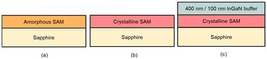
Figure 1.
Cross-sectional schematics of (a) amorphous SAM deposited with RF magnetron sputtering, (b) crystallization of the SAM by annealing in a tube furnace, (c) subsequent MOCVD growth of InGaN.
In the first set of experiments, the effect of pre-annealing sapphire was studied. The pre-annealing step improved the surface morphology and atomic step uniformity of the sapphire substrate [29,30]. Moreover, high-temperature treatment will result in a uniform oxygen-terminated surface that can improve the deposition of the SAM [31]. Pre-annealing of the sapphire substrate was performed at 1673 K for 10 h. A 40 nm thick amorphous SAM layer was deposited on the pre-annealed sapphire and unannealed sapphire. Both samples were then annealed for 10 h at 1173 K followed by 15 h at 1223 K for the layer crystallization. Further series of crystallization experiments were performed. The first was a time series where three samples with nominally the same amorphous SAM layer thickness of 75 nm were deposited on sapphire substrates. These samples were annealed at 1223 K for 20 h, 25 h, and 30 h. In the second set of crystallization experiments, three different thicknesses of the SAM layers were studied: 25 nm, 75 nm, and 90 nm. All the samples in the second series were annealed at 1223 K for 25 h. In the third series, the temperature of one of the two annealing steps was varied as follows. A thickness of 40 nm was chosen for two samples that were annealed for a total of 25 h at different temperatures for the first 10 h and 1223 K for the remaining 15 h. The second annealing step of 1223 K for 15 h was designed to ensure crystallization, and by varying the temperature of the first 10 h of annealing, the volumetric ratio of spinel to SAM phases was compared to determine the ideal crystallization annealing condition.
After SAM crystallization, InGaN layers were grown using MOCVD with triethylgallium (TEGa), trimethylindium (TMI), and ammonia (NH3). The 100 nm and 400 nm thick InGaN layers were grown with a calibrated composition of xIn = 0.14 on both SAM on sapphire as well as a reference GaN template on sapphire. These layers were grown with TMI and TEGa flows of 2.6 and 4.9 μmol min−1 at 1138K, respectively, with an NH3 flow of 89 mmol/min.
An atomic force microscopy (AFM) scan was performed to compare the surface morphology of the layers using a Bruker Icon AFM tool. The roughnesses of the films were evaluated and compared through the root-mean-square (RMS) Ra parameter. The thickness of the SAM layer was measured with X-ray reflectivity (XRR) using the Panalytical Empyrean X-ray diffractometer. The same equipment was utilized for ω−2θ and (ω−2θ)—ω reciprocal space map (RSM) scans to evaluate the film crystallinity as well as the layer composition. SAM- and spinel-phase MgAl2O4 peaks were identified with the indexes from previously reported structures [32,33]. The quality of the crystallized SAM layer was evaluated by comparing the spinel (311) to SAM (0009) peak-to-background intensity ratio, the SAM (0009) peak’s full width of half maximum range (FWHM), and the spinel (311) peak’s FWHM from the ω−2θ scans. Transmission electron microscope (TEM) studies are currently underway to investigate crystalline quality. Due to the thickness restriction on acquiring high-quality RSM on thin SAM films, RSM scans were performed on the reference InGaN on GaN template on sapphire to determine the calibrated indium content in 100 nm and 400 nm thick InGaN layers. The approximate indium content on different substrates was quantified with photoluminescence (PL) spectroscopy using a Horiba LabRAM HR Evolution Raman Spectrometer, using a blue 405 nm laser with an acquisition time of 0.5 s and 125 W/cm2 power. The systematic variation of the experimental parameters is summarized in Table 1. Sputtered amorphous SAM film on Si along with a bulk SAM substrate were externally characterized using X-ray fluorescence (XRF). XRF was performed using a Rigaku Primus II WDXRF X-ray source with a rhodium X-ray tube in vacuum conditions across a 10 mm diameter measurement area.

Table 1.
Phase content, ω−2θ FWHM, and roughness for crystallized SAM layers. The annealing temperature for part one (T1) and annealing time for part two (t2) were varied in different experiments. The time of annealing part one was 10 h (t1) and the temperature for annealing part two was 1223 K (T2).
3. Results and Discussions
3.1. XRF Results
The results of the film compositions (Wt%) and atomic percentages (At%) of sputtered amorphous SAM film on Si and bulk SAM substrate are summarized in Table 2. These results indicate that the stoichiometry of both the sputtered SAM film and the SAM substrate were fairly comparable, pointing to the possibility of using a crystalline thin SAM film as a substitute for SAM substrate.
Table 2.
Stoichiometry of amorphous SAM film on Si and SAM Substrate.
3.2. Effect of Pre-Annealing
The pre-annealing experiment was performed to improve the sapphire substrate morphology and study its effect on the crystallization of sputtered SAM.
Sample A and B (Table 1) have the same thickness (40 nm) with the same deposition and annealing condition (1173 K for 10 h and 1223 K for 15 h). Sample A used pre-annealed sapphire substrate and Sample B used unannealed sapphire substrate.
Sample A had a SAM reflection with a high peak-to-background ratio in the thin-layer XRD measurements (Figure 2a). Sample B remained amorphous or partially crystallized (Figure 2b). The surface roughness of A increased from 1.16 nm to 1.57 nm after crystallization, as shown in the (500 nm)2 size AFM scans (Figure 2d,c). Sample B showed an RMS roughness of 1 nm (Figure 2e) after annealing, which was similar to the RMS roughness of amorphous Sample A, 1.16 nm (Figure 2d). The crystalized samples tended to have a higher roughness than amorphous layers. As mentioned before, the pre-annealing step improved the surface morphology, and the oxygen-terminated surface aided the formation of crystalline SAM film above the sapphire substrate [29,30,31]. An improved substrate morphology of sapphire resulted in an efficient crystallization of Sample A compared to Sample B.
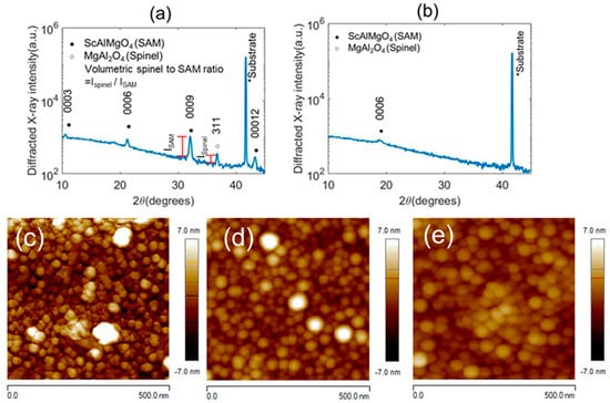
Figure 2.
X-ray diffraction ω–2θ scans of annealed SAM layer on (a) pre-annealed sapphire (Sample A) and (b) unannealed sapphire (Sample B). AFM images of (c) crystallized Sample A, with RMS roughness of 1.57 nm, (d) amorphous Sample A, with RMS roughness of 1.16 nm, and (e) Sample B (not fully crystallized), with RMS roughness of 1 nm.
3.3. Effect of SAM Thickness
Samples C, D, and E were deposited with thicknesses of 25 nm, 75 nm, and 90 nm, respectively, on a pre-annealed sapphire substrate. The crystallization for all three samples was conducted at 1223 K for 25 h. The results are compared using XRD and AFM (Table 1). As the thickness varied from 25 nm to 90 nm, the RMS roughness changed from 1.25 nm to 2.3 nm. The spinel-to-SAM ratio also increased from 0.203 to 0.408. The reason for this behavior could be that the spinel was crystallizing faster than SAM for a given thickness, and the higher the thickness of the layer, the longer the crystallization duration [34]. For thinner 25 nm SAM layers (Sample C), the spinel and SAM phase both crystallized for the annealing duration of 25 h, whereas for the 90 nm SAM layer (Sample E), the spinel phase crystallized; however, the SAM phase did not crystallize efficiently. The high spinel-to-SAM volumetric ratio resulted in the formation of facets, which increased the surface roughness, degrading the morphology. Increasing the layer thickness from 25 nm to 75 nm resulted in a decrease in the FWHM of the ω−2θ of the SAM 0009 reflection from 1188 to 900 arc-seconds, which then nominally remained the same from 75 nm to 90 nm thick SAM layers. This trend could be related to the interfacial reaction between SAM and sapphire during the annealing process resulting in a lower quality of the SAM layer near the interface [28]. With the increasing thickness of the SAM layer on sapphire, the contribution of this poor-quality interfacial layer on the peak intensity of the SAM layer in the XRD scan was reduced, resulting in a lower FWHM of the SAM layer.
3.4. Effect of Annealing Time
The effect of annealing at a fixed temperature (1123 K) for different durations was studied using 75 nm thick crystallized SAM on sapphire samples. Samples F, G, and H were annealed with durations of 20 h, 25 h, and 30 h, respectively. The RMS roughness increased from 1.41 nm to 2 nm with increasing annealing duration. The spinel-to-SAM volumetric ratio decreased from 0.453 to 0.177 with increasing duration. Although the spinel-to-SAM ratio decreased, the results are difficult to interpret due to the decrease in the overall intensity of both spinel (311) and SAM (0009) peaks, the reason for which is not well understood at this point. With a longer annealing duration, we speculate that the SAM crystallizes more effectively compared to a shorter annealing time due to a lower crystallization rate. The spinel-phase crystallization rate was faster than the SAM phase and the spinel X-ray reflections appeared with a relatively higher intensity than SAM when the sample was annealed for a shorter duration. Subsequent annealing steps resulted in the formation of more SAM-phase material, enhancing its relative intensity [34,35].
3.5. Effect of Annealing Temperature
A 25 h total annealing duration was chosen to proceed with the annealing temperature experiment. A high SAM thickness may increase the roughness of the film; however, an insufficient SAM thickness might fail to serve as a lattice-matched layer for the subsequently grown InGaN films. Thus, an intermediate-thickness 40 nm SAM layer was chosen in the following series, as surface roughness reduction was one of the main goals of this study. The temperature series was divided into a two-step annealing experiment for Samples A and I. The annealing temperature of the first 10 h was 1123 K (Sample A) and 1173 K (Sample I). In both cases, the first annealing step was followed by 15 h at 1223 K to ensure crystallization. Samples A and I were both pre-annealed and used the same thickness of SAM layer. After crystallization, Samples A and I had similar RMS roughness. Sample I had a slightly higher volumetric spinel-to-SAM ratio than Sample A, because the spinel phase may have formed at a faster rate compared to that of SAM at 1123 K (Table 1). The SAM may require a higher annealing temperature to crystallize sooner; however, beyond an optimized temperature, Sc-deficient regions may start to appear. More data points are required to determine a clear trend for the annealing temperature. The optimized crystallization temperature for SAM will be investigated in future work.
3.6. MOCVD Growth of Thick InGaN Layers
Samples F and H were placed in the MOCVD reactor to deposit a 100 nm thick InGaN layer. In addition, Samples G and I were utilized to deposit a 400 nm thick InGaN layer (Table 1). In both these experiments, reference GaN on sapphire templates were co-loaded to determine the indium content and InGaN relaxation extent on these samples with RSM (−1 −1 4) reflection scans. The SAM layers had low thickness compared with the sapphire substrate and the InGaN layer, resulting in a relatively low intensity in the XRD RSM scans. SAM was required as a reference for the lattice constant to measure the InGaN lattice constant and its relative degree of relaxation. However, the low intensity of SAM introduced challenges in obtaining high-resolution RSM measurements on InGaN on SAM on sapphire samples. RSM scans were performed on InGaN on GaN on sapphires samples and PL was performed on both samples to provide a quantitative comparison of the indium concentration between the InGaN on GaN template and the InGaN on SAM on sapphire. The grown structure included a targeted 3–5 nm of GaN interlayer to smooth the morphology, as reported in reference [36]. The corresponding ω–2θ diffraction patterns of the SAM Sample H before and after the MOCVD growth are shown in Figure 3a,b. The growth of the 100 nm InGaN layer on GaN on sapphire indicated the indium content of 0.145 with a degree of relaxation of 8.7%. The 400 nm thick layer showed two InGaN peaks: one corresponding to 14.2% indium content with a degree of relaxation of 15% and the second one with 14.9% indium content and a 67% degree of relaxation (Figure 3c,d). With a 400 nm InGaN thickness, the layer had exceeded its critical thickness on GaN on sapphire; hence, the second peak appeared with higher relaxation [37]. Both peaks of 400 nm InGaN had a higher degree of relaxation compared to the 100 nm InGaN layer owing to higher strain in the structure [38,39]. Comparing the surface morphology using RMS roughness for Samples F and H from Table 1, prior to the InGaN deposition, Sample H showed a significant reduction in the spinel-phase facets although with a slightly higher surface roughness, the reason for which is not well understood at this point (Table 1). However, Sample H demonstrated a lower spinel-to-SAM volumetric ratio of ~0.18 compared to ~0.45 for Sample F, which might be the reason for fewer formations of facets after the InGaN growth (Figure 4a,b). For the second MOCVD growth of the thicker 400 nm InGaN layer, prior to the MOCVD deposition, Samples G and I had a spinel-to-SAM volumetric ratio of ~0.45 and ~0.22, respectively. After the InGaN deposition, the AFM scan showed similar roughness for Samples G and I; however, Sample I showed a smaller grain size than Sample G, which we speculate may be due to the lower spinel-to-SAM volumetric ratio (Figure 4c,d). This suggests that further lowering of the spinel-to-SAM volumetric ratio is necessary to suppress the spinel facets in SAM and improve the homogeneity in the subsequently grown InGaN layer.
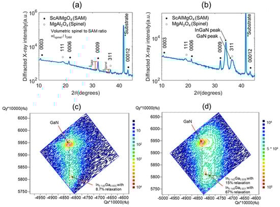
Figure 3.
→ XRD ω–2θ of (a) Sample H, (b) Sample H with 100 nm InGaN on 75 nm SAM layer on Al2O3; RSM (−1 −1 4) of (c) 100 nm InGaN on GaN template; RSM (−1 −1 4) of (d) 400 nm InGaN on GaN template.
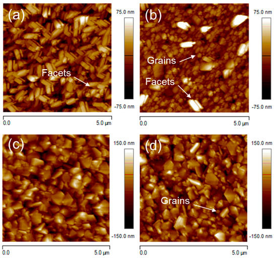
Figure 4.
AFM size 5 µm × 5 µm scan of (a) Sample F (100 nm InGaN layer), RMS roughness: 18.3 nm, (b) Sample H (100 nm InGaN layer), RMS roughness: 14.5 nm, (c) Sample G (400 nm InGaN layer), RMS roughness: 30.8 nm, (d) Sample I (400 nm) InGaN layer, RMS roughness: 31.3 nm.
The InGaN layer grown on SAM and GaN showed different PL wavelengths of emission (Figure 5a,b) suggesting different degrees of strain in the structure and different indium incorporation. Based on the strain information achieved from the RSM scans and PL emission wavelength, the indium compositions of InGaN on GaN on sapphire samples were estimated and compared to the indium composition measured in RSM scans for validation. Equations (1) and (2) were utilized [40,41], where Eg is the bandgap energy, R is the degree of relaxation, and x is the indium composition. The PL peak emission wavelength was converted to bandgap energy Eg using Equation (2) [41], where λ is the wavelength and is the photon energy, interpreted here as the bandgap energy of the InGaN layer. With this method, 100 nm InGaN on GaN on sapphire with a relaxation of 8% (from RSM) luminescing at 432 nm was determined to have an indium content of 14.5%, which is the same as the indium concentration measured with the XRD RSM scan shown in Figure 3c. However, the RSM scan of 400 nm InGaN on GaN on sapphire layer (Figure 3d), as discussed above, demonstrated two separate indium peaks, thereby making the indium content estimation challenging. Due to a ~10% larger lattice constant of InN compared to GaN [2], when thicker InGaN films are grown on GaN, the layer exceeds its critical thickness resulting in strain-relaxed films. The appearance of two separate peaks may be an indication of unintentionally relaxation-graded films, with a higher degree of relaxation for layers closer to the film surface, with RSM scans showing an averaged indium content and degree of relaxation across a range of thickness. Assuming the layers at the surface of the 400 nm thick InGaN on GaN on sapphire sample were 100 % relaxed, a luminescence at 475 nm as depicted in Figure 5b should have ~16 % indium content, using Equations (1) and (2), which is nominally similar to that observed from the two InGaN peaks in the Figure 3d RSM scan. As the PL characterization was performed on the top surface of the wafer, consideration of full relaxation of the films close to the surface to determine the indium content accurately can be justified.
Eg(R, x) = 3.42 + (0.69R + 3.42)x2 − (1.57R + 4.07)x.
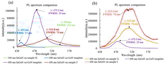
Figure 5.
PL spectrum of (a) 100 nm InGaN on SAM and GaN template with an intensity range of 0 to ~100,000. (b) 400 nm InGaN on SAM and GaN template with an intensity range of 0 to ~600,000 (400 nm InGaN on GaN template was the common spectrum for both plots).
For the InGaN on SAM on sapphire, as mentioned above, without a GaN buffer layer, utilization of a thin crystalline SAM layer posed challenges in acquiring the exact film composition and degree of relaxation with XRD RSM scans. Therefore, some assumptions were made for the degree of relaxation parameter to estimate the indium content using Equations (1) and (2) while using the PL wavelength as the only measured entity. For the InGaN on SAM on sapphire samples, applying 8.7% relaxation to Equation (1) to calculate the indium content of the 100 nm thick InGaN films for Samples F and H, the results were 32.7% and 46.1%, which are impractical. In addition, SAM films are lattice-matched to In0.17Ga0.83N [18,19,20]; therefore, these films can be considered as grown 100 % relaxed. Therefore, the indium composition of Samples F and H were recalculated considering full relaxation (R = 1 in Equation (1)), resulting in an indium composition of 20.8% for Sample F and 25.9% for Sample H. For the 400 nm thick InGaN on SAM on sapphire samples, Sample G and Sample I, the same assumption of 100% relaxation yielded indium concentrations of 20.8% and 20.9%, respectively.
The PL results of InGaN film on SAM on sapphire and the reference GaN on sapphire samples are summarized in Table 3. With a 100 nm InGaN layer grown on GaN on sapphire, a peak wavelength of 432 nm with a PL intensity of around 11,000 arbitrary units (a.u.) was measured, which will be considered as the baseline for comparison of the PL intensity of 100 nm InGaN samples grown on SAM. An increased thickness (400 nm) of the InGaN layer on GaN on sapphire depicted higher indium incorporation, thereby emitting a longer wavelength of 475 nm compared to 432 nm, with an improvement in the intensity (100,000 a.u) of almost ten times. The thick (400 nm) InGaN on GaN on sapphire was the second reference sample for the comparison with thick (400 nm) InGaN grown on SAM. Thick (400 nm) InGaN layer grown on 40 nm SAM (Sample I) produced a two times higher PL intensity, a 1.3 nm redshift in the peak emission wavelength, and a 6 nm lower FWHM compared to Sample G (75 nm of SAM), as shown in Figure 5b. This improvement in the PL emission characteristics could be due to the lower volumetric spinel-to-SAM ratio of Sample I (0.263) compared to Sample G (0.446). Although these two samples showed similar surface roughness measured with AFM, more small-sized grains were formed in Sample I whereas Sample G had larger facets, which might be the reason for the improved crystalline quality and lower FWHM of Sample I compared to Sample G (Figure 4c,d).
Table 3.
PL results of InGaN film on SAM on sapphire substrates along with reference InGaN on GaN on sapphire samples.
Although the PL emission of 400 nm InGaN on SAM on sapphire samples demonstrated a higher peak emission intensity, 100 nm InGaN grown on SAM showed a longer redshift, which is the intended target. The 100 nm InGaN layers on SAM on sapphire (Sample H) demonstrated the longest wavelength among all the samples with an indium composition of ~26%, but it also demonstrated a two times lower PL intensity compared with reference InGaN on GaN on sapphire (Figure 5a). Sample H was the only sample that demonstrated a lower intensity among all InGaN on SAM on sapphire samples compared with InGaN on GaN template. Further investigations are needed to understand this behavior. Comparing the 100 nm InGaN layers grown on SAM samples, Samples F (75 nm) and H (75 nm) emitted at different wavelengths with different intensities. While Sample F demonstrated a lower redshift of ~80 nm, a higher intensity of emission by approximately two times was observed, even with a poorer surface morphology. Owing to the higher indium incorporation, a drop in the emission intensity by half is still promising, considering the ~120 nm (555 nm compared to 432 nm) redshift for InGaN on Sample H compared to the GaN on sapphire. A more controlled experiment on Sample H needs to be performed to emit in the same range as Sample F to draw further conclusions about the lower emission intensity. The key difference between F and H was that Sample H had a lower spinel-to-SAM ratio and less formation of spinel facets (Figure 4a,b). The SAM samples with improved homogeneity result in an overall smoother surface morphology, critical for the subsequently grown InGaN layers. This PL result further strengthens our assertion that a lower spinel-to-SAM volumetric ratio is important to achieve high-quality InGaN layers on the optimized SAM on sapphire substrates that we have developed, but in this specific case it resulted in a higher indium content, thereby making the quality comparison inconclusive.
The FWHM of the PL for the InGaN on SAM layers was higher than that for the InGaN on GaN templates. This might be caused by the high surface roughness of the underlying SAM layers, resulting in a stronger indium surface segregation, which leads to a non-uniform indium incorporation [42]. The FWHM of the PL for the InGaN on SAM layers on sapphire obtained in our experiments were comparable to the InGaN layers grown on ZnO substrates [43]. Both thicknesses of the InGaN layers on the SAM on sapphire samples demonstrated higher intensities (two times higher for 100nm InGaN on Sample F and six times higher for 400 nm InGaN on Sample I) and longer emission wavelengths (around 123 nm for 100 nm InGaN and around 37 nm for 400 nm InGaN) than those grown on GaN on sapphire templates. Although the high surface roughness of the InGaN on SAM on sapphire samples may contribute to the increase in the PL intensity, it still cannot account for the high level of intensity enhancement observed in our experiments. Prior reports have shown that roughening of the surface on the nanometer scale has conventionally either degraded the PL intensity or led to minor enhancements [44,45]. However, when the surface roughness increased from the nanometer scale to the micrometer scale, the PL intensity was enhanced by almost twice. In our experiment, compared to InGaN on GaN on sapphire, the InGaN on SAM on sapphire samples had a surface roughness degradation on the scale of tens of nanometers, changing from ~30 nm to ~10 nm, respectively, for a 5 µm × 5 µm AFM scan. A two to six times higher PL intensity observed in this work, therefore, cannot be accounted for by this nanometer-scale change in surface roughness. Therefore, we speculate that the high InGaN material quality may be the reason for the higher PL intensity observed for the InGaN on SAM on sapphire samples.
This is one of the highest reported redshifts for any relaxed InGaN pseudo-substrate technology so far and one of the few wherein the redshift is accompanied by an increased emission intensity [21]. Further investigations will be pursued to achieve device results on these substrates. These results demonstrate the potential of SAM on sapphire substrates as a viable candidate to achieve thick, high-indium-concentration InGaN layers for long-wavelength emitters.
4. Conclusions
In this work, further optimization of SAM crystallization was investigated to suppress the spinel phase to obtain an improved surface morphology. Compared to the previous work [28], both the surface roughness and the volumetric ratio of the spinel to SAM phase have improved. From the thick InGaN layer growth, we identified that the spinel-to-SAM ratio was one of the key parameters to suppress spinel-phase facets that transfer onto the MOCVD-grown layer surface, increasing the overall surface roughness value. The higher PL intensity along with the redshift demonstration of the InGaN layers on SAM demonstrate the potential of sputtered and crystallized SAM as a promising substrate for longer-wavelength III-nitride emitters. The growth condition for the InGaN layers was not extensively optimized in this work. In the future, we will further investigate the optimized annealing temperature for SAM crystallization and design better growth conditions for the epitaxial growth of InGaN on SAM to grow the light-emitter structures.
Author Contributions
Investigation, G.W., S.S.P. and P.G.E.; Formal analysis, G.W. and Y.L.; Data curation, G.W., Y.L., J.K., Y.H. and J.C.; Methodology, G.W., Y.L., J.K., S.M. (Samuel Marks), R.L., C.L., S.S.P. and P.G.E.; Visualization, G.W.; Writing—original draft, G.W.; Writing—review and editing, G.W., S.M. (Swarnav Mukhopadhyay), S.S.P. and P.G.E.; Project administration, S.S.P. and P.G.E.; Supervision, S.S.P. and P.G.E.; Validation, S.S.P. and P.G.E.; Funding acquisition, S.S.P. All authors have read and agreed to the published version of the manuscript.
Funding
This work was financially supported by the National Science Foundation Materials Research Science and Engineering Center (DMR-1720415).
Institutional Review Board Statement
Not applicable.
Informed Consent Statement
Not applicable.
Data Availability Statement
The data that support the findings of this study are available from the corresponding author upon reasonable request.
Acknowledgments
We would like to thank Brandon Erickson for helping with manuscript proofreading. The authors gratefully acknowledge the use of facilities and instrumentation supported by NSF through the University of Wisconsin Materials Research Science and Engineering Center (DMR-1720415).
Conflicts of Interest
The authors declare that they have no conflict of interest.
References
- Kour, R.; Arya, S.; Verma, S.; Singh, A.; Mahajan, P.; Khosla, A. Review—Recent Advances and Challenges in Indium Gallium Nitride (In x Ga 1-x N) Materials for Solid State Lighting. ECS J. Solid State Sci. Technol. 2020, 9, 015011. [Google Scholar] [CrossRef]
- Rinke, P.; Scheffler, M.; Qteish, A.; Winkelnkemper, M.; Bimberg, D.; Neugebauer, J. Band Gap and Band Parameters of InN and GaN from Quasiparticle Energy Calculations Based on Exact-Exchange Density-Functional Theory. Appl. Phys. Lett. 2006, 89, 161919. [Google Scholar] [CrossRef]
- Yamaguchi, S.; Kariya, M.; Nitta, S.; Takeuchi, T.; Wetzel, C.; Amano, H.; Akasaki, I. Structural Properties of InN on GaN Grown by Metalorganic Vapor-Phase Epitaxy. J. Appl. Phys. 1999, 85, 7682–7688. [Google Scholar] [CrossRef]
- Kim, Y.H.; Park, H.J.; Kim, K.; Kim, C.S.; Yun, W.S.; Lee, J.W.; Kim, M.D. Strain Distribution and Interface Modulation of Highly Lattice-Mismatched InN/GaN Heterostructure Nanowires. Appl. Phys. Lett. 2009, 95, 033112. [Google Scholar] [CrossRef]
- Matsuoka, T. Progress in Nitride Semiconductors from GaN to InN—MOVPE Growth and Characteristics. Superlattices Microstruct. 2005, 37, 19–32. [Google Scholar] [CrossRef]
- Tan, A.K.; Hamzah, N.A.; Ahmad, M.A.; Ng, S.S.; Hassan, Z. Recent Advances and Challenges in the MOCVD Growth of Indium Gallium Nitride: A Brief Review. Mater. Sci. Semicond. Process. 2022, 143, 106545. [Google Scholar] [CrossRef]
- Fan, K.; Tao, J.; Zhao, Y.; Li, P.; Sun, W.; Zhu, L.; Lv, J.; Qin, Y.; Wang, Q.; Liang, J.; et al. Size Effects of AlGaInP Red Vertical Micro-LEDs on Silicon Substrate. Results Phys. 2022, 36, 105449. [Google Scholar] [CrossRef]
- Wong, M.S.; Kearns, J.A.; Lee, C.; Smith, J.M.; Lynsky, C.; Lheureux, G.; Choi, H.; Kim, J.; Kim, C.; Nakamura, S.; et al. Improved Performance of AlGaInP Red Micro-Light-Emitting Diodes with Sidewall Treatments. Opt. Express 2020, 28, 5787–5793. [Google Scholar] [CrossRef]
- Oh, J.-T.; Lee, S.-Y.; Moon, Y.-T.; Moon, J.H.; Park, S.; Hong, K.Y.; Song, K.Y.; Oh, C.; Shim, J.-I.; Jeong, H.-H.; et al. Light Output Performance of Red AlGaInP-Based Light Emitting Diodes with Different Chip Geometries and Structures. Opt. Express 2018, 26, 11194–11200. [Google Scholar] [CrossRef]
- Wasisto, H.S.; Prades, J.D.; Gülink, J.; Waag, A. Beyond Solid-State Lighting: Miniaturization, Hybrid Integration, and Applications of GaN Nano- and Micro-LEDs. Appl. Phys. Rev. 2019, 6, 041315. [Google Scholar] [CrossRef]
- Horng, R.-H.; Ye, C.-X.; Chen, P.-W.; Iida, D.; Ohkawa, K.; Wu, Y.-R.; Wuu, D.-S. Study on the Effect of Size on InGaN Red Micro-LEDs. Sci. Rep. 2022, 12, 1324. [Google Scholar] [CrossRef] [PubMed]
- Huang, Y.-M.; Peng, C.-Y.; Miao, W.-C.; Chiang, H.; Lee, T.-Y.; Chang, Y.-H.; Singh, K.J.; Iida, Z.D.; Horng, R.-H.; Chow, C.-W.; et al. High-Efficiency InGaN Red Micro-LEDs for Visible Light Communication. Photon. Res. 2022, 10, 1978–1986. [Google Scholar] [CrossRef]
- Matsuoka, T.; Yoshimoto, N.; Sasaki, T.; Katsui, A. Wide-Gap Semiconductor InGaN and InGaAln Grown by MOVPE. J. Electron. Mater. 1992, 21, 157–163. [Google Scholar] [CrossRef]
- Wang, S.-J.; Li, N.; Park, E.-H.; Feng, Z.C.; Valencia, A.; Nause, J.; Kane, M.; Summers, C.; Ferguson, I. MOCVD Growth of GaN-Based Materials on ZnO Substrates. Phys. Status Solidi C 2008, 5, 1736–1739. [Google Scholar] [CrossRef]
- Lei, Y.; Xu, J.; Zhu, K.; He, M.; Zhou, J.; Gao, Y.; Zhang, L.; Chen, Y. A GaN-Based LED With Perpendicular Structure Fabricated on a ZnO Substrate by MOCVD. J. Display Technol. 2013, 9, 377–381. [Google Scholar] [CrossRef]
- Wang, S.-J.; Li, N.; Park, E.-H.; Lien, S.-C.; Feng, Z.C.; Valencia, A.; Nause, J.; Ferguson, I. Metalorganic Chemical Vapor Deposition of InGaN Layers on ZnO Substrates. J. Appl. Phys. 2007, 102, 106105. [Google Scholar] [CrossRef]
- Li, N.; Wang, S.-J.; Huang, C.-L.; Feng, Z.C.; Valencia, A.; Nause, J.; Summers, C.; Ferguson, I. Effect of an Al2O3 Transition Layer on InGaN on ZnO Substrates by Organometallic Vapor-Phase Epitaxy. J. Cryst. Growth 2008, 310, 4908–4912. [Google Scholar] [CrossRef]
- Ozaki, T.; Takagi, Y.; Nishinaka, J.; Funato, M.; Kawakami, Y. Metalorganic Vapor Phase Epitaxy of GaN and Lattice-Matched InGaN on ScAlMgO4(0001) Substrates. Appl. Phys. Express 2014, 7, 091001. [Google Scholar] [CrossRef]
- Ozaki, T.; Funato, M.; Kawakami, Y. InGaN-Based Visible Light-Emitting Diodes on ScAlMgO4(0001) Substrates. Appl. Phys. Express 2015, 8, 062101. [Google Scholar] [CrossRef]
- Takahashi, R.; Fujiki, R.; Hozo, K.; Hiramatsu, R.; Matsukura, M.; Kojima, T.; Han, D.-P.; Iwaya, M.; Takeuchi, T.; Kamiyama, S. Improvement of 650-Nm Red-Emitting GaIn0.17N/GaIn0.38N Multiple Quantum Wells on ScAlMgO4 (0001) Substrate by Suppressing Impurity Diffusion/Penetration. Appl. Phys. Lett. 2022, 120, 142102. [Google Scholar] [CrossRef]
- Pasayat, S.S.; Gupta, C.; Wong, M.S.; Wang, Y.; Nakamura, S.; Denbaars, S.P.; Keller, S.; Mishra, U.K. Growth of Strain-Relaxed InGaN on Micrometer-Sized Patterned Compliant GaN Pseudo-Substrates. Appl. Phys. Lett. 2020, 116, 111101. [Google Scholar] [CrossRef]
- Mynbaeva, M.; Titkov, A.; Kryganovskii, A.; Ratnikov, V.; Mynbaev, K.; Huhtinen, H.; Laiho, R.; Dmitriev, V. Structural Characterization and Strain Relaxation in Porous GaN Layers. Appl. Phys. Lett. 2000, 76, 1113–1115. [Google Scholar] [CrossRef]
- Pasayat, S.S.; Gupta, C.; Acker-James, D.; Cohen, D.A.; DenBaars, S.P.; Nakamura, S.; Keller, S.; Mishra, U.K.; Fellow, I. Fabrication of Relaxed InGaN Pseudo-Substrates Composed of Micron-Sized Pattern Arrays with High Fill Factors Using Porous GaN. Semicond. Sci. Technol. 2019, 34, 115020. [Google Scholar] [CrossRef]
- Pasayat, S.S.; Gupta, C.; Wong, M.S.; Ley, R.; Gordon, M.J.; DenBaars, S.P.; Nakamura, S.; Keller, S.; Mishra, U.K. Demonstration of Ultra-Small (<10 µm) 632 nm Red InGaN Micro-LEDs with Useful on-Wafer External Quantum Efficiency (>0.2%) for Mini-Displays. Appl. Phys. Express 2020, 14, 011004. [Google Scholar]
- Chan, P.; DenBaars, S.P.; Nakamura, S. Growth of Highly Relaxed InGaN Pseudo-Substrates over Full 2-in. Wafers. Appl. Phys. Lett. 2021, 119, 131106. [Google Scholar] [CrossRef]
- Chan, P.; Rienzi, V.; Lim, N.; Chang, H.-M.; Gordon, M.; DenBaars, S.P.; Nakamura, S. Demonstration of Relaxed InGaN-Based Red LEDs Grown with High Active Region Temperature. Appl. Phys. Express 2021, 14, 101002. [Google Scholar] [CrossRef]
- Quote from Aemdeposition. Available online: www.aemdeposition.com (accessed on 5 July 2022).
- Chen, Y.; Zuo, P.; Guan, Y.; Yusuf, M.H.; Babcock, S.E.; Kuech, T.F.; Evans, P.G. Reduction of Interface Reactions in the Low-Temperature Solid-Phase Epitaxy of ScAlMgO4 on Al2O3(0001). Cryst. Growth Des. 2020, 20, 6001–6007. [Google Scholar] [CrossRef]
- Yoshimoto, M.; Maeda, T.; Ohnishi, T.; Koinuma, H.; Ishiyama, O.; Shinohara, M.; Kubo, M.; Miura, R.; Miyamoto, A. Atomic-scale Formation of Ultrasmooth Surfaces on Sapphire Substrates for High-quality Thin-film Fabrication. Appl. Phys. Lett. 1995, 67, 2615–2617. [Google Scholar] [CrossRef]
- Shan, J.; Sun, J.; Liu, Z. Chemical Vapor Deposition Synthesis of Graphene over Sapphire Substrates. ChemNanoMat 2021, 7, 515–525. [Google Scholar] [CrossRef]
- Tsuda, M.; Watanabe, K.; Kamiyama, S.; Amano, H.; Akasaki, I.; Liu, R.; Bell, A.; Ponce, F.A. Mechanism of H2 Pre-Annealing on the Growth of GaN on Sapphire by MOVPE. Appl. Surf. Sci. 2003, 216, 585–589. [Google Scholar] [CrossRef]
- Kimizuka, N.; Mohri, T. Structural Classification of RAO3(MO)n Compounds (R = Sc, In, Y, or Lanthanides; A = Fe(III), Ga, Cr, or Al; M = Divalent Cation; n = 1−11). J. Solid State Chem. 1989, 78, 98–107. [Google Scholar] [CrossRef]
- Zorina, N.G.; Kvitka, S.S. Refinement of the Structure of the Spinel Al2MgO4. Sov. Phys. Crystallogr. 1969, 13, 599–600. [Google Scholar]
- Mani, G.K.; Rayappan, J.B.B. Impact of Annealing Duration on Spray Pyrolysis Deposited Nanostructured Zinc Oxide Thin Films. Superlattices Microstruct. 2014, 67, 82–87. [Google Scholar] [CrossRef]
- Kužel, R.; Nichtová, L.; Matěj, Z.; Musil, J. In-Situ X-Ray Diffraction Studies of Time and Thickness Dependence of Crystallization of Amorphous TiO2 Thin Films and Stress Evolution. Thin Solid Film. 2010, 519, 1649–1654. [Google Scholar] [CrossRef]
- White, R.C.; Khoury, M.; Wu, F.; Keller, S.; Rozhavskaia, M.; Sotta, D.; Nakamura, S.; DenBaars, S.P. MOCVD Growth of Thick V-Pit-Free InGaN Films on Semi-Relaxed InGaN Substrates. Semicond. Sci. Technol. 2021, 36, 015011. [Google Scholar]
- Holec, D.; Costa, P.M.F.J.; Kappers, M.J.; Humphreys, C.J. Critical Thickness Calculations for InGaN/GaN. J. Cryst. Growth 2007, 303, 314–317. [Google Scholar] [CrossRef]
- Chaudhuri, R.; Zhang, Z.; Xing, H.G.; Jena, D. Very High Density (>1014 cm−2 ) Polarization-Induced 2D Hole Gases Observed in Undoped Pseudomorphic InGaN/AlN Heterostructures. Adv. Elect. Mater. 2022, 8, 2101120. [Google Scholar] [CrossRef]
- Pasayat, S.S.; Gupta, C.; Wang, Y.; DenBaars, S.P.; Nakamura, S.; Keller, S.; Mishra, U.K. Compliant Micron-Sized Patterned InGaN Pseudo-Substrates Utilizing Porous GaN. Materials 2020, 13, 213. [Google Scholar] [CrossRef]
- Parker, C.A.; Roberts, J.C.; Bedair, S.M.; Reed, M.J.; Liu, S.X.; El-Masry, N.A.; Robins, L.H. Optical Band Gap Dependence on Composition and Thickness of InxGa1−xN. Appl. Phys. Lett. 1999, 75, 2566–2568. [Google Scholar] [CrossRef]
- Soga, T. Chapter 1-Fundamentals of Solar Cell. In Nanostructured Materials for Solar Energy Conversion; Soga, T., Ed.; Elsevier: Amsterdam, The Netherlands, 2006; pp. 3–43. [Google Scholar]
- Chen, H.; Feenstra, R.M.; Northrup, J.E.; Neugebauer, J.; Greve, D.W. Indium Incorporation and Surface Segregation during InGaN Growth by Molecular Beam Epitaxy: Experiment and Theory. MRS Internet J. Nitride Semicond. Res. 2001, 6, e11. [Google Scholar] [CrossRef]
- Khan, K.; Biswas, M.; Ahmadi, E. Growth of High Quality (In,Ga)N Films on O-Face ZnO Substrates by Plasma-Assisted Molecular Beam Epitaxy. AIP Adv. 2020, 10, 075120. [Google Scholar] [CrossRef]
- Wagner, A.; Ratzker, B.; Kalabukhov, S.; Frage, N. Enhanced External Luminescence Quantum Efficiency of Ceramic Phosphors by Surface Roughening. J. Lumin. 2019, 213, 454–458. [Google Scholar] [CrossRef]
- López, J.; Morales, A.; Aceves, M.; Yu, Z.; Domínguez, C. Analysis of Surface Roughness and Its Relationship with Photoluminescence Properties of Silicon-Rich Oxide Films. J. Vac. Sci. Technol. A Vac. Surf. Film. 2008, 27, 57. [Google Scholar] [CrossRef]


Disclaimer/Publisher’s Note: The statements, opinions and data contained in all publications are solely those of the individual author(s) and contributor(s) and not of MDPI and/or the editor(s). MDPI and/or the editor(s) disclaim responsibility for any injury to people or property resulting from any ideas, methods, instructions or products referred to in the content. |
© 2023 by the authors. Licensee MDPI, Basel, Switzerland. This article is an open access article distributed under the terms and conditions of the Creative Commons Attribution (CC BY) license (https://creativecommons.org/licenses/by/4.0/).