


Abstract
Effective terahertz (THz) modulation remains a critical challenge for advancing THz technology. Recently, two-dimensional (2D) materials integrated with high-resistance silicon (Si) have emerged as promising heterojunction platforms for THz control. In this paper, we experimentally demonstrate an all-optically controlled THz modulator based on a large-area WSe2/Si heterojunction, fabricated by magnetron sputtering of tungsten on Si followed by vacuum selenization. The device exhibits broadband modulation across 0.1–1.1 THz, achieving a modulation depth of 72% at a pump power of 1500 mW/cm2, significantly higher than that of bare Si or pristine WSe2 films. Moreover, we systematically analyze the underlying mechanism responsible for this enhanced performance. This study presents an effective and scalable strategy for THz modulation using 2D material/Si heterojunctions.
1. Introduction
Terahertz (THz) waves have garnered considerable interest due to their unique advantages in medical imaging [1,2], communications [3], sensing [4], molecular spectroscopy [5,6,7], and other promising applications. Although significant progress has been made in THz generators and detectors, the development of functional devices, especially modulators, remains a bottleneck [6]. THz modulators, which enable dynamic control over amplitude, phase, and polarization [8], have been realized using diverse materials [7,9,10,11,12,13,14,15,16,17]. However, most existing designs suffer from high insertion losses, stringent operating requirements, and limited modulation range, hindering practical deployments and applications. As THz technology matures, there is a growing demand for modulators with higher modulation depth and broader bandwidth [18].
Current THz modulation strategies rely primarily on optical, electrical, or thermal stimuli [19]. Among these, all-optical modulation excels in both modulation depth and speed, positioning heterojunction-based all-optical THz modulators as a promising avenue [20]. In this context, two-dimensional (2D) materials have emerged as attractive candidates owing to their excellent optoelectronic properties. Compared with conventional semiconductors, 2D materials offer higher carrier mobility and shorter relaxation times, which are critical parameters for device performance [21]. For example, Weis et al. first demonstrated high-efficiency THz modulation in graphene under femtosecond laser pumping [22]. Subsequently, Wen et al. proposed optically active graphene-on-germanium modulators [23]. Nevertheless, graphene’s intrinsic zero bandgap restricts its further development in the THz applications. Transition metal dichalcogenides (TMDCs), with bandgaps of 1–3 eV, overcome this limitation and hold great promise for THz devices [24,25]. Moreover, TMDCs can form type-II heterojunctions with traditional semiconductors, alleviating the weak light absorption inherent to their atomic-scale thickness [26,27]. For instance, Chen et al. first reported a MoS2/Si heterostructure THz modulator grown via chemical vapor deposition (CVD) [8]. Subsequently, Cao et al. improved the modulation depth of similar devices through annealing [28]. To further enhance modulation depth, Zheng et al. introduced an optically pumped MoS2-Si heterostructure metasurface THz modulator with monolayer MoS2 grown by high-pressure CVD [29]. Additionally, Qiao et al. demonstrated a high-performance MoTe2/Si all-optically controlled THz modulator fabricated by spin-coating [30]. Alka Jakhar et al. fabricated a PtSe2/Si-based THz modulator using a combination strategy of both CVD and physical vapor deposition (PVD) methods [31]. Lv et al. developed a broadband THz modulator based on an optically controlled GeSe2/Si heterojunction via magnetron sputtering and vacuum selenization [32]. Despite these advances, current THz modulators still face key challenges, including the fabrication of large-area continuous films and low modulation depth, which severely hinder practical applications [33,34].
Among TMDCs, WSe2 is particularly attractive for THz modulation due to its direct bandgap, enabling efficient photoexcitation and strong light–matter interaction [25]. More importantly, WSe2 forms a type-II heterojunction with Si, featuring conduction- and valence-band offsets of ~0.05 eV and ~0.13 eV, respectively [35]. This alignment promotes efficient spatial separation of photogenerated electron-hole pairs at the interface, suppressing carrier recombination and prolonging carrier lifetime, and thus enhancing photoconductivity and modulation depth. These interface-induced benefits are directly evidenced by time-resolved THz emission spectroscopy, which reveals that the built-in electric field accelerates carrier migration and amplifies photocurrent by nearly an order of magnitude [36]. Compared with MoS2 (indirect bandgap ~1.29 eV) and MoTe2 (narrower bandgap ~1.0 eV), WSe2 offers superior band alignment with Si and stronger valley-spin coupling, favorable for photocarrier manipulation. Previous experiments have confirmed that monolayer WSe2 on Si increases THz modulation depth by approximately 40% relative to bare Si [37]. From a fabrication standpoint, magnetron sputtering followed by vacuum selenization yields large-area, continuous, highly crystalline WSe2 films with excellent uniformity, compatible with standard semiconductor processing for scalable production [38]. These combined merits motivate our development of a WSe2/Si heterojunction-based THz modulator.
In this paper, we demonstrate an optically controlled THz modulator based on a large-area WSe2/Si heterojunction fabricated by magnetron sputtering followed by vacuum selenization. Under 850 nm continuous-wave (CW) laser pumping at 1500 mW/cm2, the device exhibits a broadband response from 0.1 to 1.1 THz and achieves a maximum modulation depth of 72% at 0.5 THz, significantly outperforming bare Si, single WSe2 structures, and graphene-based modulators. Therefore, this work provides a feasible pathway for large-area 2D TMDC-based THz modulation.
2. Preparation and Characterization
2.1. Fabrication of WSe2/Si Heterojunction
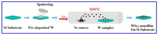
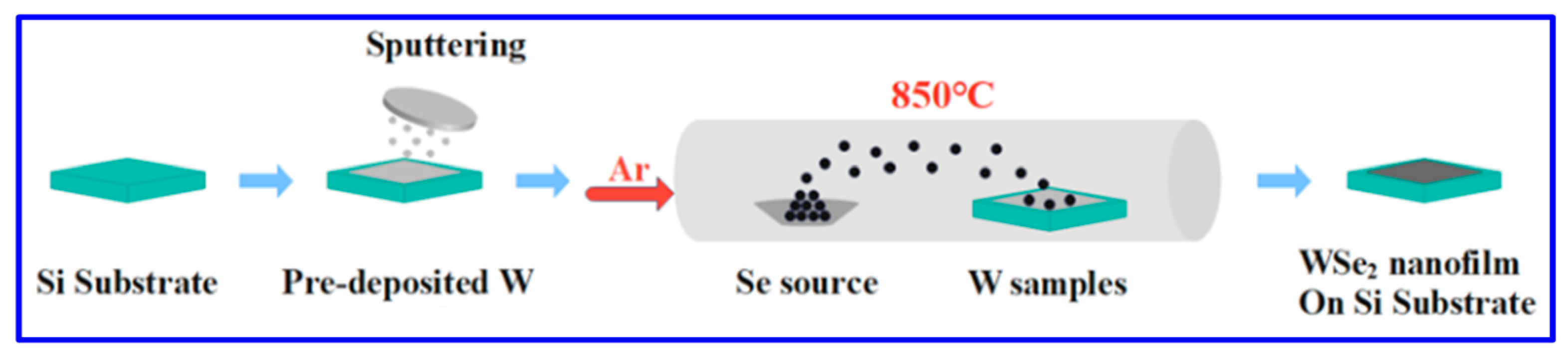
WSe2/Si heterojunction was fabricated via a two-step process, as illustrated in Figure 1. First, tungsten (W) films were deposited onto a single-side-polished 500 μm-thick high-resistance Si substrate (110) by magnetron sputtering. Prior to deposition, the substrates were cleaned with ethanol and deionized water. The sputtering parameters for the tungsten film are summarized in Table 1. Subsequently, the as-deposited W film and high-purity selenium (Se) powder (99.99%) were sealed in an evacuated quartz tube and heated to 850 °C at a ramp rate of 5 °C min−1 for 3 h to promote selenization according to W + 2Se → WSe2. To prevent oxidation, Ar gas (30 sccm) was introduced into the tube throughout the reaction. After selenization, the sample was naturally cooled to room temperature inside the tube furnace before removal. Detailed reaction parameters are listed in Table 2.
Figure 1.
Preparation flow of the WSe2/Si heterojunction.
Table 1.
Parameters of magnetron sputtering.
Table 2.
Parameters of selenization reaction.
2.2. Characterization of WSe2/Si Heterojunction
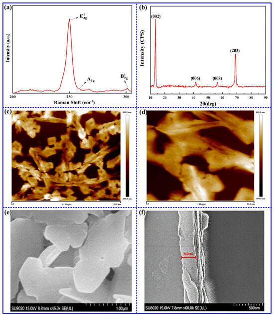
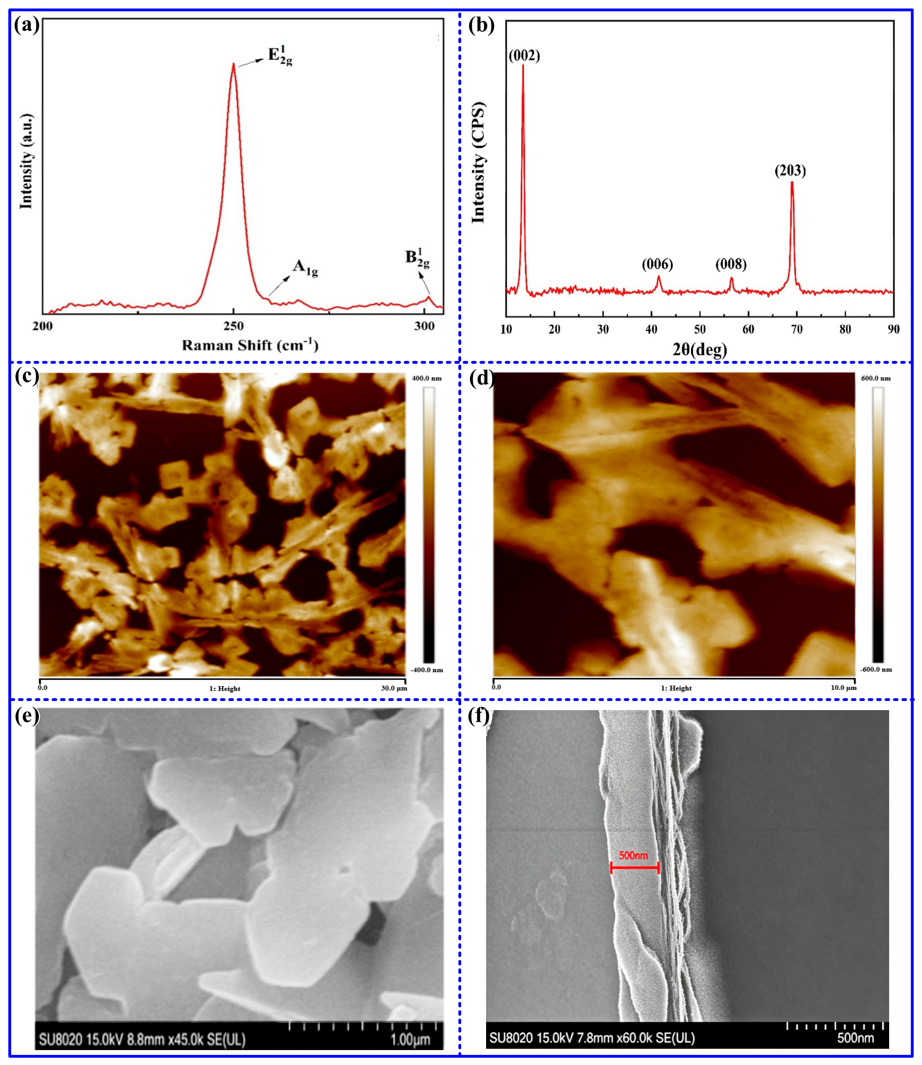
The as-prepared WSe2/Si heterojunction was systematically characterized by Raman spectroscopy, X-ray diffraction (XRD), atomic force microscopy (AFM), and scanning electron microscopy (SEM), as shown in Figure 2. Raman spectrum (Figure 2a) reveals a prominent peak at approximately 250 cm−1, assigned to the mode characteristic of few-layer WSe2. The XRD pattern (Figure 2b) exhibits sharp diffraction peaks indexed to the (002), (006), (008), and (203) planes, confirming a highly c-axis-oriented WSe2 film with good crystallinity and no detectable secondary orientations. AFM topography was acquired in tapping mode over scan areas of 30 μm × 30 μm and 10 μm × 10 μm (Figure 2c,d). Raw data were processed only with standard flattening routines to remove background tilt. The AFM images reveal a pinhole-rich surface with unevenly distributed WSe2. SEM micrographs, obtained at 15 kV, show densely packed WSe2 grains larger than 1 μm with multidirectional growth in plan-view (Figure 2e), while the cross-sectional view indicates a uniform film thickness of approximately 500 nm (Figure 2f). Collectively, these results confirm the successful growth of a dense, highly crystalline, and well-adhered WSe2 film on Si via magnetron sputtering followed by selenization, providing a solid foundation for the THz modulation studies presented below.
Figure 2.
Characterization of the fabricated WSe2/Si samples: (a) Raman spectrum, (b) XRD pattern, (c) AFM image (30 μm scale), (d) AFM image (10 μm scale), (e) SEM surface image, and (f) cross-sectional SEM image.
3. Results and Discussion
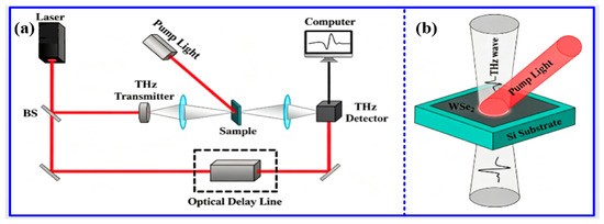
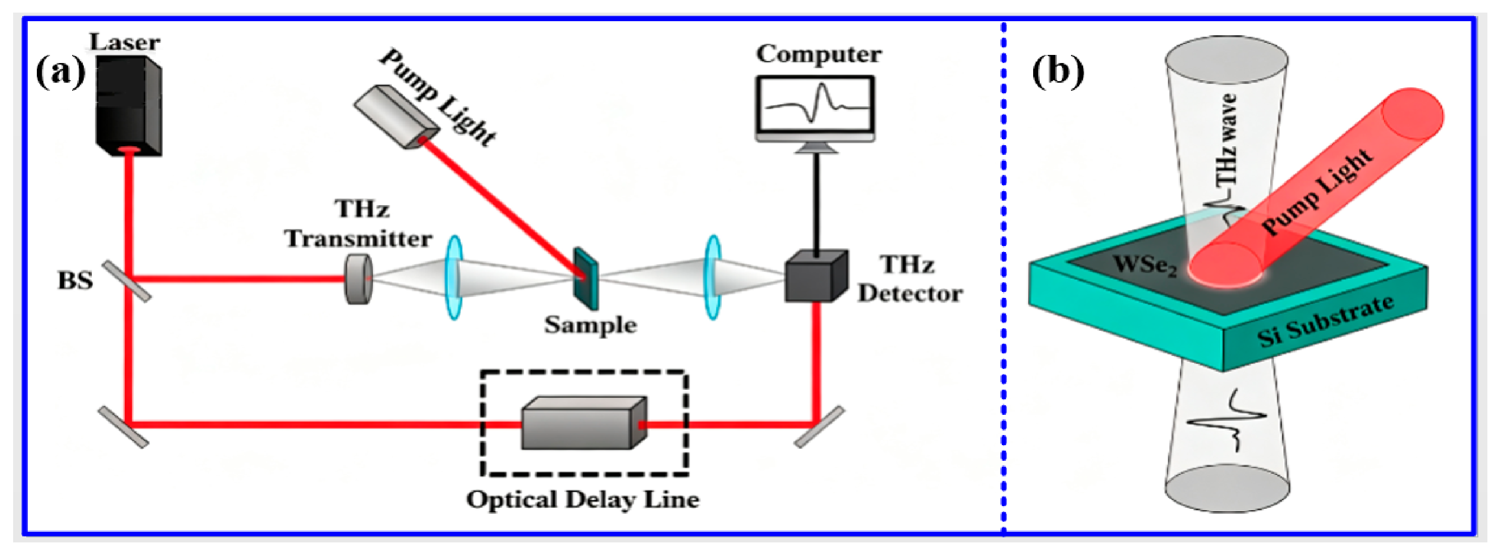
The THz modulation performance of the WSe2/Si heterojunction was characterized using a home-built THz time-domain spectroscopy (THz-TDS) system based on asynchronous optical sampling, as schematically shown in Figure 3a. The system employs a MaiTai SP femtosecond laser (90 fs pulse duration, 800 nm center wavelength, and 1 kHz repetition rate) as the source, with photoconductive antennas for THz generation and detection, a delay stage, and a lock-in amplifier. The emitted THz beam is collected and collimated by four off-axis parabolic mirrors. An 850 nm CW laser serves as the pump source to enable efficient interband absorption, as its photon energy exceeds the bandgaps of both WSe2 and Si [39]. The pump spot is carefully aligned to fully overlap with the THz beam on the modulator surface (Figure 3b). Since the pump is a CW source, it does not generate impulsive THz emission via optical rectification or transient photocurrent. Instead, it merely establishes a quasi-static photogenerated carrier distribution that modifies the complex conductivity and attenuates the transmitted THz probe pulse. Any incoherent steady-state background from the CW pump lies outside the THz range or is suppressed by the lock-in amplifier synchronized to the probe beam modulation. Furthermore, the absence of synchronous pump-probe delay gating ensures that any residual emits. Thus, the observed modulation purely reflects the pump-induced conductivity change, free from spurious THz emission or background artifacts.
Figure 3.
THz characterization of the prepared modulator: (a) schematic diagram of the THz-TDS system integrated with an 850 nm CW laser source and (b) schematic of the WSe2/Si heterojunction THz modulator.
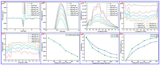
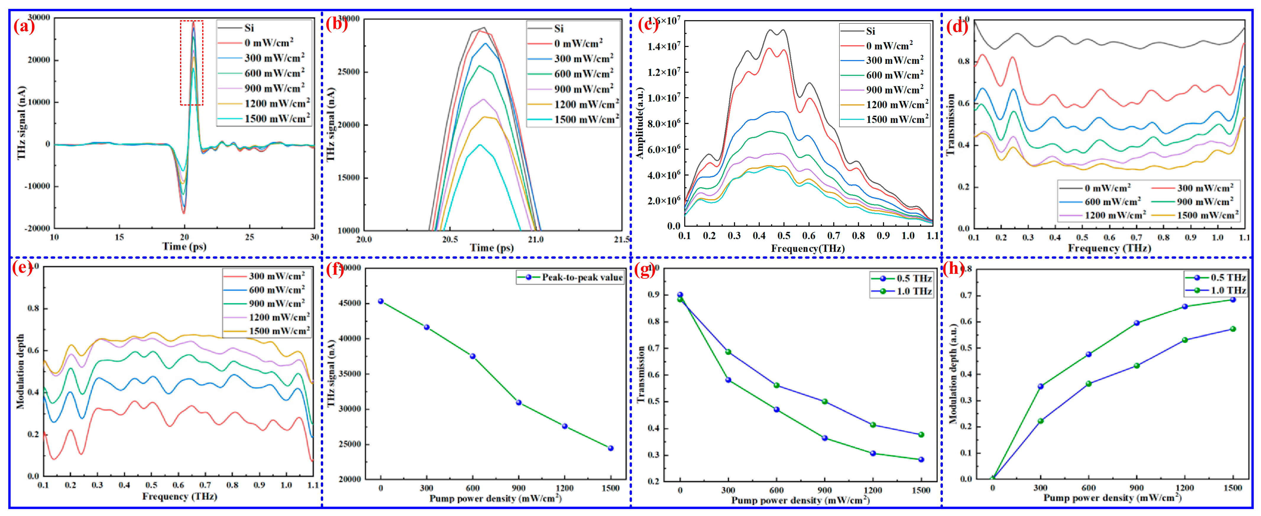
Figure 4a presents the time-domain THz transmission signals of the WSe2/Si heterojunction modulator with and without pump irradiation, using the bare Si substrate as a reference (not free space). Although the 500-μm Si wafer introduces a bulk delay of several picoseconds relative to air, this delay is identical for the reference and sample and cancels out in direct comparison. Without pumping, a slight amplitude attenuation and a negligible time shift (<0.05 ps, within the system jitter and experimental resolution) are observed between the heterojunction and the bare Si reference (Figure 4b, confirming that the 500 nm WSe2 overlayer introduces no appreciable phase lag. Therefore, this combination of small attenuation and the negligible delay unequivocally substantiates the successful formation of the WSe2 thin film on Si. As the pump power increases from 0 to 1500 mW/cm2, the THz amplitude decreases monotonically, indicating a clear pump-power-dependent conductivity modulation. The corresponding frequency-domain spectra, obtained by fast Fourier transform of the time-domain waveforms, show consistent trends (Figure 4c). To avoid numerical artifacts, all time-domain signals were zero-padded and multiplied by a symmetric window function with identical parameters, ensuring reliable relative comparisons. To further quantify the frequency-dependent behavior, normalized transmission spectra were extracted using:
where and are the Fourier transforms of the reference and sample time-domain signals, and and are the amplitude and phase of transmission coefficients. Figure 4d displays the normalized transmission spectra from 0.1 to 1.1 THz under various pump powers. Without excitation, THz waves readily penetrate the modulator. As the pump power increases, the normalized transmission intensity decreases markedly across the entire frequency range, indicating a broadband modulation. For instance, the average normalized transmission drops from 0.92 to 0.28 over 0.1–1.1 THz as the pump power increases from 0 to 1200 mW/cm2. At 1500 mW/cm2, the attenuation approaches saturation, enabling maximum modulation. This attenuation is attributed to THz absorption and reflection by photogenerated carriers [40,41].
Figure 4.
Transmission performance of the WSe2/Si heterojunction THz modulator: (a) time-domain spectra, (b) frequency-domain spectra, (c) modulation depth, (d) peak-to-peak values versus pump power, (e) transmission intensities at 0.5 and 1.0 THz versus different pump powers, and (f) modulation depths at 0.5 and 1.0 THz versus different pump powers. (g) Normalized transmission intensity versus pump power at 0.5 and 1.0 THz. (h) Modulation depth (MD) versus pump power at the same frequencies.
To quantify the modulation performance, the modulation depth (MD) is defined as [42]:
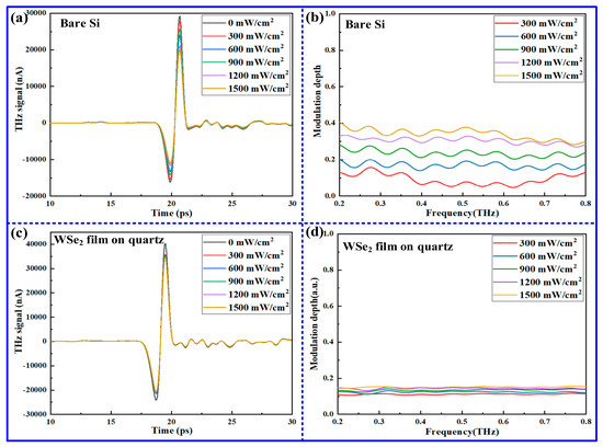
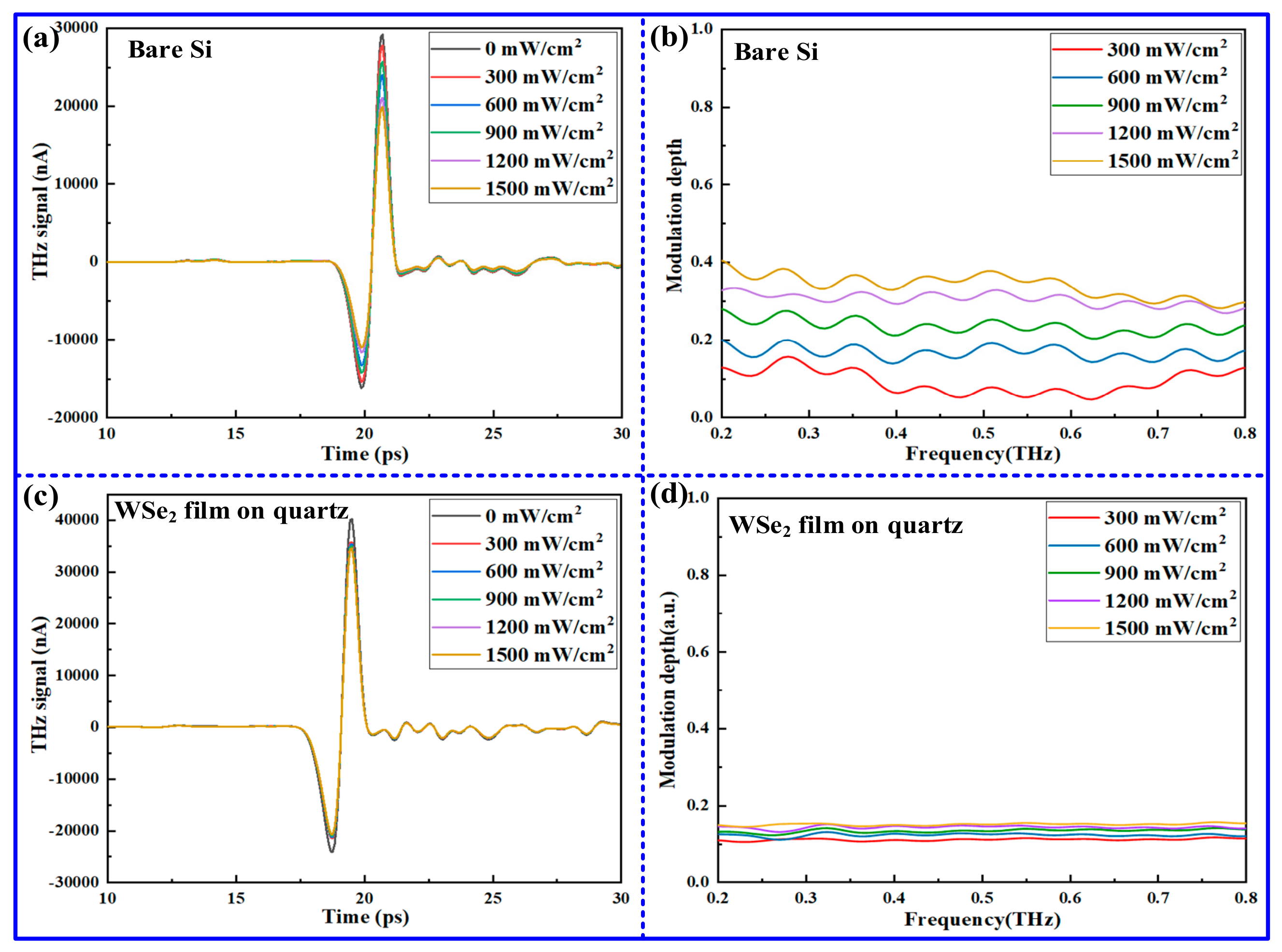
where and denote the THz amplitudes without and with pumping. Figure 4e shows the MD across 0.1–1.1 THz at different pump powers. The MD increases progressively with the increase in pump power from 300 to 1200 mW/cm2 and saturates above 1200 mW/cm2. At 1500 mW/cm2, a maximum MD of 72% is achieved at 0.5 THz. For comparison, Figure 5 shows the time-domain THz transmissions and MDs for bare Si and a WSe2 film on quartz under identical pumping. The WSe2/quartz sample exhibits much stronger time-domain signals; yet, its maximum MD is only 15%, compared with 40% for bare Si and 72% for WSe2/Si heterojunction. Thus, the heterojunction modulator achieves an MD approximately two times that of bare Si and five times that of the WSe2/quartz, highlighting the critical role of the heterojunction in boosting MD. Additionally, it is worth noting that the MD values in Figure 4e and Figure 5 are compared using incident pump power densities, a common practice in the literature [41,43]. However, the absorbed pump power may differ among samples owing to their distinct absorption at 850 nm. In the WSe2/Si heterojunction, the 500 nm WSe2 layer absorbs only a small fraction of the incident 850 nm light, because the pump penetration depth in Si (≈13 μm) is much larger than the WSe2 thickness. Consequently, the pump absorption is dominated by the Si substrate and is essentially the same as that of bare Si. Therefore, the direct comparison between WSe2/Si and bare Si remains valid. For the WSe2/quartz, the WSe2 film is the sole absorber, and its absorption at 850 nm is substantially lower than that of Si, so its effective absorbed pump power is much smaller, partially accounting for its low MD. Nevertheless, even after considering for the absorbed power, the WSe2/Si heterojunction still exhibits a markedly higher MD than bare Si, because the heterojunction enhances carrier lifetime and conductivity change, as discussed below. Hence, our main conclusion, that the heterojunction significantly boosts modulation performance, remains robust.
Figure 5.
THz signals and modulation depths of bare Si and WSe2/quartz. (a) bare Si (time-domain), (b) bare Si (MD), (c) WSe2/quartz (time-domain), (d) WSe2/quartz (MD).
Figure 4f shows the peak-to-peak time-domain signal as a function of pump power, displaying an approximately linear decrease with the increase in pump power from 0 to 1500 mW/cm2, indicating significant THz attenuation. Figure 4g plots the normalized transmission intensity versus pump power at 0.5 and 1.0 THz. Without pumping, transmission exceeds 0.88 at both frequencies, and at 1500 mW/cm2, it decreases to 0.28 (0.5 THz) and 0.17 (1.0 THz). The nearly identical trend confirms broadband operation. Figure 4h shows the MD dependence on pump power at same frequencies. With the increase in pump power, the MD increases rapidly and then saturates, reaching maximum values of 0.72 (0.5 THz) and 0.62 (1.0 THz) at 1500 mW/cm2. Compared with previously reported structures, moreover, our device exhibits a wide broadband and high MD, as shown in Table 3.
Table 3.
Comparison of modulation performance of previously reported THz modulators.
To elucidate the mechanism, we extracted the photo-induced complex conductivity from the measured complex transmission using Tinkham’s equation [45,46]:
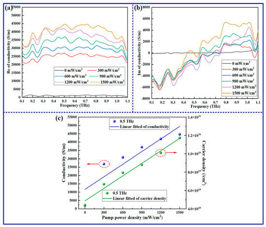
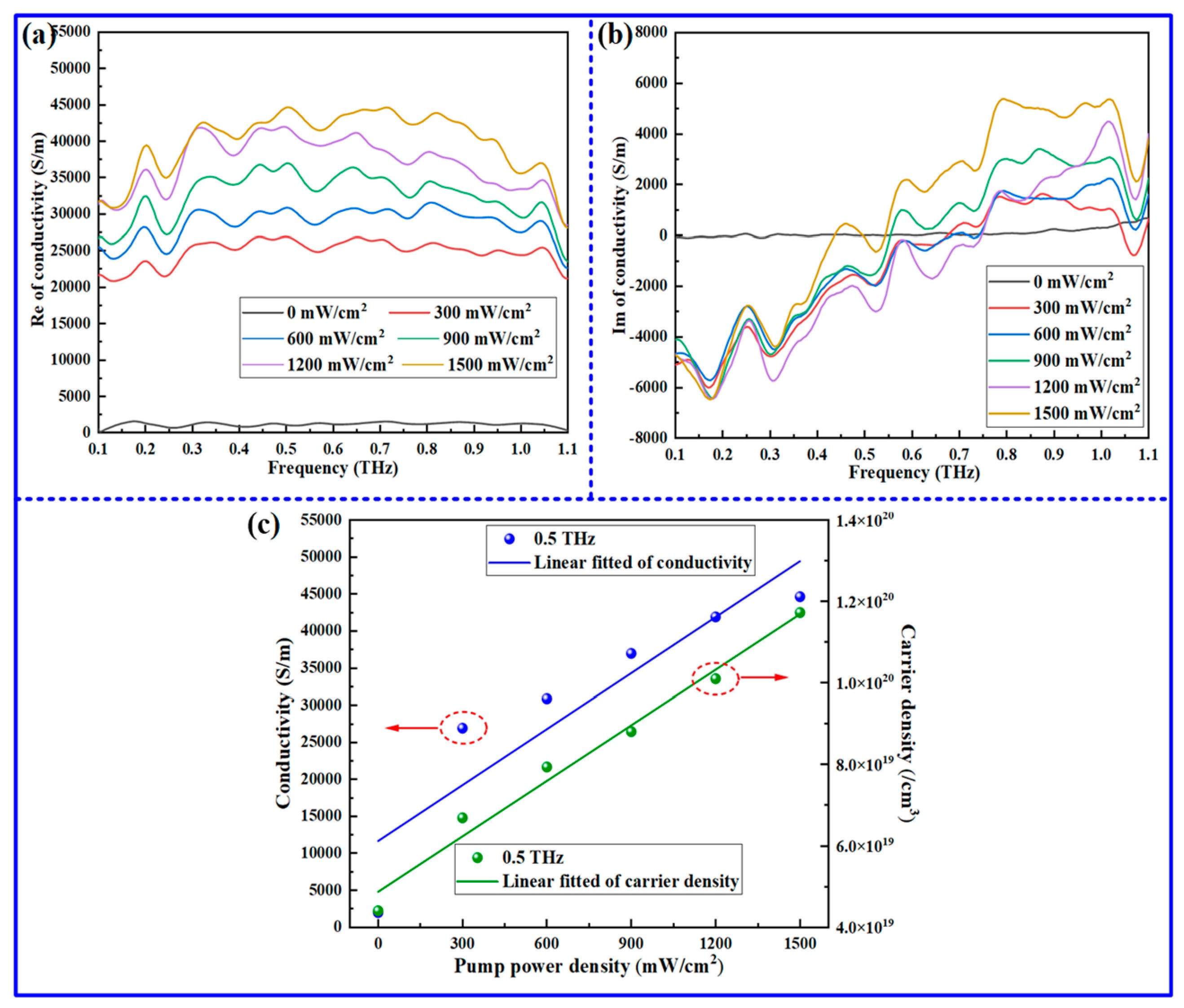
where is the free-space impedance, d is the effective photoconductive layer thickness, and is the refractive index of Si. Hence, the MD is mainly determined by the conductivity, which varies with the carriers’ dynamics. Under 850 nm CW pumping, it is important to quantitatively assess the pumping absorption from the 500 nm WSe2 film or/and the Si substrate. As discussed above, since quartz is insulating and generates no photocarrier, the WSe2/quartz sample achieves only 15% MD due to only 500 nm thickness, while bare Si reaches 40%. The low MD can be attributed that the 500 nm WSe2 film is too thin to produce enough photocarriers by itself. Hence, the conductivity change in the heterojunction arises from photogenerated charge carriers in both silicon and WSe2. However, the WSe2 film is much thinner than Si and absorbs only a minor fraction of the pumping light. The Si absorbs most of the laser power, with the majority of carriers generated in the penetration depth (≈13 μm). Thus, d is interpreted as the characteristic spatial extent of the photogenerated carrier population, i.e., the pump penetration depth in Si [47], and the thin-film condition (d ≪ λ) holds across 0.1–1.1 THz [48]. Figure 6 presents the real and imaginary parts of the complex conductivity as functions of frequency at different pump powers. The real part (Figure 6a) increases significantly with pump power, reducing the transmission and enhancing MD. In contrast, the imaginary part (Figure 6b), associated with phase modulation [49], exhibits only weak pump-power dependence, consistent with the negligible time shift observed in the inset of Figure 4b. These results indicate that the modulator is primarily suited for amplitude modulation.
Figure 6.
(a) Real part and (b) imaginary part of the complex conductivity of the WSe2/Si heterojunction, and (c) conductivity and carrier density as functions of pump power density.
To further quantify the carrier contribution, the complex conductivity was fitted using the Drude model [50]:
where ε0, Γ, ωp and are the vacuum permittivity, scattering rate, plasma frequency, and the backscattering coefficient, respectively. The plasma frequency relates to the charge carrier density via , where is the electron charge and is the effective mass. Figure 6c plots the conductivity and carrier density at 0.5 THz as functions of pump powers. Without pumping, the conductivity is near zero due to thermal equilibrium carriers. Upon excitation, both quantities increase linearly with pump power, reaching maximum values at 1500 mW/cm2, further confirming efficient modulation via pump intensity. Notably, the near-linear increase in extracted conductivity and carrier density does not contradict the apparent saturation of THz transmission and modulation depth at high pump powers (Figure 4e,f). This seeming discrepancy is reconciled by the nonlinear THz transmission–photoconductivity relationship inherent in the Tinkham’s equation [51]: the normalized transmission is given by . In the low-excitation regime ( ≪ 1), T decreases approximately linearly with increasing . At higher pump powers, however, becomes comparable to or greater than unity. Consequently, further increases in σ yield progressively smaller reductions in T, resulting in the observed saturation. Additionally, at high injection levels, Auger [52] and Shockley–Read–Hall [53] recombination become increasingly dominant, leading to a pump-dependent effective lifetime and a transition of the carrier density from linear to sublinear dependence on pump power [54]. Thus, the combined effect of the intrinsic Tinkham nonlinearity and high-injection recombination fully accounts for the saturation of the macroscopic THz response, while the linear fitting in Figure 6c remains physically valid across the moderate pump-power range (0–1500 mW/cm2), where linear recombination prevails.
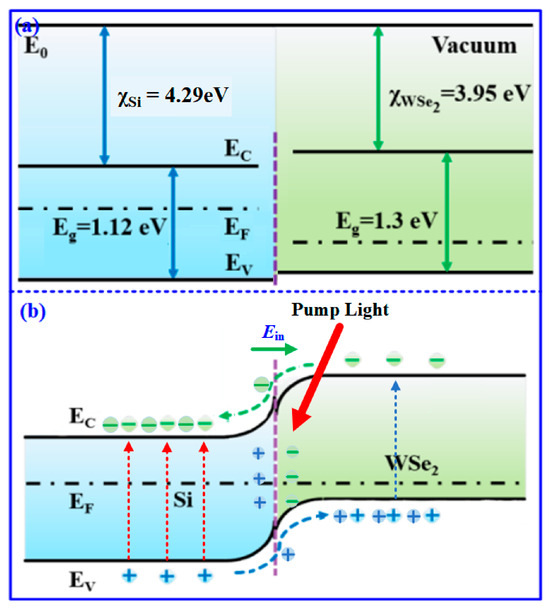
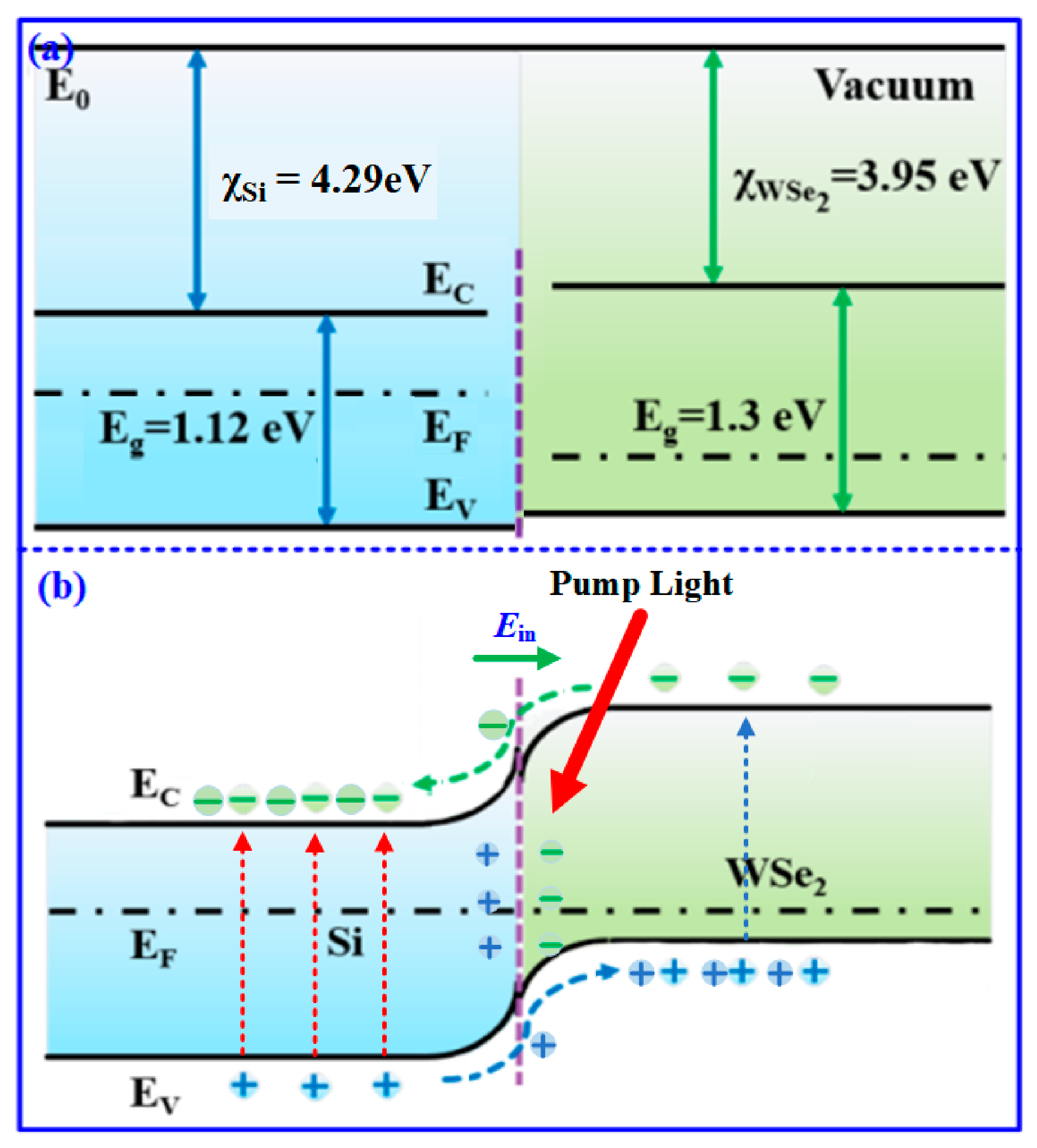
To further elucidate the enhanced conductivity and carrier density, the band alignment of the WSe2/Si heterojunction is shown in Figure 7a. Owing to the different bandgaps and Fermi levels in Si and WSe2, the conduction-band minimum (CBM) and valence-band maximum (VBM) are unaligned, creating an interfacial electric field. The electron affinity and bandgap differences yield a conduction-band offset of 0.05 eV and a valence-band offset of 0.13 eV, forming a type-II band alignment [55]. In high-resistivity Si (resistivity > 5000 Ω·cm and carrier concentration < 1013 cm−3), the Fermi level EF lies near midgap, while in WSe2, it lies close to the valence band, and is thus lower than that in Si. Upon contact, electrons diffuse from Si to WSe2 and holes in the opposite direction, establishing a built-in electric field (Ein) oriented from Si to WSe2 at equilibrium, as illustrated in Figure 7b.
Figure 7.
Band schemes of the WSe2/Si system: (a) energy bands of WSe2 and Si before contact and (b) band bending after contact and photogenerated carrier flow.
Under CW illumination, photocarriers are generated in both materials via interband transitions. However, because Si absorbs most of the pump power, it generates abundant photogenerated carriers, while WSe2 contributes only a few in WSe2. Moreover, the mobilities of the photogenerated electrons and holes in WSe2 are significantly lower than those in Si [56]. Therefore, the conductivity change in the heterojunction is dominated by the photocarriers in Si:
where μn and μp are the electron and hole mobilities in high-resistivity Si (1450 and 500 cm2/V·s, respectively), and Δn and Δp are the non-equilibrium carrier concentrations. Additionally, the recombination probability and lifetime τ of non-equilibrium electrons depend mainly on Δp, with τ ∝1/Δp [57]. Under the built-in electric field, photogenerated electrons transfer from WSe to Si while holes move in the opposite direction, enabling efficient separation of electrons and holes, as shown in Figure 7b. The separation reduces Δp in Si and suppresses electron-hole recombination, thereby prolonging the effective electron lifetime τ, increasing Δn in Si, and enhancing the MD. Since μn in high-resistivity Si is approximately three times μp, the Δσ is dominated by the enhanced electron population, leading to decreased THz transmission and increased MD [36]. Thus, the WSe2 layer acts not as a primary photoconductive channel but as an interfacial engineering layer that modulates carrier dynamics in Si and serves as a minority-carrier trap or surface-state mediator, similar to passivation layers in conventional semiconductor heterojunctions [28,29]. Thus, the enhanced modulation originates from interface-induced modifications to carrier dynamics in Si, not from direct photoconductive contributions of the WSe2 layer itself. In addition, the uneven surface morphology (Figure 2e,f) may enhance THz radiation trapping via an anti-reflection effect [58], further contributing to the large MD.
Additionally, the proposed band-alignment mechanism for enhancing the MD is further substantiated by recent experimental observations [59]. For example, time-resolved THz emission spectroscopy on monolayer WSe2/Si heterojunctions directly reveals an interface-induced drift-current amplification of up to one order of magnitude, demonstrating that the built-in electric field accelerates carriers migration and enhances photocurrent [36]. Concurrently, optical pump-terahertz probe (OPTP) measurements on pristine WSe2 show that photocarriers are generated on a sub-picosecond timescale and exhibit relaxation lifetimes of several hundred picoseconds, confirming that the intrinsic carrier dynamics in WSe2 enable ultrafast response while remaining long-lived enough to contribute meaningfully to the photoconductivity changes [60]. Collectively, these observations corroborate the proposed mechanism: the interfacial built-in electric field spatially separates electrons and holes, suppresses carrier recombination, prolongs the effective carrier lifetime, and thereby enhances net photoconductivity and THz MD.
Beyond modulation depth, modulation speed is a critical parameter for practical applications. Although our CW-pumping THz-TDS system is configured for steady-state transmission measurements and does not directly provide the frequency-dependent modulation response, the intrinsic carrier dynamics offer a reliable estimate for the response time. Using measured carrier lifetimes (τ ≈ 100–500 ps) reported in [60] and the interface-enhanced carrier separation described in [36], we estimate the intrinsic 3 dB modulation bandwidth of our WSe2/Si heterojunction modulator to be on the order of 1–2 GHz (BW ≈ 1/(2πτ)). A comprehensive experimental characterization of the modulation speed as a function of the chopping frequency will be pursued in future work, since the practical speed is also influenced by the chopper settings and external circuit parasitics.
4. Conclusions
In summary, we have successfully fabricated a large-area WSe2/Si heterojunction-based THz modulator with large MD using magnetron sputtering and vacuum selenization. The device exhibits a broadband response from 0.1 to 1.1 THz under 850 nm CW laser pumping. At a pump power density of 1500 mW/cm2, a maximum modulation depth of 72% is achieved at 0.5 THz, significantly surpassing those of bare Si and single WSe2 films. The enhanced performance is attributed to the heterojunction-induced built-in electric field, which effectively separates photogenerated carriers and suppresses recombination, thereby amplifying the conductivity change. Notably, compared with most reported THz modulators based on CVD-grown 2D materials, our heterojunction offers competitive modulation performance while being amenable to large-area fabrication. Therefore, this work provides a practical and scalable pathway for realizing effective THz modulation using large-area 2D film materials.
Author Contributions
Conceptualization, S.L., J.S. and G.L.; methodology, Y.L. and G.L.; validation, S.L. and D.H.; formal analysis, Y.L. and H.X.; investigation, S.L., J.S. and H.X.; data curation, H.X. and D.H.; writing—original draft preparation, S.L. and Y.L.; writing—review and editing, S.L. and G.L.; project administration, G.L. All authors have read and agreed to the published version of the manuscript.
Funding
The work is supported by the National Natural Science Foundation of China (62075052 and 6227419), National Key Research and Development Plan of China (2023YFB3210400), Science Foundation of the National Key Laboratory of Science and Technology on Advanced Composites in Special Environments (JCKYS2020603C009 and 6142905212711), and Project of Innovative and Entrepreneurship Training Program for College Students in Heilongjiang Province (201810214105).
Data Availability Statement
The original contributions presented in this study are included in the article. Further inquiries can be directed to the corresponding authors.
Conflicts of Interest
The authors declare no conflict of interest.
References
- Parrott, E.P.J.; Sun, Y.; Pickwell-MacPherson, E. Terahertz spectroscopy: Its future role in medical diagnoses. J. Mol. Struct. 2011, 1006, 66–76. [Google Scholar] [CrossRef] [Scilit]
- Siegel, P.H. Terahertz technology in biology and medicine. IEEE Trans. Microw. Theory Tech. 2004, 52, 2438–2447. [Google Scholar] [CrossRef] [Scilit]
- Koenig, S.; Lopez-Diaz, D.; Antes, J.; Boes, F.; Henneberger, R.; Leuther, A.; Tessmann, A.; Schmogrow, R.; Hillerkuss, D.; Palmer, R.; et al. Wireless sub-THz communication system with high data rate. Nat. Photonics 2013, 7, 977–981. [Google Scholar] [CrossRef] [Scilit]
- Wu, X.; Pan, X.; Quan, B.; Xu, X.; Gu, C.; Wang, L. Self-referenced sensing based on terahertz metamaterial for aqueous solutions. Appl. Phys. Lett. 2013, 102, 151109. [Google Scholar] [CrossRef] [Scilit]
- Chen, H.T.; Taylor, A.J.; Yu, N. A review of metasurfaces: Physics and applications. Rep. Prog. Phys. 2016, 79, 076401. [Google Scholar] [CrossRef] [Scilit] [PubMed]
- Rahm, M.; Li, J.S.; Padilla, W.J. THz wave modulators: A brief review on different modulation techniques. J. Infrared Millim. Terahertz Waves 2013, 34, 1–27. [Google Scholar] [CrossRef] [Scilit]
- Chatzakis, I.; Li, Z.; Benderskii, A.V.; Cronin, S.B. Broadband terahertz modulation in electrostatically-doped artificial trilayer graphene. Nanoscale 2017, 9, 1721–1726. [Google Scholar] [CrossRef] [Scilit] [PubMed]
- Chen, S.; Fan, F.; Miao, Y.; He, X.; Zhang, K.; Chang, S. Ultrasensitive terahertz modulation by silicon-grown MoS2 nanosheets. Nanoscale 2016, 8, 4713–4719. [Google Scholar] [CrossRef] [Scilit] [PubMed]
- Jessop, D.S.; Kindness, S.J.; Yao, L.; Braeuninger-Weimer, P.; Lin, H.; Ren, Y.; Ren, C.X.; Hofmann, S.; Zeitler, J.A.; Beere, H.E.; et al. Graphene based plasmonic terahertz amplitude modulator operating above 100 MHz. Appl. Phys. Lett. 2016, 108, 171101. [Google Scholar] [CrossRef] [Scilit]
- Degl’Innocenti, R.; Jessop, D.S.; Shah, Y.D.; Sibik, J.; Zeitler, J.A.; Kidambi, P.R.; Hofmann, S.; Beere, H.E.; Ritchie, D.A. Low-bias terahertz amplitude modulator based on split-ring resonators and graphene. ACS Nano 2014, 8, 2548–2554. [Google Scholar] [CrossRef] [Scilit] [PubMed]
- Chen, H.T.; Padilla, W.J.; Cich, M.J.; Azad, A.K.; Averitt, R.D.; Taylor, A.J. A metamaterial solid-state terahertz phase modulator. Nat. Photonics 2009, 3, 148–151. [Google Scholar] [CrossRef] [Scilit]
- Chan, W.L.; Chen, H.T.; Taylor, A.J.; Brener, I.; Cich, M.J.; Mittleman, D.M. A spatial light modulator for terahertz beams. Appl. Phys. Lett. 2009, 94, 213511. [Google Scholar] [CrossRef] [Scilit]
- Li, Q.; Tian, Z.; Zhang, X.; Singh, R.; Du, L.; Gu, J.; Han, J.; Zhang, W. Active graphene–silicon hybrid diode for terahertz waves. Nat. Commun. 2015, 6, 7082. [Google Scholar] [CrossRef] [Scilit] [PubMed]
- Zhang, B.; Lv, L.; He, T.; Chen, T.; Zang, M.; Zhong, L.; Wang, X.; Shen, J.; Hou, Y. Active terahertz device based on optically controlled organometal halide perovskite. Appl. Phys. Lett. 2015, 107, 093301. [Google Scholar] [CrossRef] [Scilit]
- Libon, I.H.; Baumgärtner, S.; Hempel, M.; Hecker, N.E.; Feldmann, J.; Koch, M.; Dawson, P. An optically controllable terahertz filter. Appl. Phys. Lett. 2000, 76, 2821–2823. [Google Scholar] [CrossRef] [Scilit]
- Kleine-Ostmann, T.; Pierz, K.; Hein, G.; Dawson, P.; Koch, M. Audio signal transmission over THz communication channel using semiconductor modulator. Electron. Lett. 2004, 40, 124–126. [Google Scholar] [CrossRef] [Scilit]
- Danila, O.; Gross, B.M. Towards highly efficient nitrogen dioxide gas sensors in humid and wet environments using triggerable-polymer metasurfaces. Polymers 2023, 15, 545. [Google Scholar] [CrossRef] [Scilit] [PubMed]
- Ono, M.; Hata, M.; Tsunekawa, M.; Nozaki, K.; Sumikura, H.; Chiba, H.; Notomi, M. Ultrafast and energy-efficient all-optical switching with graphene-loaded deep-subwavelength plasmonic waveguides. Nat. Photonics 2020, 14, 37–43. [Google Scholar]
- Chen, H.T.; Palit, S.; Tyler, T.; Bingham, C.M.; Zide, J.M.O.; O’hara, J.F.; Smith, D.R.; Gossard, A.C.; Averitt, R.D.; Padilla, W.J.; et al. Hybrid metamaterials enable fast electrical modulation of freely propagating terahertz waves. Appl. Phys. Lett. 2008, 93, 091117. [Google Scholar] [CrossRef] [Scilit]
- Chen, H.T.; Padilla, W.J.; Zide, J.M.O.; Bank, S.R.; Gossard, A.C.; Taylor, A.J.; Averitt, R. Ultrafast optical switching of terahertz metamaterials fabricated on ErAs/GaAs nanoisland superlattices. Opt. Lett. 2007, 32, 1620–1622. [Google Scholar] [CrossRef] [Scilit] [PubMed]
- Wang, L.; Jie, J.; Shao, Z.; Zhang, Q.; Zhang, X.; Wang, Y.; Sun, Z.; Lee, S. MoS2/Si heterojunction with vertically standing layered structure for ultrafast, high-detectivity, self-driven visible–near infrared photodetectors. Adv. Funct. Mater. 2015, 25, 2910–2919. [Google Scholar] [CrossRef] [Scilit]
- Weis, P.; Garcia-Pomar, J.L.; Hoh, M.; Reinhard, B.; Brodyanski, A.; Rahm, M. Spectrally wide-band terahertz wave modulator based on optically tuned graphene. ACS Nano 2012, 6, 9118–9124. [Google Scholar] [CrossRef] [Scilit] [PubMed]
- Wen, Q.Y.; Tian, W.; Mao, Q.; Chen, Z.; Liu, W.-W.; Yang, Q.-H.; Sanderson, M.; Zhang, H.-W. Graphene based all-optical spatial terahertz modulator. Sci. Rep. 2014, 4, 7409. [Google Scholar] [CrossRef] [Scilit] [PubMed]
- Cheiwchanchamnangij, T.; Lambrecht, W.R.L. Quasiparticle band structure calculation of monolayer, bilayer, and bulk MoS2. Phys. Rev. B—Condens. Matter Mater. Phys. 2012, 85, 205302. [Google Scholar] [CrossRef] [Scilit]
- Splendiani, A.; Sun, L.; Zhang, Y.; Li, T.; Kim, J.; Chim, C.-Y.; Galli, G.; Wang, F. Emerging photoluminescence in monolayer MoS2. Nano Lett. 2010, 10, 1271–1275. [Google Scholar] [CrossRef] [Scilit] [PubMed]
- Klimov, V.I. Optical nonlinearities and ultrafast carrier dynamics in semiconductor nanocrystals. J. Phys. Chem. B 2000, 104, 6112–6123. [Google Scholar] [CrossRef] [Scilit]
- Li, J.; Luo, L.; Huang, H.; Ma, C.; Ye, Z.; Zeng, J.; He, H. 2D behaviors of excitons in cesium lead halide perovskite nanoplatelets. J. Phys. Chem. Lett. 2017, 8, 1161–1168. [Google Scholar] [CrossRef] [Scilit] [PubMed]
- Cao, Y.; Gan, S.; Geng, Z.; Liu, J.; Yang, Y.; Bao, Q.; Chen, H. Optically tuned terahertz modulator based on annealed multilayer MoS2. Sci. Rep. 2016, 6, 22899. [Google Scholar] [CrossRef] [Scilit] [PubMed]
- Zheng, W.; Fan, F.; Chen, M.; Chen, S.; Chang, S.-J. Optically pumped terahertz wave modulation in MoS2-Si heterostructure metasurface. AIP Adv. 2016, 6, 075105. [Google Scholar] [CrossRef] [Scilit]
- Qiao, J.; Wang, S.; Wang, Z.; He, C.; Zhao, S.; Xiong, X.; Wang, S.; Zhang, X.; Tao, X. Ultrasensitive and Broadband All-Optically Controlled THz Modulator Based on MoTe2/Si van der Waals Heterostructure. Adv. Opt. Mater. 2020, 8, 2000160. [Google Scholar] [CrossRef] [Scilit]
- Jakhar, A.; Kumar, P.; Moudgil, A.; Dhyani, V.; Das, S. Optically pumped broadband terahertz modulator based on nanostructured PtSe2 thin films. Adv. Opt. Mater. 2020, 8, 1901714. [Google Scholar] [CrossRef] [Scilit]
- Lv, T.; Geng, Q.; He, X.; Zhang, M.; Maksimenko, S. Optically controlled high-performance terahertz modulator enabled by GeSe2/Si heterojunctions. Phys. E 2026, 177, 116448. [Google Scholar] [CrossRef] [Scilit]
- Pradhan, N.R.; Garcia, C.; Holleman, J.; Rhodes, D.; Parker, C.; Talapatra, S.; Terrones, M.; Balicas, L.; A McGill, S. Photoconductivity of few-layered p-WSe2 phototransistors via multi-terminal measurements. 2D Mater. 2016, 3, 041004. [Google Scholar] [CrossRef] [Scilit]
- Glemser, O.; Sauer, H.; König, P. Über Wolframsulfide und wolframselenide. Z. Anorg. Allg. Chem. 1948, 257, 241–246. [Google Scholar] [CrossRef] [Scilit]
- Zhang, X.; Shao, J.; Su, Y.; Wang, L.; Wang, Y.; Wang, X.; Wu, D. In-situ prepared WSe2/Si 2D-3D vertical heterojunction for high performance self-driven photodetector. Ceram. Int. 2022, 48, 29722–29729. [Google Scholar] [CrossRef] [Scilit]
- Song, F.; Zu, X.; Zhang, Z.; Jia, T.; Wang, C.; Huang, S.; Liu, Z.; Xuan, H.; Du, J. Ultrafast Drift Current Terahertz Emission Amplification in the Monolayer WSe2/Si Heterostructure. J. Phys. Chem. Lett. 2022, 13, 11398–11404. [Google Scholar] [CrossRef] [Scilit] [PubMed]
- Xia, C.; Fang, Z.; Huang, Y.; Wang, B.; Li, Z.; Wang, L.; Wu, X. All-optical Terahertz Modulation Based on WSe2-silicon Hybrid Structures. In Proceedings of the International Symposium on Ultrafast Phenomena and Terahertz Waves, Changsha, China, 23–26 April 2018; p. TuK39. [Google Scholar] [CrossRef] [Scilit]
- Li, H.; Gao, D.; Li, K.; Pang, M.; Xie, S.; Liu, R.; Zou, J. Texture control and growth mechanism of WSe2 film prepared by rapid selenization of W film. Appl. Surf. Sci. 2017, 394, 142–148. [Google Scholar] [CrossRef] [Scilit]
- Gao, K.; Bi, Q.; Wang, X.; Liu, W.; Xing, C.; Li, K.; Xu, D.; Su, Z.; Zhang, C.; Yu, J.; et al. Progress and future prospects of wide-bandgap metal-compound-based passivating contacts for silicon solar cells. Adv. Mater. 2022, 34, 2200344. [Google Scholar] [CrossRef] [Scilit] [PubMed]
- Jakhar, A.; Kumar, P.; Husain, S.; Dhyani, V.; Das, S. Integration of nanometer-thick 1T-TaS2 films with silicon for an optically driven wide-band terahertz modulator. ACS Appl. Nano Mater. 2020, 3, 10767–10777. [Google Scholar] [CrossRef] [Scilit]
- Yang, D.S.; Jiang, T.; Cheng, X.A. Optically controlled terahertz modulator by liquid-exfoliated multilayer WS2 nanosheets. Opt. Express 2017, 25, 16364–16377. [Google Scholar] [CrossRef] [Scilit] [PubMed]
- Hu, Y.; Tong, M.; Hu, S.; He, W.; Cheng, X.; Jiang, T. Reassessing Fano Resonance for Broadband, High-Efficiency, and Ultrafast Terahertz Wave Switching. Adv. Sci. 2023, 10, 2204494. [Google Scholar] [CrossRef] [Scilit] [PubMed]
- Xi, Y.; Zhou, Y.; Cao, X.; Wang, J.; Lei, Z.; Lu, C.; Wu, D.; Shi, M.; Huang, Y.; Xu, X. Broadband All-Optical THz Modulator Based on Bi2Te3/Si Heterostructure Driven by UV-Visible Light. Micromachines 2023, 14, 1237. [Google Scholar] [CrossRef] [Scilit] [PubMed]
- Lee, K.; Li, J.; Cheng, L.; Wang, J.; Kumar, D.; Wang, Q.; Chen, M.; Wu, Y.; Eda, G.; Chia, E.E.M.; et al. Sub-picosecond carrier dynamics induced by efficient charge transfer in MoTe2/WTe2 van der Waals heterostructures. ACS Nano 2019, 13, 9587–9594. [Google Scholar] [CrossRef] [Scilit] [PubMed]
- Yang, M.; Li, T.; Yan, X.; Liang, L.; Yao, H.; Sun, Z.; Li, J.; Li, J.; Wei, D.; Wang, M.; et al. Dual-stimulus control for ultra-wideband and multidimensional modulation in terahertz metasurfaces comprising graphene and metal halide perovskites. ACS Appl. Mater. Interfaces 2021, 14, 2155–2165. [Google Scholar] [CrossRef] [Scilit] [PubMed]
- Zhu, L.; Lai, T.; Jiang, H.; Ma, Y.; Dong, J. Ultrafast carrier dynamics of transition metal dichalcogenides and related heterostructures investigated via optical pump-terahertz probe spectroscopy. Laser Optoelectron. Prog. 2025, 62, 0700003. [Google Scholar]
- Wang, Y.; Sun, M.; Li, Z.; Lan, Z.; Lu, B.; Cheng, Z.; Xiao, M.; Jing, C.; Jin, Z. The conversion of positive-negative photoconductivity driven by photoexcited carriers in topological semimetal Co2MnAl thin films revealed with terahertz spectroscopy. Acta Phys. Sin. 2026, 75, 130409. [Google Scholar] [CrossRef] [Scilit]
- Neu, J.; Regan, K.P.; Swierk, J.R.; Schmuttenmaer, C.A. Applicability of the thin-film approximation in terahertz photoconductivity measurements. Appl. Phys. Lett. 2018, 113, 233901. [Google Scholar] [CrossRef] [Scilit]
- Buchnev, O.; Podoliak, N.; Kaltenecker, K.; Walther, M.; Fedotov, V.A. Metasurface-based optical liquid crystal cell as an ultrathin spatial phase modulator for THz applications. ACS Photonics 2020, 7, 3199–3206. [Google Scholar] [CrossRef] [Scilit]
- Srivastava, Y.K.; Chaturvedi, A.; Manjappa, M.; Kumar, A.; Dayal, G.; Kloc, C.; Singh, R. MoS2 for Ultrafast All-Optical Switching and Modulation of THz Fano Metaphotonic Devices. Adv. Opt. Mater. 2017, 5, 1700762. [Google Scholar] [CrossRef] [Scilit]
- Meged, M.S.; Zaitsev, A.D.; Demchenko, P.S.; Khodzitsky, M.K. Modified Tinkham’s Equation for Exact Computation of a Thin Film Terahertz Complex Conductivity. J. Infrared Millim. Terahertz Waves 2023, 44, 503–515. [Google Scholar] [CrossRef] [Scilit]
- Dziewior, J.; Schmid, W. Auger coefficients for highly doped and highly excited silicon. Appl. Phys. Lett. 1977, 31, 346–348. [Google Scholar] [CrossRef] [Scilit]
- Shockley, W.; Read, W.T. Statistics of the recombinations of holes and electrons. Phys. Rev. 1952, 87, 835–842. [Google Scholar] [CrossRef] [Scilit]
- Misiakos, K.; Park, J.S.; Neugroschel, A. Carrier lifetimes in highly injected silicon. J. Appl. Phys. 1990, 67, 2576–2582. [Google Scholar] [CrossRef] [Scilit]
- Rahul, L.; Arora, S.K.; Jha, S.N.; Kumaret, Y. Determination of band alignment in liquid exfoliated few-layer WSe2/SiO2 interface. Mater. Lett. 2022, 311, 131600. [Google Scholar] [CrossRef] [Scilit]
- Handa, T.; Holbrook, M.; Olsen, N.; Holtzman, L.N.; Huber, L.; Wang, H.I.; Bonn, M.; Barmak, K.; Hone, J.C.; Pasupathy, A.N.; et al. Spontaneous exciton dissociation in transition metaldichalcogenide monolayers. Sci. Adv. 2024, 10, eadj4060. [Google Scholar] [CrossRef] [Scilit] [PubMed]
- Chen, T.; Nam, Y.-H.; Wang, X.; Han, P.; Sun, W.; Feng, S.; Ye, J.; Song, J.-W.; Lee, J.-H.; Zhang, C. Effects of surface nanostructuring and impurity doping on ultrafast carrier dynamics of silicon photovoltaic cells: A pump-probe study. J. Phys. D Appl. Phys. 2018, 51, 024004. [Google Scholar] [CrossRef] [Scilit]
- Jakhar, A.; Dhyani, V.; Das, S. Room temperature terahertz detector based on single silicon nanowire junctionless transistor with high detectivity. Semicond. Sci. Technol. 2020, 35, 125014. [Google Scholar] [CrossRef] [Scilit]
- Johnson, N. Time Resolved Terahertz Spectroscopy of Photocarrier Dynamics in WSe2. Undergraduate Thesis, Department of Physics, Oregon State University, Corvallis, OR, USA, 2023. [Google Scholar]
- Han, P.; Wang, X.; Zhang, Y. Time-Resolved Terahertz Spectroscopy Studies on 2D Van der Waals Materials. Adv. Opt. Mater. 2020, 8, 1900533. [Google Scholar] [CrossRef] [Scilit]

Disclaimer/Publisher’s Note: The statements, opinions and data contained in all publications are solely those of the individual author(s) and contributor(s) and not of MDPI and/or the editor(s). MDPI and/or the editor(s) disclaim responsibility for any injury to people or property resulting from any ideas, methods, instructions or products referred to in the content. |
© 2026 by the authors. Licensee MDPI, Basel, Switzerland. This article is an open access article distributed under the terms and conditions of the Creative Commons Attribution (CC BY) license.