


Abstract
High-performance low dropout regulator (LDO) chips are core components that provide clean power for high-precision sensors, radio frequency (RF) circuits, low noise amplifiers and other noise-sensitive circuits. In the reported literature, the designed LDO chip has advantages in certain parameters, but it cannot meet all the requirements of a high power supply rejection ratio (PSRR), low output noise and low standby current at the same time, which makes the high-end applications of LDOs greatly limited. In this paper, an LDO chip with high PSRR, low output noise and low standby current has been designed and fabricated. By increasing the loop gain, introducing an improved feedforward path, and adopting isolated power supply, the PSRR of the LDO at different frequency bands is greatly improved. By optimizing the design of the error amplifier (EA) and adding a low-pass filter to filter out the reference noise, the output voltage noise of the LDO is reduced. Within the depletion process and an optimized reference structure, the standby power consumption of the LDO is reduced without damaging the output voltage accuracy. The chip is taped out with SMIC’s 0.18 μm/5 V/BCD process. The measured PSRR of the chip is as high as 95dB at a frequency of 1 kHz, and the high-frequency (1 MHz) PSRR is above 45 dB. The amplitude of integrated output noise is below 5.4 μVrms within the frequency range of 10 Hz to 100 KHz. When the load current is zero, the measured standby current is less than 400 nA. The test results indicate that the chip has excellent performance in terms of PSRR, output noise and standby power consumption.
1. Introduction
In the power management system, high-performance LDOs are widely used, especially in aerospace, 5G communication, weak analog signal detection and other applications that are very sensitive to power noise. An LDO with high PSRR can effectively filter the voltage ripple generated by the upper power stage, usually composed of switching convertors. The internal circuit of an LDO should not introduce additional noise into the output voltage, so the thermal noise and 1/f noise of the internal devices must be suppressed [1]. With the popularity of solar panels and lithium batteries as power supplies, to extend system runtime, ultra-low standby power consumption is required [2].
A common way to improve the PSRR is to use an N-type metal oxide semiconductor (NMOS) as the power MOSFET [3]. However, the drive voltage of NMOS needs to be raised by a charge pump, which makes the circuit design more complex and makes it difficult to achieve ultra-low power dissipation. In [4], a multi-stage voltage stabilization technology is adopted, and the PSRR of the LDO can reach 110 dB at 1 kHz, but this design does not take the power consumption into consideration. Mohamed El-Nozahi performed a detailed analysis of LDOs’ PSRR [5]. According to his work, the value of PSRR depends on the open-loop gain of the LDO. However, with the increase in operating frequency, the loop gain will gradually decline due to the parasitic capacitance, resulting in serious attenuation of PSRR at medium and high frequencies. Bangda Yang proposed a supply-noise cancellation technology by adding a feedforward path into the loop to effectively improve the high-frequency characteristics of PSRR [6]. However, the implementation of this method still consumes a lot of current and cannot achieve low standby current consumption. The integrated output noise of LDOs is mainly generated by the thermal noise and 1/f noise of internal devices. The most effective way to suppress device noise is to increase the bias current, which will also simultaneously increase the standby current.
In this paper, a two-stage operational amplifier is used to increase the open-loop gain to improve the DC-PSRR of the LDO chip. By inserting a coupling capacitor between a critical node of the operational amplifier and the power line, a feedforward path is formed, which introduces a pole-zero doublet, thus improving the high-frequency PSRR of the LDO. Since the reference voltage will fluctuate due to power supply ripple, and the fluctuation will be transmitted to the output through the error amplifier (EA), the PSRR of the reference voltage source needs to be improved. In [7], the power supply ripple is directly filtered out by a low-pass filter, which will seriously degrade the dynamic characteristics. In this paper, a low-pass filter is inserted between the reference voltage and the EA input, which can filter out the power fluctuation and the reference noise simultaneously. The output noise of the LDO mainly comes from the EA and the reference voltage source [8]. The power transistor contributes very little noise to the system due to its large area and its location at the system end. To reduce the noise of the EA, chopping technology is adopted [9]. However, this will greatly increase the power consumption of the chip. J. Mihhailov provided a detailed analysis of LDO noise at the system level [10]. The noise of the reference voltage is difficult to suppress by simply optimizing the circuit structure. In this paper, by optimizing EA design and inserting a low-pass filter between the reference and the EA’s negative input port, low output noise is achieved. In order to reduce the standby power consumption, a depletion process is adopted and the depletion N-type transistor is used in the design of the reference voltage source. The traditional depletion reference voltage source is realized by connecting the depletion and enhancement transistors in series [11,12], and the consumed current can be as low as 20 nA or less. The greatest disadvantage of the traditional structure is that the drift of the reference voltage is large and difficult to trim using fuses. To address this problem, the circuit is reconstructed and the reference voltage is generated by a current with zero temperature coefficient flowing through the resistor. In this paper, the characteristics of PSRR and output voltage noise are first analyzed, and then the key circuit is designed. Finally, the test results of the designed LDO chip are given.
2. Analysis of PSRR and Construction of Output Noise Model
2.1. Analysis of LDO’s PSRR
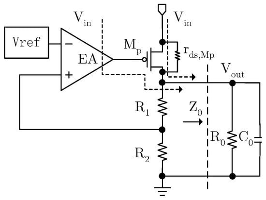
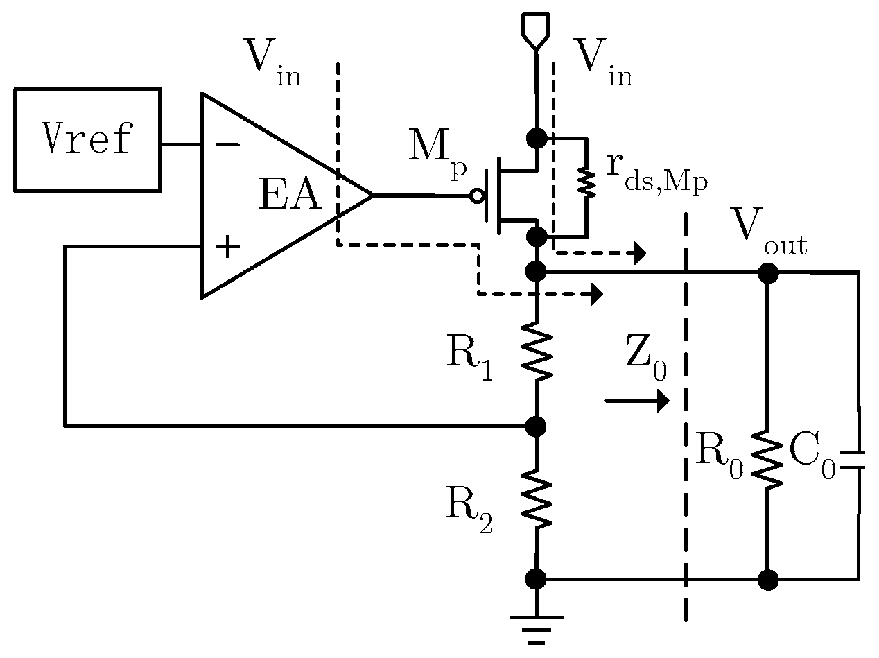
As shown in Figure 1, the power supply influences the output voltage of LDOs mainly through the power transistor, the EA and the reference voltage source. As the reference voltage is stabilized by the low-pass filter, the impact of the reference voltage on the PSRR of the system can be ignored. Firstly, the influence of the power supply Vin on the output voltage through the power transistor Mp is calculated. The output voltage variation will be fed back to the positive input port of the EA with the feedback ratio determined by the voltage divider resistors, and will be applied to the gate of Mp after being amplified by the EA. Based on the current balance at the output port, the following can be obtained:
Figure 1.
Path of PSRR.
ΔVout represents the variation in the output voltage, gMp is the transconductance of the power transistor, Aea represents the gain of the EA, rds,Mp represents the channel resistance of the power transistor and Z0 is the equivalent impedance at the output terminal. Due to their large values, R1 and R2 can be ignored in the calculation of Z0 to simplify the analysis. The relationship between the power supply variation and the output voltage can be expressed as
Equation (2) is the expression for the PSRR of the LDO that considers only the influence of the power transistor. It can be seen from Equation (2) that as the operation frequency is very low, the PSRR is determined entirely by the gain of the EA. However, as the frequency increases, the gain of the EA decreases due to parasitic capacitance, and the PSRR of the LDO will continue to deteriorate. Secondly, considering the path from the EA, by equating the impact of power supply variation on the EA output to that at the EA input port, the following expression can be derived:
ΔVin,ea represents the input voltage change of the EA caused by power supply variation, and PSRRea is the PSRR of the EA. Assuming that the output voltage change of the LDO is ΔVout, the closed-loop gain can be calculated:
Simplifying Equation (4), the following can be written:
Equation (5) indicates that when suppressing the influence of power supply variation on the LDO’s output voltage through the EA, the most effective way is to improve the PSRR of the EA. In summary, it can be concluded that to improve the PSRR of LDO, the DC gain of the EA should exceed the target value of the system’s PSRR, and its PSRR should be maximized.
2.2. Model of LDO Output Voltage Noise
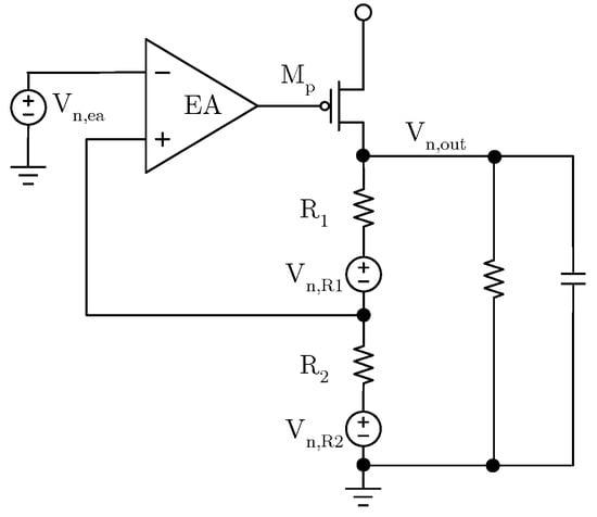
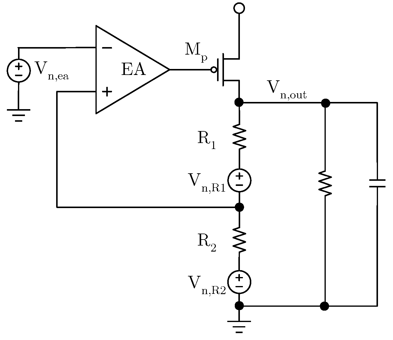
Due to the difficulty in suppressing the noise of the reference voltage, which can only be filtered out by a low-pass filter [13,14] and the negligible 1/f noise of the power transistor, the contribution of output voltage noise mainly comes from the EA and feedback resistors. As shown in Figure 2, Vn,ea is the equivalent input noise of the EA, Vn,R1 and Vn,R2 represent the thermal noise of R1 and R2, respectively, and Vn,out represents the noise at the output of the LDO. Since the noise has no direction, the sign of the noise is not considered. It can be concluded that
Figure 2.
Main noise source of LDO.
Equation (6) can be simplified:
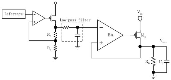
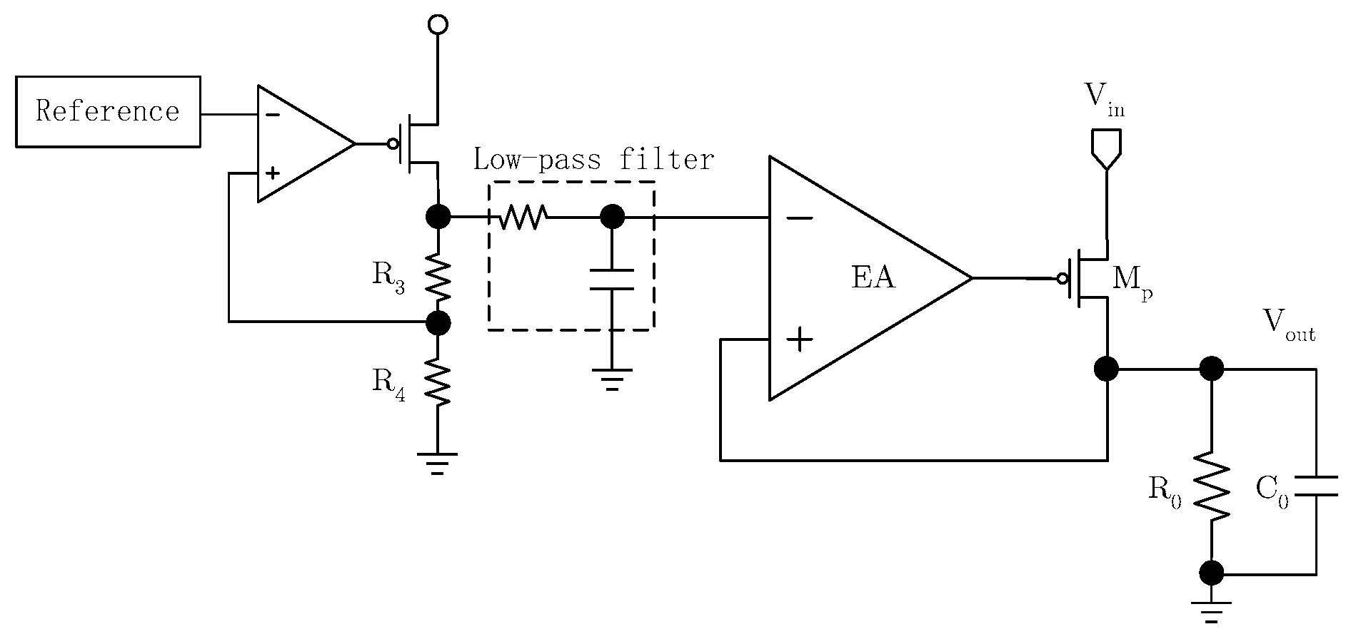
According to Equation (7), when R1 is zero, the output voltage noise is minimized. The equivalent input noise of the EA equals the LDO’s output voltage noise. In practice, it is impossible to completely eliminate the reference voltage noise. Consequently, the LDO’s output noise is mainly composed of the filtered reference voltage noise and the EA’s equivalent input noise. The overall LDO circuit schematic is shown in Figure 3. Since the output voltage is directly fed back to the EA’s positive input port, the reference voltage must first be pre-amplified and low-pass-filtered before it is applied to the EA’s negative input terminal. Since the 1/f noise of MOS transistors increases at a lower frequency, and the output noise within the frequency range of 10 Hz to 100 KHz is mainly concerned, the 3 dB bandwidth of the low-pass filter is designed to be around 1 Hz to 2 Hz. Moreover, during startup, the filter capacitor needs to be quickly pre-charged to avoid an excessively long startup time.
Figure 3.
Circuit scheme of LDO.
3. Design of the Key Circuit
3.1. Design of EA and Feedforward Path
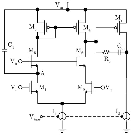
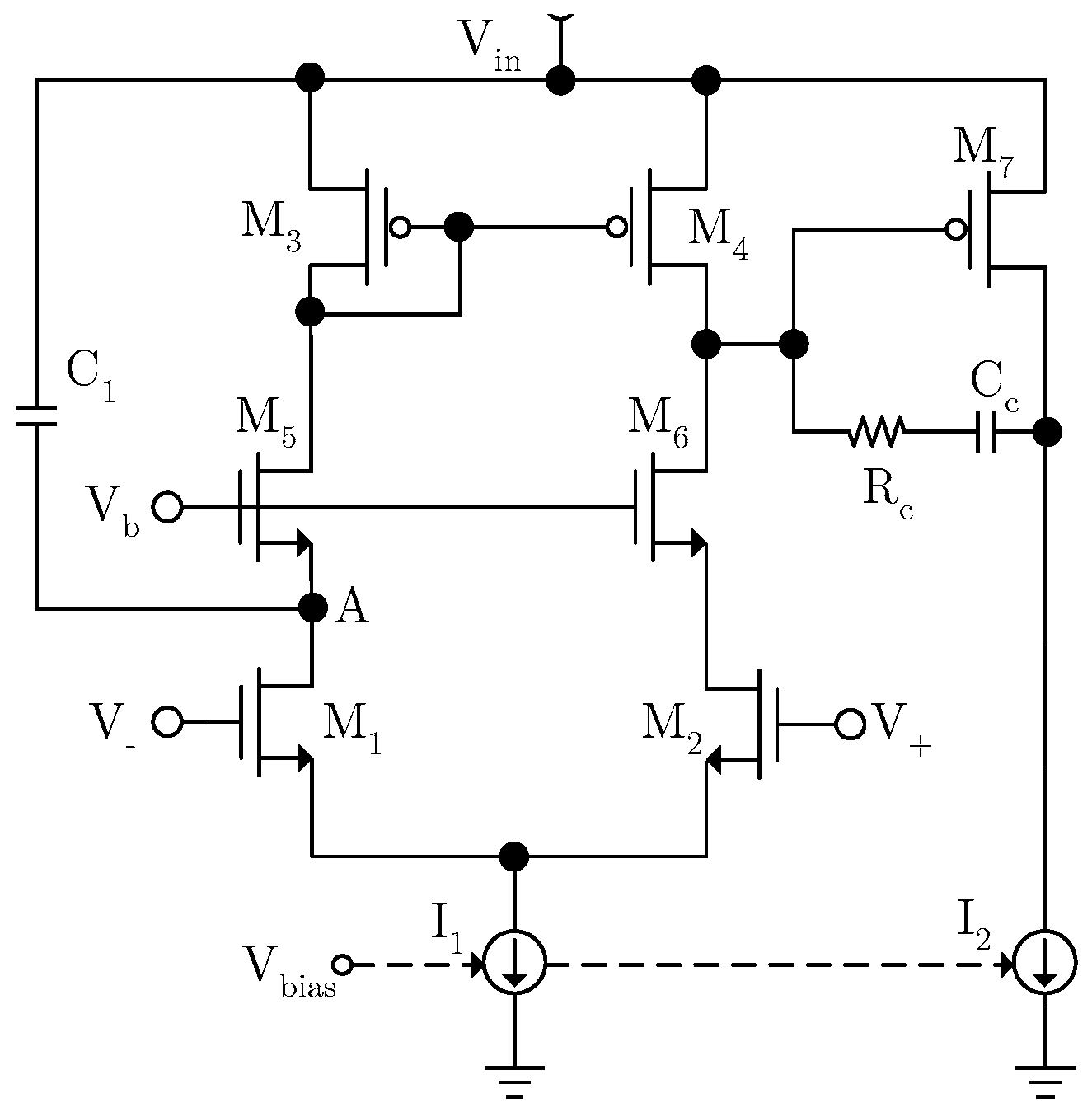
The design of the EA is especially crucial because its DC gain determines the upper limit of the PSRR of the LDO. A fast feedforward path is introduced by adding coupling capacitors between the power supply and the EA’s internal node [15,16]. The equivalent input noise of the EA is directly reflected at the output node. Furthermore, the system’s stability must be considered when designing the EA. The circuit is shown in Figure 4.
Figure 4.
Internal circuit of EA.
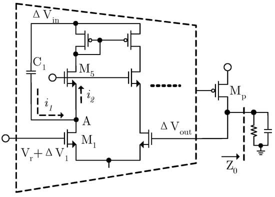
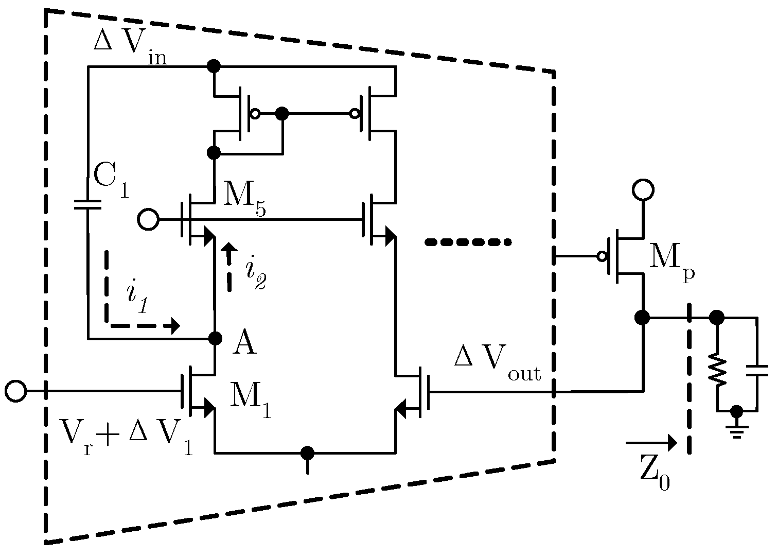
In order to improve DC gain, a two-stage operational amplifier is adopted, achieving a gain of 95 dB. M5 and M6 are used to suppress the influence of power supply ripple at the EA’s input and enhance the PSRR of the EA. P-type transistors are not used for power supply isolation, mainly because they will lead to excessive loop gain, making compensating the loop difficult. Additionally, due to the lower dominant pole, the transient response of the LDO cannot meet the requirements. The bias voltage Vb is a fixed voltage. Since the EA’s output directly drives the power transistor, its large parasitic capacitance creates a low-frequency pole at the EA’s output. To ensure system stability, Rc and Cc form Miller compensation, which pushes the EA’s output pole to a higher frequency. The dominant pole of the system is formed at the first stage of the EA. Since the zero introduced by Miller compensation cancels the LDO’s output pole, the maximum phase shift remains below 180 degrees, ensuring system stability. As the EA’s gain decreases with increasing frequency, the LDO’s high-frequency PSRR performance degrades. To address this, a coupling capacitor is inserted between the power supply and node A to improve the LDO’s high-frequency PSRR. The operating principle is illustrated in Figure 5.
Figure 5.
Operating principle of coupling capacitor.
Assuming that the variation in the power supply is ΔVin and the equivalent impedance seen from A is about 1/gm5, then the high-frequency coupling current is
gm5 is the transconductance of M5. The equivalent impedance seen from the source of M5 is quite small, and then the majority of the coupling current will flow into the current mirror from the source of M5 and influence the loop characteristics. For convenience of calculation, the coupling current is converted into the input voltage of the EA. This gives
gm1 is the transconductance of M1, and the coupling current is equivalent to the negative input of the EA. This gives
By substituting Equation (10) into Equation (9), this gives
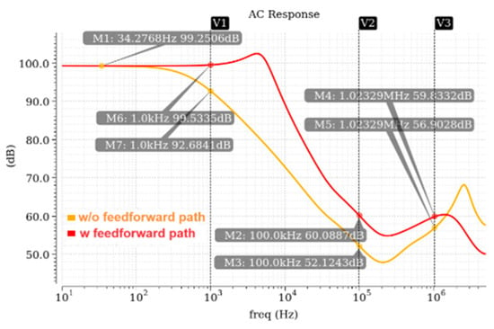
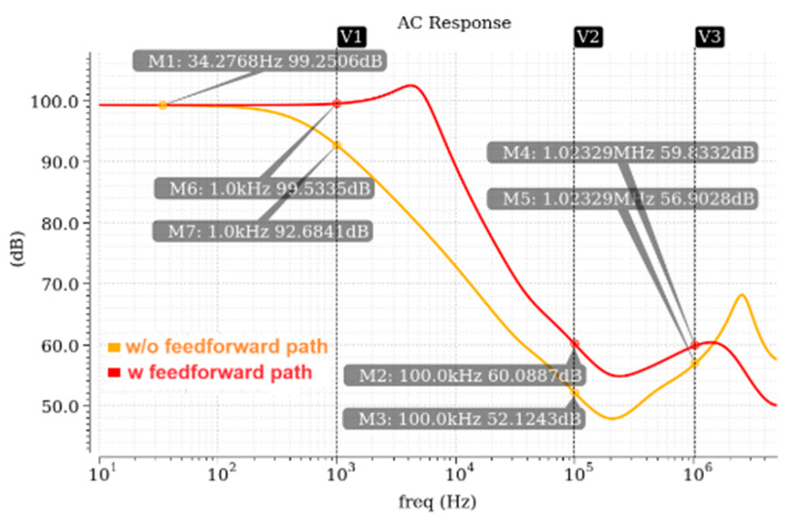
Equation (11) shows that the coupling capacitor introduces a pole-zero doublet into the PSRR transfer function, which will delay the decay rate of PSRR and improve the PSRR of the LDO in the middle–high-frequency band. Figure 6 shows the simulation comparison of PSRR with and without the improved feedforward path. The pole-zero doublet introduced by the feedforward path increases the dominant pole of the PSRR transfer function to around 5 kHz, improving the PSRR by approximately 7 dB at 1 kHz, 8 dB at 100 kHz, and 3 dB at 1 MHz. The overall PSRR performance is significantly improved.
Figure 6.
PSRR simulation wave with or without feedforward path.
3.2. Design of Depletion Reference Voltage Source
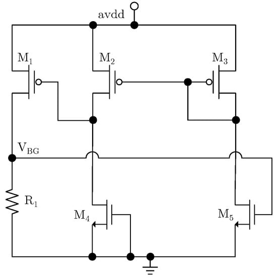
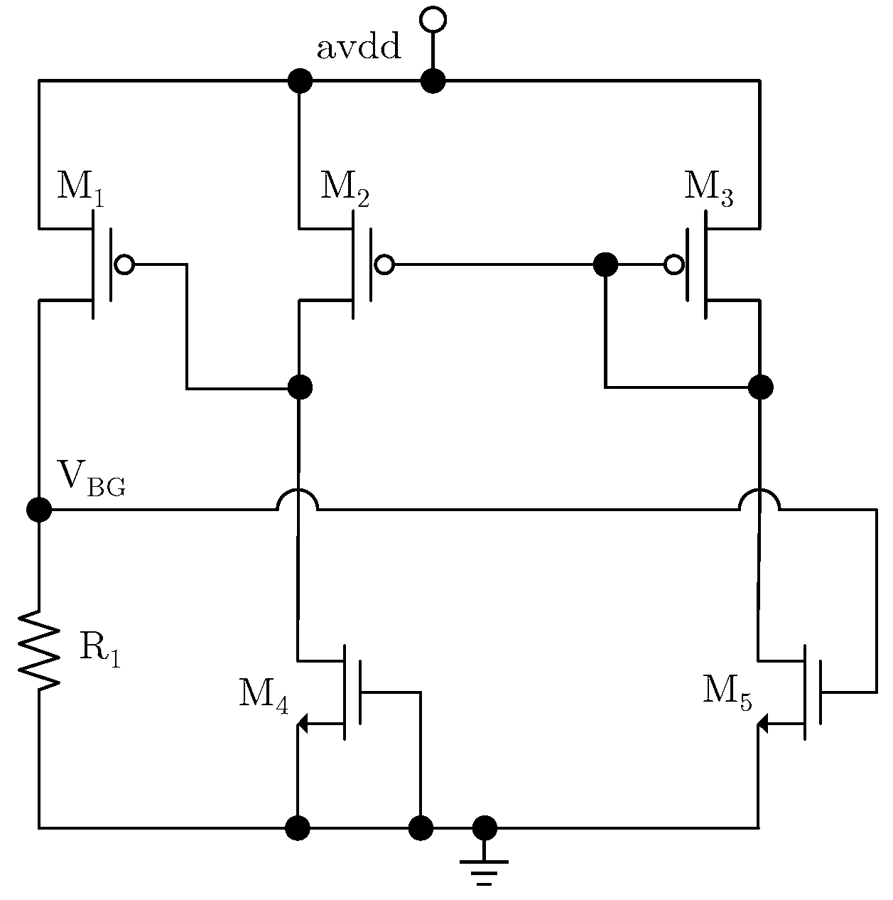
To reduce the standby power consumption of the chip, the reference voltage source is implemented with depletion technology. The voltage drift of the traditional depletion reference voltage source is usually large and difficult to trim back due to its series structure [17,18]. Azimi M. presents a subthreshold reference with an improved temperature coefficient through body bias curvature compensation [19]. However, this structure exhibits poor rejection of supply noise, resulting in low system PSRR. In this paper, a current mirror is adopted to mirror the current with a zero temperature coefficient onto a resistor to generate the reference voltage, which makes the reference voltage easy to trim and provides better rejection of power supply variations. The circuit is shown in Figure 7.
Figure 7.
Circuit of depletion reference voltage source.
As Figure 7 shows, M4 is a depletion transistor. The W/L ratios of M1, M2 and M3 are N:1:1, therefore, the current flowing through M4 and M5 is the same. Assuming a current I, this gives
Vth4 and Vth5 represent the threshold voltages of M4 and M5, respectively, while (W/L)4 and (W/L)5 are the aspect ratios of M4 and M5. Simplifying Equation (9) yields the following expression:
Since the threshold voltage of depletion-mode MOS transistors is negative, their temperature coefficient is opposite to that of enhancement-mode MOS transistors. Therefore, by adjusting the W/L ratios of M4 and M5, a reference voltage with zero temperature coefficient can be obtained. As shown in Figure 7, this gives
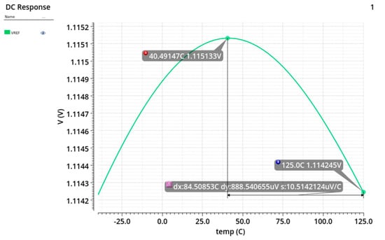
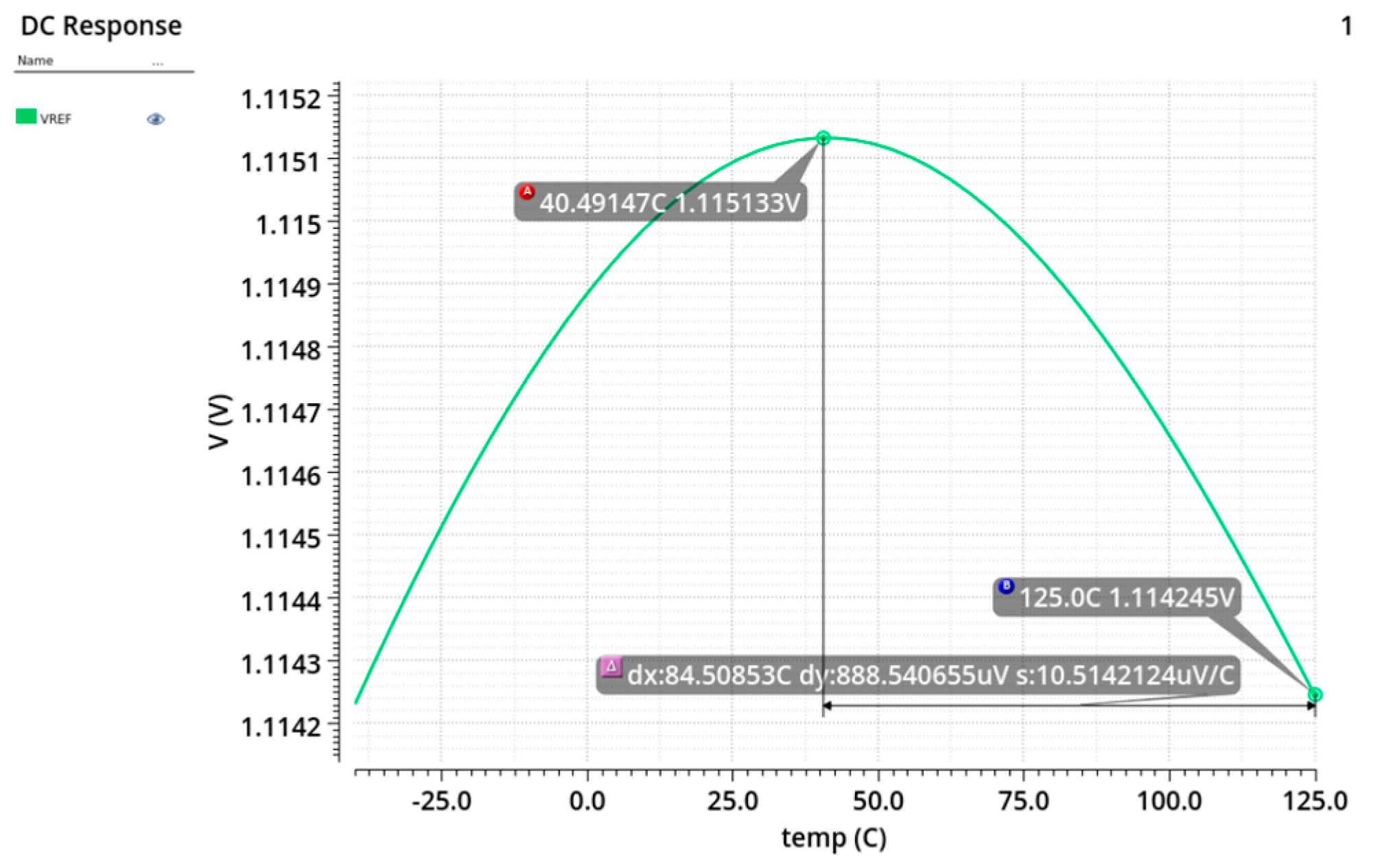
N is the current mirror ratio of M1. From Equation (14), the reference voltage can be adjusted by trimming the resistance of R1. Compared with the traditional depletion-mode reference voltage source, the circuit shown in Figure 7 significantly simplifies reference voltage trimming. To improve the PSRR, the depletion-mode reference voltage source is powered by a source-follower, which provides enhanced isolation from the power supply. Figure 8 shows the temperature DC sweep simulation result of the reference voltage. The average temperature coefficient (TC) of the simulated reference voltage is 9.48 ppm/°C.
Figure 8.
Temperature DC sweep simulation of the reference voltage: reference voltage vs. temperature.
4. Test Results
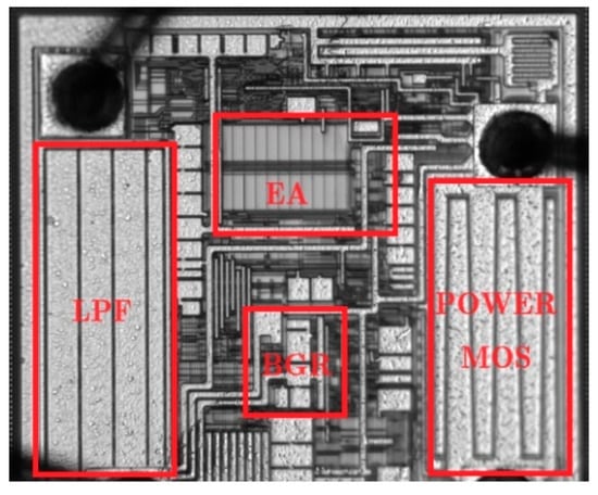
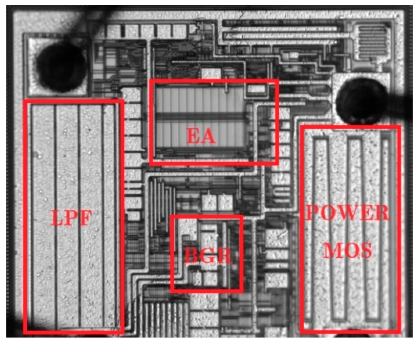
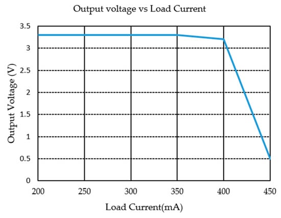
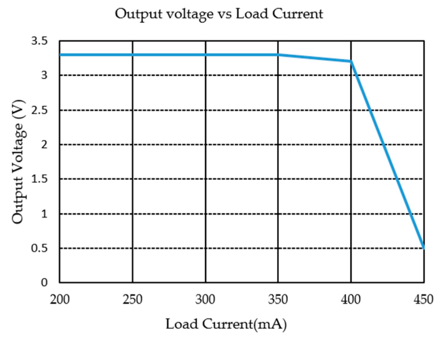
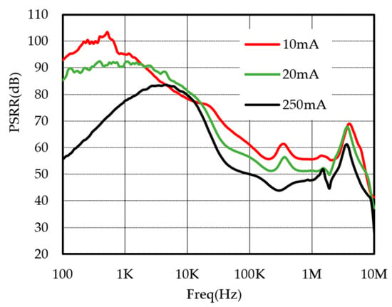
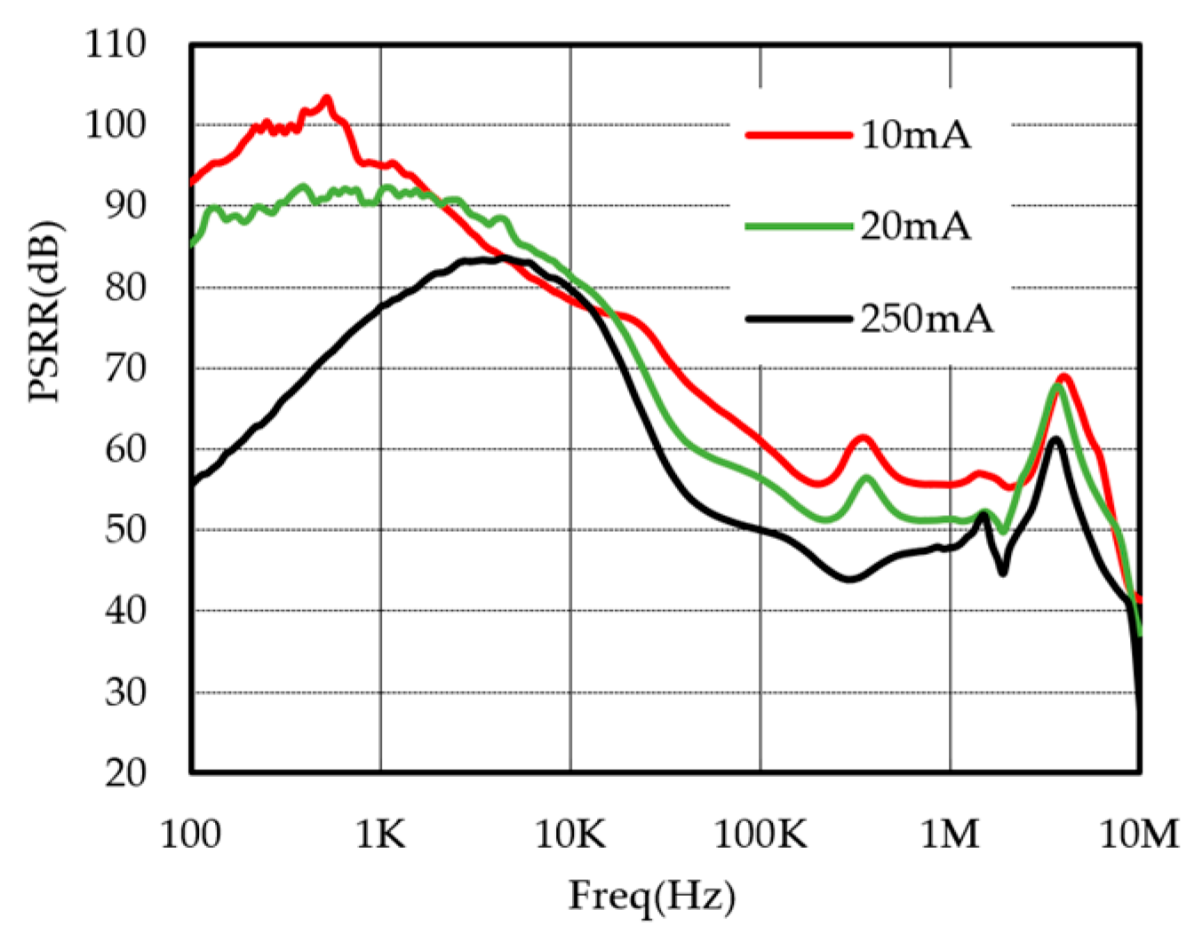
The LDO chip designed in this paper is fabricated with the SMIC 0.18-μm/5 V BCD process, and the total chip area is 0.27 mm2 (520 μm × 520 μm), as shown in Figure 9. The output voltage of the LDO is 3.3 V. The PSRR of the LDO was measured under varying load conditions with an input voltage of 4.3 V. Figure 10 shows the measurement results of the output voltage vs. load current. With an output voltage of 3.3 V and an output current limit of approximately 400 mA, the LDO can provide a sufficient current of 350 mA, meeting the requirements of the vast majority of applications. The PSRR test results are shown in Figure 11. When the load current is 10 mA, the PSRR at 1 kHz reaches 95 dB. By using of the feedforward path, the chip maintains a PSRR greater than 45 dB across the frequency from 100 kHz to 1 MHz. In contrast, the PSRR of other LDO products, such as the TPS7A21, drops below 20 dB within the same frequency band.
Figure 9.
Physical photo of LDO chip.
Figure 10.
The output voltage vs. load current.
Figure 11.
The measured PSRR of the chip.
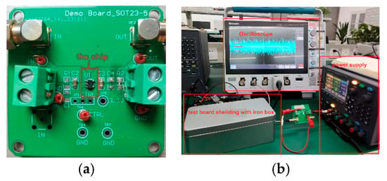
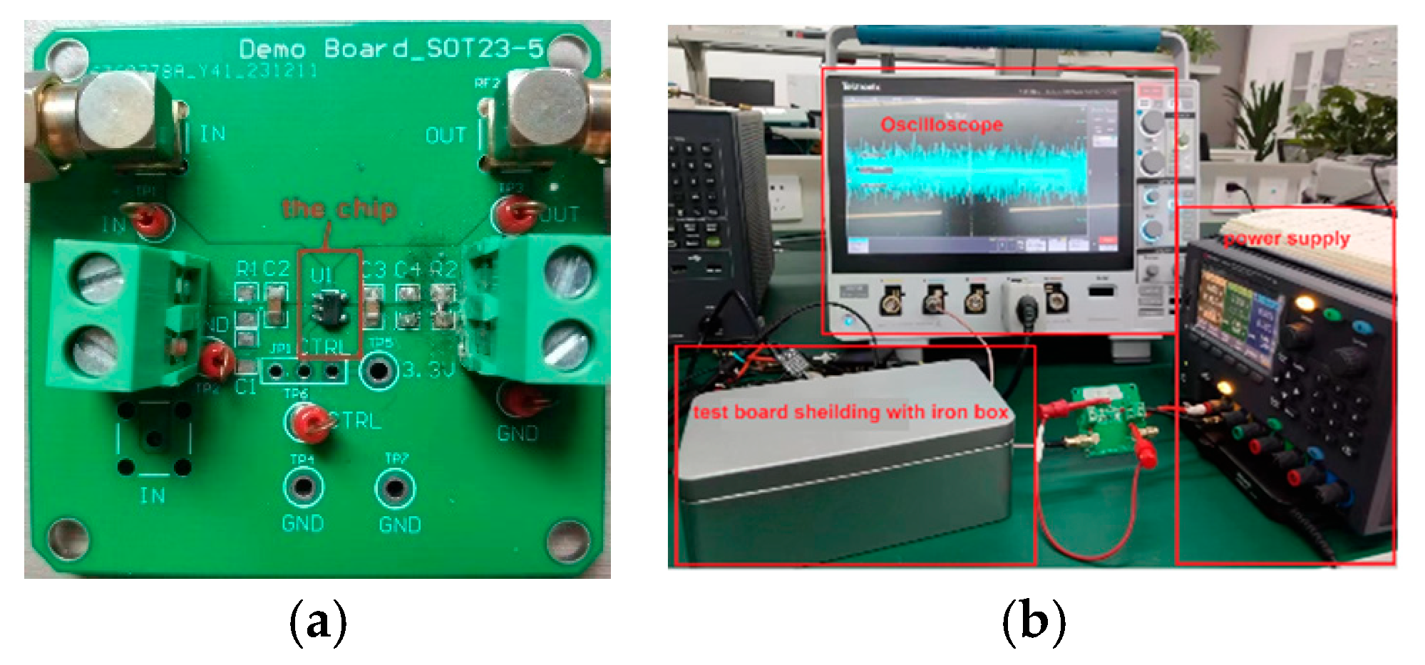
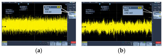
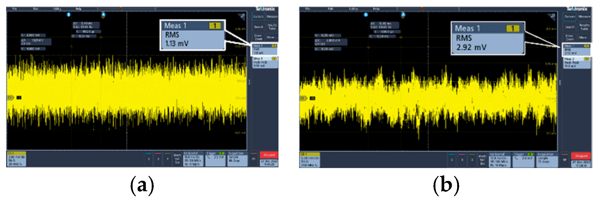
The amplitude of the output voltage noise is too small to be measured directly, so it needs to be amplified first, and the test board should be shielded with a metal box to avoid external noise interference [20]. The noise testing platform is shown in Figure 12, and the test results of LDO output voltage noise are shown in Figure 13. The overall amplified noise is 2.92 mVrms. Both the operational amplifier used for noise amplification and the oscilloscope contain a certain amount of noise, which needs to be removed. As shown in Figure 13, the measured noise of the oscilloscope and operational amplifier is 1.13 mVrms. Therefore, the calculated LDO output noise is 2.692 mVrms. When divided by an amplification factor of 500, the actual output voltage noise of the LDO is 5.384 μVrms.
Figure 12.
(a) Demo of the chip; (b) test bench of LDO output noise.
Figure 13.
(a) Wave of oscilloscope and operational amplifier noise; (b) overall LDO output noise.
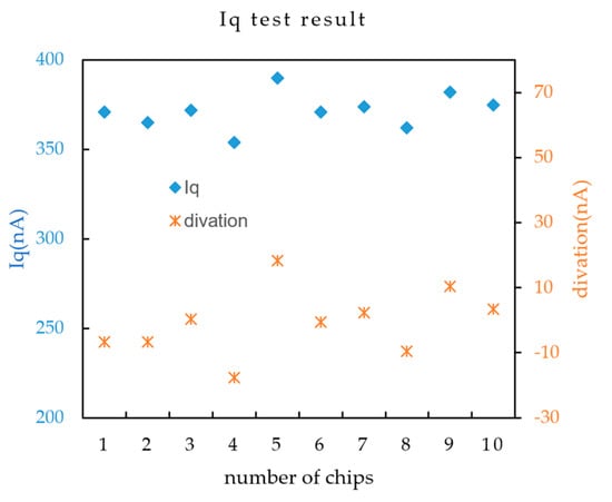
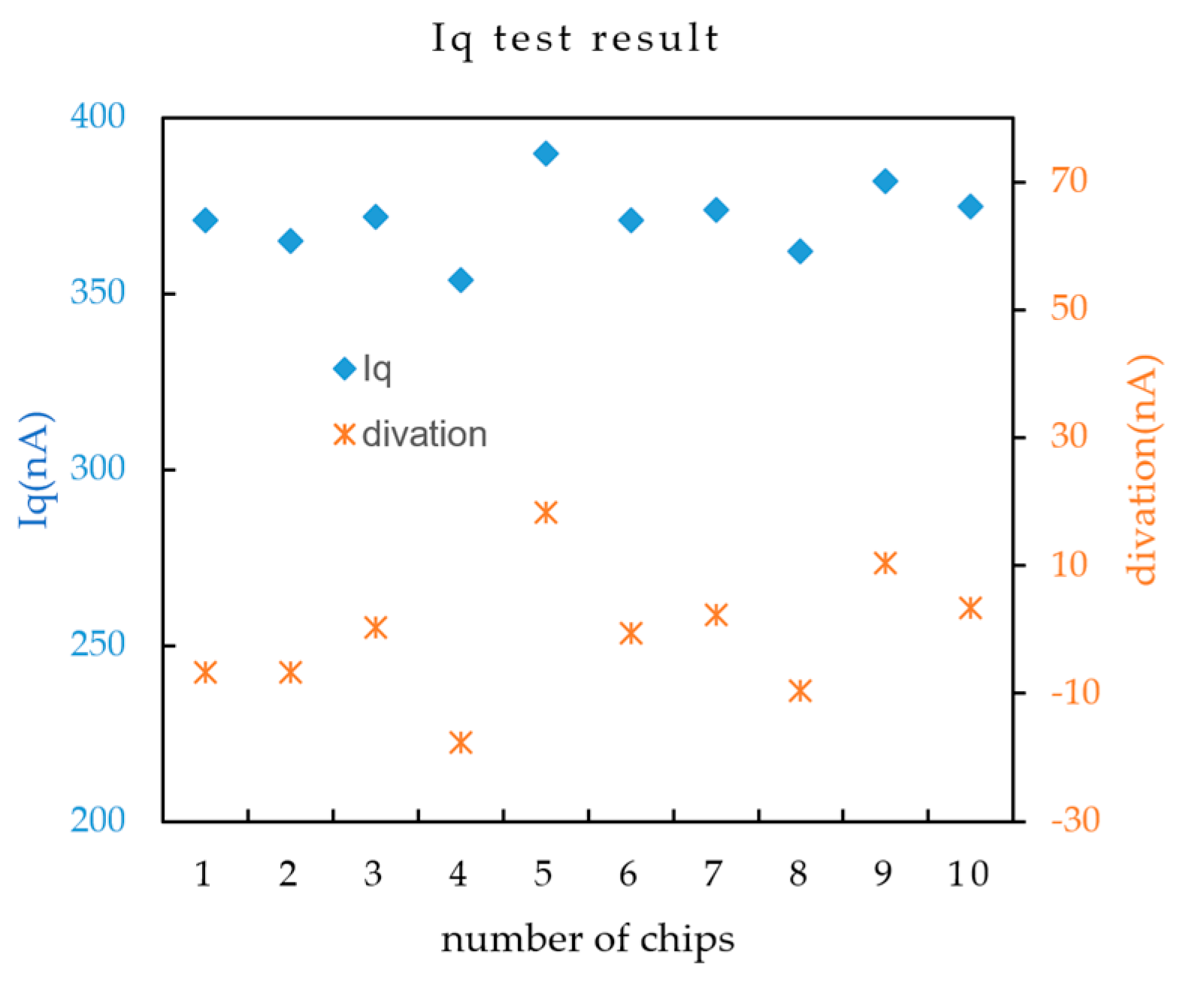
When the output load is zero, the current flowing from the ground pin is the standby current of the chip. A 100 Ω resistor connects the chip ground and the test board ground. The standby current is calculated by measuring the voltage drop across the resistor, which must be amplified with a low-offset, low-noise operational amplifier because the standby current is too small. The actual test results are shown in Figure 14, and the standby current of the chip is less than 400 nA, with a maximum deviation of less than 20 nA.
Figure 14.
Standby current test result.
Table 1 summarizes the performance comparison of the proposed LDOs. Compared with previous work, the LDO presented in this work exhibits significant advantages in standby power consumption while maintaining sufficient load capacity. Its PSRR and output noise performance are slightly lower than those of the LDO reported in reference [4], but the design in reference [4] generates a significantly higher quiescent current.
Table 1.
Performance summary of proposed LDO and comparison.
5. Conclusions
This paper presents a high-PSRR, low-noise, low-standby-current LDO chip. The measured PSRR of the chip reaches 95 dB. The output voltage noise is less than 6 μVrms, and the standby current is below 400 nA. The test results demonstrate that the chip has been successfully fabricated. A simplified feedforward path is designed and verified, which significantly improves the PSRR of the LDO in the mid-to-high frequency range. Additionally, a unique depletion-type reference voltage source is proposed, enabling easy trimming of the reference voltage and promoting the industrial application of high-performance LDO chips.
Author Contributions
Conceptualization, N.G., J.C., C.Y., C.C., C.L. and L.D.; methodology, N.G. and L.D.; software, N.G. and J.C.; validation, N.G. and C.C.; formal analysis, N.G. and C.L.; investigation, N.G.; resources, N.G. and L.D.; data curation, N.G.; writing—original draft preparation, N.G.; writing—review and editing, N.G., C.L. and L.D.; visualization, N.G., J.C. and C.Y.; project administration, N.G. and L.D.; funding acquisition, N.G. and L.D. All authors have read and agreed to the published version of the manuscript.
Funding
This research was supported in part by Luzhou Science and Technology Program (2024JYJ076), National Key Research and Development Program of China (No. 2023YFB3209600), Zhejiang Province Science and Technology Plan Project (No. 2025C01017), National Key R&D Plan (2022YFB3204800), the National Natural Science Foundation of China (No. U1909221 & No. 61871167), Zhejiang Provincial Talent Project (2021R52009).
Institutional Review Board Statement
Not applicable.
Informed Consent Statement
Not applicable.
Data Availability Statement
The original contributions presented in this study are included in the article. Further inquiries can be directed to the corresponding author.
Conflicts of Interest
The funders had no role in the design of the study; in the collection, analyses, or interpretation of the data; in the writing of the manuscript; or in the decision to publish the results.
Abbreviations
The following abbreviations are used in this manuscript:
| PSRR | Power supply rejection ratio |
| LDO | Low dropout regulator |
| RF | Radio frequency |
| EA | Error amplifier |
| NMOS | N-type metal oxide semiconductor |
References
- Luo, Y.; Wang, J.; Yuan, H.; Wei, T.; Huang, Y.; Wu, F.; Liu, Y.; Chu, X. Calculation of the worst-case voltage noise for a power distribution network based on ramp current. IEEE Trans. Circuits Syst. 2024, 71, 2797–2809. [Google Scholar]
- Kim, J.S.; Javed, K.; Min, K.H.; Roh, J. A 13.5-nA quiescent current LDO with adaptive ultra-low-power mode for low-power IoT applications. IEEE Trans. Circuits Syst. 2023, 70, 3278–3282. [Google Scholar] [CrossRef] [Scilit]
- Shao, L.; Xi, R.; Ding, Y.; Gong, B.; Lin, Y.; Zhao, L.; Qu, W. A low noise high PSR LDO based on N-type flipped voltage follower. In Proceedings of the 2022 IEEE International Power Electronics and Application Conference and Exposition (PEAC), Guangzhou, China, 4–7 November 2022; pp. 280–283. [Google Scholar]
- Wu, J.; Yao, S.; Liu, Z.; Chen, Z.; Wei, W.; Yu, H. A design of high PSRR low noise LDO circuit based on active filter circuit. Microelectron. Comput. 2024, 2, 67–75. [Google Scholar] [CrossRef]
- El-Nozahi, M.; Amer, A.; Torres, J.; Entesari, K.; Sanchez-Sinencio, E. High PSR low drop-out regulator with feed-forward ripple cancellation technique. IEEE J. Solid-State Circuits 2010, 45, 565–577. [Google Scholar] [CrossRef] [Scilit]
- Yang, B.; Drost, B.; Rao, S.; Hanumolu, P.K. A high-PSR LDO using a feedforward supply-noise cancellation technique. In Proceedings of the 2011 IEEE Custom Integrated Circuits Conference (CICC), San Jose, CA, USA, 19–21 September 2011; pp. 1–4. [Google Scholar]
- He, S. Research of Ultra-Low Noise, High PSRR LDO Regulator. Master’s Thesis, Xidian University, Xi’an, China, 2018. [Google Scholar]
- Mannama, V.; Sabolotny, R.; Strik, V. Ultra low noise low power LDO design. In Proceedings of the 2006 International Biennial Baltic Electronics Conference, Tallinn, Estonia, 2–4 October 2006; pp. 1–4. [Google Scholar]
- Oh, W.; Bakkaloglu, B.; Aravind, B.; Hoon, S.K. A low 1/f noise CMOS low-dropout regulator with current-mode feedback buffer amplifier. In Proceedings of the IEEE Custom Integrated Circuits Conference 2006, San Jose, CA, USA, 10–13 September 2006; pp. 213–216. [Google Scholar]
- Mihhailov, J.; Strik, V.; Strik, S.; Rang, T. Low noise LDO architecture with consideration for low voltage operation. In Proceedings of the 2014 14th Biennial Baltic Electronic Conference (BEC), Tallinn, Estonia, 6–8 October 2014; pp. 41–44. [Google Scholar]
- Hongnan, Z.; Zhiwei, Z. Design of novel voltage reference based on depletion device. In Proceedings of the 2009 9th International Conference on Electronic Measurement & Instruments, Beijing, China, 16–19 August 2009. [Google Scholar]
- Yan, M.; Jiao, L.; Liu, Y. Design of an ultra-low power voltage reference. Microelectronics 2020, 50, 171–175. [Google Scholar] [CrossRef]
- Magod, R.; Suda, N.; Ivanov, V.; Balasingam, R.; Bakkaloglu, B. A low-noise output capacitorless low-dropout regulator with a switched-RC bandgap reference. IEEE Trans. Power Electron. 2017, 32, 2856–2864. [Google Scholar] [CrossRef] [Scilit]
- Michailidis, A.; Noulis, T.; Siozios, K. CMOS noise analysis and simulation from low frequency and baseband to RF and millimeter wave. IEEE Access 2023, 11, 39807–39823. [Google Scholar] [CrossRef] [Scilit]
- Fan, H.; Feng, L.; Diao, X.; Xie, X.; Wang, C.; Li, G.; Wei, Q.; Qiao, F.; Feng, Q.; Bonizzoni, E. A fast transient LDO regulator featuring high PSRR over 100-kHz frequency range with adaptive, dynamic biasing, and current mode feed-forward amplifier. IEEE Trans. Circuits Syst. II Express Briefs 2024, 71, 1764–1768. [Google Scholar] [CrossRef] [Scilit]
- Tong, X.; Li, M.; Dong, S. A capacitor-less low dropout regulator with fast response. J. Electron. Inf. Technol. 2019, 41, 2592–2598. [Google Scholar]
- Chi, C. Research and Design of Ultra-Low Power Consumption BOOST Converter. Master’s Thesis, University of Electronic Science and Technology of China, Chengdu, China, 2023. [Google Scholar]
- Huang, G.; Yin, T.; Zhu, Y.; Xu, X.; Zhang, Y.; Yang, H. A -100dB Power Supply Rejection Ratio Non-bandgap Voltage Reference. J. Electron. Inf. Technol. 2016, 38, 2122–2128. [Google Scholar]
- Azimi, M.; Habibi, M.; Crovetti, P. A Two-Stage Sub-Threshold Voltage Reference Generator Using Body Bias Curvature Compensation for Improved Temperature Coefficient. Electronics 2024, 13, 1390. [Google Scholar] [CrossRef] [Scilit]
- Basar, E. Communication by means of thermal noise: Toward networks with extremely low power consumption. IEEE Trans. Commun. 2023, 71, 688–699. [Google Scholar] [CrossRef] [Scilit]

Disclaimer/Publisher’s Note: The statements, opinions and data contained in all publications are solely those of the individual author(s) and contributor(s) and not of MDPI and/or the editor(s). MDPI and/or the editor(s) disclaim responsibility for any injury to people or property resulting from any ideas, methods, instructions or products referred to in the content. |
© 2026 by the authors. Licensee MDPI, Basel, Switzerland. This article is an open access article distributed under the terms and conditions of the Creative Commons Attribution (CC BY) license.