


Abstract
This paper proposes a system-in-package combination navigation chip. We used wire bonding, chip stacking, surface mount, and other processes to integrate satellite navigation chips, inertial navigation chips, microprocessor chips, and separation devices. Finally, we realized the hardware requirements for combined navigation in a 20 mm × 20 mm chip. Further, we performed a multi-physics simulation analysis of the package design. For antenna signals, the insertion loss was greater than −1 dB@1 GHz and the return loss was less than −10 dB@1 GHz. The amplitude of these noises of the signal between the MCU and the IMU was approximately 20%, and the maximum value of the coupling coefficient between signal lines on the top surface was 13.4174%. The ninth mode of the power plane yielded a maximum voltage of 55 mV, and all power delivery networks had a DC voltage drop of less than 2%. The highest temperature in the microsystem was approximately 42 °C. These results show that our design performed well in terms of signal, power, and thermal performance.
1. Introduction
As the cost of advanced process nodes becomes more and more expensive, the economic benefits of Moore’s Law have become invalid. Compared with the design complexity and low yield caused by integrating all functions on a single big silicon chip, system-in-package (SiP) provides a more flexible, efficient, and low-cost development direction that integrates multiple components, such as a CPU, digital logic, analog/mixed signals, memory, sensors, and passive and discrete components, within a single package and a single system. SiP has attracted much research in recent years, which promotes its application in the fields of high-performance computing (HPC), multi-sensor fusion, radio frequency, power electronics, and other fields [1,2,3,4,5]. With the continuous development of integrated circuit technology, electronic products are increasingly developing in the directions of miniaturization, intelligence, high performance, and high reliability. In this process, SiP plays an important role and is widely used [6,7,8].
System-in-package often faces multi-physics and multi-scale problems, which are key issues in their design and simulation [9,10,11,12]. When finite element analysis is performed on components with large size differences, such as chips, packages, and circuit boards, a large number of meshes are generated, which cause difficulty and usually require simplified and reduced-order processing; this problem, however, was not the focus of this study. In order to ensure that microsystems can operate well and be highly reliable, researchers have chronically paid attention to and analyzed their electrical, thermal, mechanical and other properties, as well as the coupling characteristics existing in them [13,14,15,16]. To achieve system-level performance, signal integrity and power integrity are inescapable issues and challenges [17,18,19]. The signal path between chips needs to be high-speed and low-noise, while the power plane needs to provide stable voltage and sufficient current. In addition, microsystems need good heat dissipation to avoid performance degradation and failures caused by high temperatures [20,21,22,23]. Temperature causes thermal stress, and temperature mismatch is the main cause of the warping of microsystem structures [24]. Warpage and stress are the main causes of microsystem failure which affects reliability and yield, so it has become a research hotspot and attracted countless scholars [25,26,27,28,29,30]. However, most of the above studies discuss only the single-physics problem, and fail to obtain the results of multi-physics coupling, which are obviously deviated from the actual situation.
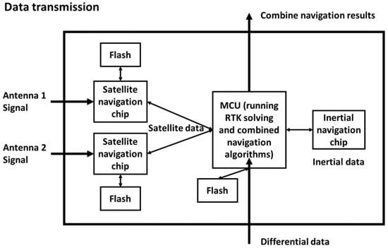
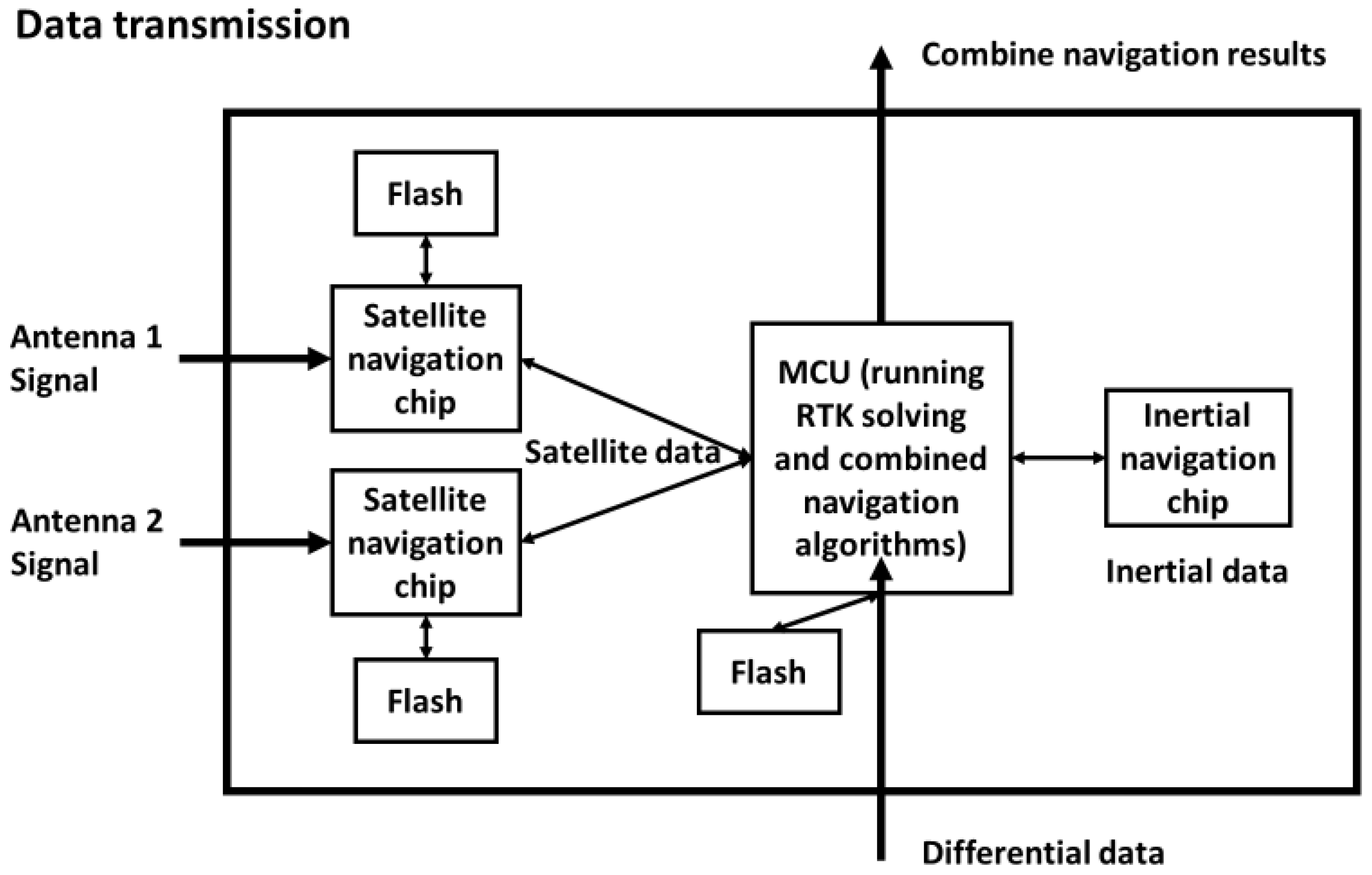
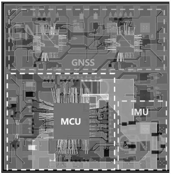
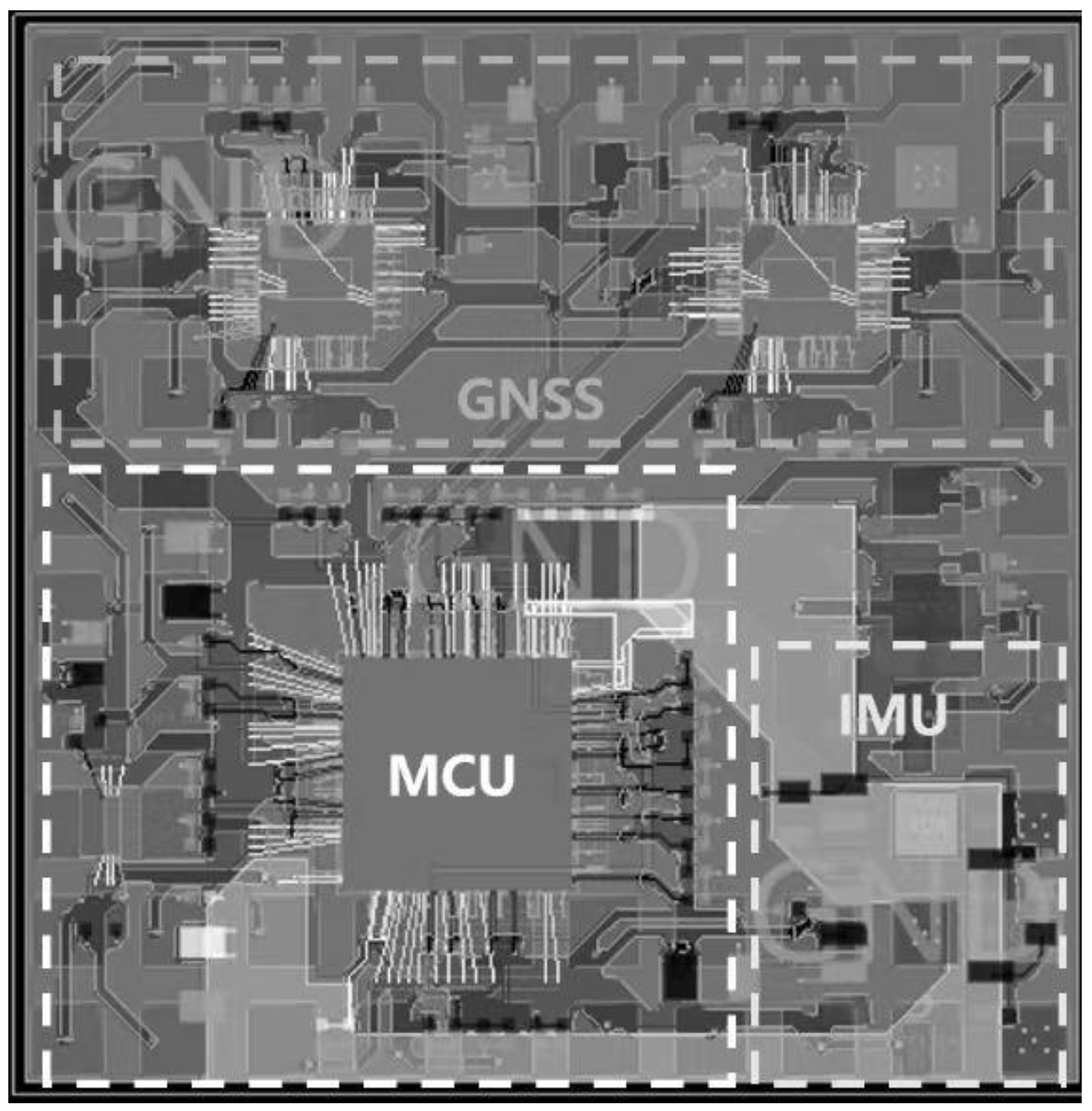
In order to further study the multi-physical coupling characteristics of system-in-package, a SiP chip for integrated navigation was designed in this study. Combined navigation systems include satellite navigation chips, inertial navigation chips, microprocessor chips, flash chips, and discrete devices [31,32]. This system-in-package allows a combined navigation system to be packaged into a single chip, resulting in reduced system size, lower power consumption, and ease of application; we named it a system-in-package combined navigation chip microsystem. This paper is organized as follows. In Section 2, the design of the microsystem is introduced, including signal transmission, packaging process, and substrate layout. Section 3 focuses on the simulation analysis of the designed microsystem. The performance of the microsystem was evaluated in terms of signal integrity, power integrity, and electrical-thermal-mechanical analysis. In Section 4, we fully analyze the coupling effects between the multi-physics. Finally, we summarize relevant data and propose a more comprehensive system-in-package design and simulation method.
3. Multi-Physics Simulation Analysis of the System-in-Package
After completing the package design, we imported the design file into the simulation software, which allowed us to perform electrical and thermal simulations of the designed package structure. Detailed simulation analyses are described below, and relevant simulation data are provided in the data file.
3.1. Signal Integrity
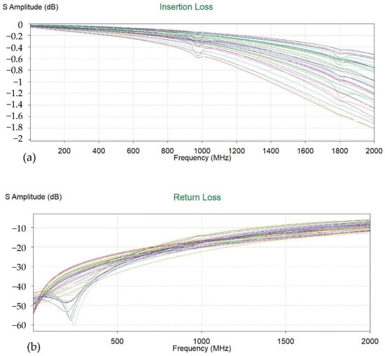
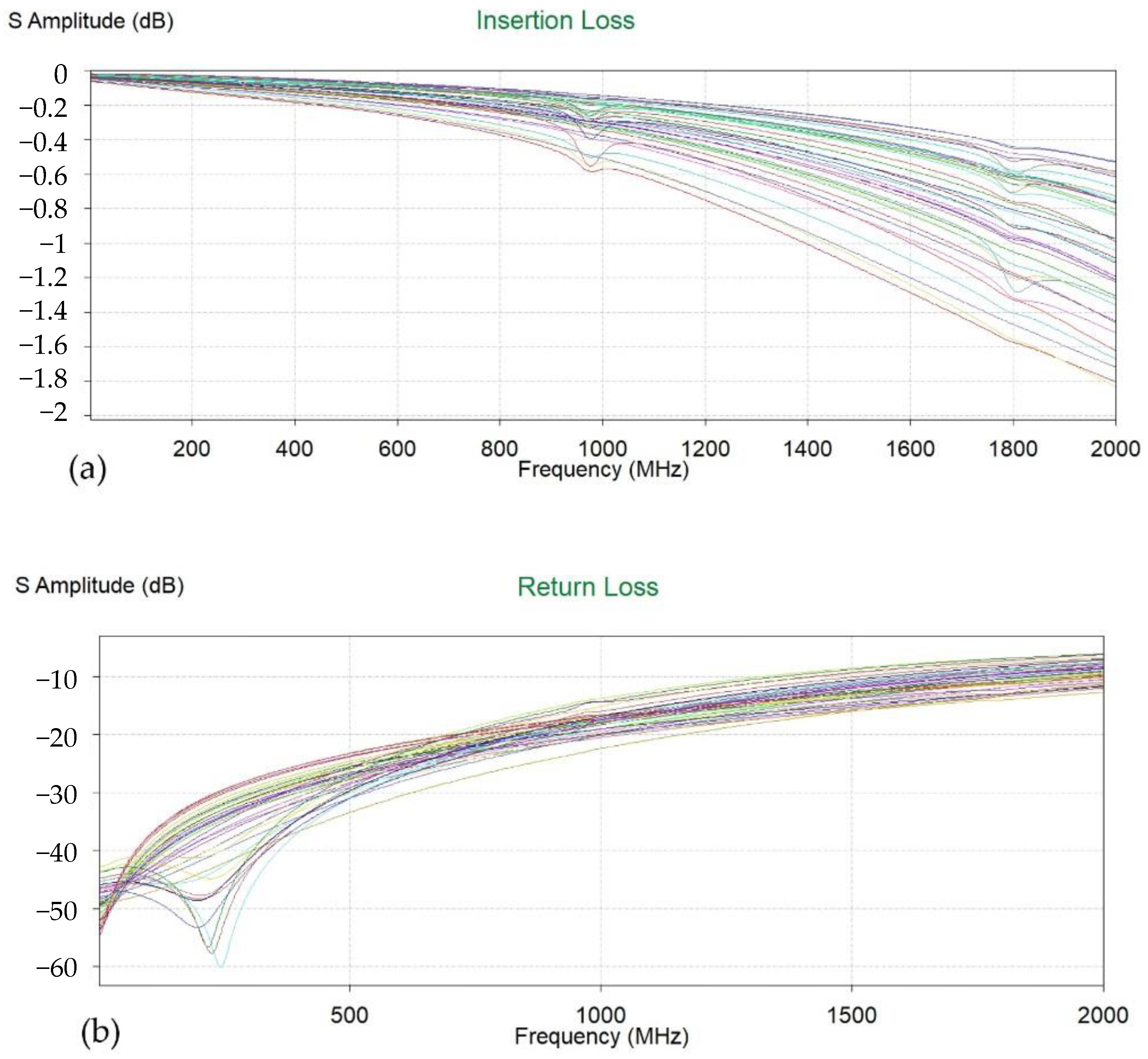
In this section, we analyze the signal integrity of the package design from multiple perspectives. In the entire design, the MCU section occupies the largest number of signals. Its maximum operating frequency is 1 GHz, and we focused on analyzing the insertion loss of its signal path within 2 GHz. As shown below in Figure 4a, we simulated that the insertion loss of all signal lines of the MCU was greater than −2 dB within 2 GHz. In Figure 4b, the return loss of all signal lines of the MCU was less than −20 dB within 500 MHz. These data mean that the MCU’s signal quality was guaranteed such that its signal speed was less than 10 MHz.
Figure 4.
The S-parameter of MCU signals. (a) Insertion loss. (b) Return loss. The different colored lines represent different signal channels.
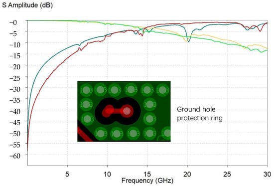
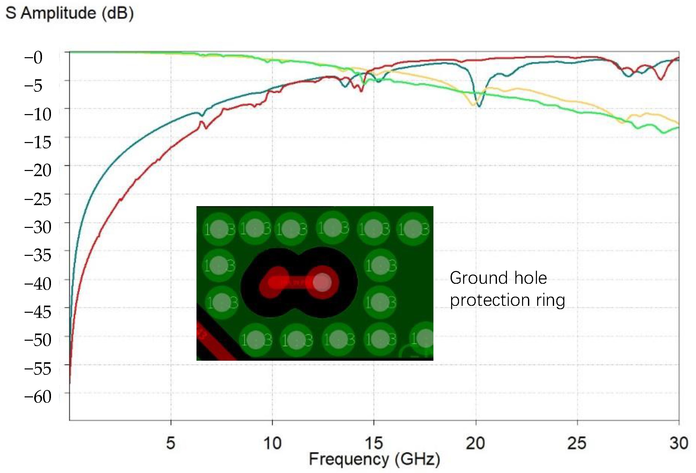
In addition, regarding the satellite navigation chip, there are two special RF signal inputs. We analyzed its S-parameters within 30 GHz. It was observed that above 5 GHz its return loss significantly deteriorated. Fortunately, however, the input signal operated at 1–2 GHz, and the S-parameters in this part performed well, as shown below in Figure 5. The insertion loss was greater than −1 dB@1 GHz and the return loss was less than −10 dB@1 GHz. It can be seen that the quality of the RF signal was significantly better than that of the MCU, because we added a ring of ground holes around the RF signal line to provide a close reflow loop, and also isolate interference, as shown in Figure 5. At the same time, the RF signal line was also designed to be as short as possible to obtain good S parameters.
Figure 5.
S-parameters of antenna signals. The red and blue lines represent the return loss, and the green and yellow lines represent the insertion loss.
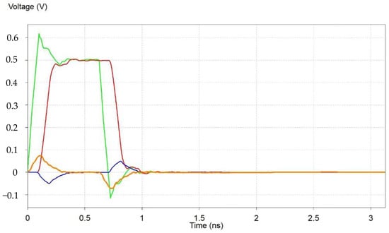
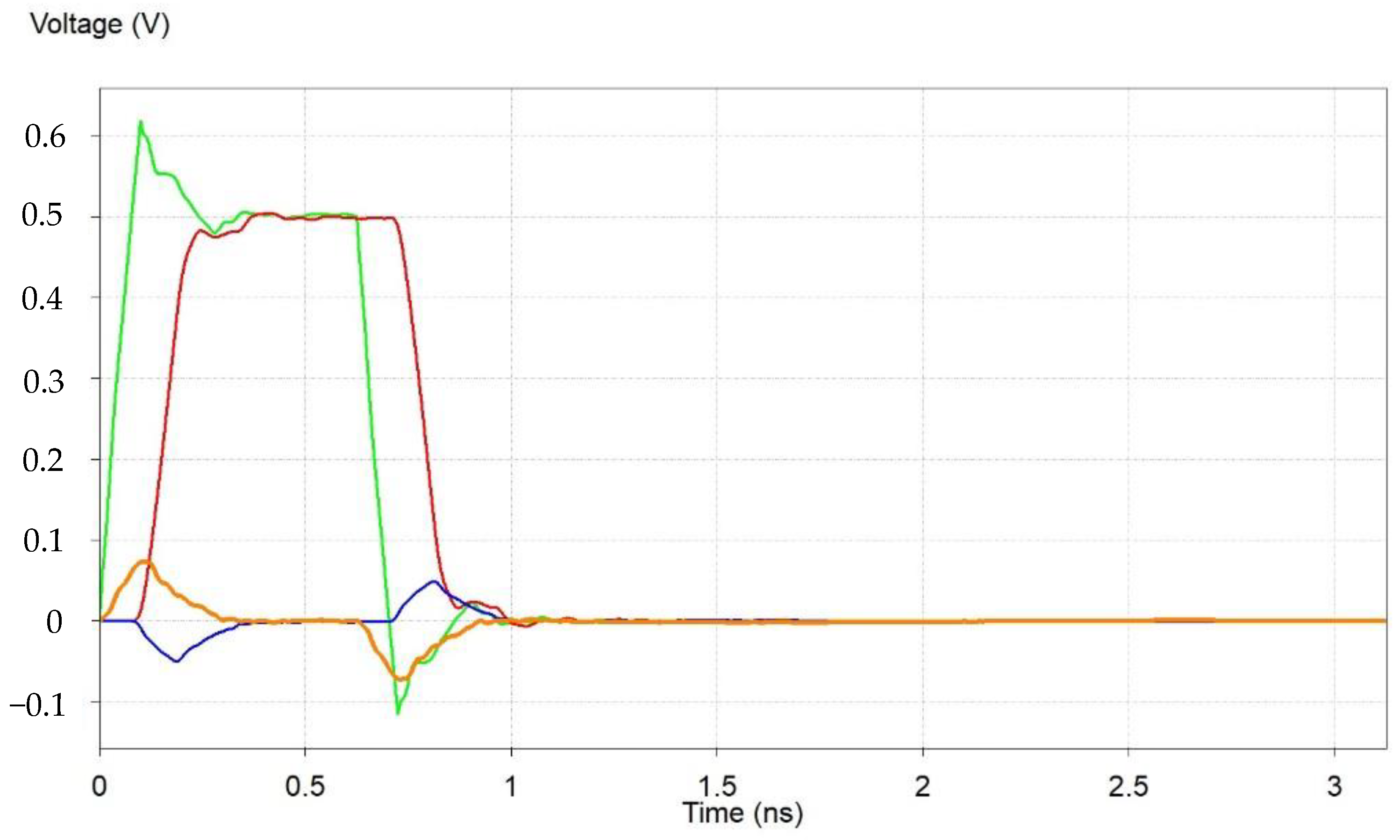
We further analyzed the time domain characteristics of the signal between the MCU and the IMU, and saw that the quality of the signal transmission was good. At the same time, we observed signal overshoot, as well as near-end and far-end signal noise. However, the amplitude of these noises was approximately 20% and did not produce logic errors, as shown below in Figure 6.
Figure 6.
Time domain transient simulation results of the signals between MCU and IMU. The green line represents the TX signal, the red line represents the RX signal, the blue line represents the FEXT signal, and the orange line represents the NEXT signal.
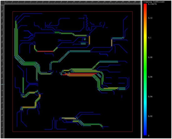
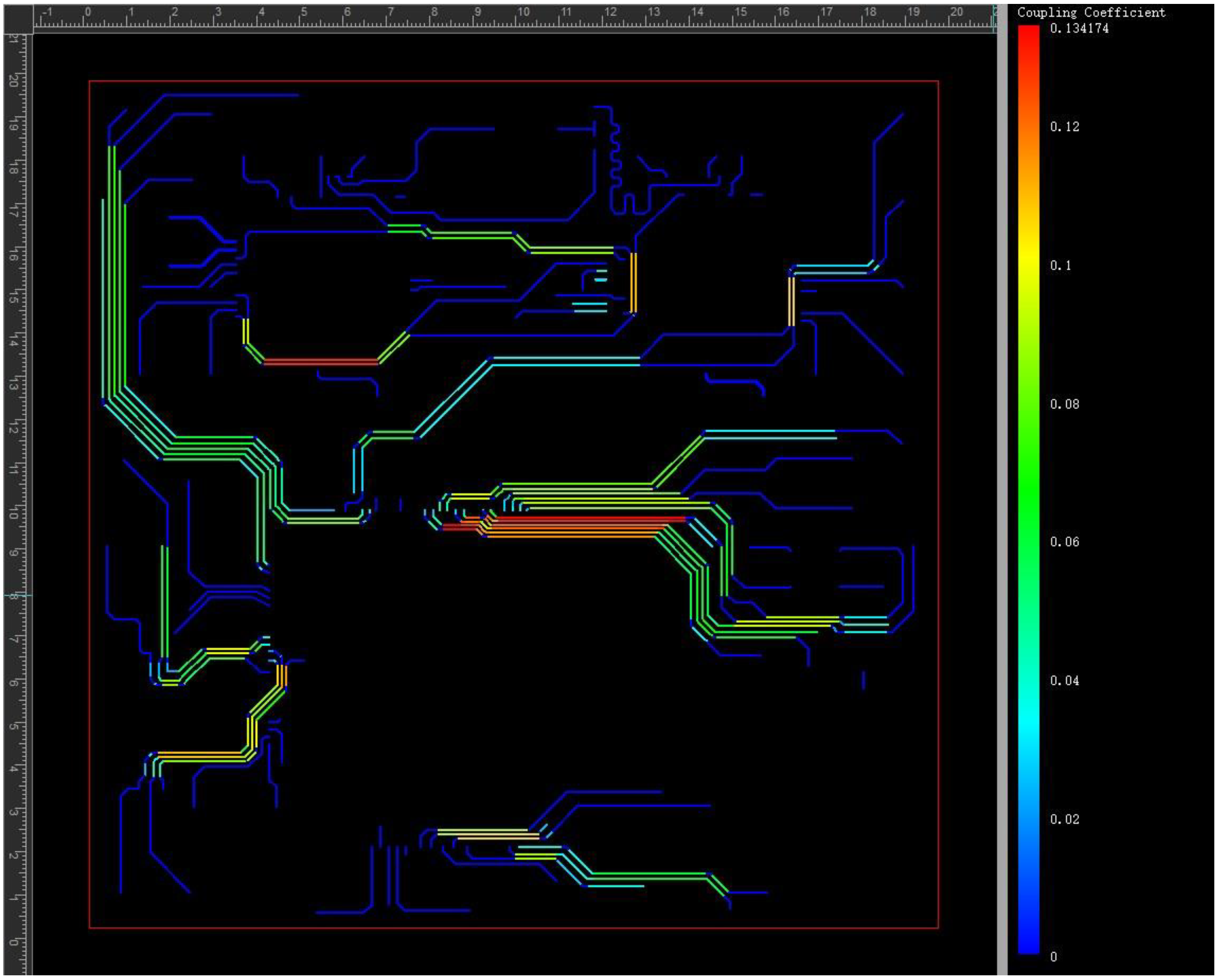
Figure 7, below, shows the coupling coefficient between the signal lines on the top surface, with a maximum value of 13.4174%. In the middle part of the layout, large coupling was caused by the small spacing of the signal lines. On the whole, such coupling is acceptable.
Figure 7.
Coupling distribution of top traces.
We conducted frequency domain or time domain analysis on multiple sets of data lines in the microsystem and they all met the working requirements, so it can be seen that the design meets signal integrity. The power supply performance of the microsystem is analyzed below.
3.2. Power Integrity
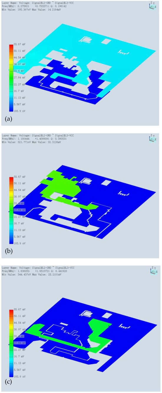
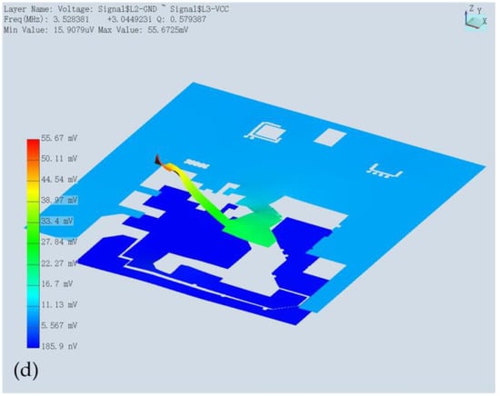
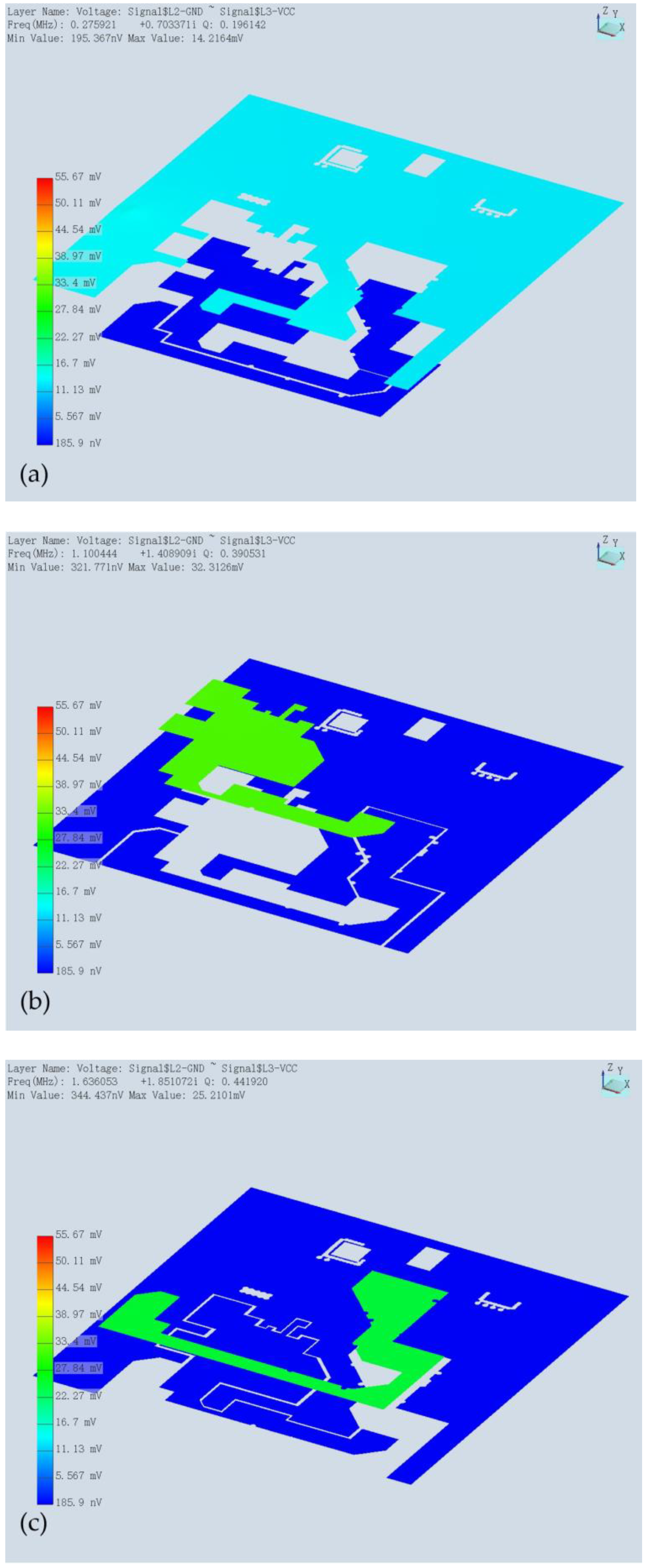
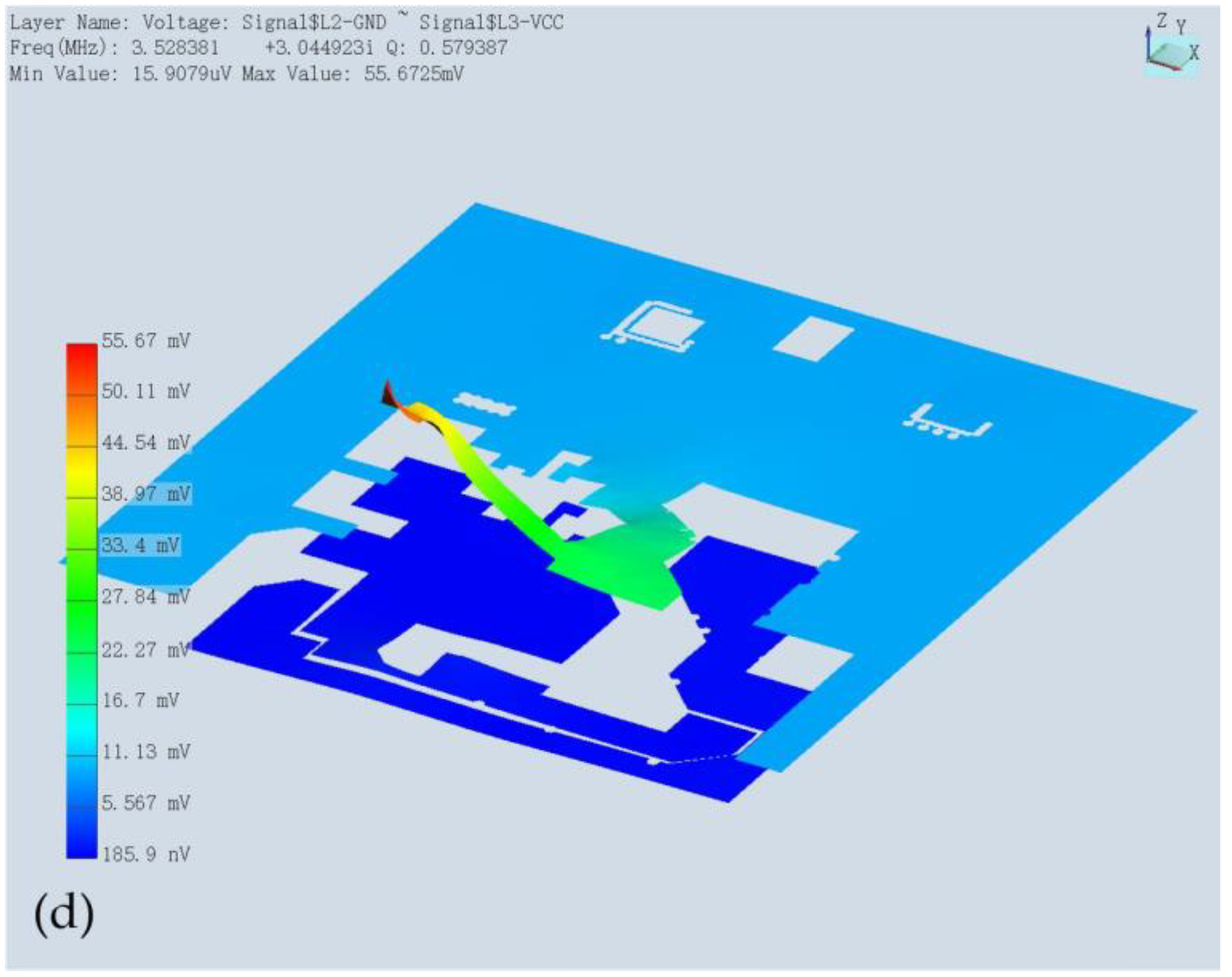
The good signal characteristics of SiP are shown above, and we further discuss its power integrity here. First, we analyzed the resonant characteristics of its power supply plane. Simulation results are shown below in Table 2, and we obtained nine resonant modes. The first three and last planar resonance diagrams are shown in Figure 8. The last five resonant modes all corresponded to the 3.3 V plane. The 9th mode yielded a maximum voltage value of 55 mV.
Table 2.
Resonant modes of the power plane.
Figure 8.
Resonance mode plots of the power plane. (a) First resonance. (b) Second resonance. (c) Third resonant. (d) Ninth resonance.
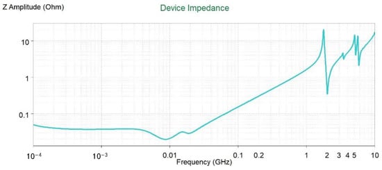
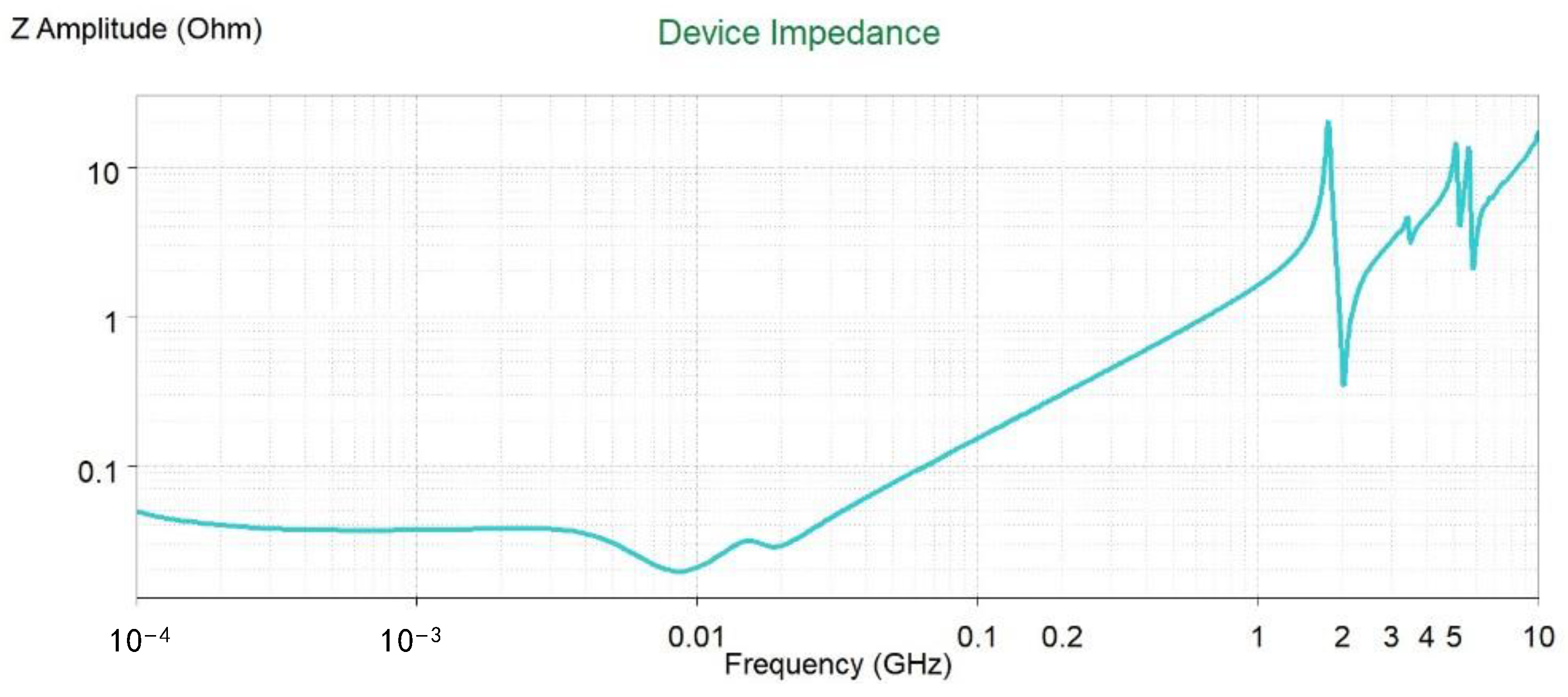
Further, we analyzed the impedance characteristics of a 1.8 V power supply at the MCU side. As can be seen below in Figure 9, before 500 MHz, its impedance was less than 1 Ω. There was a resonant front at high frequencies that could be further optimized using decoupling capacitors.
Figure 9.
The 1.8 V impedance curve of the MCU.
As shown above, the resonant noise of the power delivery network was small, and impedance characteristics were satisfied in the operating frequency. We also simulated the DC voltage drop characteristics of the power supply network, as shown in Table 3. All power delivery networks had a DC voltage drop of less than 2%, which met the requirements of the package design. In summary, the design of this microsystem is in line with power integrity requirements. In the following section, we discuss the electro-thermal-mechanical coupling analysis of the microsystem.
Table 3.
DC voltage drop characteristics of the power supply network.
3.3. Electrical-Thermal-Mechanical Analysis
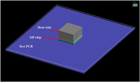
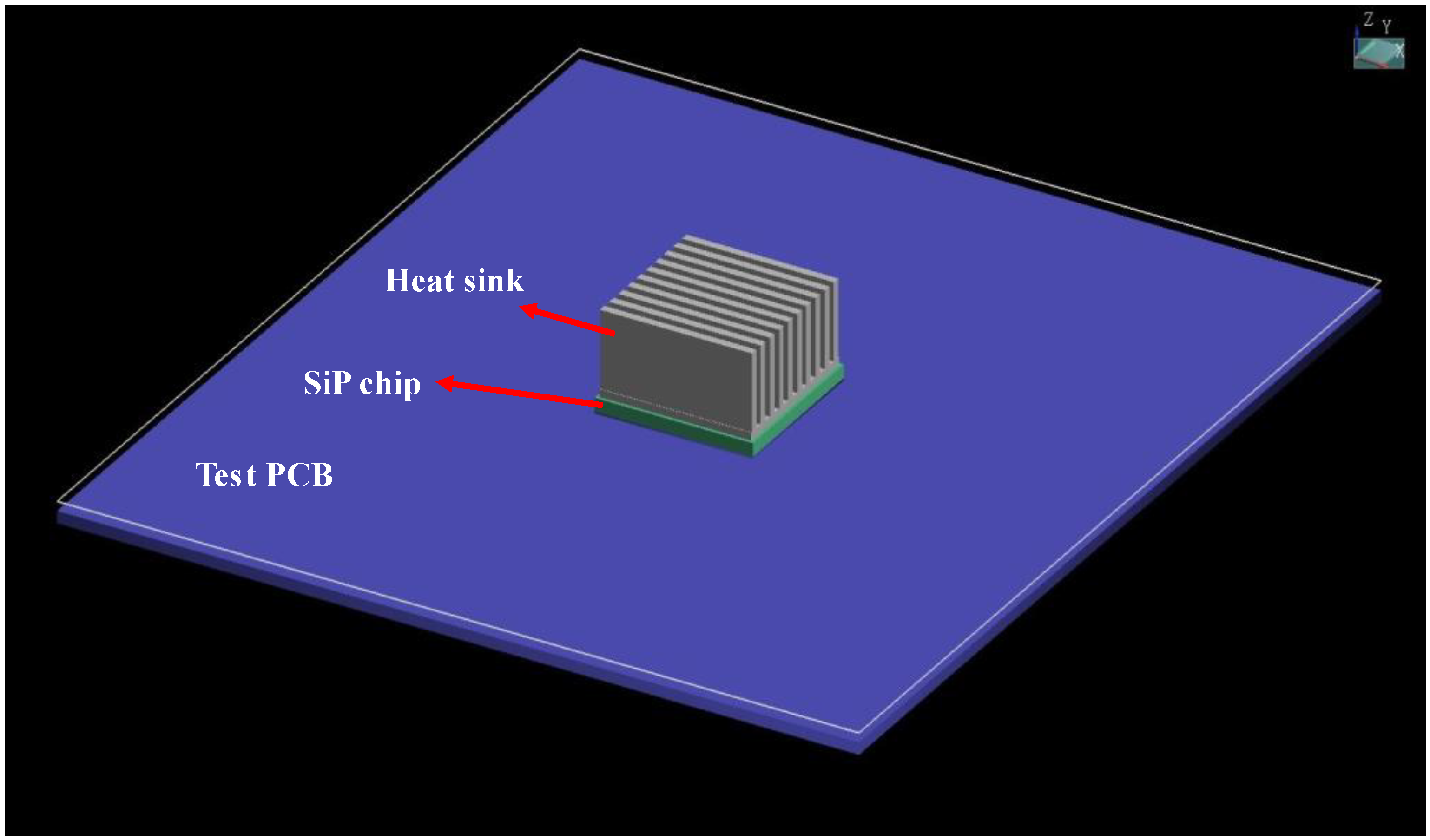
For system-in-package, the influence of temperature characteristics is important, so we performed an electro-thermal co-simulation, taking into account the effects of thermal stress, and at the same time were able to obtain results for three physics at once. We set up an analysis scenario, shown below in Figure 10, in which the SiP chip was mounted on a PCB test board with a heat dissipation structure at the bottom. The material and size parameters of the main components are shown in Table 4.
Figure 10.
Thermal analysis scenario.
Table 4.
Material and size parameters of key components.
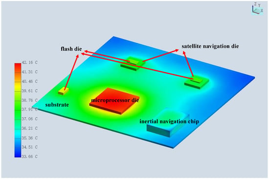
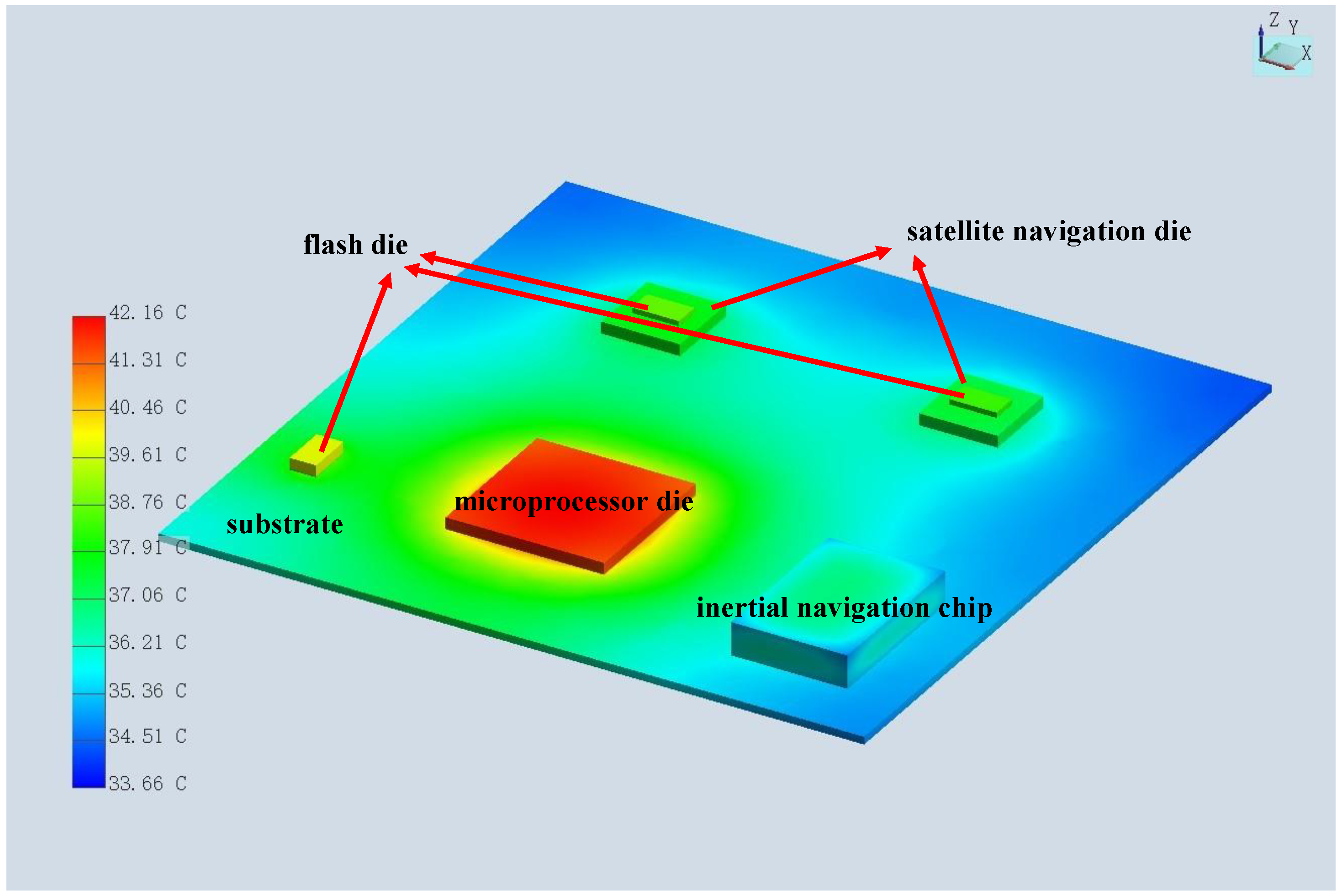
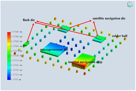
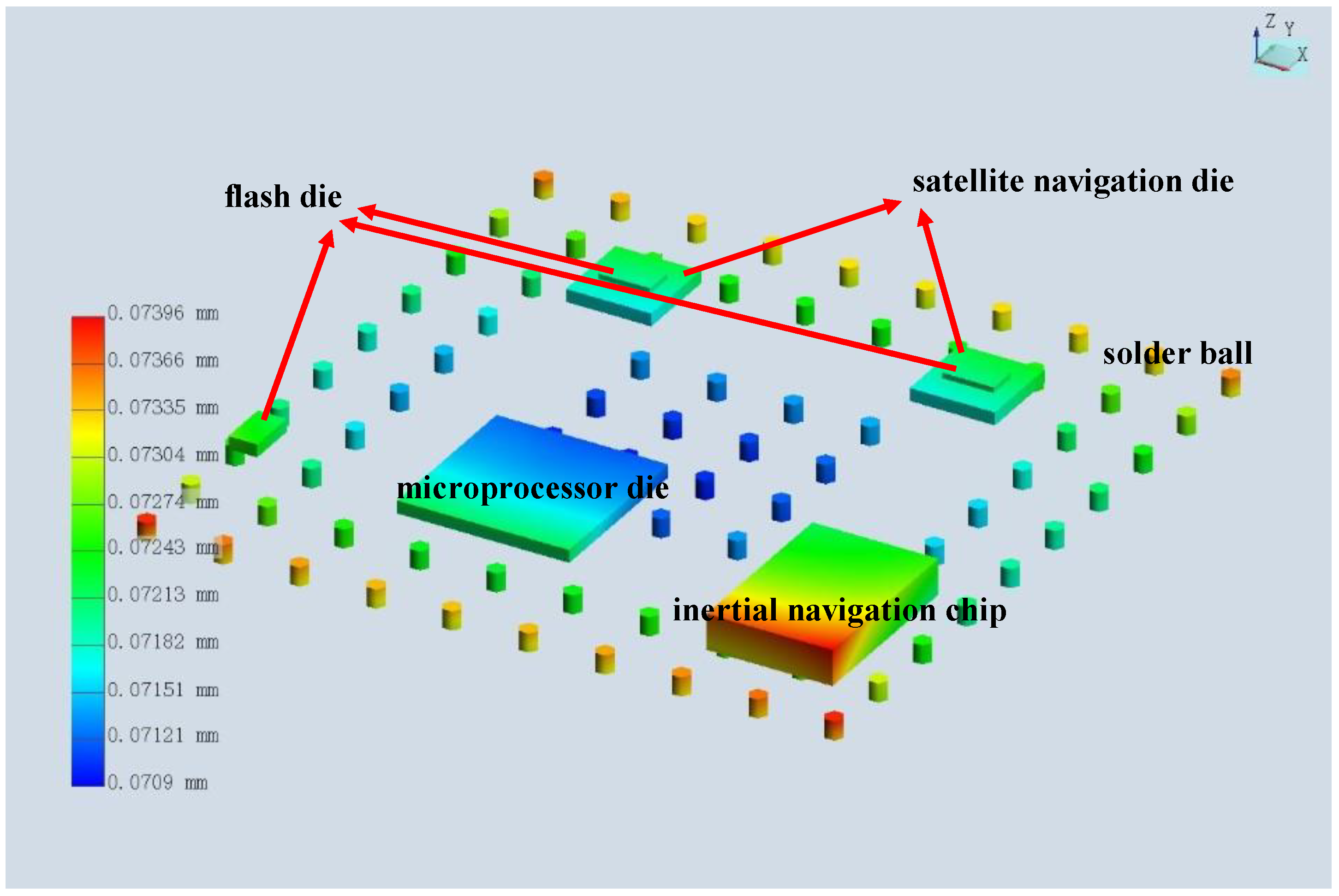
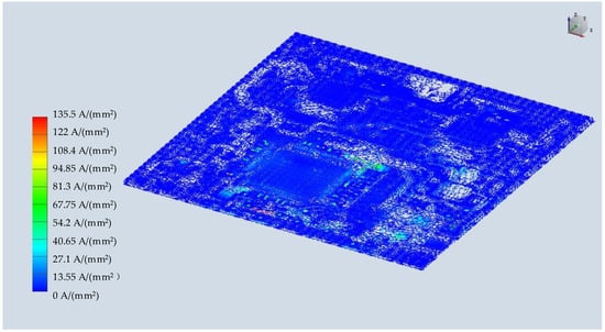
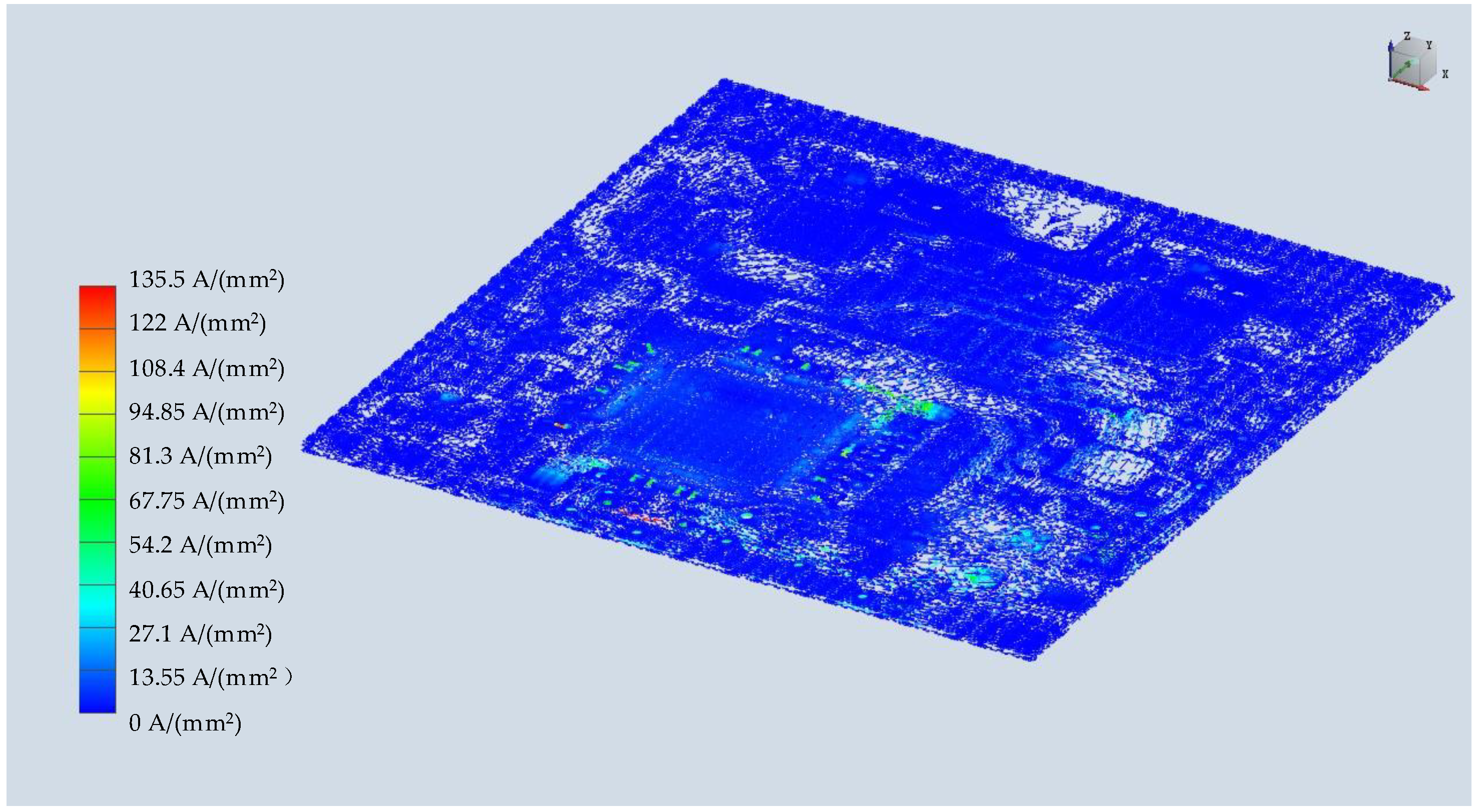
According to the actual chip power, the temperature distribution of this microsystem is shown below in Figure 11, and the highest temperature was in the MCU area because it has the highest power level. Due to mismatch in the coefficient of thermal expansion, the temperature caused warpage and thermal stress of the substrate. Therefore, we observed the largest displacement of pins (about 74 microns) in the four corners, as shown in the figure below. This was also the stress concentration area, which is prone to failure and was the focus area of design optimization, as shown below in Figure 12. At the same time, we obtained the current density results of the microsystem, as shown in Figure 13, in which it can be observed that the current density was higher in the narrower power plane.
Figure 11.
Temperature distribution of the system.
Figure 12.
Warpage of the system due to thermal stress.
Figure 13.
Current density distribution of the system.
4. Discussion
In this paper, we systematically discuss our microsystem design and simulation methods. Simulation results show that shortening the length of the signal line and increasing the ground hole wraparound significantly increased the transmission quality of the signal lines. Widening the connecting lines of the power supply network reduced the DC voltage drop, and the division of the power supply plane affected its resonant mode. The temperature distribution was mainly caused by the chip power; therefore, temperature-sensitive devices should be kept away from high-power devices. Stress warpage results show that solder joints at the corners of the microsystem were subjected to the most severe deformation, and that signal lines should be avoided and used as redundant grounding.
5. Conclusions
This article describes how to design and simulate a system-in-package microsystem. We obtained adequate results during simulation analysis of signal integrity, power integrity, and thermal analysis. Critical signals, such as MCU signals, antennas’ RF signals, and signals between MCUs and IMUs, are required for microsystem operation. Analysis of the resonance characteristics and impedance characteristics of the power supply plane also showed satisfactory results. Thermal analysis showed that the reliability of the system is guaranteed.
Supplementary Materials
The following supporting information can be downloaded at: https://www.mdpi.com/article/10.3390/mi15020167/s1, Table S1: Data of figures.
Author Contributions
Data analysis of the modelling simulation and writing—original draft preparation, Y.Y.; formal analysis and writing—review and editing, G.S.; supervision and writing—review and editing, Y.J. All authors have read and agreed to the published version of the manuscript.
Funding
This work was supported by the Shenzhen Science and Technology Innovation Commission under Grant KQTD20200820113105004.
Data Availability Statement
Data are contained within the article and supplementary materials.
Conflicts of Interest
The authors declare no conflicts of interest. The funders had no role in the design of this study; in the collection, analyses, or interpretation of data; in the writing of this manuscript; or in the decision to publish results.
References
- He, L.; Elassaad, S.; Shi, Y.; Hu, Y.; Yao, W. System-in-Package: Electrical and Layout Perspectives. Found. Trends® Electron. Des. Autom. 2010, 4, 223–306. [Google Scholar] [CrossRef] [Scilit]
- Meyer, J. System in Package Design Case Study. Addit. Conf. Device Packag. HiTEC HiTEN CICMT 2015, 2015, 973–994. [Google Scholar] [CrossRef] [Scilit]
- Hu, Y.C.; Liang, Y.M.; Hu, H.P.; Tan, C.Y.; Shen, C.T.; Lee, C.H.; Hou, S.Y. CoWoS Architecture Evolution for Next Generation HPC on 2.5D System in Package. In Proceedings of the 2023 IEEE 73rd Electronic Components and Technology Conference (ECTC), Orlando, FL, USA, 30 May–2 June 2023; pp. 1022–1026. [Google Scholar]
- Fang, Z.; Wu, B. Integrating High Frequency Radar Chip Using Laminated Substrate Transitions for System-In-Package Design. In Proceedings of the 2023 China Semiconductor Technology International Conference (CSTIC), Shanghai, China, 26–27 June 2023; pp. 1–3. [Google Scholar]
- Bocca, A.; Macii, A. Thermal modeling and analysis of a power ball grid array in system-in-package technology. Multiscale Multidiscip. Model. Exp. Des. 2022, 5, 31–41. [Google Scholar] [CrossRef] [Scilit]
- Kim, G.; Lim, D.; Lee, J.; Chang, I.; Pak, J.S.; Cho, Y.; Im, Y. Impact of System-in-Package in side-by-side discrete SoC-DRAM configurations on SI, PI and thermal performance. In Proceedings of the 2021 IEEE 71st Electronic Components and Technology Conference (ECTC), San Diego, CA, USA, 1 June–4 July 2021; pp. 1805–1811. [Google Scholar]
- Ali, M.; Hassan, A.; Honarparvar, M.; Nabavi, M.; Audet, Y.; Sawan, M.; Savaria, Y. A Versatile SoC/SiP Sensor Interface for Industrial Applications: Implementation Challenges. IEEE Access 2022, 10, 24540–24555. [Google Scholar] [CrossRef] [Scilit]
- Oukaira, A.; Said, D.; Mellal, I.; Ettahri, O.; Zbitou, J.; Lakhssassi, A. Thermal camera for System-in-Package (SiP) technology: Transient thermal analysis based on FPGA and Finite Element Method (FEM). AEU Int. J. Electron. Commun. 2023, 172, 154980. [Google Scholar] [CrossRef] [Scilit]
- Fruehauf, P.; Munding, A.; Pressel, K.; Vogt, M.; Schwarz, P. Chip-package-board reliability of System-in-Package using laminate chip embedding technology based on Cu leadframe. In Proceedings of the 2018 7th Electronic System-Integration Technology Conference (ESTC), Dresden, Germany, 18–21 September 2018; pp. 1–7. [Google Scholar]
- Chen, Z.; Feng, Z.; Ruan, M.; Xu, G.; Liu, L. Effects of Moisture Diffusion on a System-in-Package Module by Moisture-Thermal-Mechanical-Coupled Finite Element Modeling. Micromachines 2022, 13, 1704. [Google Scholar] [CrossRef] [Scilit] [PubMed]
- Wang, W.; Liu, Y.; Zhao, Z.; Zhou, H. Parallel Multiphysics Simulation of Package Systems Using an Efficient Domain Decomposition Method. Electronics 2021, 10, 158. [Google Scholar] [CrossRef] [Scilit]
- Wu, X.; Cao, M.; Shan, G.; Yang, Y. A Fast Analysis Method of Multiphysics Coupling for 3-D Microsystem. IEEE Trans. Comput. -Aided Des. Integr. Circuits Syst. 2022, 41, 2372–2379. [Google Scholar] [CrossRef] [Scilit]
- Lee, H.; Im, Y.; Shin, Y. Comparative Study Of 3D Package Configurations in Power Delivery and Thermal Perspective. In Proceedings of the 2018 International Wafer Level Packaging Conference (IWLPC), San Jose, CA, USA, 23–25 October 2018; pp. 1–7. [Google Scholar]
- You, S.-H.; Jeon, S.; Oh, D.; Kim, K.; Kim, J.; Cha, S.-Y.; Kim, G. Advanced Fan-Out Package SI/PI/Thermal Performance Analysis of Novel RDL Packages. In Proceedings of the 2018 IEEE 68th Electronic Components and Technology Conference (ECTC), San Diego, CA, USA, 29 May–1 June 2018; pp. 1295–1301. [Google Scholar]
- Xia, S.; Dogruoz, B.M.; Wang, Y.; Wu, S.; Bai, S.; Hwang, C.; Wu, Z. A Thermal-aware DC-IR Drop Analysis for 2.5D IC. In Proceedings of the 2023 IEEE Symposium on Electromagnetic Compatibility & Signal/Power Integrity (EMC + SIPI), Grand Rapids, MI, USA, 29 July–4 August 2023; pp. 670–675. [Google Scholar]
- Kim, S.K.; Oh, D.S.; Hwang, S.; Lee, B.W.; Cha, S.Y.; Kim, T.H. Electrical and Thermal Co-Analysis of Thermally Efficient SiP for High Performance Applications. In Proceedings of the 2019 Electrical Design of Advanced Packaging and Systems (EDAPS), Kaohsiung, Taiwan, 16–18 December 2019; pp. 1–3. [Google Scholar]
- Yu, D.; Wang, H.; Xu, J. Impact of Worst-Case Excitation for DDR interface Signal and Power Integrity Co-Simulation. J. Electron. Test. 2020, 36, 365–374. [Google Scholar] [CrossRef] [Scilit]
- George, S.S.; Sivanantham, S.; Manikant Ch, S.S. Design strategies for Signal Integrity, Power Integrity and EMI EMC issues in Computing boards and Systems. In Proceedings of the 2023 Joint Asia-Pacific International Symposium on Electromagnetic Compatibility and International Conference on ElectroMagnetic Interference & Compatibility (APEMC/INCEMIC), Bengaluru, India, 22–25 May 2023; pp. 1–4. [Google Scholar]
- George, S.S.; Sivanantham, S.; Pawar, S.; Vikram, R. Signal Integrity and Power Integrity Challenges in Embedded Computing Boards. In Proceedings of the 2018 15th International Conference on ElectroMagnetic Interference & Compatibility (INCEMIC), Bengaluru, India, 13–16 November 2018; pp. 1–4. [Google Scholar]
- Petrosyants, K.O.; Ryabov, N.I. Quasi-3D Thermal Simulation of Integrated Circuit Systems in Packages. Energies 2020, 13, 3054. [Google Scholar] [CrossRef] [Scilit]
- Oukaira, A.; Said, D.; Zbitou, J.; Lakhssassi, A. Transient Thermal Analysis of System-in-Package Technology by the Finite Element Method (FEM). In Proceedings of the 2022 International Conference on Microelectronics (ICM), Casablanca, Morocco, 4–7 December 2022; pp. 30–33. [Google Scholar]
- Pan, S.H.; Chang, N.; Hitomi, T. 3D-IC dynamic thermal analysis with hierarchical and configurable chip thermal model. In Proceedings of the 2013 IEEE International 3D Systems Integration Conference (3DIC), San Francisco, CA, USA, 2–4 October 2013; pp. 1–8. [Google Scholar]
- Oukaira, A.; Said, D.; Zbitou, J.; Lakhssassi, A. Advanced Thermal Control Using Chip Cooling Laminate Chip (CCLC) with Finite Element Method for System-in-Package (SiP) Technology. Electronics 2023, 12, 3154. [Google Scholar] [CrossRef] [Scilit]
- Tsai, M.Y.; Liu, C.M.; Wang, Y.W.; Liu, H.Y. Effects of Metal Frame and Adhesive on Thermally-Induced Warpage and Stress of 2.5D Packages: Experimental and Numerical Studies. IEEE Trans. Device Mater. Reliab. 2018, 18, 450–455. [Google Scholar] [CrossRef] [Scilit]
- Rajmane, P.; Dhandapani, K.; Schwarz, M.; Syed, A. Investigation of the Factors Affecting the Warpage Prediction of Multi-Chip Package. In Proceedings of the 2021 IEEE 71st Electronic Components and Technology Conference (ECTC), San Diego, CA, USA, 1 June–4 July 2021; pp. 1514–1520. [Google Scholar]
- Hsu, J.; Yang, A.; Jeong, Y.; Ahn, B.; Koyama, T.; Oi, K.; Lee, J.; Horie, T.; Tsuriya, M. SiP module warpage characterization and simulation study. In Proceedings of the 2018 International Conference on Electronics Packaging and iMAPS All Asia Conference (ICEP-IAAC), Mie, Japan, 17–21 April 2018; pp. 7–12. [Google Scholar]
- Zhang, K.; Lin, V.; Lai, D.; Wang, Y.P. Warpage and Stress Simulation Analysis of Substrate on Substrate Antenna in Package (AiP) for 5G CPE Application. In Proceedings of the 2022 International Conference on Electronics Packaging (ICEP), Sapporo, Japan, 11–14 May 2022; pp. 197–198. [Google Scholar]
- Yan, Z.; Zhong, C.; Lou, L.; Yu, S.; Hu, Z.; Sun, R. Warpage Simulation and Analysis for FOWLP with Metal Carrier. In Proceedings of the 2022 23rd International Conference on Electronic Packaging Technology (ICEPT), Dalian, China, 10–13 August 2022; pp. 1–6. [Google Scholar]
- Niu, Y.; Wang, W.; Wang, Z.; Dhandapani, K.; Schwarz, M.; Syed, A. Warpage Variation Analysis and Model Prediction for Molded Packages. In Proceedings of the 2019 IEEE 69th Electronic Components and Technology Conference (ECTC), Las Vegas, NV, USA, 28–31 May 2019; pp. 819–824. [Google Scholar]
- Lee, K.; Kim, M.S.; Kim, J.; Kim, S.; Lee, D.; Jung, K. Improvement of package warpage through substrate and EMC optimization. In Proceedings of the 2018 China Semiconductor Technology International Conference (CSTIC), Shanghai, China, 11–12 March 2018; pp. 1–4. [Google Scholar]
- Yan, P.; Jiang, J.; Tang, Y.; Zhang, F.; Xie, D.; Wu, J.; Liu, J.; Liu, J. Dynamic Adaptive Low Power Adjustment Scheme for Single-Frequency GNSS/MEMS-IMU/Odometer Integrated Navigation in the Complex Urban Environment. Remote Sens. 2021, 13, 3236. [Google Scholar] [CrossRef] [Scilit]
- Wang, C.; Chen, X.; Zhang, N.; Wang, J.; Jiao, Z.; Zhong, Y. Research on the Algorithm of Combined GNSS/SINS Navigation System based on Adaptive UKF. In Proceedings of the 2023 IEEE 6th International Conference on Electronic Information and Communication Technology (ICEICT), Qingdao, China, 21–24 July 2023; pp. 535–540. [Google Scholar]



Disclaimer/Publisher’s Note: The statements, opinions and data contained in all publications are solely those of the individual author(s) and contributor(s) and not of MDPI and/or the editor(s). MDPI and/or the editor(s) disclaim responsibility for any injury to people or property resulting from any ideas, methods, instructions or products referred to in the content. |
© 2024 by the authors. Licensee MDPI, Basel, Switzerland. This article is an open access article distributed under the terms and conditions of the Creative Commons Attribution (CC BY) license (https://creativecommons.org/licenses/by/4.0/).