


Abstract
The transition to clean photovoltaic sustainable generation sources has motivated several developments in required power electronics interface systems. The conventional solution is based on two cascaded conversion stages, leading to reduced efficiency, inevitable leakage currents, and/or a high number of required components. Another solution is the use of integrated two-stage solutions suffering from asymmetrical switch structures, discontinuous input side currents, and/or complex modulation and control requirements. This paper presents a modified configuration with symmetrical six switches based on the common ground boost inverter solution. Furthermore, the proposed solution presents a continuous input side current and a simple modulation strategy. Moreover, the proposed CG topology offers a reduction of the current stress on the power switch by diverting the load current away from the power switch during the inductor charging. The operation, modulation, and control of the developed solution are presented in the paper, including comprehensive performance comparisons with boost inverter solutions in the literature. Simulation and experimental prototype-based results confirm the advantages and superiority of the proposed topology over existing topologies.
1. Introduction
The transition to clean and environmentally friendly sustainable energy solutions, especially in power generation and transportation sectors, has brought different motivations to developing efficient power electronic solutions [1]. Power electronic conversion systems represent a crucial element in photovoltaic (PV) generation as the highest contributing renewable source in global records [2,3]. Power electronics DC–DC converters based on isolated solutions have been reviewed in [4]. The conventional solution for integrating PV systems with this utility is the cascaded boost inverter with a two-level inverter system [5]. This configuration enables the separation of control objectives among the two converters and facilitates the extraction of maximum power (MP) on the DC side and the injection of high-quality current on the AC side [6]. The control of this configuration is crucial in hybrid PV with energy storage systems [7,8]. However, this solution does not afford maximum efficiency to many of the required components [9,10]. Moreover, this configuration has inevitable common mode voltages (CMVs) due to the switching modulation of different semiconductor switches [11]. The CMVs with the stray capacitances between the PV panels and the earth generate leakage currents in the PV systems, which affect humans and equipment [12]. Furthermore, grid codes have set a limit for the permissible generated leakage currents in PV systems [13].
Several topologies and modulation schemes have been presented in the literature for the reduction of resulting leakage currents in PV systems [14]. Some methods are based on modulation techniques [15], including space-vector modulation [16]. A space vector modulation has been presented for leakage current reduction in induction motor drives in [17] with a parallel configuration of full-bridge converters. An improved over-modulation scheme for suppressing common-mode voltages and, hence, reducing leakage current has been proposed in [18] for three-level NPC inverter systems. However, these methods need complex calculations and face some limitations in several topologies, in addition to their inability to fully mitigate leakage currents. The increasing number of components and requirements of complex control and modulation strategies hinder the widespread adoption of leakage-current-reduction topologies in the literature [19]. Moreover, they may not be able to totally eliminate leakage currents [20]. The modulation schemes developed for leakage current reduction possess asymmetrical switching schemes and topology structures [21]. Among the presented methods, the common ground (CG) PV inverter topologies [22], also named double-grounded (DG) inverters, have found broad interest [23]. The CG-based topologies include a direct connection between the neutral wire of the grid side and the negative wire of the PV panel side [24]. This, in turn, provides a zero CMV at all operating conditions, leading to the total elimination of existing leakage current components [25].
A topology based on the virtual DC-link bus has been developed in [26]. A switched capacitor cell is used to generate the negative voltage level, while it is mainly charged during positive voltage level generation [27]. Another topology using the charge pump concept has been presented in [28]. The current stress on some switches can be considered a relative disadvantage; however, it can be mitigated through appropriate design methodologies. Another charge-pump circuit concept was introduced in [29], but the two-stage charge transfer mechanism significantly increases the number of required power components. A notable inverter with a common ground configuration was proposed in [30], featuring a reduced switch count and utilizing a unipolar pulse-width modulation (PWM) strategy. Additionally, a multi-level common ground transformerless inverter was presented in [31], which eliminates the need for switched capacitors. This topology offers a lower switch count compared to conventional designs but requires a higher input voltage compared to full-bridge-based topologies.
The topology proposed in [32] introduces a straightforward and practical approach by integrating the boost converter and single-phase inverter within a common ground configuration, effectively mitigating leakage current. However, one of the power switches experiences significant current stress due to the combined flow of load current and input current through the boost switch. Additionally, a prominent feature of modern boost inverters is the reliance on half-bridge configurations. Consequently, this paper proposes a CG boost inverter design with symmetrical switches, aiming at reducing current stress and enhancing the efficiency of generation systems.
A seven-level, three-fold boosting of a low input voltage CG inverter has been presented in [33]. The presented topology can achieve three times the voltage gain while eliminating leakage currents. However, the topology employs ten power switches, a diode, and two capacitors. Furthermore, the topology uses asymmetrical components due to the different voltages of DC capacitors. Another solution has been presented in [34] for reducing component voltage stresses and reducing the number of components. However, the presented solution suffers from the discontinuous DC input side current, which affects the PV side current stresses and its MPPT control. Another topology based on zeta inverter using non-electrolytic capacitors has been presented in [35]. Similarly, the topology has a discontinuous DC input side current problem. Another topology has been provided in [36] using only four power switches, a single inductor, and a single virtual DC capacitor. The topology offers a solution for the discontinuous DC input side current problem. However, the virtual DC capacitor has a high degree of ripple and is difficult to control.
In [37], a new nine-level CG topology has been presented. The topology uses eight power switches, two power diodes, and two virtual DC link capacitors. Another topology based on a reduced number of power switches has been presented in [38] using a flying inductor principle. However, the inductor current stresses are very high, and the inductor contains a high AC component. A topology with only three power switches has been proposed in [39]. However, the topology employs six diodes, two inductors, and three DC capacitors. Furthermore, the topology provides a discontinuous input side current.
It is clear from the above discussion that the majority of existing topologies suffer from an increased number of components and/or present a discontinuous input-side current. Further modifications and improvements of topologies are essential with CG connections. Moreover, reducing the number of employed components and maintaining a symmetrical device structure is crucial for industrializing CG inverters. Stimulated by these critical issues, this paper provides a new CG inverter topology that offers the following benefits:
- The proposed topology provides similar performance to split source inverter topology while preserving lower current stress for the connected power switch to the boost inductor. In addition, the proposed topology possesses the common ground configuration/connection; thus, the leakage current is eliminated.
- The proposed topology employs symmetrical power switches with complementary pulses using half-bridge modules with a simultaneous operation. Employing available half-bridge modules enables straightforward implementation with minimal additional design effort.
- The proposed topology uses a simpler approach for signals generator by using hybrid sinusoidal and constant PWM, providing a constant duty cycle to control the charging and discharging of boosting inductor .
The remaining sections of the paper are organized as follows: Section 2 presents the new proposed circuit and its operating modes. The voltage gain and PWM generation for the newly proposed topology are given in Section 3. The obtained simulation and experimental prototype results are provided in Section 4, enhanced with performance comparisons of the proposed topology and existing CG solutions in the literature in Section 5. Section 6 provides dynamical closed-loop simulation results of the proposed topology. Finally, the conclusions of the paper are provided in Section 7.
2. Proposed CG Boost Inverter
2.1. Zero-Leakage Current PV Inverter Topology
The recent advancements in transformerless inverter (TLI) topologies for PV applications have made them preferred solutions. TLIs possess higher power densities compared to transformer-based solutions, as well as having smaller sizes, and lower costs. A significant issue with TLIs is the leakage currents resulting from parasitic capacitances between the metal parts of the panel and the ground. The amount of leakage currents is a function of the common-mode voltages resulting from the power electronic conversion stages.
A perfect solution to completely eliminate leakage currents in PV systems is through specific topologies and/or modulation techniques that maintain the CMV constant or equal to zero. Therefore, the amount of leakage current is completely eliminated in PV systems. Among the various presented solutions, the common ground (CG)-based power inverter solutions have shown superior performance and power quality, with zero leakage current and high efficiency. The CG topologies are also referred to as doubly grounded (DG) topologies.
Inherently, the CG solutions possess a direct connection between the negative PV side terminal and the neutral side terminal of the grid. Consequently, the common-mode voltage remains constant during operation, and the parasitic capacitance between the PV array and ground is not excited by high-frequency switching components. As a result, leakage current is inherently eliminated by structure, consistent with the operating principle of common-ground transformerless inverters reported in the literature [21,40].
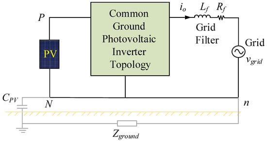
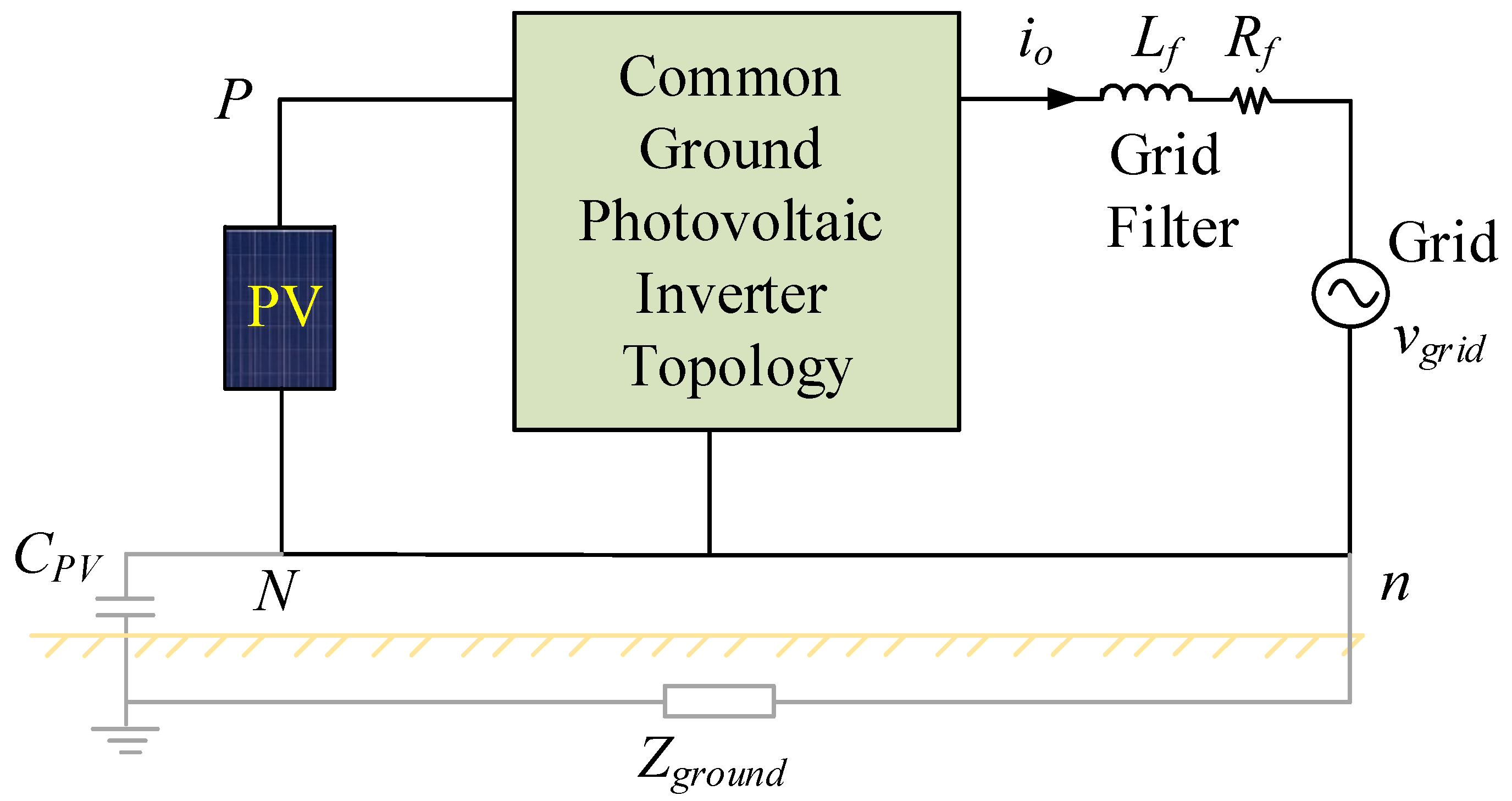
A generalized representation of the CG concept is shown in Figure 1. The circuit includes the parasitic capacitance () connected between the negative port of the PV panels and the neutral point of the AC port [12]. In addition, the ground impedance () is included in the circuit equivalent model. With this connection, it is ensured that the CMV, the primary cause of leakage current, remains constant without requiring high switching components. With the inclusion of the direct CG short-circuit in the configuration, the modeled impedance and capacitance are clamped, resulting in the cancellation of the expected ground leakage current components accordingly. Therefore, zero leakage current components are obtained through employing the TLI based on the CG configuration.
Figure 1.
Principle of zero leakage current PV inverter topology.
2.2. Development of Proposed CG Topology
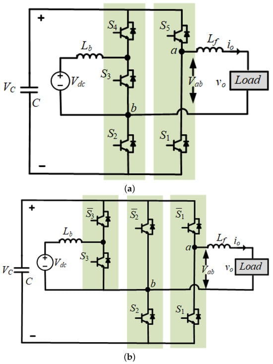
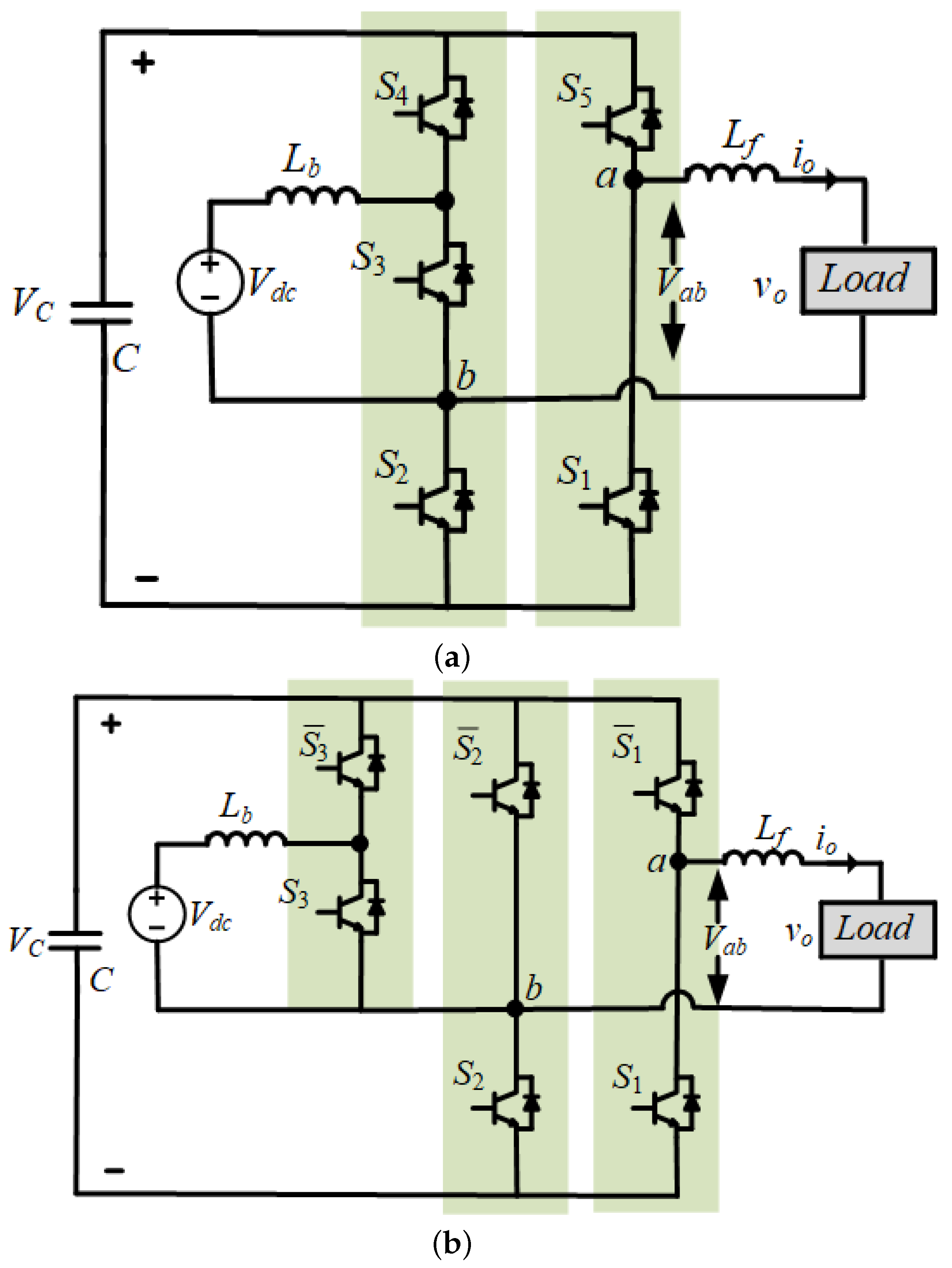
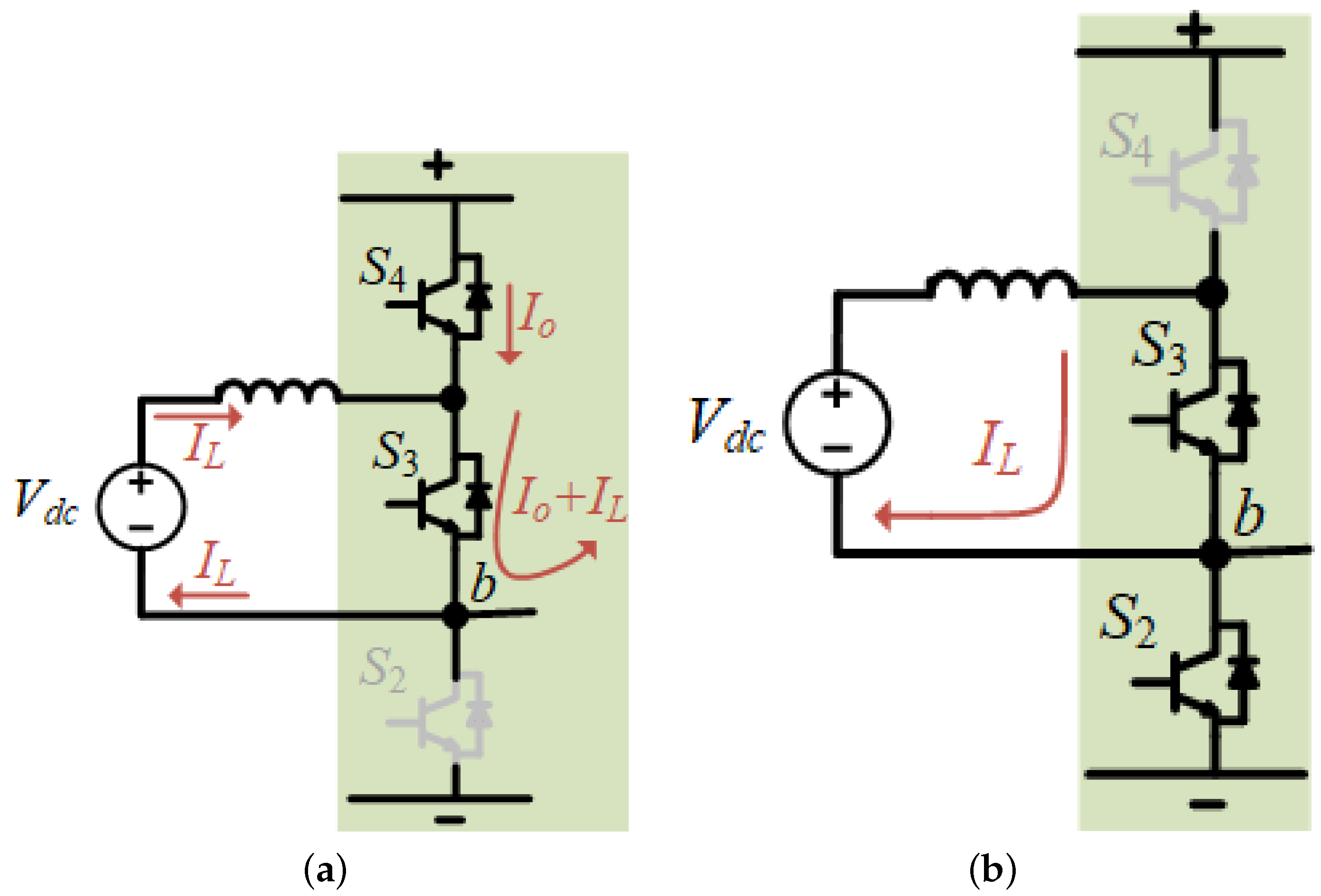
Figure 2 shows the power circuits of the latest developed solution in ref. [32] and the proposed CG topology. The CG boost inverter depicted in Figure 2a is designed to merge the basis of the boost converter with the full bridge inverter. In order to improve the operation of Figure 2a, its boost leg, which consists of three series-connected switches, is analyzed first. One of the three switches must be turned OFF in order to avoid short circuits, as shown in Figure 3. The inductor charging and the load current flow in , thus the current stress of this switch is high. By replacing the boost leg of Figure 2a, a new half-bridges boost inverter is proposed in Figure 2b. The proposed configuration achieves the required switching states as derived in Figure 4. The proposed topology consists of three half-bridges: boost inductor , decoupling capacitor C, and output filter inductor . The following subsection explains the operation of the proposed symmetrical switches-based CG boost inverter.
Figure 2.
The CG boost inverter topology: (a) Conventional topology with asymmetrical stresses, and (b) Proposed topology.
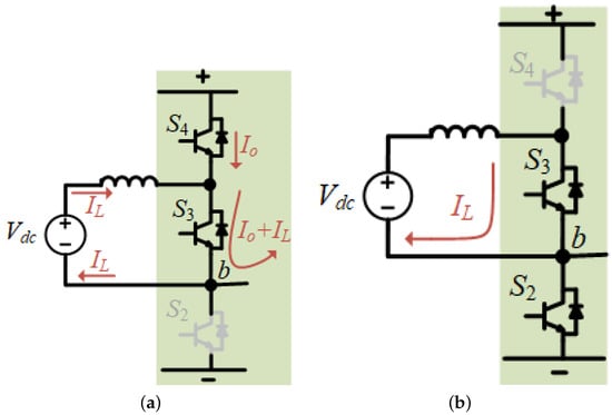
Figure 3.
Switching state during inductor charging for the conventional topology with asymmetrical stresses: (a) First state with the circuit clamped at the upper side, and (b) Second state with the circuit clamped at the lower side.
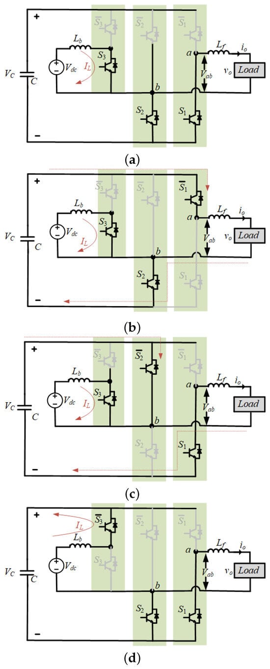
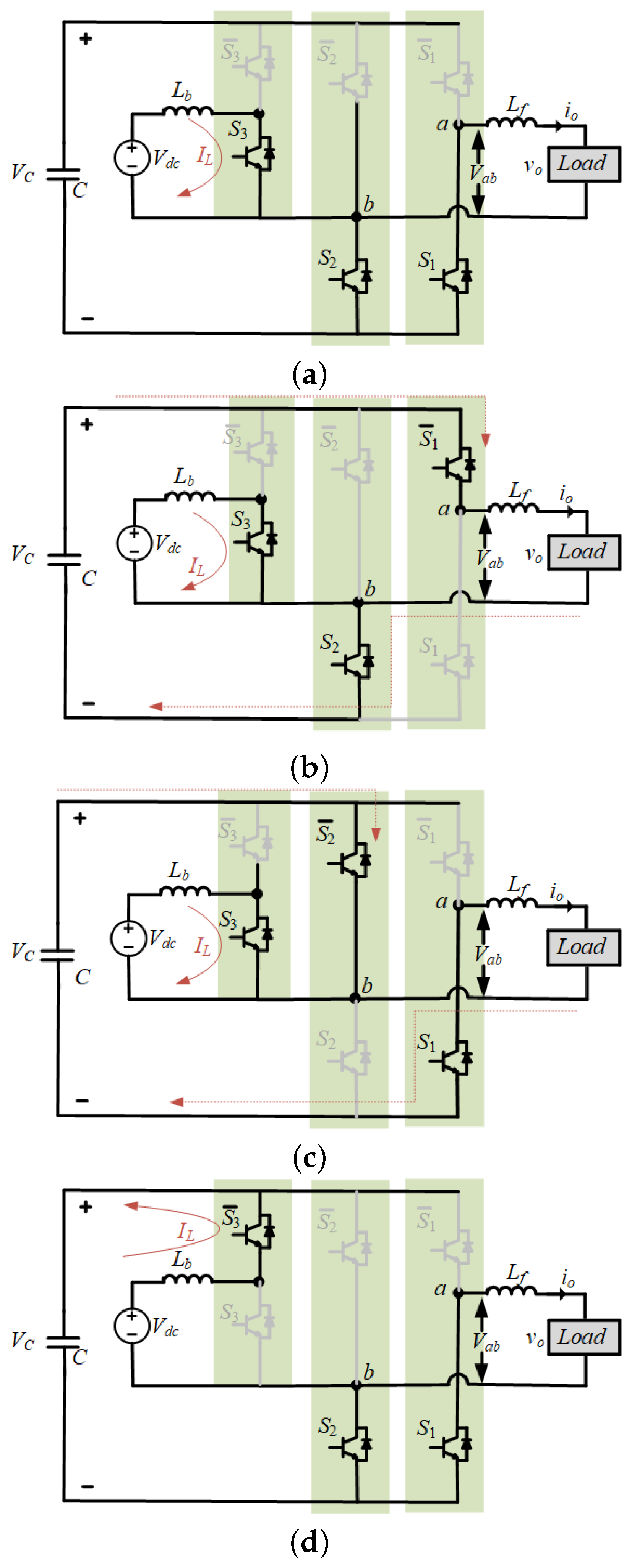
Figure 4.
Switching states for the proposed topology: (a) Inductor charging in the state [0], (b) Inductor charging in the state [+1], (c) Inductor charging in the state [−1] with the inductor current flows through only, and (d) Inductor discharging in the state [0].
2.3. Operation and Switching States
To simplify the operation, Figure 4 shows the switching status of the proposed topology. It is worth noting that the proposed topology simplifies the inverter design by utilizing half-bridge modules and reduces the inverter power losses. During the positive half cycle, the number of switches conducting the load current is reduced. Additionally, diverting the load current away from leads to reducing the current stress on this switch. Therefore, reduced power losses and, hence, a higher lifetime of the switch are achieved using the proposed topology.
The charging and discharging of the inductor are managed by leg c (boost leg) to facilitate the input voltage boosting process. Meanwhile, legs a and b (inverter legs) are responsible for delivering current to the load.
In State 1, the lower switches of legs a and b are turned OFF, resulting in an output inverter voltage of 0 V, as illustrated in Figure 4a. During this state, the inductor is charged through as follows:
In State 2, the lower switch of leg b is turned ON, producing an output inverter voltage = , as shown in Figure 4b. Conversely, in State 3, = when the lower switch of leg a is turned ON as illustrated in Figure 4c. Throughout States 1, 2, and 3, the inductor continues to charge via . It is worth noting that the load current does not pass through during the inductor charging current. Thus, the current stress of this switch is reduced.
When the inductor discharges, the inverter transitions to State 4, where the lower switches of both legs a and b are turned ON, and is turned OFF as shown in Figure 4d. This configuration allows the inductor to release its stored energy into the capacitor network. The voltages across the inductor and capacitors during this discharge phase can be expressed as in (2).
As the boost inductor is charged and discharged with constant duty cycle D, the step-up voltage from the input to the capacitor network is not affected by the sinusoidal modulation. By applying volt-second balance across inductor , the capacitor voltage , similar to the operation of the conventional boost converter, is calculated as:
The constant duty cycle D is given by:
where is a constant reference, and the duty cycle as a function of time is written as:
3. Voltage Gain Calculation and PWM Generation
3.1. Derivation of Voltage Gain
The inverter voltage is related to the capacitor voltage . Therefore, the effective DC gain is computed as in (7).
Which can be rearranged as follows:
The fundamental peak output voltage of the proposed is calculated as:
where M = / is the modulation index. The duty cycle generated by the sinusoidal reference can be written as a function of time as follows:
The overall gain of the proposed boost inverter can be computed in (10). In order to avoid operation in the over modulation region, which leads to elevated THD, the maximum allowable modulation index is constrained by D.
3.2. Modulation Strategy
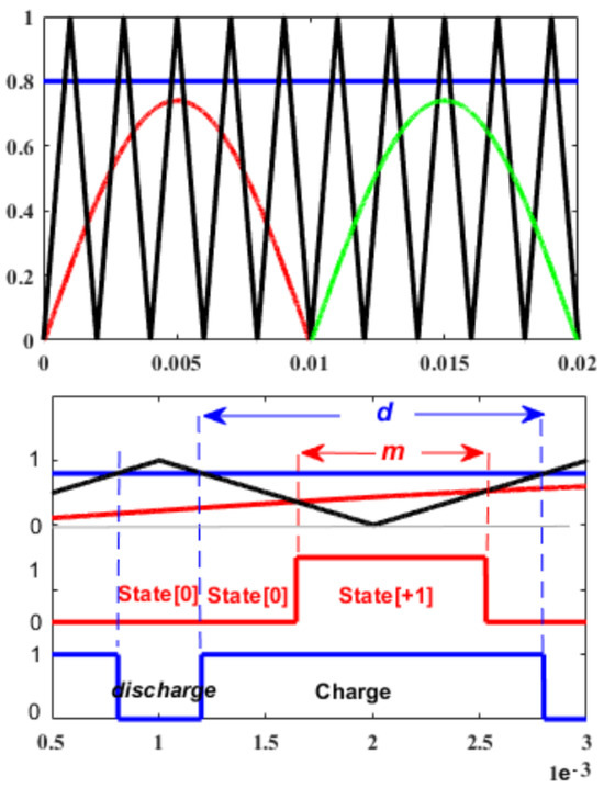
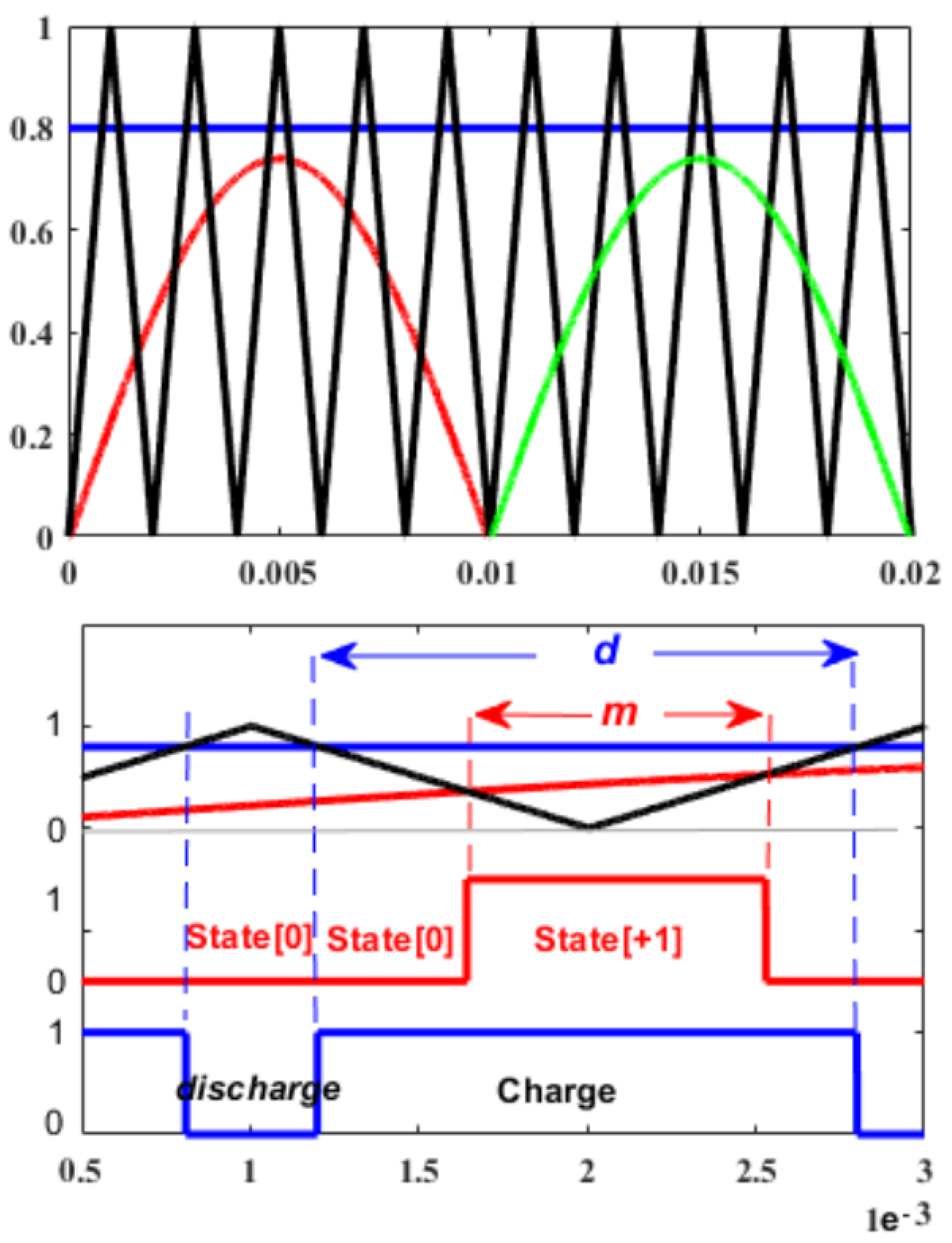
The sinusoidal modulation with constant PWM offers a simplified approach by separates the control of the boost and inverter operation, where the duty cycle directly regulates the DC voltage gain and manage the charging and discharging of the inductor . The sinusoidal modulation shapes the AC output. This structure simplifies the control design by reducing coupling and avoids the need for complex multi-loop coordination, where the DC–DC voltage boosting is independent of the sinusoidal modulation used to control the AC output. This decoupling significantly streamlines circuit analysis, allowing the standard equations of a conventional boost converter to be directly applied. Figure 5 illustrates the key waveforms of the modulation and the switching status summarized in Table 1. In the meantime, one leg (a or b) operates at a line frequency, resulting in lower losses. The switch state in each half cycle is summarized in Table 2.
Figure 5.
Key waveforms of sinusoidal modulation with constant PWM.
Table 1.
Switching states of the proposed topology.
Table 2.
Switch states in each half cycle.
3.3. Current and Voltage Stresses of Switches
The peak current and voltage for each device of the proposed topology are summarized in Table 3. It is worth highlighting that the proposed not only achieves the boosting with CG configuration by using three half-bridges but also reduces the current stress of the boost switch by one power switch in comparison to the common ground boost inverter presented in [32].
Table 3.
Comparison of device stress and overall total stress between conventional and proposed boost inverter topologies.
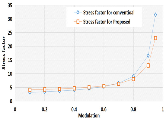
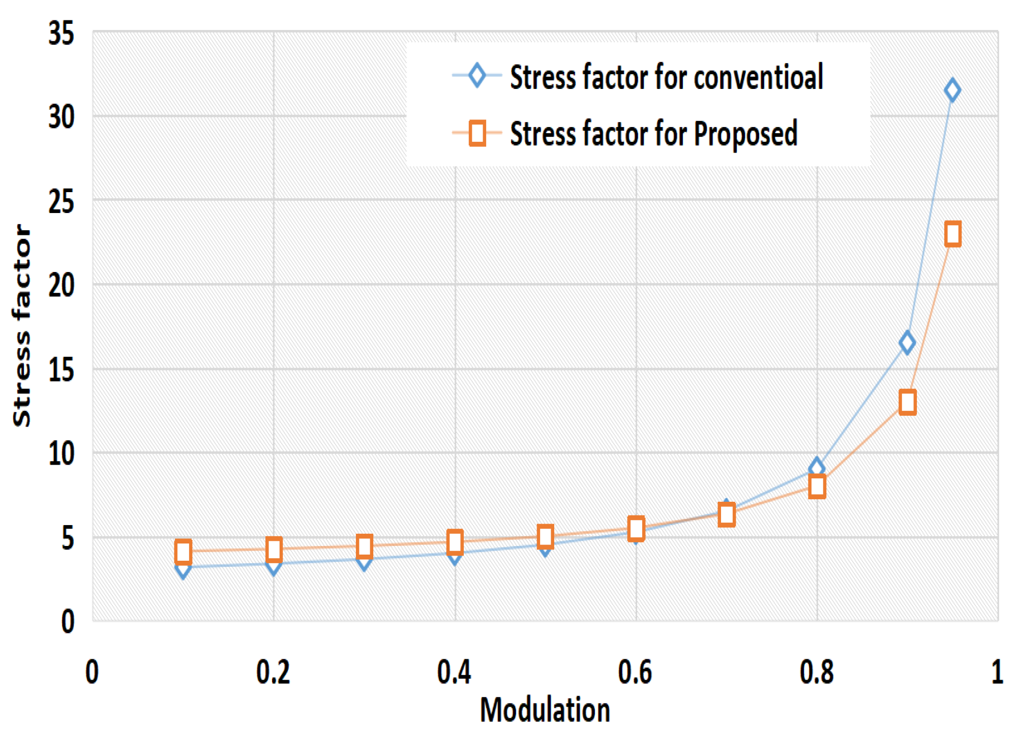
Using power balance and the voltage gain , the maximum dc input current is given by . For example, at m = D = 0.8, the overall stress for the conventional topology is 9, while the stress for the proposed is 8. Figure 6 shows a comparison of the total stress factor at different modulations.
Figure 6.
Comparison of the total stress factor.
4. Simulation and Experimental Results
4.1. Simulation Results
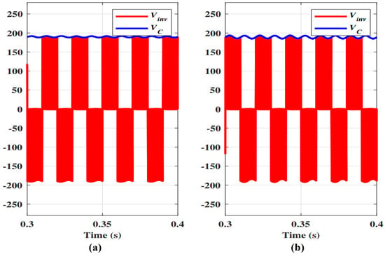
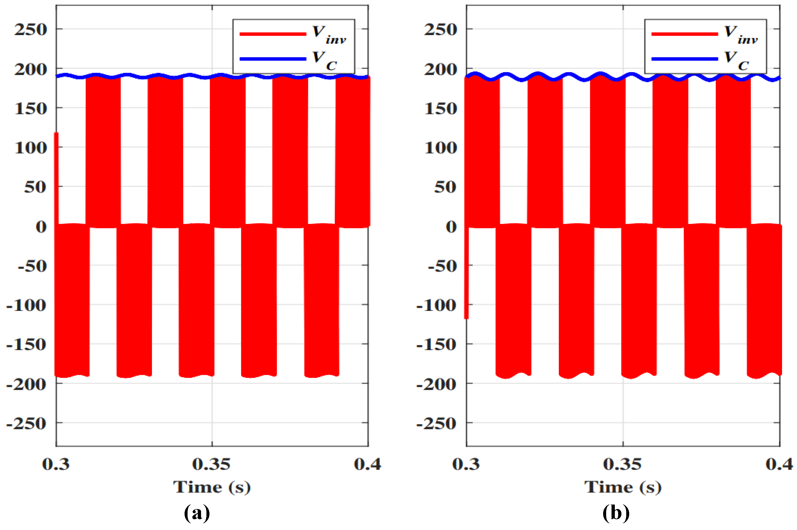
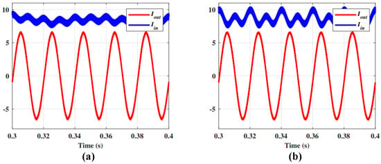
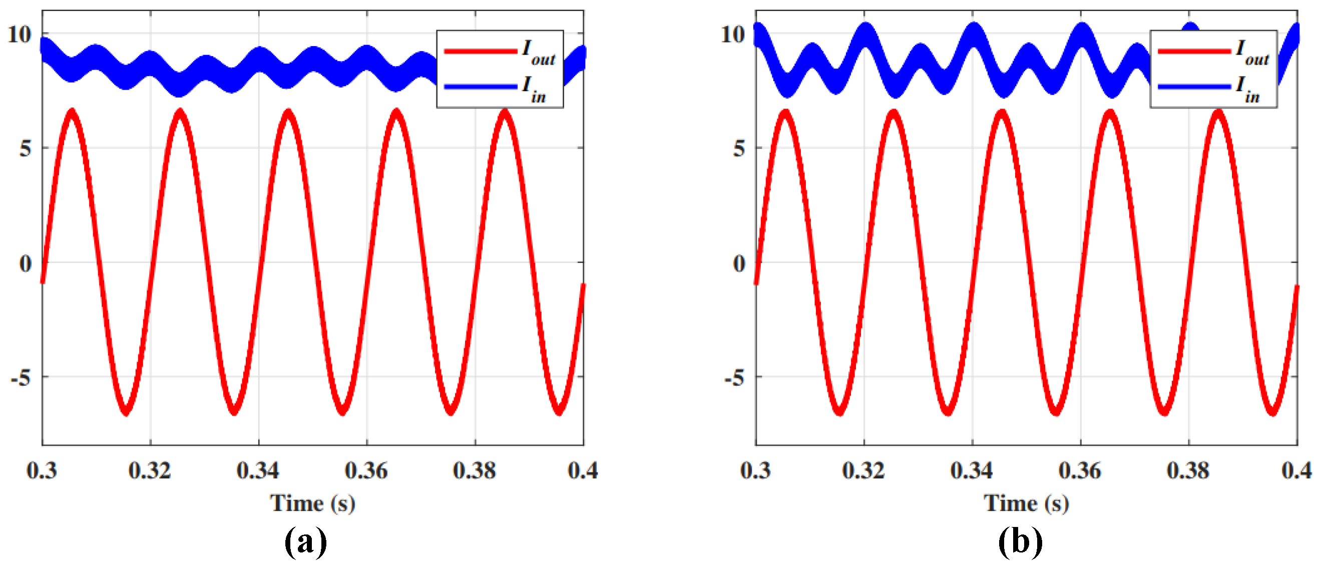
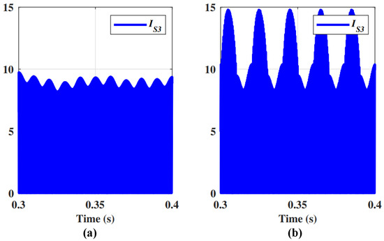
A case study was conducted using MATLAB/SIMULINK 2024b to evaluate the proposed system. For a fair comparison, the same parameters are used for both the topology of the latest topology presented in [32] and the proposed topology. The simulation parameters included an input DC voltage of 50 V, an output filter inductance of 10 mH, a switching frequency of 20 kHz, and a boost inductor of 2 mH. The duty cycle of both simulations was set to 0.75 to produce 200 V across the capacitor, as shown in Figure 7. The simulation results, presented in Figure 8, show the inductor current and the output current for both topologies. The better inductor current is achieved in the case of the proposed topology. The boost switch current illustrated in Figure 9 demonstrates that the proposed topology effectively reduces the current stress on switch compared to [32].
Figure 7.
Comparison of the capacitor and the inverter voltage for: (a) The proposed topology, and (b) The conventional topology with asymmetrical stresses.
Figure 8.
Comparison of the input and the output current for: (a) The proposed topology, and (b) The conventional topology with asymmetrical stresses.
Figure 9.
Comparison of the boost switch S3 for (a) The proposed topology, and (b) The conventional topology with asymmetrical stresses.
4.2. Experimental Results
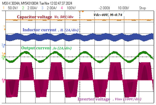
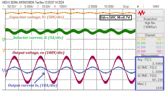
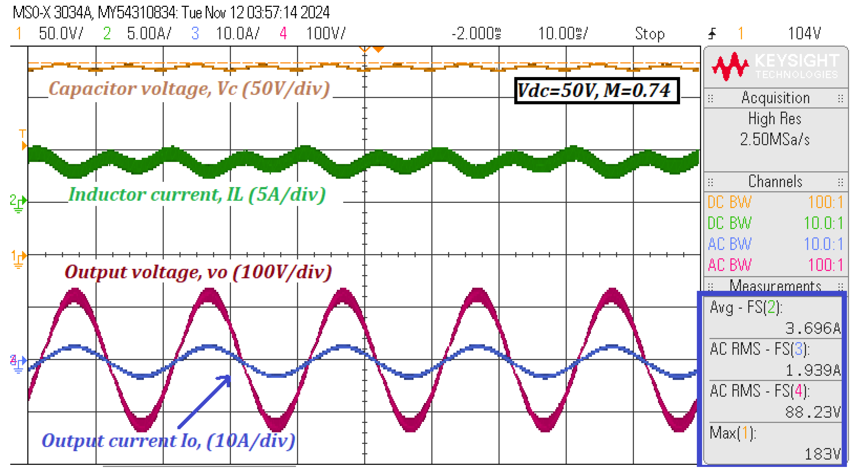
In order to verify the proposed topology, an experimental prototype was designed using three half-bridges and tested in the lab. A Texas Instruments DSP (TMS320F28035) was employed to generate the sinusoidal PWM scheme. The system specifications are listed in Table 4. The experimental evaluation was conducted by varying the modulation index and duty cycle to examine the operating characteristics and voltage gain capability of the proposed converter, while maintaining identical hardware configuration, switching frequency, and ambient conditions to ensure measurement consistency. Figure 10 shows the measured average capacitor voltage of 147 V when the input voltage is set to 40 V, which is approximately 6 V lower than the analytical value, with modulation index m = 0.74 and the duty cycle D = 0.74. The corresponding average inductor current and load current are 1.25 A and 0.58 A rms, respectively, indicating continuous inductor current operation with a relatively constant current ripple. Figure 11 illustrates the performance at higher power with an input voltage of 50 V, where the average inductor current reaches 3.7 A and the load current is 1.95 A rms. Hence, the acquired input power and output power are approximately 185 W and 171 W, resulting in an efficiency of approximately 92%.
Table 4.
Experimental specifications.
Figure 10.
Experimental results at = 40 V, and = 50 W.
Figure 11.
Experimental results at = 50 V, and = 185 W.
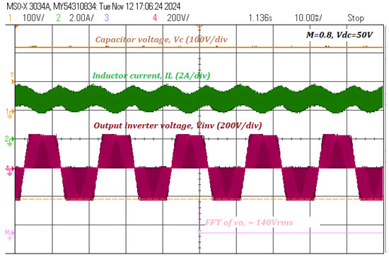
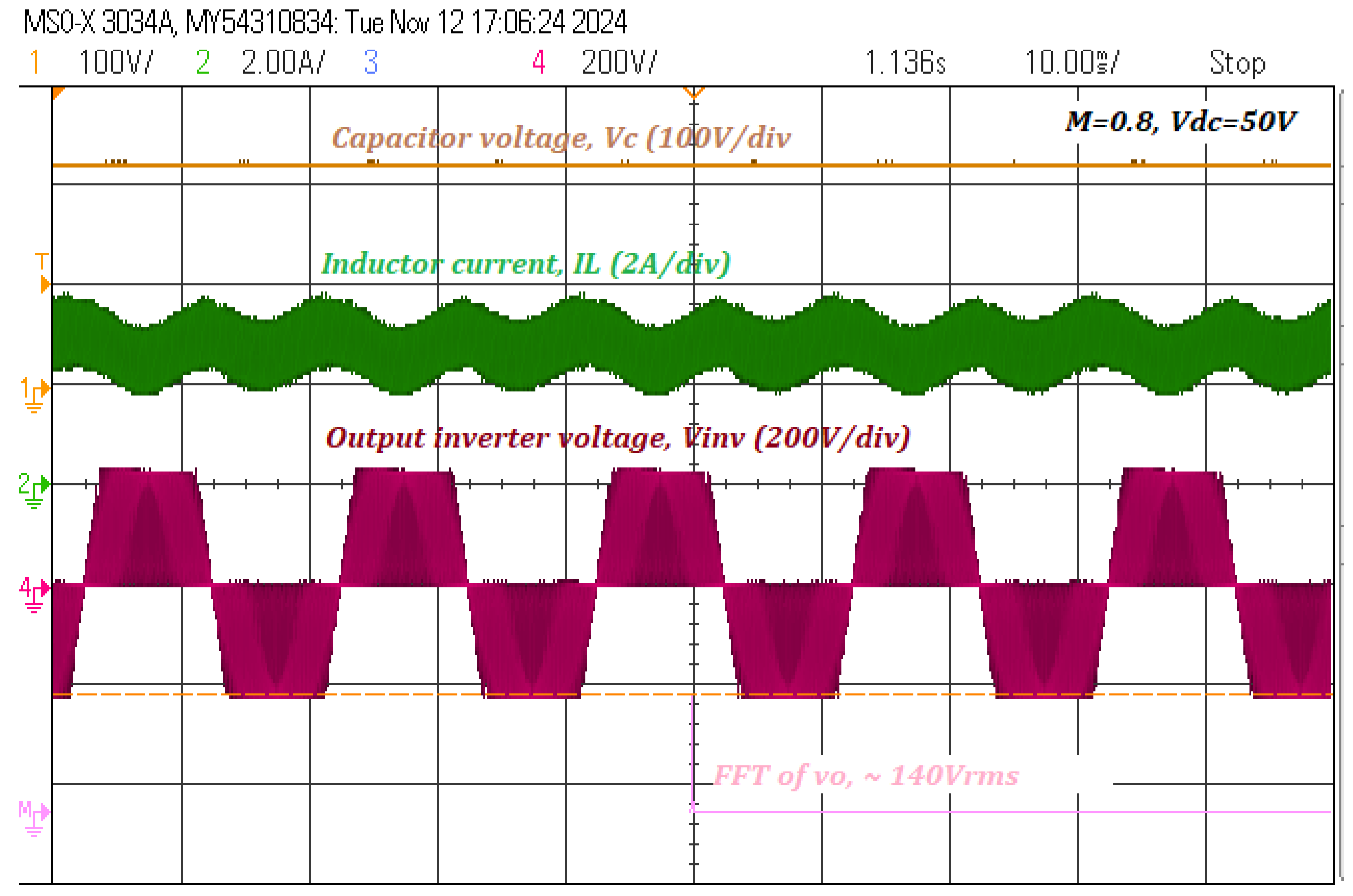
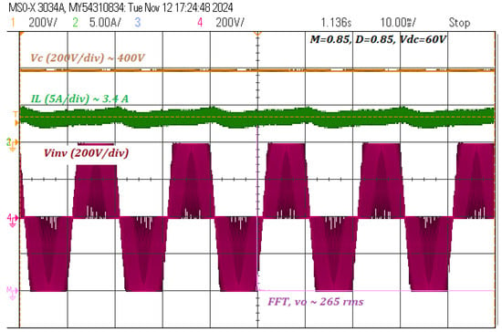
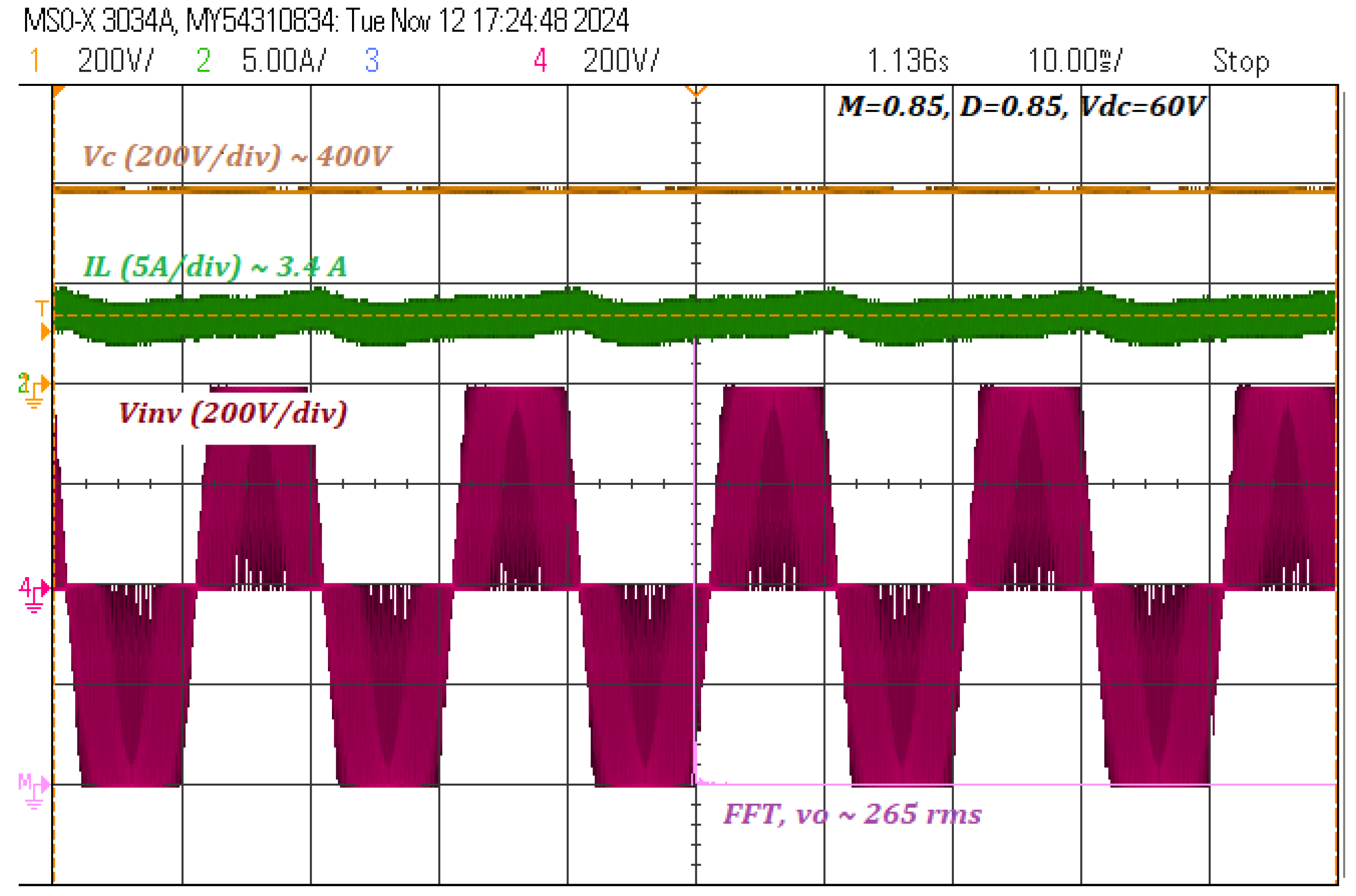
Further tests were performed by increasing the duty cycle D to 0.8 and 0.85, leading to capacitor voltages of 225 V and 400 V, as shown in Figure 12 and Figure 13, respectively, confirming the high voltage gain capability of the proposed topology.
Figure 12.
Experimental results at = 50 V, and = 145 W.
Figure 13.
Experimental results at = 60 V, and = 200 W.
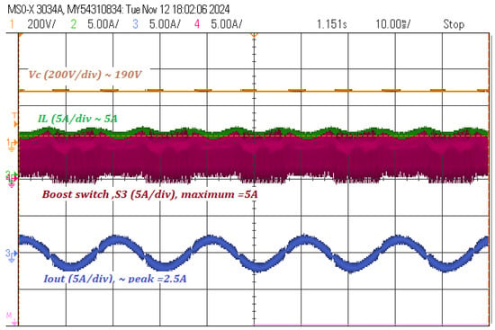
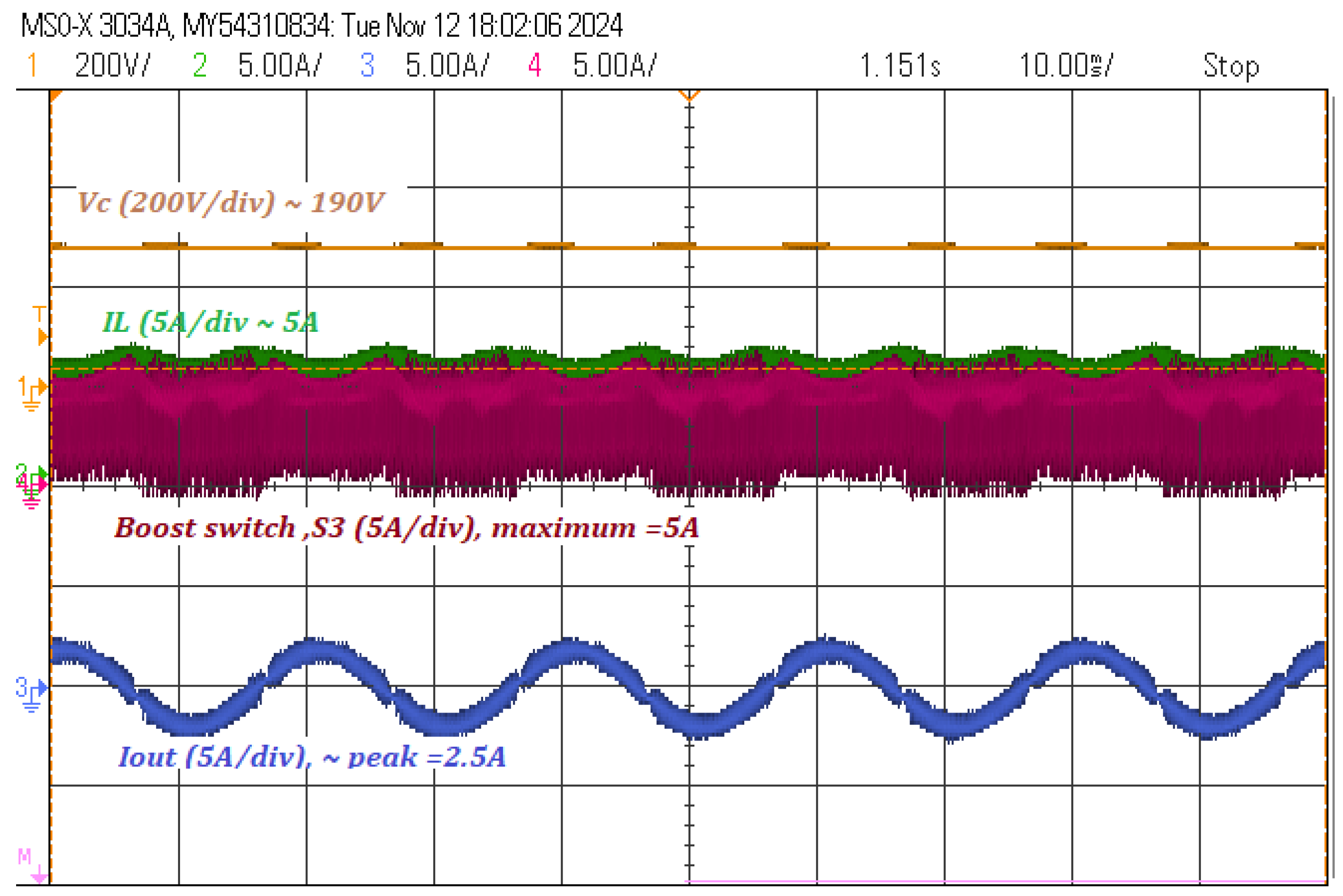
The current stress of the boost switch was experimentally measured and is illustrated in Figure 14. The results show that the maximum current stress is approximately 5 A, which corresponds to the inductor current, while the peak output current is about 2.5 A. This confirms that the output current is diverted away from the boost switch, validating the reduced device stress characteristic of the proposed topology.
Figure 14.
The current stress through the boost switch , and the inductor current.
5. Performance Comparison
Table 5 provides a comparative analysis of recent common-ground boost inverters with similar functionality, focusing on their ability to achieve voltage boosting while maintaining a common ground configuration. The proposed inverter incorporates an additional switch, which plays a crucial role in minimizing current stress compared to [26,28,32]. The topologies in [33,34,35,37,38,39,41] provide zero leakage current; however, they suffer from discontinuous inductor current and asymmetrical required semiconductor switches. The proposed topology preserves continuous inductor current and uses symmetrical switches. Furthermore, the proposed topology does not require diodes, compared to the topologies in [33,34,35,37,39,42].
Table 5.
Comparison of proposed topology with featured existing topologies in the literature.
6. Closed-Loop Performance
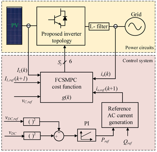
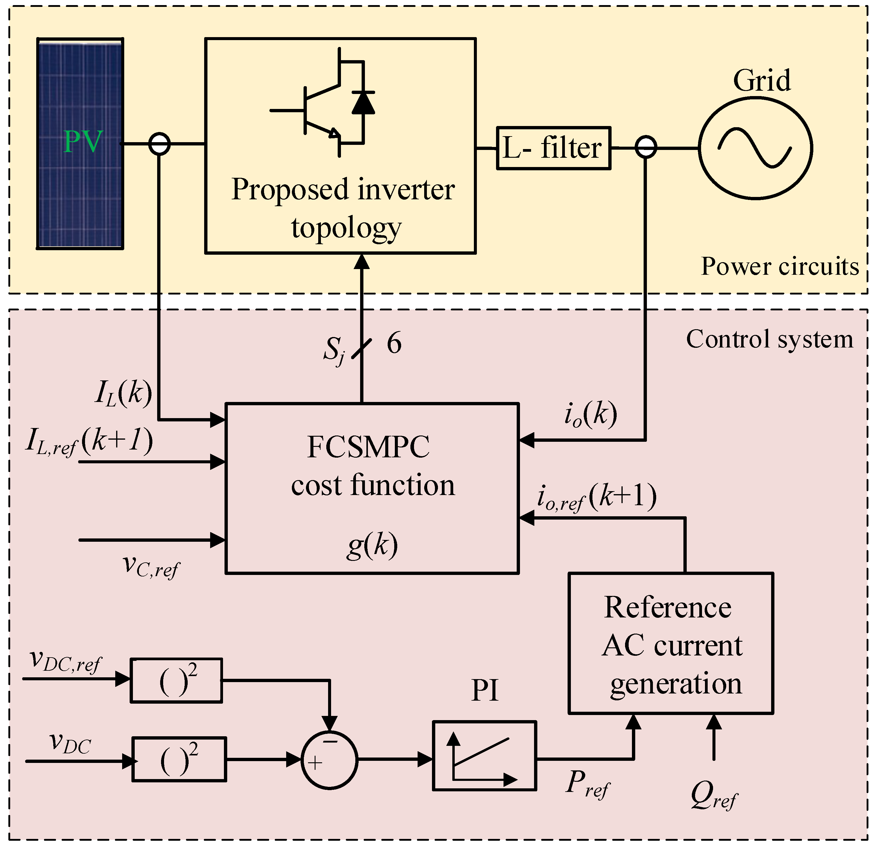
To validate the dynamic performance of the proposed topology in grid-connected mode, a simulation case study with a finite control set model predictive controller (FCSMPC) has been designed. The complete closed-loop controller stages are shown in Figure 15. The control stage has to regulate the DC-link voltage at its reference ( = ), which is made by a separate PI controller. The closed loop has to control DC-input current at its reference, which is determined mainly by the MPPT algorithm ( = ). In addition, control of the injected AC-side grid current is essential to generate sinusoidal grid-following current based on active and reactive powers ( = ). The control of and is made using FCSMPC control, based on the presented basis in [42]. Closed-loop case study parameters are shown in Table 6.
Figure 15.
Closed-loop control stages using cascaded PI and FCSMPC method.
Table 6.
Closed-loop case study parameters.
The considered scenarios are:
- 1.
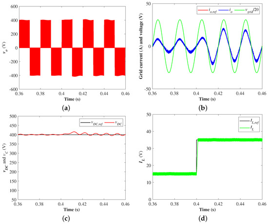
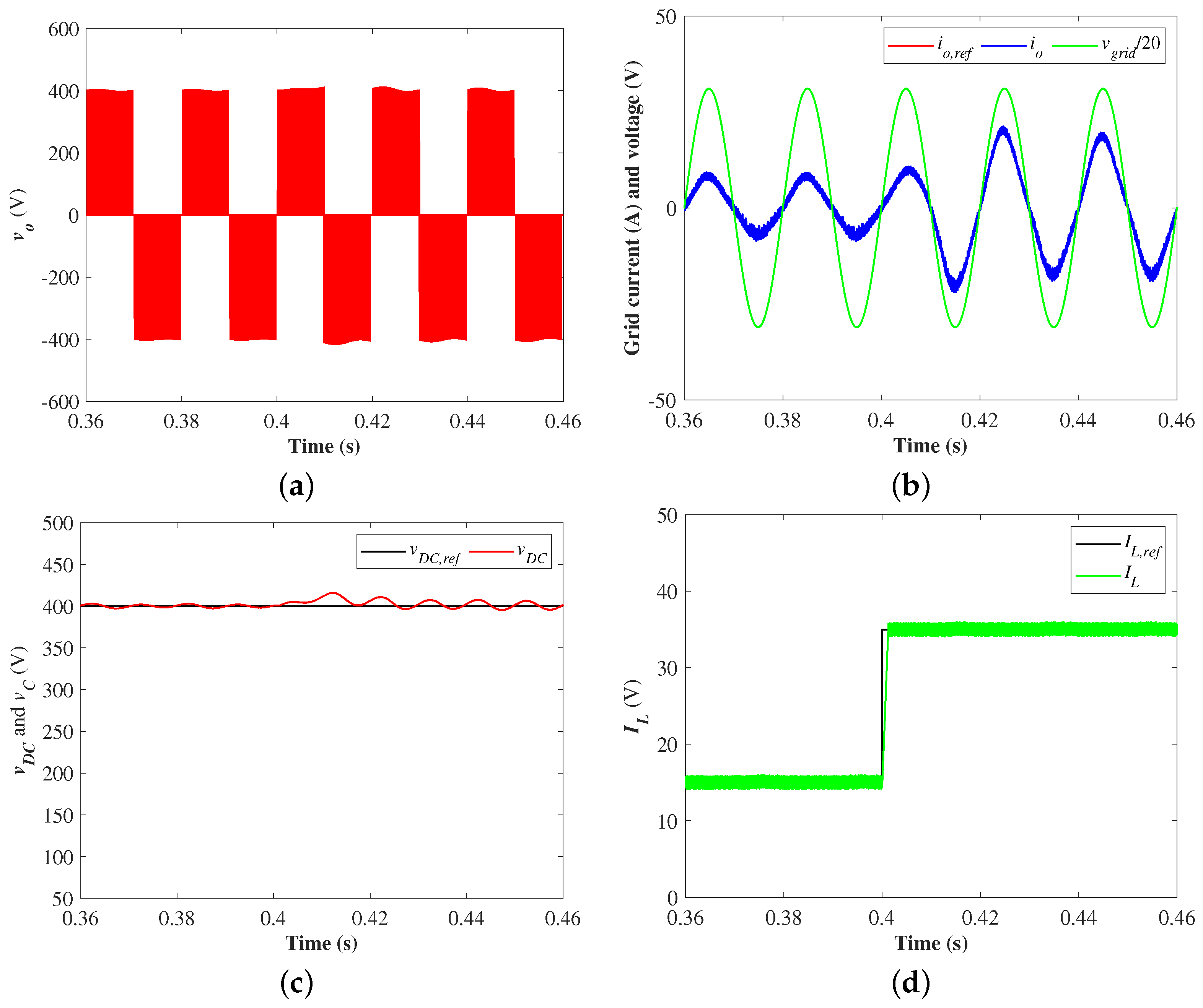
- Case 1: step change in reference input power with a change in the inductor current reference from 15 A to 35 A. The results of this case are shown in Figure 16.Figure 16. Performance of the closed-loop FCSMPC controller with the proposed topology at step change in inductor current from 15 A to 35 A reference. (a) Inverter voltage. (b) Grid current and scaled voltage. (c) DC-link regulation. (d) Inductor input current control.
- 2.
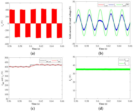
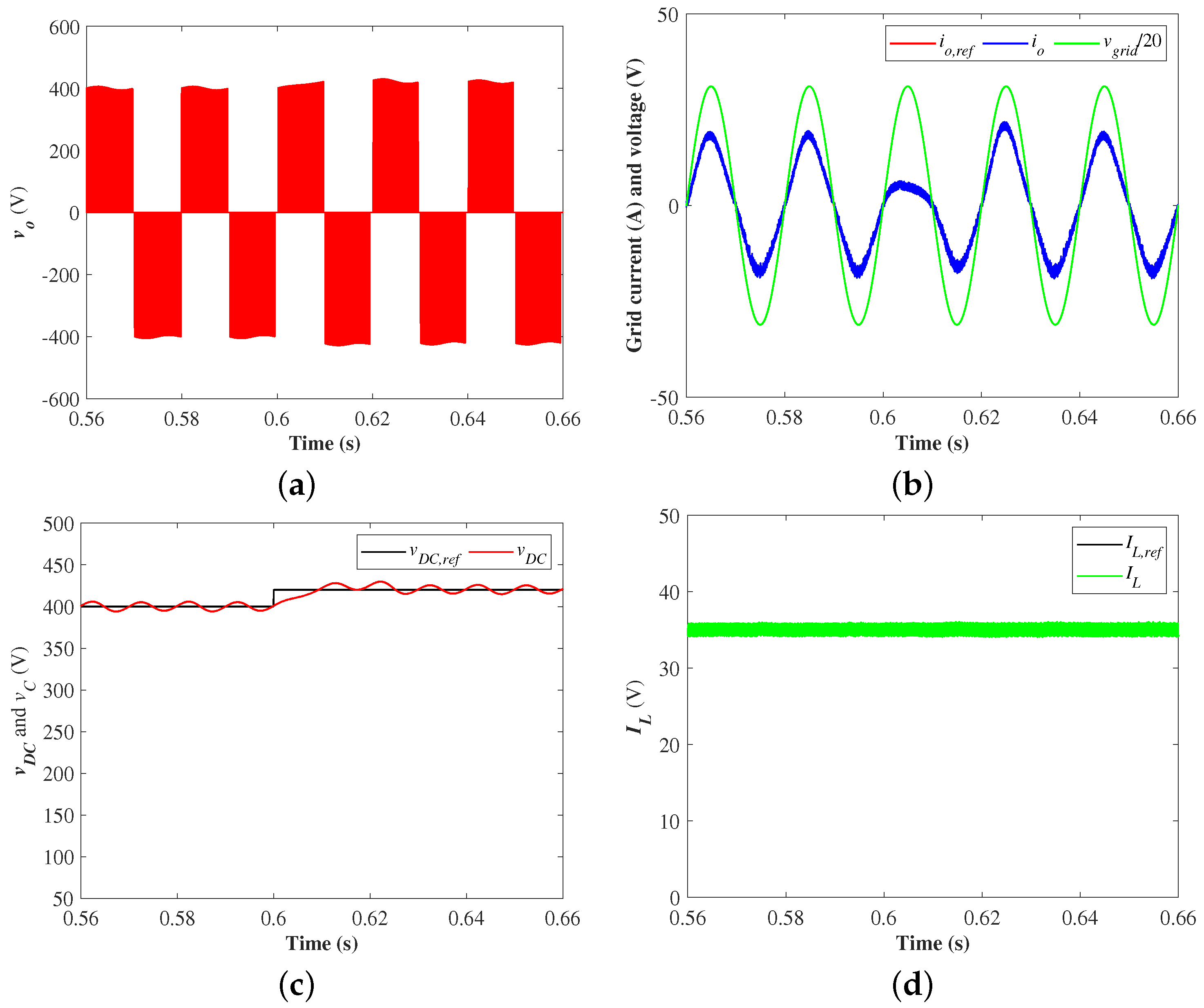
- Case 2: step change in DC-link reference voltage with a change in the reference from 400 V to 420 V, as shown in Figure 17.Figure 17. Performance of the closed-loop FCSMPC controller with the proposed topology at step change in dc-link reference from 400 V to 420 V. (a) Inverter voltage. (b) Grid current and scaled voltage. (c) DC-link regulation. (d) Inductor input current control.
- 3.
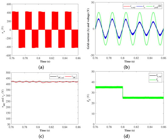
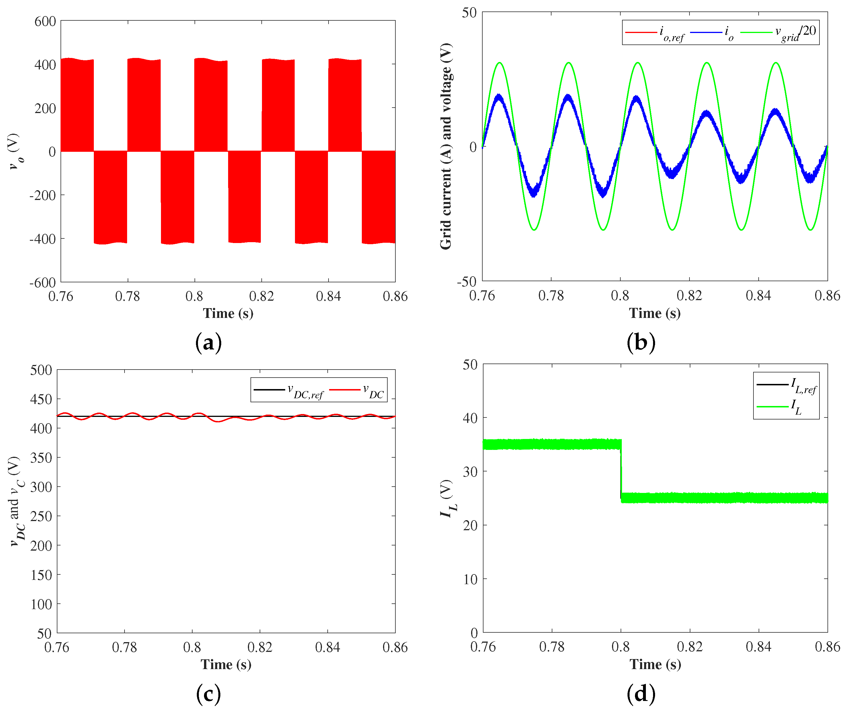
- Case 3: step down in reference input inductor current reference from 35 A to 25 A. The results of this case are shown in Figure 18.Figure 18. Performance of the closed-loop FCSMPC controller with the proposed topology at step change in inductor current from 35 A to 25 A reference. (a) Inverter voltage. (b) Grid current and scaled voltage. (c) DC-link regulation. (d) Inductor input current control.
- 4.
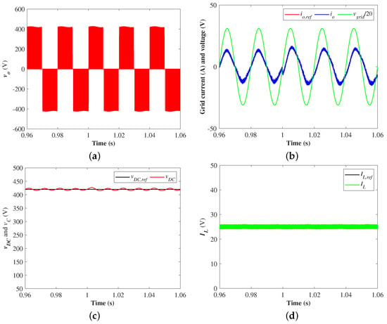
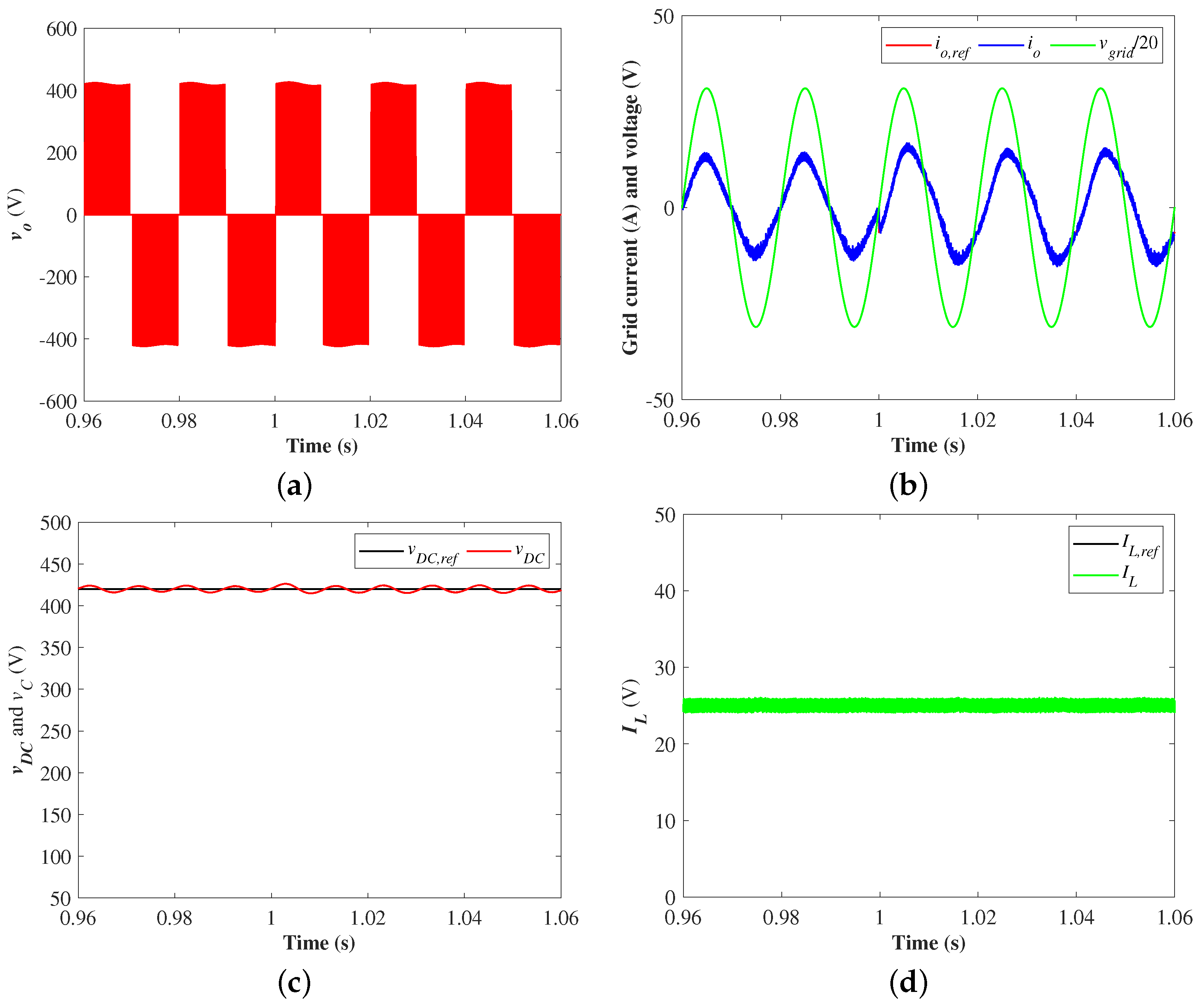
- Case 4: step in reactive power injection reference from 0 VAR to 1000 VAR. The results of this case are shown in Figure 19.Figure 19. Performance of the closed-loop FCSMPC controller with the proposed topology at reactive power injection from 0 to 1000 VAR. (a) Inverter voltage. (b) Grid current and scaled voltage. (c) DC-link regulation. (d) Inductor input current control.
6.1. Case 1: Input Power Increased
The results of this scenario are shown in Figure 16. The inverter output voltage is shown in Figure 16a. It can be seen that the injected AC current in Figure 16b is sinusoidal and follows the grid side voltage, even if there is a step increase in the input power from the DC source. In addition, the regulated DC-link voltage follows the reference 400 V signal in both cases, as shown in Figure 16c. The input inductor current in Figure 16d tracks the reference current change from 15 A to 35 A quickly and accurately, owing to the FCSMPC method. The results demonstrate the dynamic performance of the topology in response to a step-change increase in input power from PV panels.
6.2. Case 2: Change of DC-Link Reference Voltage
In this scenario, the reference signal for DC-link regulation is changed from 400 V to 420 V. Because there are no changes in input power or reactive power, the DC and AC currents remain constant in this scenario. DC-link regulation is achieved quickly, with minimal peak overshoot, due to the PI control design, as shown in Figure 17c. In addition, there are no fluctuations or transients in the DC and AC currents in this scenario, as shown in Figure 17b and Figure 16d, respectively.
6.3. Case 3: Input Power Decreased
The corresponding results for this scenario are shown in Figure 18. The reference input current is decreased from 35 A to 25 A as shown in Figure 18d. The FCSMPC achieves fast response and accurate tracking in both cases with high performance during the step change. In addition, the regulation of AC current and DC-link voltage are preserved at their references as shown in Figure 18b and Figure 18c, respectively.
6.4. Case 4: Reactive Power Injection to the Grid
In this scenario, the dynamic performance of the proposed topology and the designed controllers is tested under a reactive power injection of 1000 VAR. The inverter output voltage is shown in Figure 19a. It can be seen that the AC current has a phase shift from the grid voltage and tracks the reference current signal, as shown in Figure 19b. Furthermore, the DC-link voltage regulation is free from fluctuations and transients in this scenario, as shown in Figure 19c. As there is no change in the input-side active power, Figure 19d shows a constant, transactions-free DC-side current tracking.
7. Conclusions
Modern boost inverters extensively employ half-bridge configurations due to their modularity and suitability for high-power-density applications. This paper presented a symmetrical switching topology derived from the common-ground boost inverter using a half-bridge structure. The proposed converter provides voltage boosting while preserving a common-ground configuration, as confirmed through analytical derivation of the operating principle, voltage gain, and modulation limits. Compared with conventional common-ground boost inverters, the proposed topology reduces the peak current stress on the main boost switch from + to resulting in a lower overall device stress and improved reliability. These advantages are verified by steady-state and switching waveforms obtained from both simulation and experimental results, which closely match the theoretical analysis. The simple complementary gating scheme further supports practical implementation and integration with renewable energy systems. Overall, the analytical, simulation, and experimental results demonstrate the effectiveness and practical applicability of the proposed topology. Future research includes developing an industrial version of the proposed topology, measuring power density and loss breakdown, and studying its efficiency across various operating conditions.
Author Contributions
Conceptualization, E.A.D.I., M.A. and M.O.; methodology, E.A.D.I., M.A. and M.O.; software, E.A.D.I., M.A. and M.O.; validation, E.A.D.I., M.A. and M.O.; formal analysis, E.A.D.I., M.A. and M.O.; investigation, E.A.D.I., M.A. and M.O.; resources, E.A.D.I., M.A. and M.O.; data curation, E.A.D.I., M.A. and M.O.; writing—original draft preparation, E.A.D.I., M.A. and M.O.; writing—review and editing, E.A.D.I., M.A. and M.O.; visualization, E.A.D.I., M.A. and M.O.; supervision, E.A.D.I., M.A. and M.O.; project administration, E.A.D.I., M.A. and M.O.; funding acquisition, E.A.D.I., M.A. and M.O. All authors have read and agreed to the published version of the manuscript.
Funding
This work was supported by ANID FONDECYT Iniciación 11230430.
Institutional Review Board Statement
No applicable.
Informed Consent Statement
No applicable.
Data Availability Statement
The original contributions presented in this study are included in the article. Further inquiries can be directed to the corresponding author.
Conflicts of Interest
The authors declare no conflicts of interest.
References
- Drăcea, R.M.; Cristea, M.; Sitnikov, C.; Nimerenco, I.; Nedelcu, A. Regional Energy Transition: Decoupling CO2 Emissions and Policy Perspectives. Sustainability 2026, 18, 652. [Google Scholar] [CrossRef] [Scilit]
- Manimala, P.; Balaraman, S. A hybrid technique for grid-tied photovoltaic (PV) systems utilizing a modular multilevel inverter (MMI) topology. Energy 2025, 324, 135826. [Google Scholar] [CrossRef] [Scilit]
- International Renewable Energy Agency (IRENA). Global Renewable Energy Statistics. In IRENA Publications; International Renewable Energy Agency (IRENA): Abu Dhabi, United Arab Emirates, 2023. [Google Scholar]
- Coelho, S.; Monteiro, V.; Afonso, J.L. Topological Advances in Isolated DC–DC Converters: High-Efficiency Design for Renewable Energy Integration. Sustainability 2025, 17, 2336. [Google Scholar] [CrossRef] [Scilit]
- Zhang, L.; Sun, K.; Li, Y.W.; Lu, X.; Zhao, J.; Zhao, Y.; Gao, S.; Wang, H. A Distributed Power Control of Series-Connected Module-Integrated Inverters for PV Grid-Tied Applications. IEEE Trans. Power Electron. 2018, 33, 7698–7707. [Google Scholar] [CrossRef] [Scilit]
- Santhi, R.; Srinivasan, A. An efficient AOA-RERNN control approach for a non-isolated quasi-Z-source novel multilevel inverter based grid connected PV system. Energy 2023, 263, 125492. [Google Scholar] [CrossRef] [Scilit]
- Venkata Pavan Kumar, Y.; Naga Venkata Bramareswara Rao, S.; Pradeep, D.J. Fuzzy-Based Current-Controlled Voltage Source Inverter for Improved Power Quality in Photovoltaic and Fuel Cell Integrated Sustainable Hybrid Microgrids. Sustainability 2025, 17, 4520. [Google Scholar] [CrossRef] [Scilit]
- Rahman, K.; Hashimoto, J.; Koseki, K.; Ustun, T.S.; Orihara, D.; Kikusato, H. Synergistic Control of Active Filter and Grid Forming Inverter for Power Quality Improvement. Sustainability 2024, 16, 9068. [Google Scholar] [CrossRef] [Scilit]
- Trabelsi, M.; Vahedi, H.; Abu-Rub, H. Review on Single-DC-Source Multilevel Inverters: Topologies, Challenges, Industrial Applications, and Recommendations. IEEE Open J. Ind. Electron. Soc. 2021, 2, 112–127. [Google Scholar] [CrossRef] [Scilit]
- Qureshi, M.A.; Torelli, F.; Stella, F.; Musumeci, S.; Mazza, A.; Chicco, G. A Novel Model Reference Adaptive Control Approach for Three-Phase Inverter Applications. IEEE J. Emerg. Sel. Top. Power Electron. 2025, 14, 467–478. [Google Scholar] [CrossRef] [Scilit]
- Liu, Z.; Cheng, X.; Peng, X.; Wang, P.; Zhao, X.; Liu, J.; Jiang, D.; Qu, R. A review of common-mode voltage suppression methods in wind power generation. Renew. Sustain. Energy Rev. 2024, 203, 114773. [Google Scholar] [CrossRef] [Scilit]
- Ye, Y.; Deng, W.; Ye, Z.; Belhora, F.; Zhang, J.W. Smart monitoring of potential induced leakage current of photovoltaic under salt mist environment based on passive optical Fabry–Perot interference sensor. Sol. Energy 2025, 299, 113695. [Google Scholar] [CrossRef] [Scilit]
- Wu, Y.K.; Lin, J.H.; Lin, H.J. Standards and Guidelines for Grid-Connected Photovoltaic Generation Systems: A Review and Comparison. IEEE Trans. Ind. App. 2017, 53, 3205–3216. [Google Scholar] [CrossRef] [Scilit]
- Li, W.; Gu, Y.; Luo, H.; Cui, W.; He, X.; Xia, C. Topology Review and Derivation Methodology of Single-Phase Transformerless Photovoltaic Inverters for Leakage Current Suppression. IEEE Trans. Ind. Electron. 2015, 62, 4537–4551. [Google Scholar] [CrossRef] [Scilit]
- Yu, T.; Wan, W.; Duan, S. A Modulation Method to Eliminate Leakage Current and Balance Neutral-Point Voltage for Three-Level Inverters in Photovoltaic Systems. IEEE Trans. Ind. Electron. 2023, 45, 1635–1645. [Google Scholar] [CrossRef] [Scilit]
- Palanisamy, R. Mitigation of capacitor voltage unbalance and common mode voltage for 3-phase 5-Level NPC inverter using hexagonal SVPWM. e-Prime Adv. Electr. Eng. Electron. Energy 2024, 9, 100639. [Google Scholar] [CrossRef] [Scilit]
- Vazquez-Guzman, G.; Martinez-Rodriguez, P.R.; Rosas-Caro, J.C.; Rivera-Perez, E.; Verdin-Cruz, J.A.; Rodriguez-Cortes, C.J.; Langarica-Cordoba, D. Three-Phase Space Vector PWM Inverter for Induction Motor Drive with Leakage Current Reduction. Sustainability 2025, 17, 9317. [Google Scholar] [CrossRef] [Scilit]
- Ma, Z.; Niu, H.; Wu, X.; Zhang, X.; Lin, G. An Improved Overmodulation Strategy for a Three-Level NPC Inverter Considering Neutral-Point Voltage Balance and Common-Mode Voltage Suppression. Sustainability 2022, 14, 12558. [Google Scholar] [CrossRef] [Scilit]
- Barbie, E.; Kuperman, A.; Baimel, D. Analytical line-voltage THD formulation and optimization for sine- and third harmonic injection PWM in three-phase cascaded H-bridge multilevel inverters with fixed and variable DC supply ratios. Energy 2025, 318, 134669. [Google Scholar] [CrossRef] [Scilit]
- Kerekes, T.; Teodorescu, R.; Rodríguez, P.; Vázquez, G.; Aldabas, E. A New High-Efficiency Single-Phase Transformerless PV Inverter Topology. IEEE Trans. Ind. Electron. 2011, 58, 184–191. [Google Scholar] [CrossRef] [Scilit]
- Wang, H.; Wu, W.; Yuan, L.; Orabi, M.; Koutroulis, E.; Chung, H.S.H.; Liserre, M.; Blaabjerg, F. Topology Review of Transformer-Less Single-Phase Common-Ground Converters: Inverters. IEEE J. Emerg. Sel. Top. Power Electron. 2025, 13, 4798–4841. [Google Scholar] [CrossRef] [Scilit]
- Guo, X.; Zhang, H.; Tang, W.; Lu, Z.; Hua, C.; Siwakoti, Y.P.; Malinowski, M.; Blaabjerg, F. Overview of Recent Advanced Topologies for Transformerless Dual-Grounded Inverters. IEEE Trans. Power Electron. 2022, 37, 12679–12704. [Google Scholar] [CrossRef] [Scilit]
- Lee, S.S.; Ho, A.V.; Barzegarkhoo, R.; Grigoletto, F.B.; Siwakoti, Y.P.; Cao, S. Single-Phase Boost Inverters Designed Using Half-Bridges. IEEE Trans. Ind. Electron. 2024, 71, 11690–11695. [Google Scholar] [CrossRef] [Scilit]
- Gaafar, M.A.; Orabi, M.; Ibrahim, A.; Kennel, R.; Abdelrahem, M. Common-Ground Photovoltaic Inverters for Leakage Current Mitigation: Comparative Review. Appl. Sci. 2021, 11, 11266. [Google Scholar] [CrossRef] [Scilit]
- Yao, Z.; Xu, Q. Topology Derivation Method of Common-Ground Transformerless Single-Phase Inverters Based on Graph Theory. IEEE Trans. Power Electron. 2025, 40, 4510–4521. [Google Scholar] [CrossRef] [Scilit]
- Gu, Y.; Li, W.; Zhao, Y.; Yang, B.; Li, C.; He, X. Transformerless Inverter With Virtual DC Bus Concept for Cost-Effective Grid-Connected PV Power Systems. IEEE Trans. Power Electron. 2013, 28, 793–805. [Google Scholar] [CrossRef] [Scilit]
- Grigoletto, F.B. Multilevel Common-Ground Transformerless Inverter for Photovoltaic Applications. IEEE J. Emerg. Sel. Top. Power Electron. 2021, 9, 831–842. [Google Scholar] [CrossRef] [Scilit]
- Ardashir, J.F.; Sabahi, M.; Hosseini, S.H.; Blaabjerg, F.; Babaei, E.; Gharehpetian, G.B. A Single-Phase Transformerless Inverter With Charge Pump Circuit Concept for Grid-Tied PV Applications. IEEE Trans. Ind. Electron. 2017, 64, 5403–5415. [Google Scholar] [CrossRef] [Scilit]
- Jahan, H.K.; Sarhangzadeh, M.; Ardashir, J.F.; Blaabjer, F. A Symmetric Switched-Capacitor-Based Basic Inverter Unit for Grid-Connected PV Systems. IEEE Trans. Power Electron. 2022, 37, 15594–15604. [Google Scholar] [CrossRef] [Scilit]
- Peng, F.; Zhou, G.; Xu, N.; Gao, S. Zero Leakage Current Single-Phase Quasi-Single-Stage Transformerless PV Inverter With Unipolar SPWM. IEEE Trans. Power Electron. 2022, 37, 13755–13766. [Google Scholar] [CrossRef] [Scilit]
- Cedieu, S.; Grigoletto, F.B.; Lee, S.S.; Barzegarkhoo, R.; Siwakoti, Y.P. A Five-Level Common-Ground Inverter With Reduced Switch Count for Transformerless Grid-Tied PV Applications. IEEE Trans. Ind. App. 2024, 60, 7061–7075. [Google Scholar] [CrossRef] [Scilit]
- Lee, S.S.; Siwakoti, Y.P.; Lim, C.S.; Lee, K.B. An Improved PWM Technique to Achieve Continuous Input Current in Common-Ground Transformerless Boost Inverter. IEEE Trans. Circuits Syst. II Express Briefs 2020, 67, 3133–3136. [Google Scholar] [CrossRef] [Scilit]
- Jakhar, A.; Sandeep, N.; Verma, A.K. Common-Ground-Type Inverter Topology With Low Voltage Stress and Boosting Ability. IEEE Trans. Circuits Syst. II Express Briefs 2024, 71, 2854–2858. [Google Scholar] [CrossRef] [Scilit]
- Tran, V.T.; Nguyen, K.M.; Do, D.T.; Choi, Y.O. A New Topology of Single-Phase Common Ground Buck-Boost Inverter With Component Voltage Rating Reduction. IEEE Access 2023, 11, 58333–58348. [Google Scholar] [CrossRef] [Scilit]
- Wang, L.; Shan, M. A Novel Single-Stage Common-Ground Zeta-Based Inverter With Nonelectrolytic Capacitor. IEEE Trans. Power Electron. 2022, 37, 11319–11331. [Google Scholar] [CrossRef] [Scilit]
- Xu, X.; Su, M.; Sun, Y.; Guo, B.; Wang, H.; Xu, G. Four-Switch Single-Phase Common-Ground PV Inverter With Active Power Decoupling. IEEE Trans. Ind. Electron. 2022, 69, 3223–3228. [Google Scholar] [CrossRef] [Scilit]
- Singh, D.; Sandeep, N. A Novel Common-Ground Multisource Inverter. IEEE Trans. Power Electron. 2023, 38, 15142–15146. [Google Scholar] [CrossRef] [Scilit]
- Damodaran, R.V.; Shareef, H.; Errouissi, R.; Eslami, M. A Common Ground Four Quadrant Buck Converter for DC-AC Conversion. IEEE Access 2022, 10, 44855–44868. [Google Scholar] [CrossRef] [Scilit]
- Heydari-doostabad, H.; Pourmahdi, M.; Jafarian, M.; Keane, A.; O’Donnell, T. Three-Switch Common Ground Step-Down and Step-Up Single-Stage Grid-Connected PV Inverter. IEEE Trans. Power Electron. 2022, 37, 7577–7589. [Google Scholar] [CrossRef] [Scilit]
- Chamarthi, P.K.; Moursi, M.S.E.; Khadkikar, V.; Hosani, K.H.A.; Al-Durra, A.; EL-Fouly, T.H.M. A Single Stage Doubly Grounded Transformerless Inverter Topology With Buck-Boost Voltage Capability for Grid Connected PV Systems. IEEE Trans. Power Deliv. 2022, 37, 5044–5058. [Google Scholar] [CrossRef] [Scilit]
- Vital, M. A Constant Common Mode Voltage Single-Phase Five-Level Transformerless PV Inverter Considering the Effect of Switch Device Junction Capacitance. CPSS Trans. Power Electron. Appl. 2024, 9, 313–324. [Google Scholar] [CrossRef] [Scilit]
- Aly, M.; Shawky, A.; Kouro, S.; Carnielutti, F.; Grigoletto, F.; Norambuena, M.; Rodriguez, J. Doubly Grounded Boost-Type Five-Level Neutral Point Clamped PV Inverter with Model Predictive Controller. In Proceedings of the IECON 2023—49th Annual Conference of the IEEE Industrial Electronics Society, Singapore, 16–19 October 2023; pp. 1–6. [Google Scholar] [CrossRef] [Scilit]

Disclaimer/Publisher’s Note: The statements, opinions and data contained in all publications are solely those of the individual author(s) and contributor(s) and not of MDPI and/or the editor(s). MDPI and/or the editor(s) disclaim responsibility for any injury to people or property resulting from any ideas, methods, instructions or products referred to in the content. |
© 2026 by the authors. Licensee MDPI, Basel, Switzerland. This article is an open access article distributed under the terms and conditions of the Creative Commons Attribution (CC BY) license.