


Abstract
The scalability of multiprocessor networks on-chip is restricted by the performance of on-chip interconnects. Optical networks-on-chip (ONoCs) offer ultra-high bandwidth and energy-efficient solutions for these bottlenecks. Although 2D ONoCs have several advantages, scalability is a challenge because of limited chip area; hence, recently, research has been focused on 3D integration. This paper presents a novel 3D ONoC architecture based on two newly designed routers, the Horizontal Dimension Order Routing Aware Router for intra-layer communication and the Vertical Optical Router for inter-layer connectivity. To evaluate the performance of the routers and the proposed ONoC, comprehensive mathematical models are developed for insertion loss, crosstalk noise, and signal-to-noise ratio (SNR) measurements. The results show that the proposed design reduces average insertion loss by 31.28% and improves worst-case SNR by 9.23% compared with existing 3D ONoC designs. It also outperforms traditional designs in terms of Bit Error Rate (BER). The hybrid switching approach is used for XYZ dimension order routing, enabling high-speed data transmission and avoiding the need for buffering and its latency. Furthermore, the results show that vertical chip expansion improves SNR and BER over horizontal expansion, taking a step toward reliable, high-performance all-optical computing.
1. Introduction
In recent years, integrating multiple processing cores into a single multiprocessor system-on-chip (MPSoC) has significantly increased processor computational power. The overall performance of these systems is increasingly determined not merely by individual processor speed but by the efficiency of the underlying communication fabric [1,2]. To overcome the limitations of traditional interconnects, optical networks-on-chip (ONoCs) have emerged as a promising alternative that provides ultra-high processing with minimal transmission latency, smaller size, and low power consumption [3].
Previous research primarily focused on 2D ONoC architectures, which face critical challenges for scalable solutions due to their limited chip surface area [4,5,6]. Therefore, demand for multicore and multilayer processors is increasing, driving research toward three-dimensional (3D) interconnect technologies that use stacked photonic and electronic layers to maintain a compact footprint while providing high capacity. To optimize the performance of 2D ONoC architectures, researchers have proposed various micro-ring resonator (MRR)-based five-port optical routers [7,8,9,10,11,12,13]. These architectures primarily focus on reducing insertion loss, minimizing crosstalk noise, and enabling non-blocking communication. Several researchers have performed analytical modeling of 2D mesh, folded-torus, and fat-tree ONoCs [14,15,16,17,18] and optical switching [19] technologies.
3D ONoC architectures typically use six seven-port routers to support vertical routing [20,21,22,23,24,25,26,27,28]. The concept of 3D optical NoCs was introduced by [21]. A structured 3D mesh-based architecture for multiprocessor systems was proposed, and the work was further extended by incorporating topology design and adaptive [22] routing in 3D torus ONoCs [26]. Furthermore, ref. [27] proposed a low-insertion-loss, non-blocking micro-ring-based optical router, and ref. [23] introduced a dimension-order-routing-based non-blocking router (DORR) for 3D photonic networks. The authors of [28] presented reliability through fault-tolerant routing mechanisms for ONoCs. However, despite these advances, research on analytical modeling for 3D ONoCs remains limited. Existing studies primarily focus on structural design, routing strategies, or individual parameters such as insertion loss, but lack a unified analytical framework that simultaneously models insertion loss, crosstalk noise, SNR, and BER across multilayer communication paths.
To tackle these limitations, we propose a novel 3D ONoC architecture that differs from existing designs [23,27,28] by employing two specially optimized routers: a six-port Horizontal Dimension Order Routing Aware Router (HDORAR) for intra-layer communication and a three-port Vertical Optical Router (VOR) for inter-layer communication. Our approach reduces routing complexity and insertion loss in vertical paths and also enhances the scalability of ONoCs. We also developed analytical models to analyze insertion loss, crosstalk, and SNR for intra-layer and inter-layer communication. These models enable accurate BER estimation. Compared with the 3D ONoC approaches in [20,21,22,23,24,25,26,27,28], this work separates planar HDORAR and vertical VOR functions and focuses on network-level physical-layer analytical modeling. The remainder of this paper is organized as follows: Section 2 describes the proposed routers and 3D ONoC architecture. Section 3 provides the detailed mathematical models. Section 4 provides quantitative analysis, and Section 5 concludes the paper.
2. Architecture of 3D ONoC Using HDORAR and VOR
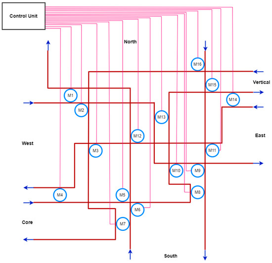
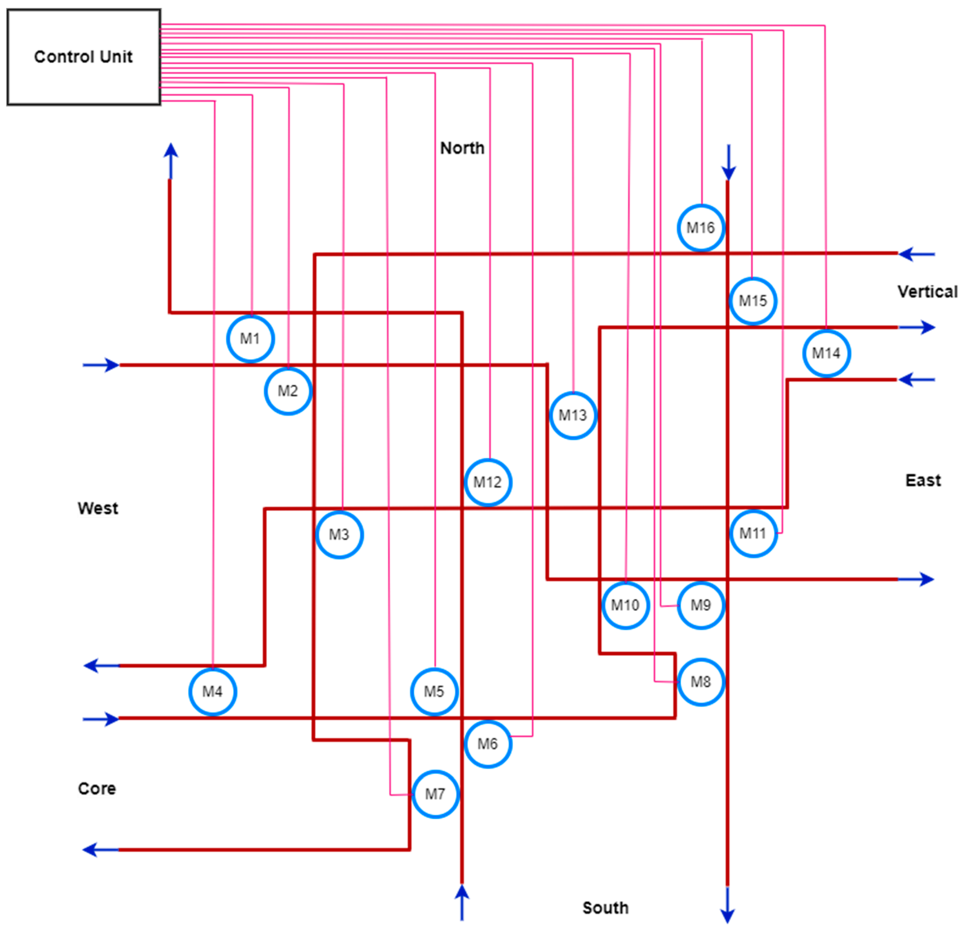
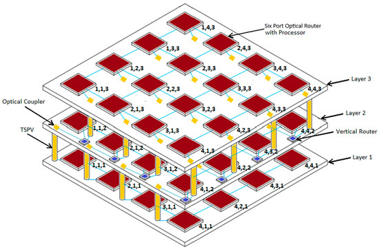
The proposed 3D ONoC comprises a multicore multilayer architecture with a U × V × W mesh topology. It consists of an electronic layer containing processing elements for control and a photonic layer for high-speed optical communication. Through-Silicon Photonic Vias (TSPVs) provide vertical optical connections between stacked layers. This architecture is a network of Intellectual Property (IP) cores linked via special optical routers arranged in a 4 × 4 × 3 mesh topology. To optimize communication efficiency, the architecture separates routing responsibilities: the Horizontal Dimension-Order Routing-Aware Router (HDORAR) handles intra-layer switching, and the Vertical Optical Router (VOR) handles inter-layer connections. The HDORAR is a six-port router that interconnects neighboring routers and a local core within the same layer. It utilizes an optimized internal fabric consisting of 14 waveguide crossings, 16 micro-ring resonators (MRRs), and 16 waveguide bends, as shown in Figure 1. This optimized router uses fewer components than conventional 3D routers [21]; hence, it reduces insertion loss and crosstalk accumulation [22,29,30].
Figure 1.
Horizontal Dimension-Order Routing-Aware Router (HDORAR).
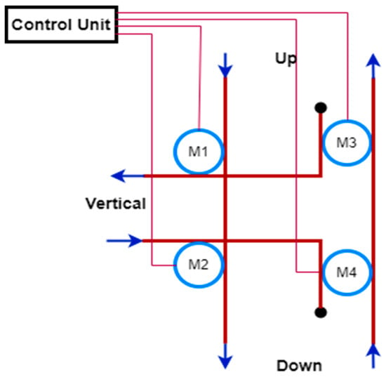
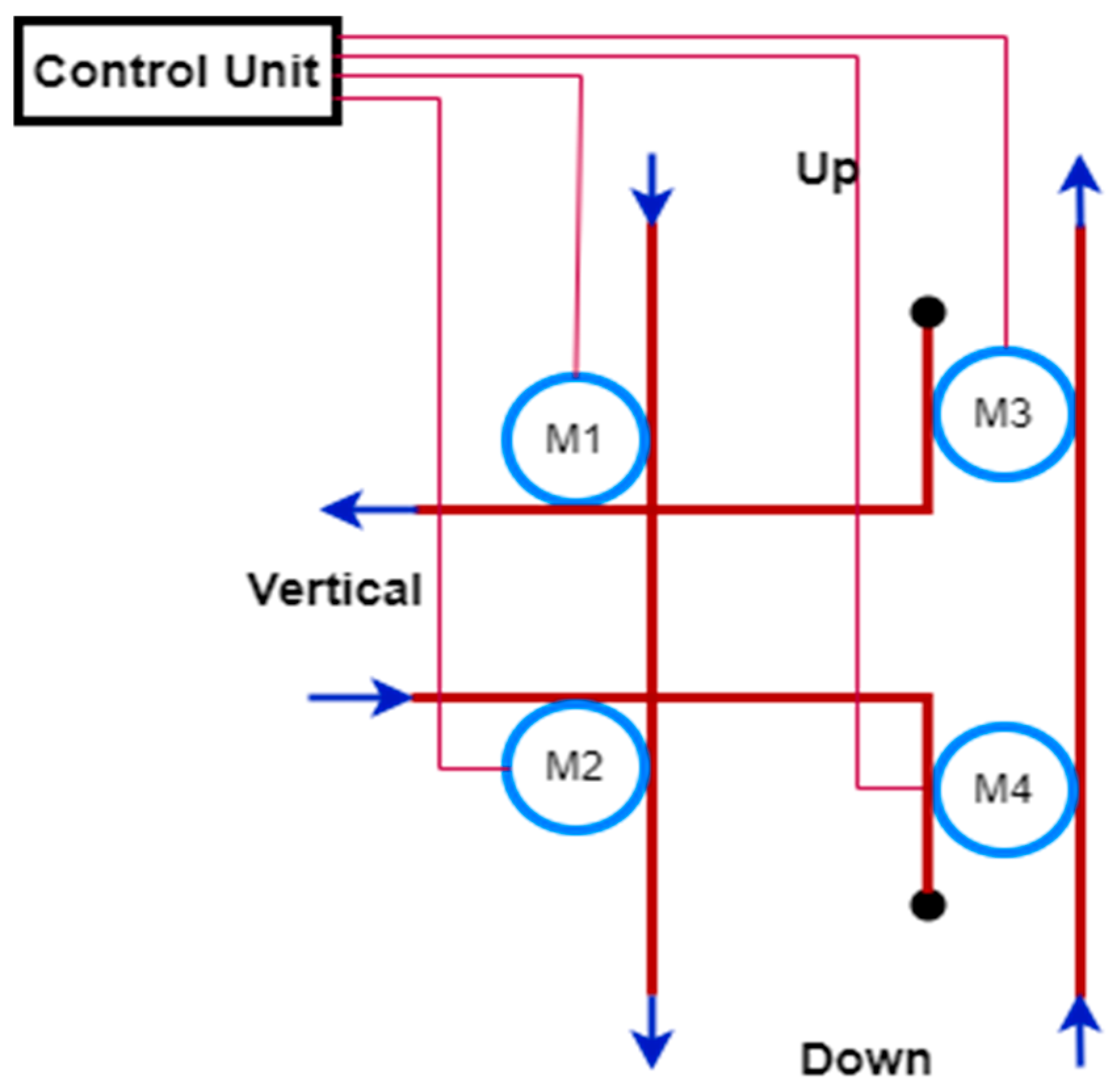
Minimizing these components is essential, as waveguide crossings and MRRs are primary sources of insertion loss and crosstalk noise. For vertical communication, the three-port VOR, as shown in Figure 2, interconnects routers across multiple layers. The vertical layer spacing is treated independently of the horizontal router pitch; each inter-layer transition includes a technology-dependent loss and, when required, a vertical crosstalk coefficient. Unlike conventional multi-port routers, the VOR is a simplified three-port router dedicated to inter-layer communication, which significantly reduces routing complexity and vertical insertion loss.
Figure 2.
Vertical Optical Router (VOR).
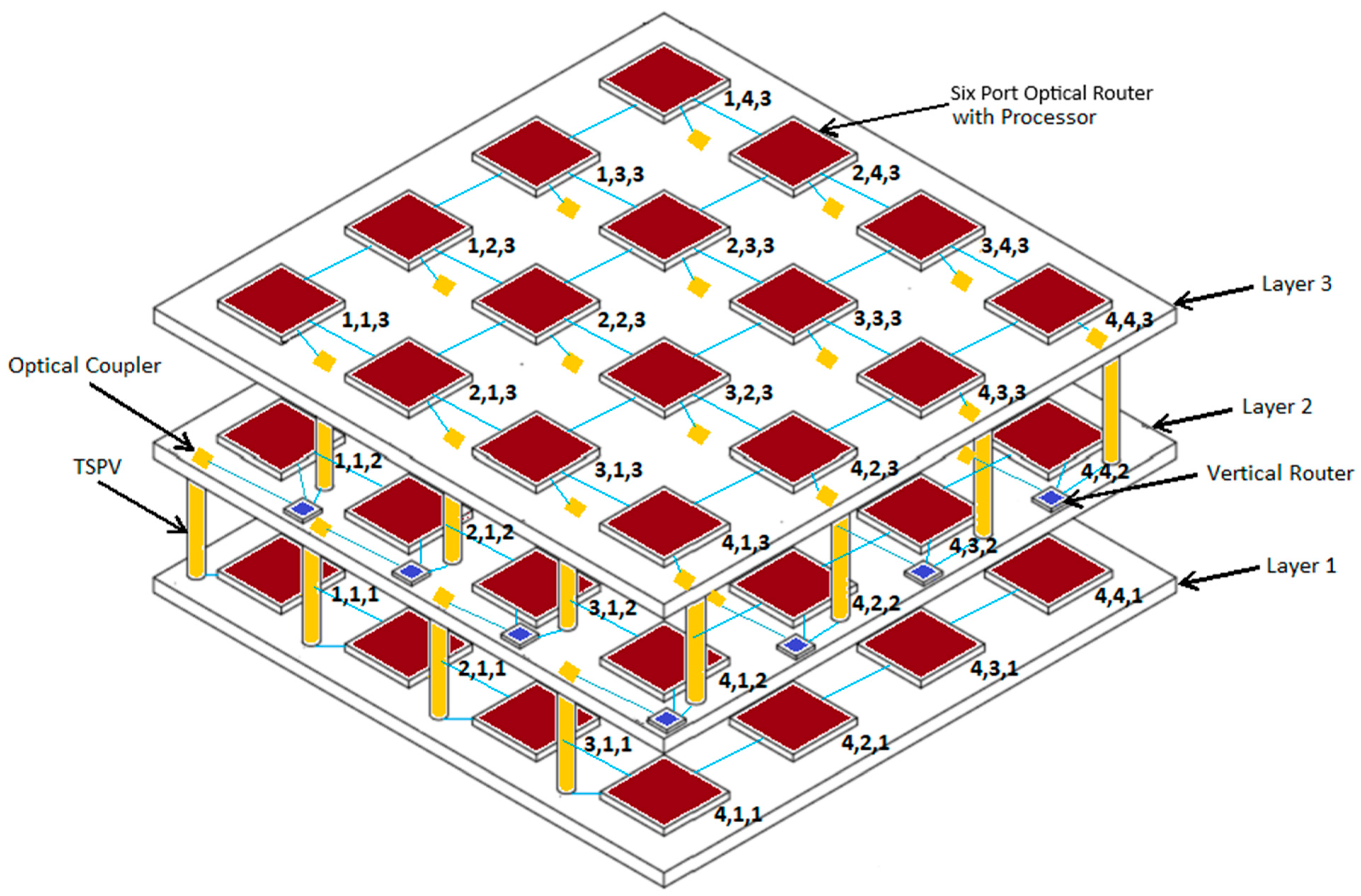
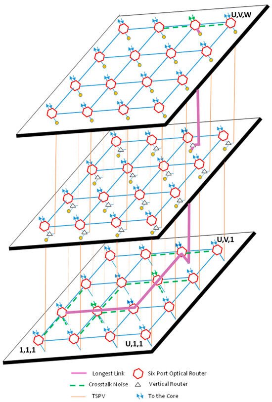
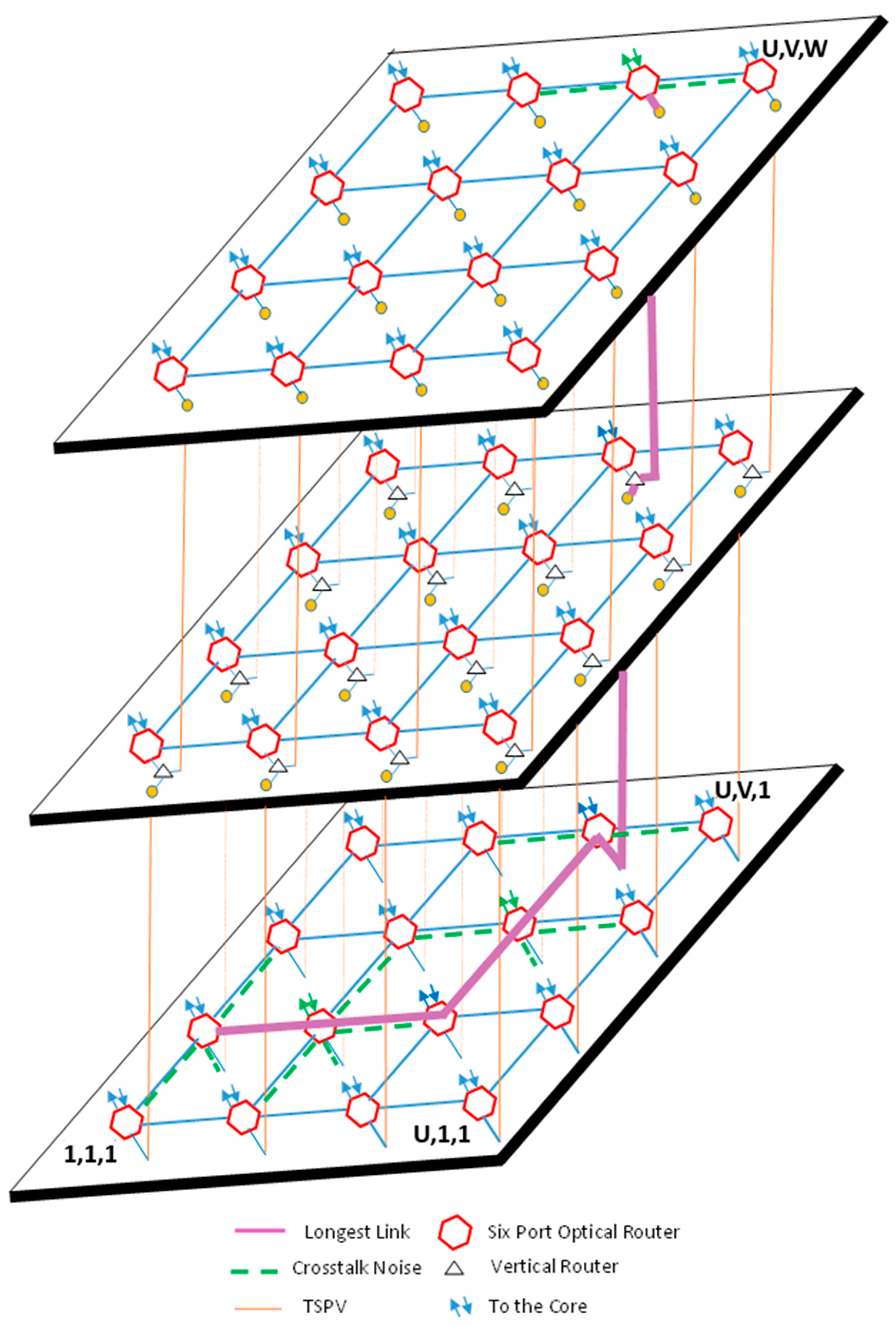
By integrating these routers, we create a novel 3D ONoC architecture for a 4 × 4 × 3 mesh topology, as shown in Figure 3. This architecture uses TSPVs to enable efficient vertical connectivity between multiple photonic layers. Existing 3D ONoC architectures reported in [23,27,28] use the same router for both intra-layer and inter-layer communication, whereas the proposed architecture separates these functions using HDORAR and VOR, reducing the number of photonic components and improving scalability.
Figure 3.
Architecture of 4 × 4 × 3 3D ONoC.
The system employs a hybrid switching approach in which the electronic control unit manages path setup, and the photonic path transmits high-speed optical data through the reserved path without buffering. This hybrid switching permits efficient path setup while maintaining high-speed optical data transmission. During setup, each hop reserves the requested output only if it is available. If the requested resource is busy, the source releases the partial reservations and retries after a random backoff interval. An end-to-end acknowledgment confirms the path before optical data transmission.
The XYZ dimension order routing algorithm governs path selection. In this work, non-blocking refers to admissible input–output paths inside the router fabric. Simultaneous end-to-end circuit requests can still contend for shared optical links. We implement XYZ routing using HDORAR for X–Y traversal and VOR for Z-direction communication. In the proposed architecture, there is a unique ID (a, b, c) to each processor, where a ϵ {1, 2, 3, … U}, b ϵ {1, 2, 3,…V}, c ϵ {1, 2, 3, … W}, and the same ID is used for its local router, which facilitates a straightforward addressing across the 3D grid.
To illustrate the operation, consider the longest path in a 4 × 4 × 3 network from processor (1,1,1) to (4,4,3). Initially, the control unit at the source node (1,1,1) generates a path-setup packet. After the receiver accepts it, the required MRRs along the path activate. The optical signal is then transmitted sequentially through the X-dimension to the router at (4,1,1), then switched into the Y-dimension until it arrives at (4,4,1). Finally, the VOR switches the data into the Z-dimension, moving it from the first layer to the third layer, where the optical router at (4,4,3) receives it and delivers it to the local processor. This example illustrates deterministic route construction; it does not imply zero contention for simultaneous network requests. The dimension-order approach ensures high-speed, reliable data movement while maintaining signal integrity across the interconnects.
3. Mathematical Modeling
The architectural diversity of 3D ONoCs requires mathematical models to enable accurate quantitative analysis. The performance of these networks is governed by their physical layer components, where the integration of optical waveguides, crossings, and MRRs introduces signal degradation. Consequently, we first perform comprehensive mathematical modeling at the router level and then at the network level to evaluate insertion loss, crosstalk noise, and SNR. The parameters used in this study are given in Table 1.
Table 1.
Parameters used for the study.
3.1. Mathematical Modeling for Performance of the Optical Router
This section details the modeling of a six-port optical router within a 3D ONoC. The ports are indexed as 0 (Core), 1 (West), 2 (North), 3 (East), 4 (South), and 5 (Vertical). The 3D ONoC considered for modeling has a general size of U × V × W. The horizontal and vertical inter-router links are treated separately. The first parameter considered is the insertion loss for the router R1() from the ith port to the jth port, and it is given as
where and H is the hop length, i.e., the length between the routers of ONoC. represents the insertion loss of router R1() from the ith port to jth port, given by
This loss includes switching loss and propagation loss for the waveguide length . For chip size c, the hop length for U × V × W ONoC is obtained by
The switching loss of an optical router from the input port to the output port is determined by the cumulative loss incurred by physical components along that specific internal path. Switching loss from the ith port to the jth port of the router is obtained using the number of waveguide crossings , the number of bends , the number of MRRs in the ON state , and the number of MRRs in the OFF state in the path and written as
where , , and represent bending loss, crossing loss, and insertion loss of MRR in the OFF state and the ON state, respectively. The resulting output power at the jth port of R1() when power input is applied is given by
where is the total insertion loss for the selected path. To accurately quantify signal degradation, the router’s operational status, , must be defined. The status of router R1() indicates whether optical data can be received on other ports while optical data is transferred from the ith port to the jth port, and is represented as . To understand this, assume are the input ports for the output ports respectively. The status for the east port to north port path indicates that optical signals are available at the north port, south port, and vertical port due to signal applied at the east port, west port, and south port, respectively. Here, −1 indicates that the signal is not available at that output port; therefore, the core, east, and west ports are free. This status is necessary to identify crosstalk noise in a particular router path. is the crosstalk noise added under the status to the optical signal traveling from the ith port to the jth port, and is given by
is the path crosstalk noise coefficient from the ith port to the jth port introduced by the input optical signal at the mth port in the optical router R1() under status, and it is written as
where is the waveguide loss, and kx is the crosstalk coefficient of the crossing waveguide or MRR. Linear transmission factors along the leakage path are shown in (7). In this work, we consider first-order crosstalk, and we do not explicitly consider power that leaks through another device. Higher-order crosstalk can be added recursively if it is considered.
3.2. Mathematical Modeling for Performance of 3D Optical Network-on-Chip
After developing the mathematical model for individual optical routers, the framework is extended to the 3D ONoC network level to enable system-wide reliability assessment. For a source-to-destination route P, the total insertion loss is the sum of the dB losses of the router paths, horizontal waveguide segments, and vertical transitions. In the U × V × W 3D ONoC, signal integrity is dictated by the cumulative effect of physical-layer degradations across multiple layers. At the network level, the source-to-destination insertion loss for the 3D ONoC is defined as the summation of the insertion losses of all routers encountered along the routing path in the X, Y, and Z dimensions:
where , , and represent the insertion losses of the router R1 for the s to d path in the x, y, and z directions, respectively. This model accounts for the hop length and the specific internal losses of the HDORAR and VOR architectures. Different paths in U × V × W ONoC with six-port and three-port optical routers for SNR analysis are considered. Because the ONoC has multiple layers, more paths are available for data transmission. We used four different longest paths, each with different possible crosstalk noise, to analyze the effect of insertion loss and crosstalk noise on the ONoC SNR.
- Path 1: Transmission from the processor of router R1(1,1,1) to the processor of router R1(U, V, W). As an outer-side path, it typically experiences the lowest cumulative crosstalk noise.
- Path 2: Transmission from the processor of router R1(1,1,1) to the processor of router R1(U − 1, V, W).
- Path 3: Transmission from the processor of router R1(1,2,1) to the processor of router R1(U, V, W).
- Path 4: Transmission from the processor of router R1(1,2,1) to the processor of router R1(U − 1, V, W). Being an inner-side path, it is subjected to the highest crosstalk noise due to the high density of surrounding active waveguides and routers.
While mathematical models are developed for all four paths, this work presents a detailed analysis of Path 4 to demonstrate the worst-case performance scenario. The modeling process begins with a generalized mathematical framework. It is subsequently refined by applying the specific physical parameters of the HDORAR and VOR architectures, including their optimized counts of waveguide crossings and MRRs. This can be extended for any path in a similar 3D ONoC.
Network-level performance is ultimately determined by the SNR, the ratio of received signal power to accumulated noise power at the destination node. The SNR for the fourth path is given by
Moreover, the Bit Error Rate (BER) is a critical metric for assessing ONoC reliability, as it is directly dictated by the SNR and cumulative crosstalk noise. For an On-Off Keying Non-Return to Zero (OOK-NRZ) modulation scheme, the BER is modeled as
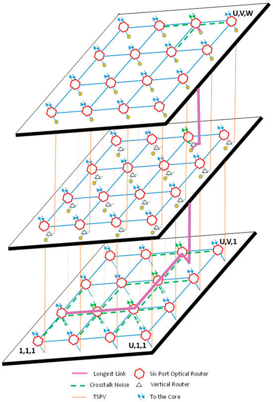
The signal power is derived by applying the network-level insertion loss to the input power, while the noise power is the summation of all first-order crosstalk (and potentially infinite-order crosstalk) leaked into the primary signal path from concurrent data streams. Using XYZ dimension-order routing, this modeling approach enables quantitative assessment of any transmission path within the 3D ONoC, ensuring the architecture meets stringent Bit Error Rate (BER) requirements for reliable high-speed computing. Figure 4 illustrates the fourth transmission path within the 4 × 4 × 3 3D ONoC architecture, and in this diagram:
Figure 4.
Fourth path of 3D ONoC.
- ▪
- Red hexagons represent the six-port intra-layer routers (HDORAR).
- ▪
- Black triangles denote the three-port vertical routers (VOR) used for inter-layer communication.
- ▪
- Vertical orange lines indicate the TSPVs that interconnect the layers.
- ▪
- The solid violet line traces the primary signal path.
- ▪
- Green dotted lines indicate crosstalk noise propagation from concurrent data transmissions.
The diagram highlights the inner-side path from processor R1(1,2,1) to R1(U − 1, V, W), modeled specifically to analyze the effects of high-intensity crosstalk and insertion loss on the system’s SNR.
Crosstalk noise generated in the routers of the fourth path (R1(1,2,1) to R1(U − 1, V, W)) under status is represented by . So, crosstalk noise from the ith port to the jth port for the whole path is obtained as below:
For
For
For
For
For
For
For
For
Noise power in the fourth path is obtained using crosstalk noise and insertion loss in the path and is given by
Signal power at the output port of the last router in the path can be obtained using input power and insertion loss and written as
3.3. Mathematical Model of Fourth Path Using HDORAR and VOR
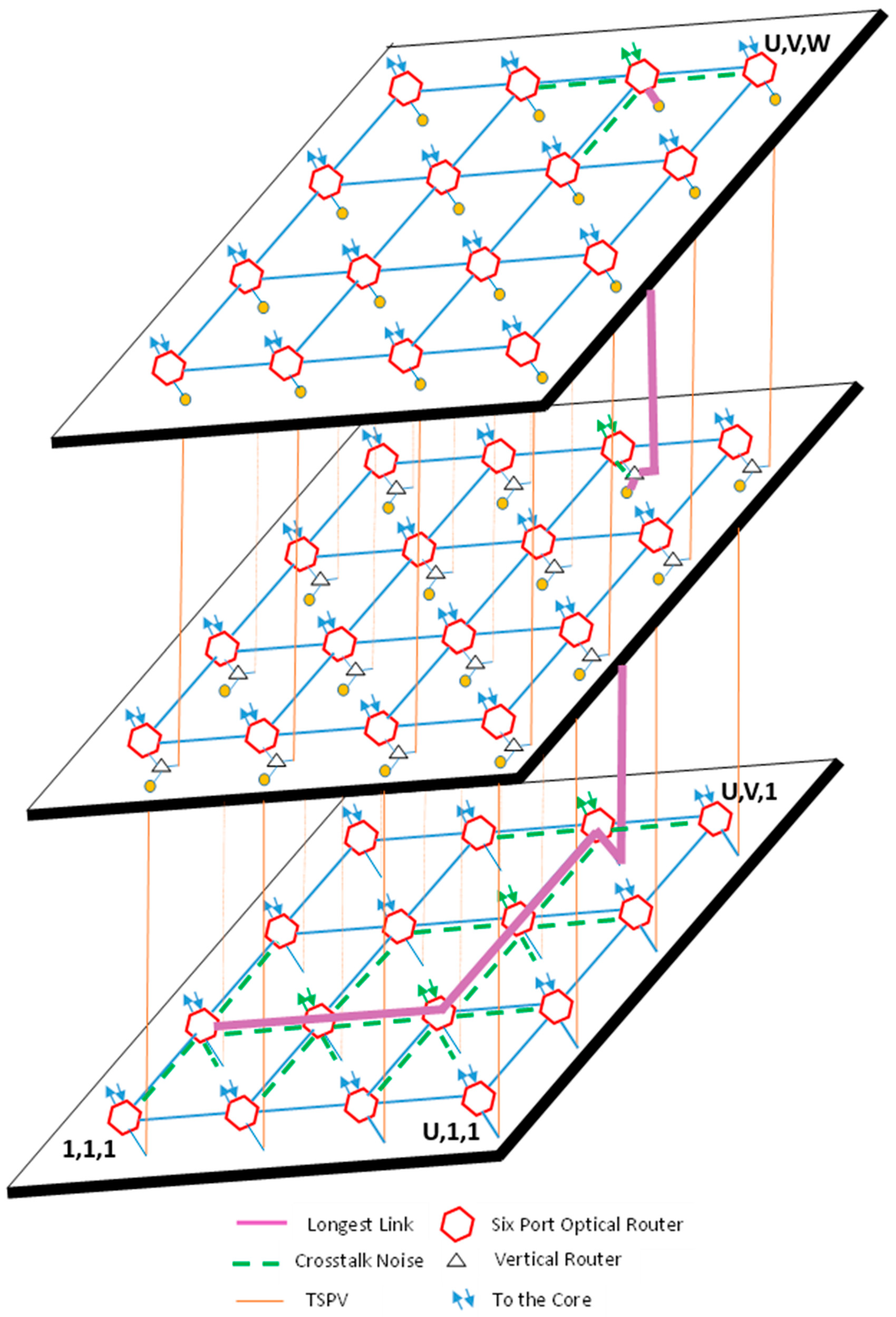
The general mathematical model of the 3D ONoC is applied to the ONoC designed using the HDORAR and VOR. The fourth path is used to model crosstalk noise and SNR. Figure 5 shows the fourth-longest path along with crosstalk noise at various locations in the HDORAR- and VOR-based 3D ONoC. The crosstalk noise for this path at various locations is written below as . It is evident that, due to the efficient design of optical routers, crosstalk noise at some locations in the path is reduced to zero.
Figure 5.
Fourth path of 3D ONoC using HDORAR and VOR.
For
For
For
For
For
For
For
For
Noise power in the fourth path is given by
where
and
4. Quantitative Analysis of 3D Optical Networks-on-Chip
The operational efficiency and reliability of the proposed 3D ONoC architecture are evaluated through a rigorous quantitative analysis of key physical-layer metrics: insertion loss, crosstalk noise, and SNR. To determine the architecture’s scalability and performance limits, we calculate the worst-case insertion loss for the longest data transmission paths across various network dimensions and compare them. The reported results are physical-layer scaling for selected paths.
4.1. Insertion Loss Analysis
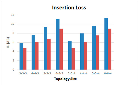
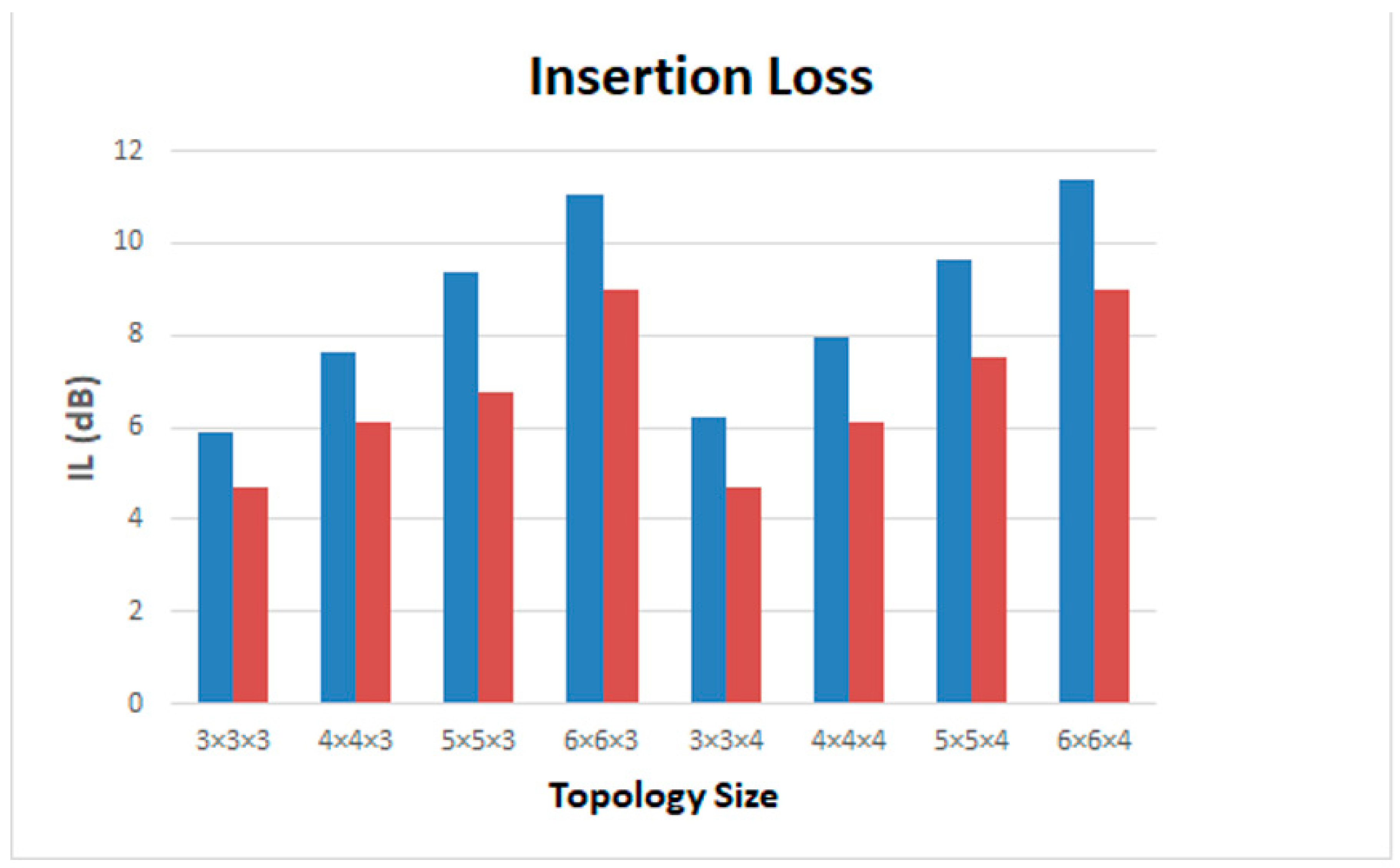
The 3D mesh structure, using the HDORAR for intra-layer switching and the VOR for inter-layer connectivity, was considered for insertion-loss analysis. Insertion loss is critical because it directly determines the minimum optical power required from the laser source to meet the photodetector’s sensitivity and maintain a target BER. As shown in Figure 6, the insertion loss increases with the topology size due to the increased number of waveguide crossings, bends, and MRRs along the transmission path.
Figure 6.
Insertion loss for different topology sizes using the proposed HDORAR-based 3D ONoC (red) and the method reported in [27] (blue).
For a 3 × 3 × 3 ONoC, the proposed design achieves an insertion loss of 4.70 dB, whereas the architecture in [27] incurs a loss of 5.90 dB. For a larger 6 × 6 × 4 topology, the proposed architecture exhibits 8.96 dB of loss compared to 11.37 dB for the design in [27]. In a vertical expansion from a 3 × 3 × 3 to a 3 × 3 × 4 topology, the proposed design shows a negligible increase in loss (from 4.706 dB to 4.707 dB). In contrast, the conventional design increases from 5.905 dB to 6.215 dB. This demonstrates that the three-port VOR effectively mitigates the signal degradation in inter-layer communication.
At the network level, the results show that, for scalable solutions, 3D integration offers more advantages than 2D expansion. For example, a 6 × 6 × 3 topology (108 cores) generates an insertion loss of 8.966 dB, while a 5 × 5 × 4 topology (100 cores) results in only 7.547 dB. This shows that layer-based expansion is architecturally superior to adding processing elements horizontally, as it reduces hops and physical components in the primary signal path. Overall, the proposed architecture using HDORAR and VOR achieves an average insertion-loss reduction of 31.28% compared to traditional 3D ONoC designs.
4.2. Worst-Case SNR Analysis for 3D ONoC
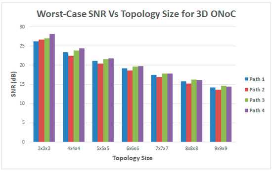
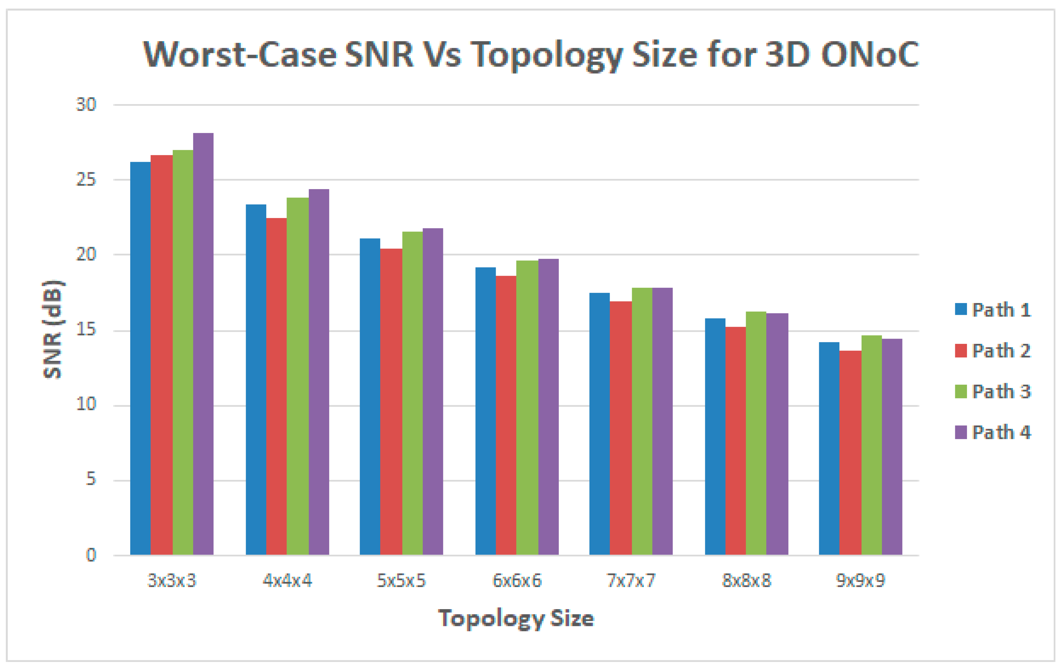
We conducted the worst-case SNR analysis for the four identified longest transmission paths across different ONoC dimensions. Path 4 is a constructed first-order crosstalk stress case rather than a traffic-average worst case; the reported plots do not include higher-order leakage. Figure 7 illustrates that, for smaller network sizes, Path 1 has the lowest SNR because it is the physically longest link. As the ONoC topology scales, the SNR for all paths reduces as the number of active waveguide crossings and MRRs increases. Although Path 1 maintains the highest insertion loss across all paths, its SNR becomes relatively better than other paths in larger networks. This is because it is an outer-side path and experiences significantly lower cumulative crosstalk interference than inner-side paths like Path 4, which is subjected to noise from a higher density of surrounding active components. These results show that as 3D ONoC density increases, crosstalk noise, including higher-order noise, eventually becomes the primary bottleneck for communication reliability.
Figure 7.
Worst-case SNR versus topology size for proposed 3D ONoC.
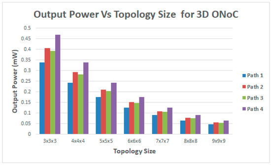
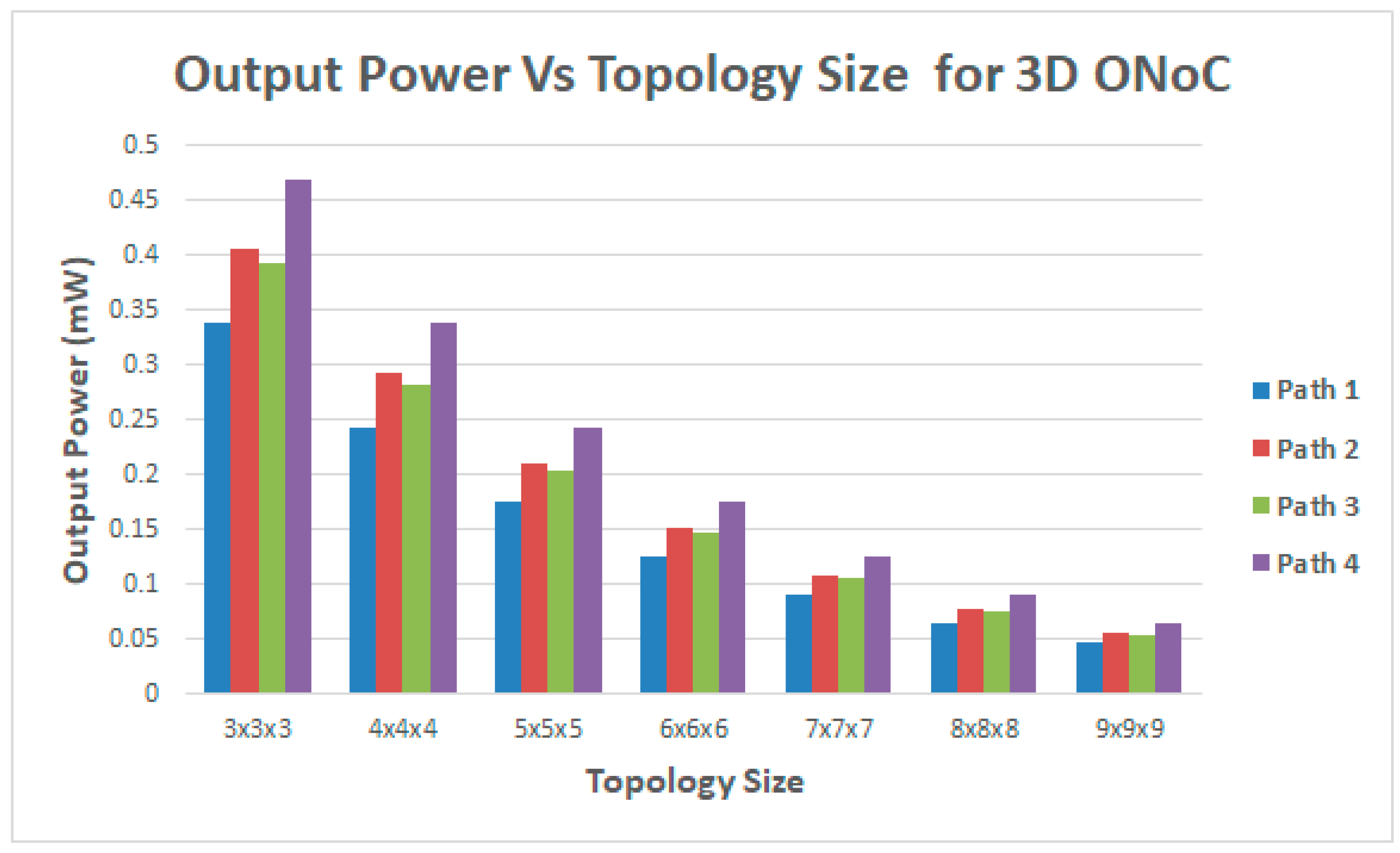
Figure 8 shows the output power obtained at the destination nodes for each selected path for different 3D ONoC dimensions. Path 1 exhibits the minimum output power because it incurs the highest cumulative insertion loss, whereas Path 4 has the highest output power among the four longest paths, reflecting low signal losses.
Figure 8.
Output power vs. topology size for proposed 3D ONoC.
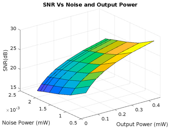
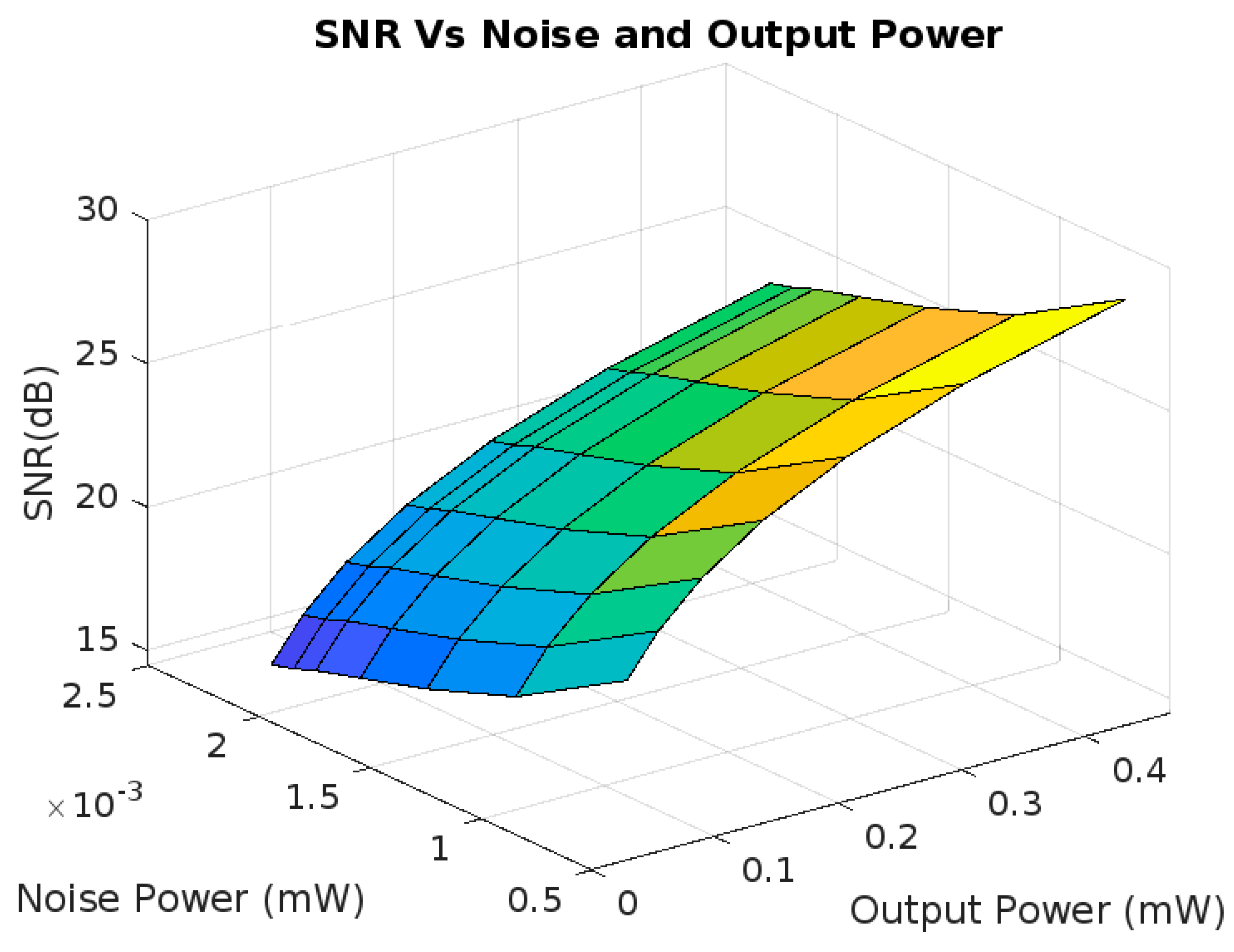
Figure 9 illustrates the SNR performance of the proposed 3D ONoC relative to output power and noise power for Path 4. For HDORAR- and VOR-based architectures, signal attenuation is reduced while maintaining lower crosstalk noise, ultimately resulting in a superior SNR across 3D data paths.
Figure 9.
SNR vs. noise and output power in 3D ONoC.
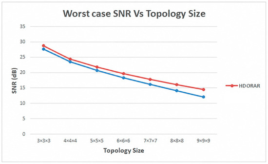
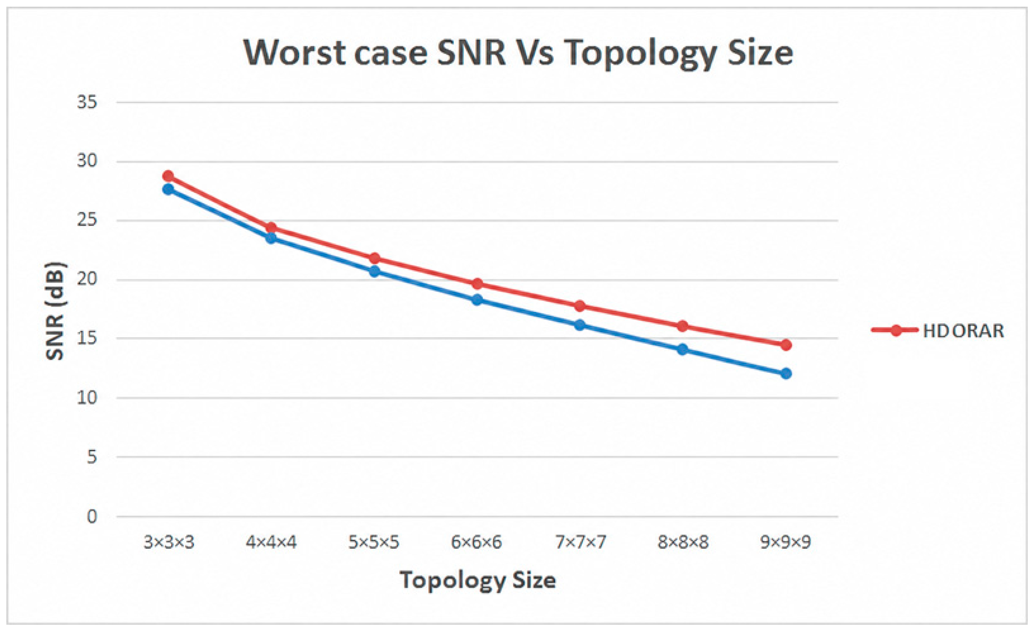
Figure 10 shows the comparison of worst-case SNR for different sizes of 3D ONoCs. The worst-case SNR of the ONoC with HDORAR and VOR is compared with an ONoC designed based on the router presented in [3], which has the lowest insertion loss among routers reported in the literature. The performance of both ONoCs is nearly similar for a lesser number of cores. As the number of cores increases, the proposed ONoC outperforms the others, showing a 9.23% improvement in worst-case SNR.
Figure 10.
Worst-case SNR versus number of cores for the proposed HDORAR-based 3D ONoC (red) compared with the method reported in [27] (blue).
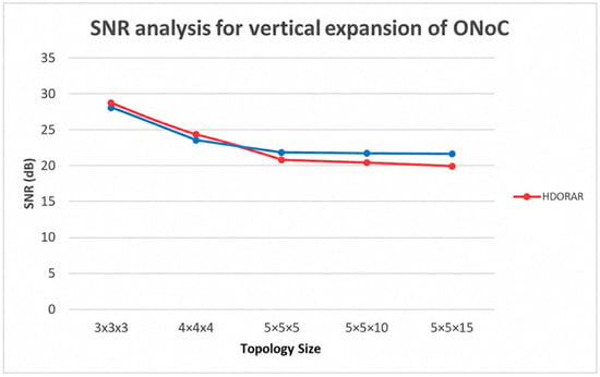
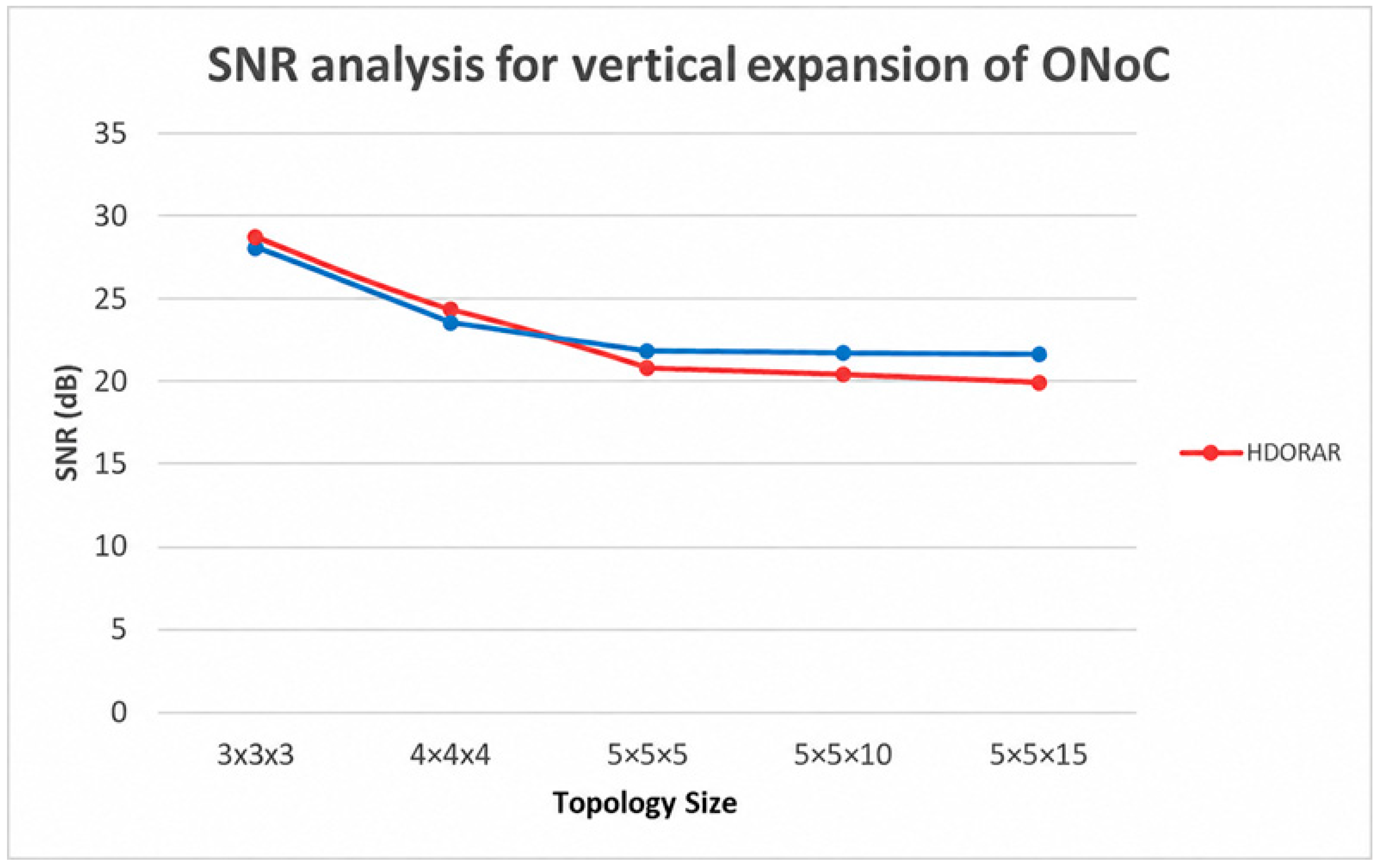
The SNR for an ONoC of size 7 × 7 × 7 (343 cores) is 17.8235 dB, while for 5 × 5 × 15 (375 cores), it is 21.6161 dB. It shows that vertical expansion provides superior performance and compactness compared to horizontal scaling for high-density ONoCs. Figure 11 shows that the proposed architecture improves the SNR by 12.38% over traditional designs, highlighting the efficiency of the VOR in vertical connectivity while maintaining a more compact physical footprint. These values indicate a favorable vertical-scaling trend. The real stacked implementation may add technology-dependent TSPV/inter-layer losses.
Figure 11.
SNR for vertical expansion of the proposed HDORAR-based 3D ONoC (red) compared with the method reported in [27] (blue).
A comparative BER analysis was conducted to evaluate the communication reliability of the proposed 3D ONoC against the benchmark architecture. For the selected topology, the proposed design achieves a BER of 3.58 × 10⁻¹⁰ for a 5 × 5 × 5 size, significantly outperforming the benchmark BER of 2.52 × 10⁻⁸.
We further investigated the impact of vertical scaling by increasing the core count along the Z-dimension. For the 5 × 5 × 25 configuration, the proposed ONoC maintains a superior BER of 4.26 × 10⁻¹⁰ while the design results in a BER of 9.15 × 10⁻⁹. These results demonstrate that the proposed architecture effectively meets high-fidelity communication requirements.
5. Conclusions
This work introduced a novel 3D ONoC architecture that effectively addresses the scalability and communication bottlenecks of modern MPSoCs by utilizing a bifurcated router design. Developing the six-port HDORAR for intra-layer switching and the three-port VOR for inter-layer connectivity provides a more compact, less complex alternative to unified router structures. We develop detailed mathematical models for various performance metrics. The results demonstrate significant performance gains, with the proposed design achieving a 31.28% reduction in average insertion loss and a 9.23% improvement in worst-case SNR. The study also shows that vertical expansion of ONoCs outperforms horizontal scaling, maintaining higher SNR and BER with a smaller physical footprint and enabling practical implementation of reliable, energy-efficient, high-performance interconnects for future all-optical computing environments.
Author Contributions
Conceptualization, B.S.C., P.D.K. and N.B.J.; methodology, B.S.C., P.D.K. and N.B.J.; validation, N.B.J. and B.S.C.; formal analysis, N.B.J., B.S.C. and P.D.K.; investigation, N.B.J., B.S.C. and P.D.K.; resources, and data curation, N.B.J., B.S.C. and P.D.K.; writing—original draft preparation, N.B.J.; writing—review and editing, B.S.C. and P.D.K.; visualization, N.B.J.; supervision, B.S.C. and P.D.K. All authors have read and agreed to the published version of the manuscript.
Funding
This research received no external funding.
Data Availability Statement
The original contributions presented in this study are included in the article. Further inquiries can be directed to the corresponding author.
Conflicts of Interest
The authors declare no conflicts of interest.
References
- Salloum, C.E.; Elshuber, M.; Höftberger, O.; Isakovic, H.; Wasicek, A. The ACROSS MPSoC—A New Generation of Multi-Core Processors Designed for Safety-Critical Embedded Systems. In Proceedings of the 2012 15th Euromicro Conference on Digital System Design; IEEE: Cesme, Turkey, 2012; pp. 105–113. [Google Scholar]
- Miller, D. Device Requirements for Optical Interconnects to Silicon Chips. Proc. IEEE 2009, 97, 1166–1185. [Google Scholar] [CrossRef] [Scilit]
- Zhang, Z.; Colle, D.; Tavernier, W.; Pickavet, M. On the Network Design and Control of an Optical Network: Interconnecting Multiple Chips on a Wafer. J. Opt. Commun. Netw. 2023, 15, 119. [Google Scholar] [CrossRef] [Scilit]
- Chen, Z.; Gu, H.; Yang, Y.; Bai, L.; Li, H. A Power Efficient and Compact Optical Interconnect for Network-on-Chip. IEEE Comput. Arch. Lett. 2014, 13, 5–8. [Google Scholar] [CrossRef] [Scilit]
- Li, B.; Li, J.; Zhao, Y.; Lin, X.; Chua, S.-J.; Miao, L.; Fitzgerald, E.A.; Lee, M.L.; Chaudhari, B.S. Ultracompact, Multifunctional, and Highly Integrated 3×2 Photonic Switches. Appl. Phys. Lett. 2004, 84, 2241–2243. [Google Scholar] [CrossRef] [Scilit]
- Nikdast, M.; Xu, J.; Duong, L.H.K.; Wu, X.; Wang, X.; Wang, Z.; Hao, Q. Crosstalk Noise in WDM-Based Optical Networks-on-Chip: A Formal Study and Comparison. IEEE Trans. VLSI Syst. 2015, 23, 2552–2565. [Google Scholar] [CrossRef] [Scilit]
- Yang, B.; Li, Y.; Xi, C.; Shan, R.; Feng, Y.; Luo, J. Design and Implementation of Reconfigurable Array Adaptive Optoelectronic Hybrid Interconnect Shunting Network. Electronics 2024, 13, 1668. [Google Scholar] [CrossRef] [Scilit]
- Ji, R.; Yang, L.; Zhang, L.; Tian, Y.; Ding, J.; Chen, H.; Lu, Y.; Zhou, P.; Zhu, W. Five-Port Optical Router for Photonic Networks-on-Chip. Opt. Express 2011, 19, 20258. [Google Scholar] [CrossRef] [Scilit]
- Gu, H.; Mo, K.H.; Xu, J.; Zhang, W. A Low-Power Low-Cost Optical Router for Optical Networks-on-Chip in Multiprocessor Systems-on-Chip. In 2009 IEEE Computer Society Annual Symposium on VLSI; IEEE: New York, NY, USA, 2009; pp. 19–24. [Google Scholar]
- Chaudhari, B.S.; Patil, S.S. Optimized Designs of Low Loss Non-Blocking Optical Router for ONoC Applications. Int. J. Inf. Technol. 2020, 12, 91–96. [Google Scholar] [CrossRef] [Scilit]
- Shi, X.; Wu, N.; Ge, F.; Yan, G.; Xing, Y.; Ma, X. Srax: A Low Crosstalk and Insertion Loss 5×5 Optical Router for Optical Network-on-Chip. In IECON 2019—45th Annual Conference of the IEEE Industrial Electronics Society; IEEE: Lisbon, Portugal, 2019; pp. 3102–3105. [Google Scholar]
- Asadi, Y. Optical Network-on-Chip (ONoC) Architectures: A Detailed Analysis of Optical Router Designs. J. Semicond. 2024, 46, 031401–031436. [Google Scholar] [CrossRef] [Scilit]
- Jadhav, N.B.; Chaudhari, B.S.; Khandekar, P. SNR Modeling and Analysis for Two Dimensional and Three Dimensional ONoC. In 2023 IEEE 8th International Conference for Convergence in Technology (I2CT); IEEE: Lonavla, India, 2023; pp. 1–5. [Google Scholar]
- Dai, L.; Su, Y.; Xie, Y. A Novel Torus-Based Optical Networks-on-Chip Exploiting Double Path Communication Algorithm. In Second International Conference on Electronic Information Engineering, Big Data, and Computer Technology (EIBDCT 2023); Kong, X., Ed.; SPIE: Xishuangbanna, China, 2023; p. 51. [Google Scholar]
- Xie, Y.; Zhao, W.-L.; Xu, W.-H.; Huang, Y.-X.; Zhang, Z.-D. Performance Optimization and Evaluation for Mesh-Based Optical Networks-on-Chip. IEEE Photonics J. 2015, 7, 7801412. [Google Scholar] [CrossRef] [Scilit]
- Nikdast, M.; Xu, J.; Duong, L.H.K.; Wu, X.; Wang, Z.; Wang, X.; Wang, Z. Fat-Tree-Based Optical Interconnection Networks Under Crosstalk Noise Constraint. IEEE Trans. VLSI Syst. 2015, 23, 156–169. [Google Scholar] [CrossRef] [Scilit]
- Xie, Y.; Xu, W.; Zhao, W.; Huang, Y.; Song, T.; Guo, M. Performance Optimization and Evaluation for Torus-Based Optical Networks-on-Chip. J. Light. Technol. 2015, 33, 3858–3865. [Google Scholar] [CrossRef] [Scilit]
- Su, Y.; Xie, Y.; Liu, W.; Chen, Z.; Jiang, X.; Li, L.; Ye, Y.; Xu, F. A Novel MDM-Based Optical Networks-on-Chip with Reliability Analysis. IEEE Trans. Comput.-Aided Des. Integr. Circuits Syst. 2026, 45, 1290–1303. [Google Scholar] [CrossRef] [Scilit]
- Li, B.; Chua, S.-J.; Fitzgerald, E.A.; Chaudhari, B.S.; Jiang, S.; Cai, Z. Intelligent Integration of Optical Power Splitter with Optically Switchable Cross-Connect Based on Multimode Interference Principle in SiGe∕Si. Appl. Phys. Lett. 2004, 85, 1119–1121. [Google Scholar] [CrossRef] [Scilit]
- Zhu, K.; Gu, H.; Yang, Y.; Tan, W.; Zhang, B. A 3D Multilayer Optical Network on Chip Based on Mesh Topology. Photonic Netw. Commun. 2016, 32, 293–299. [Google Scholar] [CrossRef] [Scilit]
- Gu, H.; Xu, J. Design of 3D Optical Network on Chip. In 2009 Symposium on Photonics and Optoelectronics; IEEE: New York, NY, USA, 2009; pp. 1–4. [Google Scholar]
- Ye, Y.; Xu, J.; Huang, B.; Wu, X.; Zhang, W.; Wang, X.; Nikdast, M.; Wang, Z.; Liu, W.; Wang, Z. 3-D Mesh-Based Optical Network-on-Chip for Multiprocessor System-on-Chip. IEEE Trans. Comput.-Aided Des. Integr. Circuits Syst. 2013, 32, 584–596. [Google Scholar] [CrossRef] [Scilit]
- Fadhel, M.; Gu, H.; Wei, W. DORR: A DOR-Based Non-Blocking Optical Router for 3D Photonic Network-on-Chips. IEICE Trans. Inf. Syst. 2021, 104, 688–696. [Google Scholar] [CrossRef] [Scilit]
- Guo, P.; Hou, W.; Guo, L. A Low Insertion Loss and Non-Blocking Optical Router for 3D Optical Network-on-Chip (Invited Paper). In Asia Communications and Photonics Conference 2016; OSA: Wuhan, China, 2016; p. AS1E.2. [Google Scholar]
- Thirumaran, S.; Dhanabalan, S.S.; Sannasi, I.G. Design and Analysis of Photonic Crystal Ring Resonator Based 6 × 6 Wavelength Router for Photonic Integrated Circuits. IET Optoelectron. 2021, 15, 40–47. [Google Scholar] [CrossRef] [Scilit]
- Hou, W.; Guo, L.; Cai, Q.; Zhu, L. 3D Torus ONoC: Topology Design, Router Modeling and Adaptive Routing Algorithm. In 2014 13th International Conference on Optical Communications and Networks (ICOCN); IEEE: Suzhou, China, 2014; pp. 1–4. [Google Scholar]
- Guo, P.; Hou, W.; Guo, L.; Yang, Q.; Ge, Y.; Liang, H. Low Insertion Loss and Non-Blocking Microring-Based Optical Router for 3D Optical Network-on-Chip. IEEE Photonics J. 2018, 10, 7901010. [Google Scholar] [CrossRef] [Scilit]
- Guo, P.; Hou, W.; Guo, L.; Sun, W.; Liu, C.; Bao, H.; Duong, L.H.K.; Liu, W. Fault-Tolerant Routing Mechanism in 3D Optical Network-on-Chip Based on Node Reuse. IEEE Trans. Parallel Distrib. Syst. 2020, 31, 547–564. [Google Scholar] [CrossRef] [Scilit]
- Ma, X.; Li, B.; Chaudhari, B.S. Fabrication and Annealing Analysis of Three-Dimensional Photonic Crystals. Appl. Surf. Sci. 2007, 253, 3933–3936. [Google Scholar] [CrossRef] [Scilit]
- Xiao, M.; Tseng, T.-M.; Schlichtmann, U. Crosstalk-Aware Automatic Topology Customization and Optimization for Wavelength-Routed Optical NoCs. IEEE Trans. Comput.-Aided Des. Integr. Circuits Syst. 2022, 41, 5261–5274. [Google Scholar] [CrossRef] [Scilit]

Disclaimer/Publisher’s Note: The statements, opinions and data contained in all publications are solely those of the individual author(s) and contributor(s) and not of MDPI and/or the editor(s). MDPI and/or the editor(s) disclaim responsibility for any injury to people or property resulting from any ideas, methods, instructions or products referred to in the content. |
© 2026 by the authors. Licensee MDPI, Basel, Switzerland. This article is an open access article distributed under the terms and conditions of the Creative Commons Attribution (CC BY) license.