


Abstract
Two-dimensional (2D) materials are promising candidates for nanoscale wear-protective coatings. The mechanisms governing their tribological behaviour (i.e., friction and wear) are material-dependent. In this work, we use atomistic molecular dynamics simulations to investigate nanoscale sliding, friction, and lithographic tracks in two 2D materials, graphene and MoS2, both placed on a SiO2 substrate. Our results reveal fundamentally different deformation mechanisms in the two materials, where deformation comes as a consequence of applied normal load. MoS2 deforms via the formation of a stable out-of-plane pucker beneath the contact, enabling efficient absorption and elastic redistribution of mechanical energy within the coating as well as simultaneous reduction of plastic deformation of the underlying material. Wear prevention in the substrate comes at the cost of localised damage to the MoS2 layer along the sliding path once it reaches the rupture point. On the contrary, graphene exhibits strongly localised deformation due to its high in-plane stiffness and atomic thickness, leading to plastic deformation of the underlying material and mitigating layer damage. These findings provide clear design guidelines for 2D coatings in nanotribological applications, and highlight layered materials, such as MoS2, as particularly effective for wear protection.
1. Introduction
Reducing friction and wear between sliding interfaces in mechanical systems remains a significant challenge across all length scales, due to the complex interplay of contact mechanics, material properties, and surface phenomena—from atomistic to macroscopic levels [1,2,3]. The need for low friction and anti-wear performance of materials becomes particularly important when characteristic dimensions approach the micro- and nanoscale, where contact effects and surface forces dominate tribological behaviour [4,5]. At these length scales, conventional liquid lubricants often become ineffective due to the confinement effects, volatility, chemical instability, and similar factors [6,7,8]. Such shortcomings have sparked significant research interest in robust, atomically thin protective coatings that can withstand high contact stresses while maintaining low friction. In this context, two-dimensional (2D) materials, especially graphene [9,10,11,12] and molybdenum disulfide (MoS2) [13,14,15,16,17], have emerged as promising candidates for wear protection and solid lubrication at the nanoscale.
Graphene, a single atomic layer of -bonded carbon atoms arranged in a hexagonal lattice, combines exceptional in-plane stiffness and strength with low interlayer shear resistance in multilayer assemblies [18,19,20]. These nanomechanical properties distinguish graphene as an attractive ultra-thin protective coating for reducing friction and mitigating wear. Atomic Force Microscopy (AFM) experimental studies have shown that graphene exhibits distinct wear regimes as a function of the applied normal load [21,22]. At lower loads, graphene undergoes plastic deformation, but remains continuous. On the other hand, at higher loads, graphene fractures, tears, and eventually detaches from the substrate, consequently exposing the underlying substrate material. Importantly, the tribological performance of graphene strongly depends on its thickness: while single- and bilayer graphene can enhance the load-carrying capacity of the substrate, effective wear protection is achieved only with multilayer graphene films with a thickness of several nanometers [23]. Beyond its role as a passive protective layer, graphene also exhibits remarkable resistance to localised mechanical manipulations. AFM experiments on dynamic ploughing and scratching have revealed that graphene can withstand substantial local stresses before rupture, with deformation and cutting processes governed by the applied force and tip–sample interaction [24,25]. These studies provide valuable insights into the nanoscale mechanical response of graphene, including strain accumulation, fracture initiation, and material removal mechanisms, which are directly relevant to understanding wear in graphene under nanoscale sliding [23,24,25].
Molybdenum disulfide (MoS2) is another prominent 2D material, recognised also for its superior solid lubrication properties [26,27,28]. Its lamellar crystal structure, composed of weakly interacting S–Mo–S layers, facilitates interlayer sliding and results in low shear strength [29,30]. Analogous to graphene, MoS2 can act as a sacrificial layer that accommodates shear, thereby protecting the underlying substrate from damage. While graphene offers exceptional mechanical strength and chemical inertness, MoS2 provides intrinsically low shear resistance, making the comparison between these two materials particularly relevant for nanoscale wear protection strategies.
A detailed understanding of the wear mechanisms, thickness dependence, and failure modes of graphene and MoS2 at the nanoscale is therefore essential for the study of nanotribology of 2D layered materials. Such knowledge enables the rational design of advanced protective coatings and solid lubricants for micro- and nano-electromechanical systems (MEMSs and NEMSs) [31,32,33,34] and also allows understanding the mechanical behaviour of more complex systems involving 2D materials with adsorbed or intercalated small molecules [35,36].
2. Materials and Methods
All simulations presented in this work use the classical molecular dynamics (MD) method as implemented in the Large-scale Atomic/Molecular Massively Parallel Simulator (LAMMPS) [37,38]. In the system description, each atomic type is defined by its Lennard-Jones (LJ) parameters and charge. To capture all the relevant phenomena, we chose the all-atom level of description of materials (i.e., All-Atom MD simulations) [36,39,40,41,42,43,44,45]. The MD simulation setup reproduces nanoscale deformation, friction, and wear processes in 2D materials on oxide substrates, similar to conditions in AFM nano-lithography and friction force manipulation experiments [24,46,47,48]. We fully leveraged parallel simulation by running a batch submission script suitable for High-Performance Computing (HPC) environments. A velocity–Verlet algorithm with a time step of 0.5 fs allowed numerical stability of the equations of motion in high-load contact during sliding.
In the following, we provide an overview of pair- and many-body-bond-order potentials used to describe covalently bonded and layered materials. Tersoff-type potential parametrised for silicon–oxygen systems enabled realistic modelling of elastic deformation, plastic rearrangements, and bond rupture within the oxide under high-contact stresses [49,50]. Carbon–carbon (C–C) interactions in graphene were modelled using a Tersoff-type potential, which enables an accurate description of bond stretching, angular interactions, and bond breaking under mechanical loading and wear [49,50]. The adhesion between SiO2 and graphene was described by a van der Waals interaction potential. The LJ parameters assigned to Si, O, and C atoms were (3.8264 Å, 0.01301 eV), (3.1181 Å, 0.00650 eV), and (3.4121 Å, 0.00239 eV), respectively [24]. MoS2 was modelled using a reactive bond-order potential specifically developed for transition metal dichalcogenides [51]. This potential captures directional Mo–S bonding, angular interactions, and interlayer shear, which are essential for describing frictional sliding and wear in layered MoS2 systems. For MoS2 adhesion, Mo atoms were described by Å, , and charge , while S atoms were assigned Å, , and charge [52]. The LJ parameters defining the pair interaction of two atoms belonging to the same type (labelled as ) are (, ), while all the atoms belonging to the same type have the same charge . Cross-interaction parameters between different atomic types are calculated using the Lorentz–Berthelot mixing rules [53], i.e., , . All interatomic interactions were treated consistently within the chosen potential framework, allowing energy dissipation, structural rearrangements, and material removal during sliding.
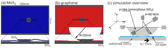
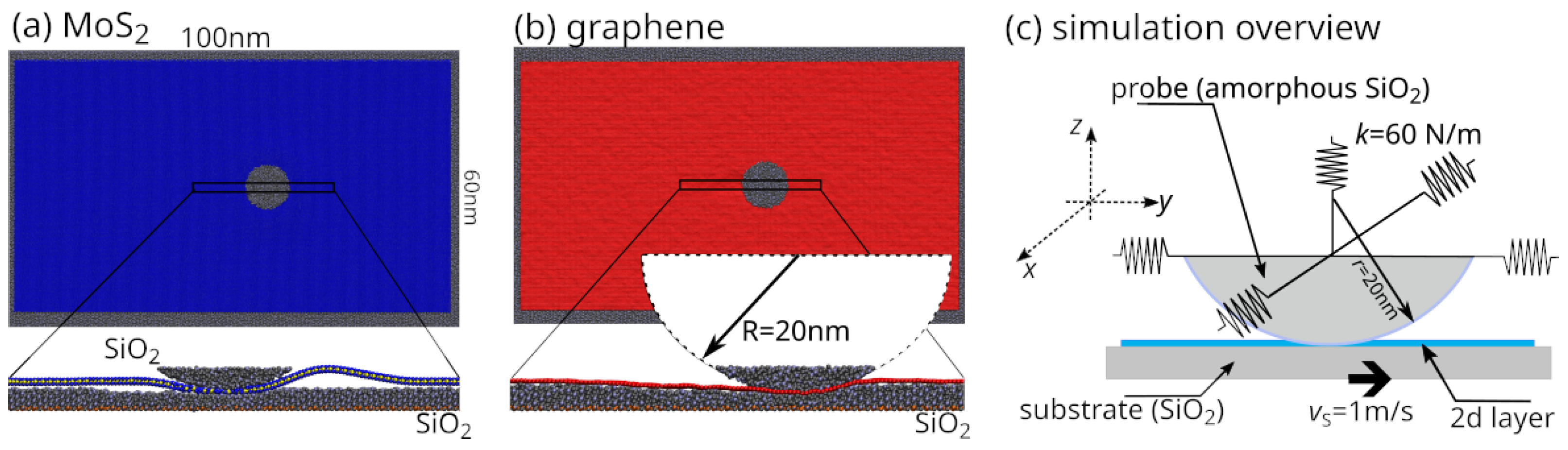
The simulated systems correspond to the geometries illustrated schematically in Figure 1. Two distinct configurations were considered, namely: (a) MoS2 sheet on SiO2 substrate and (b) graphene sheet on SiO2 substrate. The simulation cell dimensions were approximately: 100 nm in the sliding direction and 60 nm in the transverse in-plane direction. Periodic boundary conditions (PBCs) were applied only to the SiO2 substrate in the in-plane directions, while the 2D materials (graphene and MoS2) were modeled as finite flakes. This choice was made to avoid artificial interactions between deformation fields and their periodic images. In particular, in the case of MoS2, the formation of an out-of-plane pucker under the indenter would interact with its periodic replicas if fully periodic boundary conditions were imposed on the 2D layer, leading to non-physical constraints on deformation and stress redistribution.
Figure 1.
Configuration snapshots of atomistic models used in MD simulations: (a) MoS2 on SiO2 substrate and (b) graphene on SiO2 substrate. Simulation cell dimensions are approximately: 100 nm × 60 nm. The rigid spherical SiO2 indenter (representing the tip in AFM experiments) with an effective radius of nm is sliding over the substrate while normal load is simultaneously applied. (c) Schematic representation of the implemented simulation setup, which is designed following the experimental AFM setup shown in panels (a,b) of this figure. The values of the parameters defining the simulation setup are sliding velocity m/s and spring stiffness coefficient N/m, which is the same for the elastic springs attached to the probe in all three Cartesian directions.
The SiO2 substrate was modelled as a slab. Its bottom layers were connected to so-called ghost atoms acting as fixed centres around which atoms can move, via an 8 kN/m spring to suppress deformation under AFM tip pressure and act as a rigid bulk. In contrast, the upper layers were fully dynamic and allowed to deform in response to applied loads. We placed a single layer of MoS2 or graphene on top of the SiO2 substrate.
Mechanical loading was applied using a rigid spherical SiO2 indenter representing a nanoscale contact, with an effective radius of nm (check Figure 1). The indenter probe was positioned above the centre of the simulation cell. Such a geometry enabled a controlled investigation of stress distribution, interfacial shear, and wear processes in the 2D coatings. The graphene was studied at normal loads of 0.75 μN and 0.5 μN, while MoS2 was studied at normal loads of 0.65 μN and 0.5 μN. For our setup, 0.65 μN was the maximum load that MoS2 could sustain without immediately breaking. The 0.5 µN load was selected as a common reference condition for direct comparison between the two materials. The higher loads correspond to material-specific regimes approaching the onset of structural failure, and are therefore used to analyse rupture behaviour rather than for direct comparison.
The probe is connected to the support via harmonic elastic springs in all three orthogonal directions (x-, y-, and z-) to measure the lateral and normal forces, similar to a Friction Force Microscopy (FFM) experiment. The probe has a spring stiffness of N/m in all three orthogonal directions, cf. Figure 1c. The probe support is fixed while the SiO2 substrate (i.e., the ghost atoms) moves at a sliding velocity m/s (similar to AFM experiment). Normal loading was applied by displacing the rigid spherical indenter’s support vertically toward the coating on the substrate until the desired normal contact force was achieved. Subsequently, lateral sliding was imposed by prescribing a constant sliding velocity m/s to the ghost atoms along the in-plane direction, mimicking AFM-based scratching and wear experiments. The same “loading-plus-sliding” protocol was applied to both graphene and MoS2 systems to enable direct comparison of their deformation and wear behaviour under comparable mechanical conditions, with a direct comparison performed at a common normal load of 0.5 µN. Before sliding, the systems were relaxed by thermal equilibration at K to remove residual stresses. Temperature control was applied via a Nose–Hoover thermostat.
Atomic trajectories, forces, and energies were recorded during the MD simulations. Structural analysis focused on atomic displacements, coordination changes, bond rupture events, and local deformations of both 2D (MoS2/graphene) layers and SiO2 substrate. These analyses enabled the identification of distinct deformation and failure regimes, including elastic and plastic deformation, the onset of fracture, material removal, and exposure of the underlying substrate. Atomistic mechanisms observed in the simulations were instrumental in interpreting the differences in wear resistance and load-bearing behaviour between graphene and MoS2 coatings.
3. Results
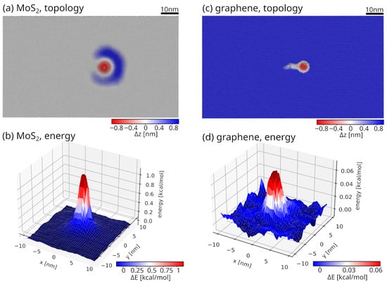
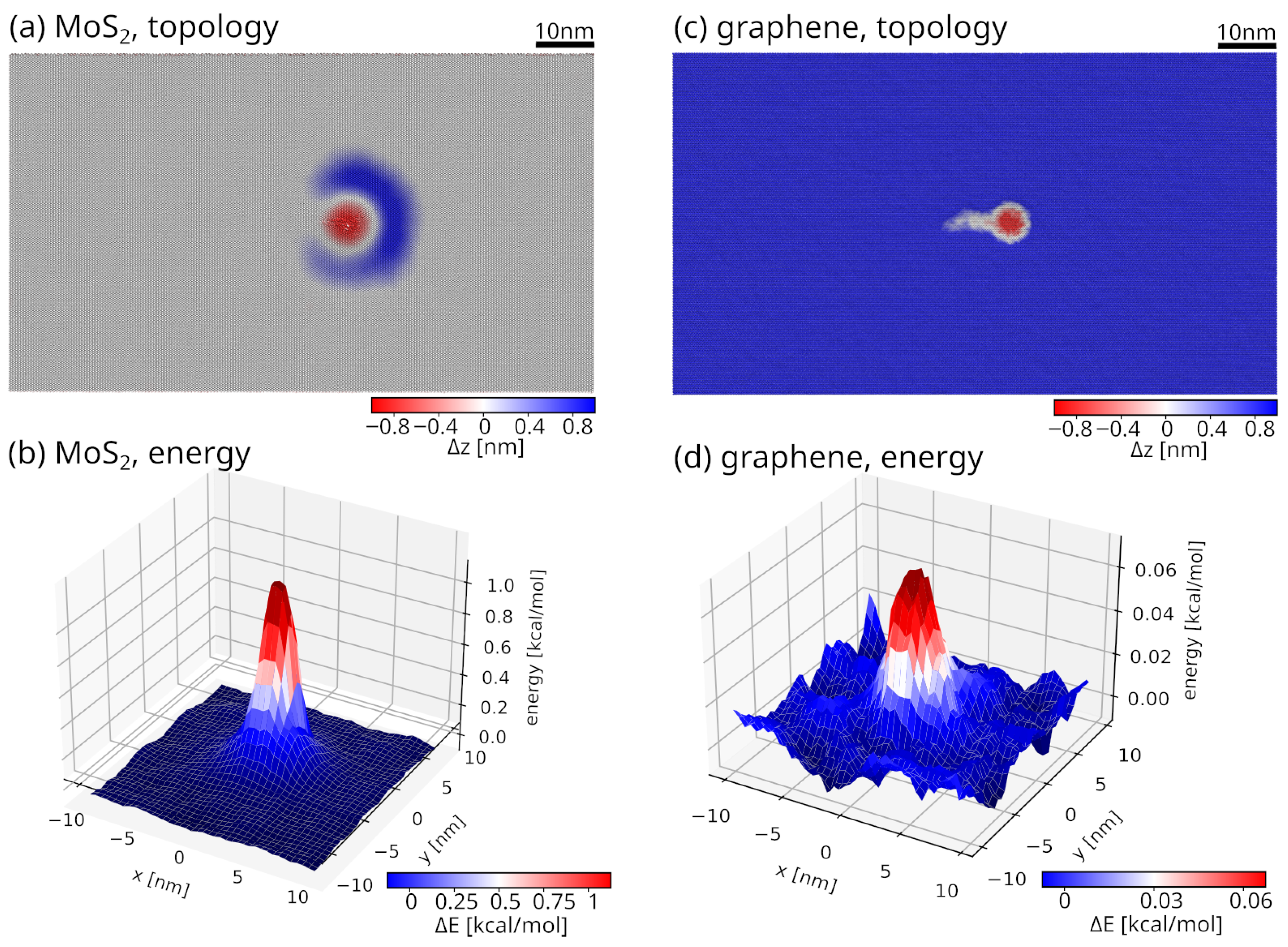
We have quantified the deformation of both MoS2 and graphene on SiO2 substrate under controlled and similar nanomechanical conditions, the results of which are shown in Figure 2. In the case of MoS2, cf. Figure 2a, the displacement results in the pronounced puckering beneath the contact with the indenter. This pucker extends laterally beyond the immediate region of contact with the tip, reflecting the layered MoS2 structure’s ability to accommodate mechanical load through out-of-plane bending and interlayer shear. The result presented in Figure 2b shows a strong localisation of the per-atom potential energy within the pucker region, with peak energy values nearly twenty times higher than those observed in graphene (shown in Figure 2d). This result demonstrates that MoS2 absorbs a significant fraction (i.e., 95%) of the applied mechanical energy through internal deformation, thereby absorbing the tip-induced disturbance and shielding the underlying SiO2 substrate from excessive stress.
Figure 2.
Spatial maps of vertical atomic displacements and per-atom potential energy in the vicinity of the indenter in the 2D layer induced by nanomechanical contact for: MoS2 and graphene on SiO2 substrate. Colour maps show the out-of-plane (i.e., along the z-direction) displacement field, with the scale indicated by the colour bars. MoS2 is a plane in the midpoint between forced down (red) and puckered material (blue). On the other hand, graphene does not form puckers, and blue atoms correspond to undeformed graphene. The per-atom energy localised in MoS2 is nearly twenty times that in graphene, indicating substantially stronger energy absorption and deformation within the MoS2 layer. The scale bar corresponds to 10 nm, as indicated in this figure.
In contrast, graphene, see Figure 2c, exhibits a much more localised deformation without extended puckering. The displacement field is confined to a narrow region around the contact point with the tip, and the per-atom energy accumulation remains comparatively low. Owing to its high in-plane stiffness and atomic thickness, graphene resists bending and stores less deformation energy, resulting in a more concentrated stress distribution at the interface. The in-plane stiffness (two-dimensional Young’s modulus, E) of monolayer graphene has been experimentally measured to be approximately 340 N/m using AFM nanoindentation techniques [54]. For monolayer MoS2, reported experimental value is 180 N/m [55]. For a comparison with three-dimensional (3D) materials, an effective Young’s modulus E can be obtained by dividing the 2D Young’s modulus by an effective layer thickness t. Using for graphene yields , while adopting for MoS2 gives –.
These observations highlight fundamentally different mechanisms for load accommodation in the two studied materials. MoS2 protects the substrate by puckering, absorbing, and redistributing deformation energy, whereas graphene responds primarily through localised elastic deflection, with limited energy storage within the coating.
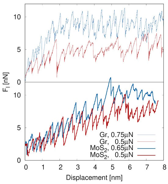
In the following, a direct comparison between graphene and MoS2 is performed at the common normal load of 0.5 µN. The higher-load cases are analysed separately to investigate material-specific responses near the onset of rupture in MoS2 and to observe a difference in graphene under sufficiently high loads. Figure 3 presents the lateral force as a function of sliding displacement for graphene and MoS2 coatings under different normal loads. In all cases, the lateral force exhibits a pronounced sawtooth-like behaviour characteristic of stick–slip motion at the scale of lattice constant (i.e., approximately 0.3 nm), reflecting the repeated cycles of pinning and consequent elastic loading of the probe spring, followed by sudden slip events at the 2D material interface.
Figure 3.
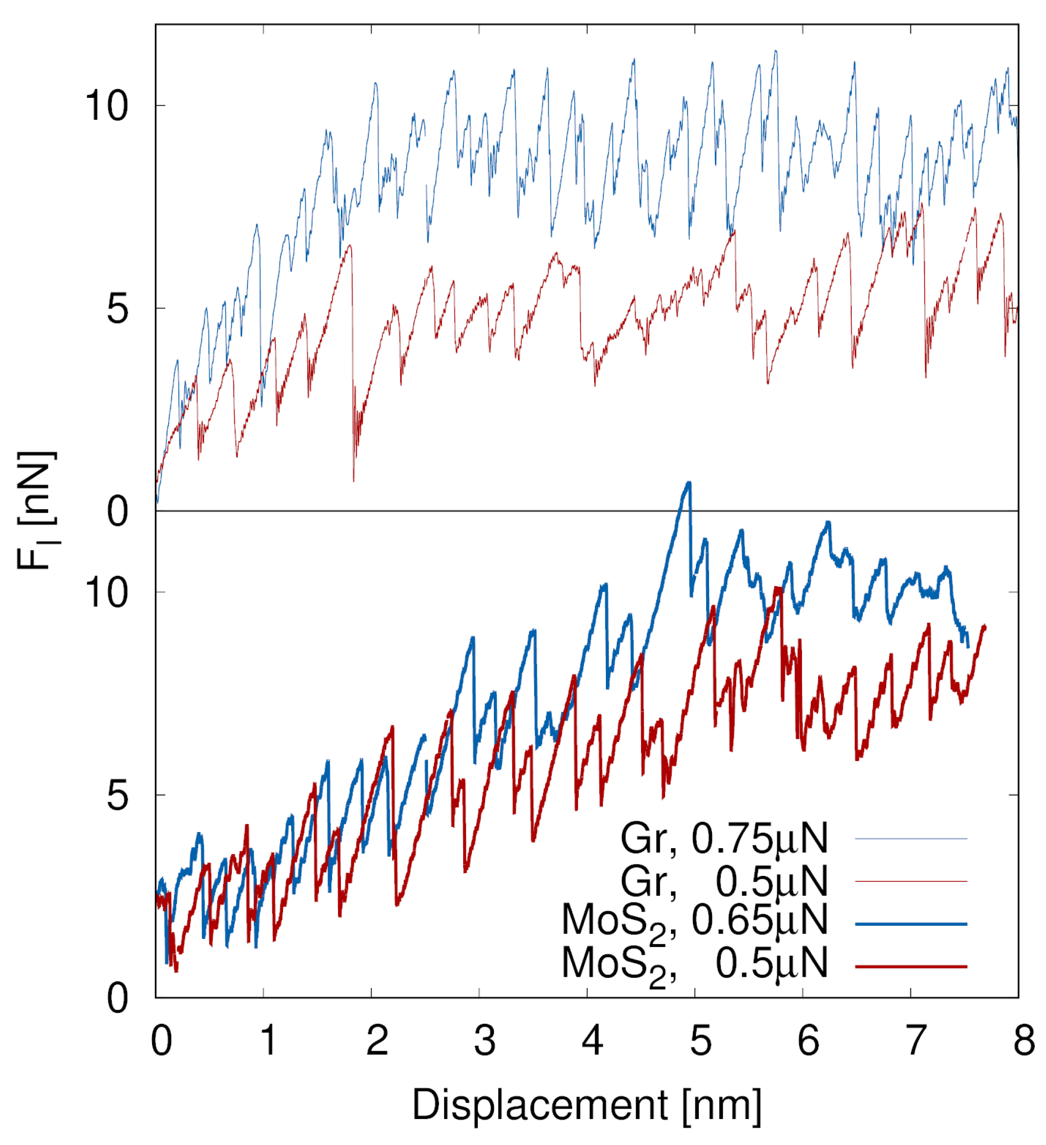
Lateral force as a function of sliding displacement for graphene (Gr) and MoS2 coatings under different normal loads. Upper panel: graphene at normal loads of 0.75 μN and 0.5 μN. Lower panel: MoS2 at normal loads of 0.65 μN and 0.5 μN. For our setup, 0.65 μN was the maximum load that MoS2 could sustain without immediately breaking. The sawtooth-like response of lateral force reflects the stick–slip motion during sliding. Since both graphene and molybdenum-disulfide have a crystal structure, observation of stick–slip friction is expected.
On slightly larger time and displacement scales, the graphene lateral force (shown in the upper panel of Figure 3) increases rapidly during the initial stage of sliding (up to 2 nm displacement) and reaches relatively high average values, particularly at the higher normal load of 0.75 μN. The initial upward trend in the mean value of suggests progressive modification of the contact and the formation of a lithographic track along the sliding path. This behaviour is consistent with localised deformation and limited energy dissipation within the graphene layer (as previously analysed; see Figure 2), leading to stress concentration in the SiO2 substrate as sliding proceeds. The amplitude of the stick–slip oscillations remains unaltered throughout the sliding, indicating the existence of sustained and simultaneous interfacial shear resistance as well as a separate mechanism of energy dissipation due to deformation of the SiO2 substrate.
In contrast, MoS2 exhibits more gradually increasing lateral forces (shown in the lower panel of Figure 3) up to a displacement of 5 nm, for comparable normal loads (i.e., matching of blue and red curves in the two panels of Figure 3). This behaviour suggests elastic energy accumulation in the MoS2 layer via deformation induced by the probe’s shear displacement. Such deformation mechanisms include puckering, as illustrated in Figure 1a and quantified in Figure 2a, as well as intralayer deformation. These mechanisms help to postpone the onset of significant interfacial damage. As a result, once the system reaches the yield stress, the MoS2 is slit apart, and the underlying substrate begins to deform plastically, though less than graphene under a similar normal load. Regarding stick–slip, we observe a difference between the two normal forces once the MoS2 layer ruptures. While for 0.5 µN the stick–slip sawtooth profile remains unaltered throughout sliding, at a higher load of 0.65 µN the sawtooth profile is increasingly smoother, due to an accumulating amount of damage in MoS2 as we will demonstrate later in this section.
The effective friction coefficient was estimated as the ratio of the mean lateral force and the applied normal load :
From Figure 3, we can estimate that the corresponding average lateral forces are higher, 7.6 ± 0.6 and 10.3 ± 0.7 nN for normal loads of 0.5 and 0.65 μN, respectively, in the case of MoS2, resulting in an effective friction coefficient of:
On the other hand, we can analogously estimate that graphene exhibits average lateral forces 6 ± 1.1 and 9 ± 1.3 nN for normal loads of and 0.75 μN, yielding an effective friction coefficient of:
From Figure 3, we can see that the elastic energy (estimated as ) stored in the MoS2-SiO2 system before the shear stress levels off is about three times larger than in the graphene-SiO2. Approximately, the values are 5 nm·7.6 nN ≈ 38 J in MoS2-SiO2 compared to 2 nm·6 nN ≈ 12 J for graphene-SiO2. In this way, MoS2 serves as a protective coating that absorbs energy from lateral deformation. Graphene exhibits a much more localised deformation response. Due to its atomic thickness and high in-plane stiffness, graphene resists out-of-plane bending and stores substantially less deformation energy at the contact. The absence of extended puckering is reflected in a per-atom elastic energy of graphene that is 20 times lower than in the case of MoS2, as presented in Figure 2b,d.
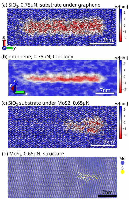
Figure 4 illustrates the formation and evolution of lithography tracks generated during nanoscale sliding contact. The tracks are visualised using both atomistic snapshots and coarse-grained representations, highlighting regions of enhanced plastic deformation and atom removal.
Figure 4.
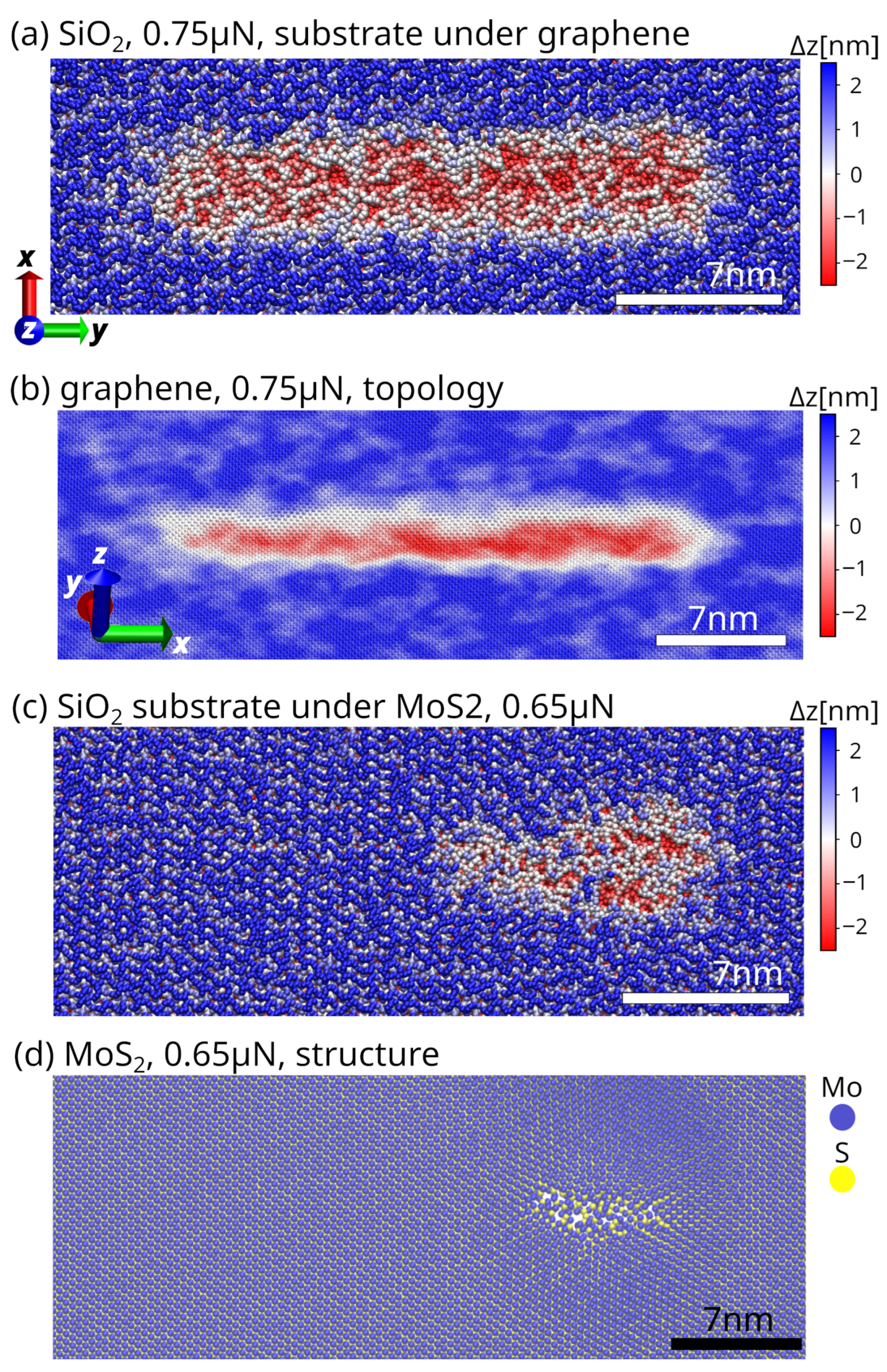
Configuration snapshots illustrating the formation and evolution of lithography tracks formed over the course of nanoscale sliding of the spherical SiO2 indenter. In all MD simulations, the sliding direction is along the longer y-axis. Panel (a): structure of the SiO2 substrate under graphene at the applied normal load of 0.75 μN in the initial stage of sliding. Panel (b): topology of graphene at the applied normal load of 0.75 μN in the initial stage of sliding. Panel (c): structure of the SiO2 substrate under MoS2 at the applied normal load of 0.65 μN at the end of the sliding path. Panel (d): structure of MoS2 at the applied normal load of 0.65 μN at the end of the sliding path.
In the initial stage of sliding, i.e., top panels of Figure 4 referring to (a) SiO2 substrate under graphene and (b) graphene, a continuous lithography track develops along the sliding direction. This track is characterised by an elongated band of high deformation and energy accumulation spanning several nanometers. The track width exceeds the immediate contact area, indicating that deformation is not confined to a single atomic row, but is redistributed laterally across the 2D layer and the underlying substrate.
The coarse-grained representation emphasises the spatial continuity of the lithography track, revealing a relatively uniform deformation band along the sliding path. This behaviour reflects repeated stick–slip events due to the sliding over the periodic structure of a 2D material, which progressively modifies the underlying substrate surface and accumulates deformation along the indenter’s sliding trajectory. The persistence of the track demonstrates that the material response is dominated by cumulative plastic deformation rather than isolated, reversible stick–slip elastic events, which are confined to the investigated 2D materials.
At the end of the sliding path on MoS2, cf. panel of Figure 4c, there is a compact damage zone. This zone is about 5–7 nm long in MoS2 and about 3 nm long in the SiO2 substrate. The damage region corresponds to the termination of the lithography track, where stresses concentrate, and the probe breaks into a MoS2 pucker. Such localisation is indicative of incipient irreversible 2D material deformation, i.e., fracture, material removal, or defect clustering, depending on the local stress state and material properties. The atomic-scale view of fractured MoS2 in Figure 4d reveals the microscopic consequence of the prolonged lithography track and accumulation of stress beyond the yield point in pucker, resulting in permanent damage.
In contrast to MoS2, in graphene local lattice distortions are observed within the track region, while the surrounding lattice remains largely intact, cf. Figure 2c and Figure 4b. The localisation of graphene deformation under the probe confirms that lithography is not inhibited by highly localised structure rearrangements and defect generation, confined to a narrow region defined by the sliding contact. Overall, configuration snapshots presented in Figure 4 demonstrate that the formation of lithography tracks is prevented by the accumulation of localised deformation in a 2D layer along the sliding path in the form of a pucker.
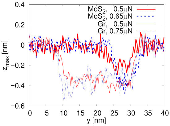
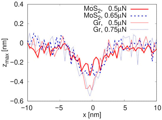
Formation and morphological characteristics of the lithography tracks in the SiO2 substrate depicted in Figure 4 are quantitatively investigated based on the longitudinal profiles of the track presented in Figure 5 for both MoS2 and graphene (Gr). Here, denotes the maximum out-of-plane coordinate (along the z direction) of SiO2 substrate atoms within a slice of width ±0.5 nm centered at position y. MoS2 exhibits a track shorter than the probe path (about 5 nm out of 25 nm) and approximately 0.19 nm deep the lower simulated normal load, i.e., 0.5 µN see Table 1. It appears only when the material is broken, following the rupture of a pucker beneath the contact as a consequence of the accumulation of lateral strain in the layer, as illustrated in Figure 1a. On the contrary, the profile for graphene reveals the development of a 22 nm long and 0.4 nm deep trace along the total length of the simulated contact between the probe and the 2D layer. At 0.65 µN normal load, after MoS2 is completely ripped apart, the track depth is similar in MoS2 and graphene. Figure 6 shows the cross-section profile of the track at nm (once the MoS2 layer is broken).
Figure 5.
Longitudinal profile of of the track in SiO2 substrate (i.e., along the sliding direction y) for MoS2 and graphene (Gr) under different normal loads. The quantity represents the maximum out-of-plane coordinate (along the z direction) of SiO2 substrate atoms within a slice of width ±0.5 nm centered at position y, evaluated at .
Table 1.
Summary of key quantities extracted from simulations. Mean lateral force is computed over the steady-state sliding regime after the initial transient, i.e., final 5 nm of the track for graphene and 2 nm for MoS2. The track depth is defined as the vertical distance from the reference level given by the z-coordinate of the topmost substrate atoms along the track. The track width and length are measured at half of this depth.
Figure 6.
Profile of a cut through lithographic track in SiO2 substrate for MoS2 and graphene (Gr) under different normal loads. The quantity represents the maximum out-of-plane coordinate (along the z direction) of SiO2 substrate atoms within a slice of width ±0.5 nm centered at position x, evaluated at nm.
4. Discussion
In this work, simulation parameters were selected to reproduce the essential contact geometry and loading protocol of AFM-based nanotribology experiments, while remaining compatible with atomistic MD time scales. Accordingly, the results are interpreted primarily in a mechanistic and comparative sense rather than as a direct one-to-one reproduction of experimental sliding rates. The present simulations rely on several modelling assumptions that should be considered when interpreting the results. While the sliding velocity (1 m/s) is higher than in typical AFM experiments (reflecting limitations of the standard molecular dynamics time scale), it is comparable to that in many technical friction systems. The indenter is modelled as a rigid SiO2 sphere, with probe deformation neglected. The 2D materials are represented as finite flakes rather than continuous layers to avoid artificial interactions of deformation fields, particularly MoS2 puckers, with their periodic images. Stability on the substrate is maintained solely through van der Waals adhesion, similar to that of single-layer nanoflakes of a solid lubricant. Results presented in the Section 3 reveal clear and fundamental differences in the mechanical response, frictional behaviour, as well as wear mechanisms of MoS2 and graphene under a nanoscale sliding contact with the SiO2 indenter. Although both materials belong to the class of two-dimensional crystals, their distinct out-of-plane responses to the applied load and sliding, along with different internal deformation pathways, lead to fundamentally different nanotribological behaviour. The central finding of this work is the manner in which mechanical energy is accommodated at the contact in the two studied 2D materials—MoS2 and graphene.
The per-atom energy distributions demonstrate that MoS2 concentrates nearly twenty times more deformation energy within the coating than graphene, cf. Figure 2. This energy localisation is accompanied by the pronounced puckering beneath the contact, as evidenced by both the displacement maps and the profiles. The pucker represents a stable out-of-plane deformation mode that allows MoS2 to absorb mechanical energy through bending and interlayer shear, thereby acting as an effective mechanical buffer. As a consequence, a significant fraction of the applied load is taken over by the MoS2 layer itself, thus reducing stress transmission to the underlying SiO2 substrate. This localised response and low elastic energy absorption result in higher stress concentrations beneath the graphene in SiO2, thereby promoting bond distortion and plastic deformation along the entire sliding path. Consequently, graphene accommodates the applied load, leaving a lithographic mark even when the probe is removed.
These substantial differences in deformation mechanisms directly manifest in the lateral force response under comparable normal loads. Both materials exhibit stick–slip motion, characteristic of nanoscale friction in crystalline materials; however, MoS2 consistently shows higher average lateral forces and larger stick–slip amplitudes than graphene, at similar normal loads. The rapid levelling off of the mean lateral force with sliding distance for graphene occurs within the first 2 nm. After the initial wear-in process, a 0.4 nm deep wear track is formed. It should be emphasised that direct quantitative comparisons between materials are restricted to the common load of 0.5 µN. At higher loads, the systems operate in different regimes relative to their mechanical stability limits, and the observed differences reflect intrinsic material-dependent failure mechanisms rather than equivalent loading conditions.
In contrast, the stronger dependence of lateral force on displacement for MoS2 reflects the gradual formation of a pucker and initially absent wear. Estimated effective friction coefficients further support this reasoning, with MoS2 showing higher friction than graphene, only saturating when a rupture point of MoS2 under the probe is reached.
The morphology of the lithography tracks provides additional insight into the wear mitigation processes. In MoS2, the lithography tracks are absent on the SiO2 substrate, consistent with pucker-mediated buffering and delayed severe wear, until the 2D sheet structure is ruptured. In graphene, however, the tracks are characterised by plastically deformed regions and lithographic deformation of the graphene sheet along the track. This behaviour is consistent with the strong localisation of deformation observed in both the out-of-plane displacement and per-atom potential energy analyses. Experimental studies on CVD-grown films have shown that under sufficiently high contact pressures, both graphene and MoS2 can undergo rapid removal, with MoS2 exhibiting layer-by-layer wear and graphene detaching early due to weaker interfacial bonding [14]. In contrast, the present simulations probe an intermediate loading regime, where graphene remains largely intact while MoS2 exhibits localised deformation and rupture, highlighting the load-dependent transition between distinct wear mechanisms. Furthermore, in MoS2, additional layers facilitate interlayer sliding, likely increasing resistance to rupture. While the present work focuses on monolayers to isolate fundamental mechanisms, extension to multilayer systems represents a natural and important direction for future study.
Importantly, the correlation between lithography tracks and out-of-plane deformation in 2D materials provides a unifying framework for understanding the nanoscale mechanism for wear prevention. 2D materials capable of forming extended out-of-plane deformation structures, such as puckers in MoS2, can effectively accommodate externally applied mechanical disturbances, thereby dissipating energy internally and protecting the underlying substrate. On the contrary, 2D materials with more rigid in-plane bonds, such as graphene, allow deformation and damage only along the sliding trajectory, marginally increasing the radius of an AFM probe or an asperity in the tribological system with dry lubricants such as graphite, leading to increased friction and more pronounced wear.
5. Conclusions
All-atom molecular dynamics simulations were used to compare nanoscale friction, lithography, and wear mechanisms in MoS2 and graphene under sliding contact. Despite both being two-dimensional materials, their tribological responses differ fundamentally due to their distinct deformation modes. Graphene, with its high in-plane stiffness, exhibits localised deformation and promotes stress concentration in the substrate, leading to plastic damage along the sliding path. In contrast, MoS2 accommodates the applied load through out-of-plane puckering, enabling effective energy dissipation, higher friction levels, and delayed wear while protecting the substrate.
These findings highlight the critical role of deformation mechanisms in governing nanoscale friction and wear. Materials capable of redistributing stresses through out-of-plane deformation are particularly effective for tribological applications. While the present results focus on monolayers, the underlying physical mechanisms are expected to remain relevant for multilayer systems, where interlayer effects may further influence the response.
Future work should aim to quantitatively compare friction, failure thresholds, and wear-track formation using matched AFM experiments.
Author Contributions
Conceptualisation, M.D. and I.S.; methodology, I.S.; formal analysis, I.S.; writing—original draft preparation, I.S.; writing—review and editing, M.D.; visualisation, I.S.; funding acquisition, I.S. and M.D. All authors have read and agreed to the published version of the manuscript.
Funding
The authors acknowledge funding provided by the Institute of Physics Belgrade, through the grant of the Ministry of Science, Technological Development and Innovation of the Republic of Serbia, the training and support received through the COST (European Cooperation in Science and Technology) Action MecaNano CA21121, and an internal project of Universidad Técnica Federico Santa María PA_INST_2025_23.
Data Availability Statement
The original contributions presented in this study are included in the article. Further inquiries can be directed to the corresponding author.
Acknowledgments
All computer simulations were performed on the PARADOX supercomputing facility at the Scientific Computing Laboratory of the Institute of Physics Belgrade, University of Belgrade, Serbia.
Conflicts of Interest
The authors declare no conflicts of interest.
References
- Vakis, A.; Yastrebov, V.; Scheibert, J.; Nicola, L.; Dini, D.; Minfray, C.; Almqvist, A.; Paggi, M.; Lee, S.; Limbert, G.; et al. Modeling and Simulation in Tribology across Scales: An Overview. Tribol. Int. 2018, 125, 169–199. [Google Scholar] [CrossRef] [Scilit]
- Stoyanov, P.; Chromik, R.R. Scaling Effects on Materials Tribology: From Macro to Micro Scale. Materials 2017, 10, 550. [Google Scholar] [CrossRef] [Scilit] [PubMed]
- Htwe, Y.Z.N.; Al-Janabi, A.S.; Wadzer, Y.; Mamat, H. Review of Tribological Properties of Nanoparticle-Based Lubricants and Their Hybrids and Composites. Friction 2024, 12, 569–590. [Google Scholar] [CrossRef] [Scilit]
- Bhushan, B.; Israelachvili, J.N.; Landman, U. Nanotribology: Friction, Wear and Lubrication at the Atomic Scale. Nature 1995, 374, 607–616. [Google Scholar] [CrossRef] [Scilit]
- Sadeghi, B.; Cavaliere, P.; Shabani, A.; Pruncu, C.I.; Lamberti, L. Nano-Scale Wear: A Critical Review on Its Measuring Methods and Parameters Affecting Nano-Tribology. Proc. Inst. Mech. Eng. Part J 2024, 238, 125–155. [Google Scholar] [CrossRef] [Scilit]
- Kurihara, K. Confined Liquids Studied by Resonance Shear Measurement: Molecular Mechanism of Lubrication. Langmuir 2025, 41, 6417–6428. [Google Scholar] [CrossRef] [Scilit]
- Di Lecce, S.; Kornyshev, A.A.; Urbakh, M.; Bresme, F. Structural Effects in Nanotribology of Nanoscale Films of Ionic Liquids Confined between Metallic Surfaces. Phys. Chem. Chem. Phys. 2021, 23, 22174–22183. [Google Scholar] [CrossRef] [Scilit]
- Dašić, M.; Stanković, I.; Gkagkas, K. Influence of Confinement on Flow and Lubrication Properties of a Salt Model Ionic Liquid Investigated with Molecular Dynamics. Eur. Phys. J. E 2018, 41, 130. [Google Scholar] [CrossRef] [Scilit]
- Berman, D.; Erdemir, A.; Sumant, A.V. Graphene: A New Emerging Lubricant. Mater. Today 2014, 17, 31–42. [Google Scholar] [CrossRef] [Scilit]
- Ge, X.; Chai, Z.; Shi, Q.; Liu, Y.; Wang, W. Graphene Superlubricity: A Review. Friction 2023, 11, 1953–1973. [Google Scholar] [CrossRef] [Scilit]
- Ab Rahman, M.; Thien, G.S.H.; Shahid, M.; Ling, T.Y.; Hashem, A.; Chan, K.Y.; Johan, M.R. Graphene as a Lubricant Additive for Reducing Friction and Wear in Its Liquid-Based Form. Lubricants 2023, 11, 29. [Google Scholar] [CrossRef] [Scilit]
- Almonti, D.; Baiocco, G.; Menna, E.; Rubino, G. Enhanced wear resistance in Nickel-graphene-PTFE composite coatings: Fabrication and characterisation. Surf. Eng. 2025, 41, 383–392. [Google Scholar] [CrossRef] [Scilit]
- Vazirisereshk, M.R.; Martini, A.; Strubbe, D.A.; Baykara, M.Z. Solid Lubrication with MoS2: A Review. Lubricants 2019, 7, 57. [Google Scholar] [CrossRef] [Scilit]
- Cho, D.H.; Jung, J.; Kim, C.; Lee, J.; Oh, S.D.; Kim, K.S.; Lee, C. Comparison of Frictional Properties of CVD-Grown MoS2 and Graphene Films under Dry Sliding Conditions. Nanomaterials 2019, 9, 293. [Google Scholar] [CrossRef] [Scilit]
- Mukhtar, S.H.; Gulzar, A.; Saleem, S.; Wani, M.; Sehgal, R.; Yakovenko, A.; Goryacheva, I.; Sharma, M.D. Advances in Development of Solid Lubricating MoS2 Coatings for Space Applications. Tribol. Int. 2024, 192, 109194. [Google Scholar] [CrossRef] [Scilit]
- Xiong, L.; Wu, M.; Fan, X.; Zhu, M. Study on the Preparation and Fretting Behavior of Bonded Oriented MoS2 Solid Lubricant Coating. Friction 2024, 12, 2505–2518. [Google Scholar] [CrossRef] [Scilit]
- Huynh, N.P.; Kim, H.J.; Chung, K.H. Long-term wear characteristics of single-layer h-BN, MoS2, and graphene. Tribol. Int. 2026, 213, 111059. [Google Scholar] [CrossRef] [Scilit]
- Akinwande, D.; Brennan, C.J.; Bunch, J.S.; Egberts, P.; Felts, J.R.; Gao, H.; Huang, R.; Kim, J.S.; Li, T.; Li, Y.; et al. A review on mechanics and mechanical properties of 2D materials—Graphene and beyond. Extrem. Mech. Lett. 2017, 13, 42–77. [Google Scholar] [CrossRef] [Scilit]
- Tomanik, E.; Christinelli, W.; Souza, R.M.; Oliveira, V.L.; Ferreira, F.; Zhmud, B. Review of Graphene-Based Materials for Tribological Engineering Applications. Eng 2023, 4, 2764–2811. [Google Scholar] [CrossRef] [Scilit]
- Wang, G.; Dai, Z.; Xiao, J.; Feng, S.; Weng, C.; Liu, L.; Xu, Z.; Huang, R.; Zhang, Z. Bending of Multilayer van der Waals Materials. Phys. Rev. Lett. 2019, 123, 116101. [Google Scholar] [CrossRef] [Scilit]
- Ran, D.; Yuan, Z.; Du, P.; Wang, N.; Wang, N.; Zhao, L.; Feng, S.; Jia, W.; Wu, C. Multiscale Investigation of the Anti-Friction Mechanism in Graphene Coatings on Copper Substrates: Substrate Reinforcement via Microstructural Evolution. Lubricants 2025, 13, 457. [Google Scholar] [CrossRef] [Scilit]
- Zhao, S.; Zhang, Z.; Wu, Z.; Liu, K.; Zheng, Q.; Ma, M. The Impacts of Adhesion on the Wear Property of Graphene. Adv. Mater. Interfaces 2019, 6, 1900721. [Google Scholar] [CrossRef] [Scilit]
- Klemenz, A.; Pastewka, L.; Balakrishna, S.G.; Caron, A.; Bennewitz, R.; Moseler, M. Atomic Scale Mechanisms of Friction Reduction and Wear Protection by Graphene. Nano Lett. 2014, 14, 7145–7152. [Google Scholar] [CrossRef] [Scilit]
- Vasić, B.; Matković, A.; Gajić, R.; Stanković, I. Wear properties of graphene edges probed by atomic force microscopy based lateral manipulation. Carbon 2016, 107, 723–732. [Google Scholar] [CrossRef] [Scilit]
- He, Y.; Geng, Y.; Yan, Y.; Luo, X. Fabrication of Nanoscale Pits with High Throughput on Polymer Thin Film Using AFM Tip-Based Dynamic Plowing Lithography. Nanoscale Res. Lett. 2017, 12, 544. [Google Scholar] [CrossRef] [Scilit]
- Liu, Z.; Szczefanowicz, B.; Lopes, J.M.J.; Gan, Z.; George, A.; Turchanin, A.; Bennewitz, R. Nanoscale Friction on MoS2/Graphene Heterostructures. Nanoscale 2023, 15, 5809–5815. [Google Scholar] [CrossRef] [Scilit]
- Zambudio, A.; López-Polín, G.; Ares, P.; Colchero, J.; Gómez-Herrero, J.; Gómez-Navarro, C. High Frictional Resilience of MoS2 Nanosheets to Induced Atomic Vacancies: Implications for Nanoelectromechanical Devices. ACS Appl. Nano Mater. 2024, 7, 9712–9719. [Google Scholar] [CrossRef] [Scilit]
- Pešić, J.; Leitner, S.; Neilson, J.; Stanković, I.; Khan, M.Z.; Tizić Matković, D.; Kelly, A.G.; Carey, T.; Coleman, J.; Matković, A. Imaging junctions in two-dimensional semiconductor nanosheet networks. npj 2D Mater. Appl. 2025, 9, 90. [Google Scholar] [CrossRef] [Scilit]
- Sun, Y.; Wang, Y.; Wang, E.; Wang, B.; Zhao, H.; Zeng, Y.; Zhang, Q.; Wu, Y.; Gu, L.; Li, X.; et al. Determining the Interlayer Shearing in Twisted Bilayer MoS2 by Nanoindentation. Nat. Commun. 2022, 13, 3898. [Google Scholar] [CrossRef] [Scilit]
- Zaidi, H.; Richard, C.; Bui, H.S.; Tournis, S.; Aissa, M.; Bouguerra, K. Frictional Behavior of MoS2 Coatings: A Comparative Study of Dynamic and Static Friction in Vacuum and Inert Gases. Coatings 2025, 15, 500. [Google Scholar] [CrossRef] [Scilit]
- Barri, N.; Rastogi, A.; Islam, M.A.; Kumral, B.; Demingos, P.G.; Onodera, M.; Machida, T.; Singh, C.V.; Filleter, T. Cyclic Wear Reliability of 2D Monolayers. ACS Appl. Mater. Interfaces 2024, 16, 27979–27987. [Google Scholar] [CrossRef] [Scilit]
- Zhang, D.; Li, Z.; Klausen, L.H.; Li, Q.; Dong, M. Friction Behaviors of Two-Dimensional Materials at the Nanoscale. Mater. Today Phys. 2022, 27, 100771. [Google Scholar] [CrossRef] [Scilit]
- Fan, X.; He, C.; Ding, J.; Gao, Q.; Ma, H.; Lemme, M.C.; Zhang, W. Graphene MEMS and NEMS. Microsyst. Nanoeng. 2024, 10, 154. [Google Scholar] [CrossRef] [Scilit] [PubMed]
- Liu, Z.; Zhu, L.; Yuan, S.; Zhang, Y.; Zhang, P.; Cai, Z.; Liu, L.; Yang, R. Functional 2D MoS2 NEMS Resonator Array with Independent Electronic Tunability Based on Mass Transfer Printing. Microsyst. Nanoeng. 2026, 12, 21. [Google Scholar] [CrossRef] [Scilit]
- Rodríguez, S.J.; Candia, A.E.; Stanković, I.; Passeggi, M.C., Jr.; Ruano, G.D. Study of In-Plane and Interlayer Interactions During Aluminum Fluoride Intercalation in Graphite: Implications for the Development of Rechargeable Batteries. ACS Appl. Nano Mater. 2023, 6, 16977–16985. [Google Scholar] [CrossRef] [Scilit]
- Dašić, M.; Almog, R.; Agmon, L.; Yehezkel, S.; Halfin, T.; Jopp, J.; Ya’akobovitz, A.; Berkovich, R.; Stanković, I. Role of Trapped Molecules at Sliding Contacts in Lattice-Resolved Friction. ACS Appl. Mater. Interfaces 2024, 16, 44249–44260. [Google Scholar] [CrossRef] [Scilit]
- Plimpton, S. Fast Parallel Algorithms for Short-Range Molecular Dynamics. J. Comput. Phys. 1995, 117, 1–19. [Google Scholar] [CrossRef] [Scilit]
- Thompson, A.P.; Aktulga, H.M.; Berger, R.; Bolintineanu, D.S.; Brown, W.M.; Crozier, P.S.; in ’t Veld, P.J.; Kohlmeyer, A.; Moore, S.G.; Nguyen, T.D.; et al. LAMMPS—A Flexible Simulation Tool for Particle-Based Materials Modeling at the Atomic, Meso, and Continuum Scales. Comput. Phys. Commun. 2022, 271, 108171. [Google Scholar] [CrossRef] [Scilit]
- Karplus, M.; McCammon, J.A. Molecular Dynamics Simulations of Biomolecules. Nat. Struct. Biol. 2002, 9, 646–652. [Google Scholar] [CrossRef] [Scilit]
- Stankovic, I.; Hess, S.; Kröger, M. Microscopic structure, dynamics, and wear at metal-metal interfaces in sliding contact. Phys. Rev. E 2004, 70, 066139. [Google Scholar] [CrossRef] [Scilit] [PubMed]
- Stankovic, I.; Hess, S.; Kröger, M. Structural changes and viscoplastic behavior of a generic embedded-atom model metal in steady shear flow. Phys. Rev. E 2004, 69, 021509. [Google Scholar] [CrossRef] [Scilit]
- Kröger, M.; Stankovic, I.; Hess, S. Towards Multiscale Modeling of Metals via Embedded Particle Computer Simulation. Multiscale Model. Simul. 2003, 1, 25–39. [Google Scholar] [CrossRef] [Scilit]
- Zhou, J.; Lu, Y.; Wang, C.; Feng, D.; Zhang, H.; Li, Y. Molecular Dynamics Study of Graphene-Coated Reinforced Tribomechanical Properties: Hard versus Soft Substrates. Comput. Mater. Sci. 2023, 226, 112209. [Google Scholar] [CrossRef] [Scilit]
- Hu, C.; Yi, C.; Bai, M.; Lv, J.; Tang, D. Molecular Dynamics Study of the Frictional Properties of Multilayer MoS2. RSC Adv. 2020, 10, 17418–17426. [Google Scholar] [CrossRef] [Scilit] [PubMed]
- Stanković, I.; Dašić, M.; Jovanović, M.; Martini, A. Effects of Water Content on the Transport and Thermodynamic Properties of Phosphonium Ionic Liquids. Langmuir 2024, 40, 9049–9058. [Google Scholar] [CrossRef] [Scilit]
- Acikgoz, O.; Baykara, M.Z. Speed Dependence of Friction on Single-Layer and Bulk MoS2 Measured by Atomic Force Microscopy. Appl. Phys. Lett. 2020, 116, 071603. [Google Scholar] [CrossRef] [Scilit]
- Vazirisereshk, M.R.; Ye, H.; Ye, Z.; Otero-de-la Roza, A.; Zhao, M.Q.; Gao, Z.; Johnson, A.T.C.; Johnson, E.R.; Carpick, R.W.; Martini, A. Origin of Nanoscale Friction Contrast between Supported Graphene, MoS2, and a Graphene/MoS2 Heterostructure. Nano Lett. 2019, 19, 5496–5505. [Google Scholar] [CrossRef] [Scilit]
- Vasić, B.; Stanković, I.; Matković, A.; Kratzer, M.; Ganser, C.; Gajić, R.; Teichert, C. Molecules on rails: Friction anisotropy and preferential sliding directions of organic nanocrystallites on two-dimensional materials. Nanoscale 2018, 10, 18835–18845. [Google Scholar] [CrossRef] [Scilit]
- Tersoff, J. New empirical approach for the structure and energy of covalent systems. Phys. Rev. B 1988, 37, 6991–7000. [Google Scholar] [CrossRef] [Scilit]
- Tersoff, J. Modeling solid-state chemistry: Interatomic potentials for multicomponent systems. Phys. Rev. B 1989, 39, 5566–5568. [Google Scholar] [CrossRef] [Scilit]
- Stewart, J.A.; Spearot, D.E. Atomistic simulations of nanoindentation on the basal plane of crystalline molybdenum disulfide (MoS2). Model. Simul. Mater. Sci. Eng. 2013, 21, 045003. [Google Scholar] [CrossRef] [Scilit]
- Sresht, V.; Govind Rajan, A.; Bordes, E.; Strano, M.S.; Pádua, A.A.; Blankschtein, D. Quantitative Modeling of MoS2–Solvent Interfaces: Predicting Contact Angles and Exfoliation Performance using Molecular Dynamics. J. Phys. Chem. C 2017, 121, 9022–9031. [Google Scholar] [CrossRef] [Scilit]
- Allen, M.P.; Tildesley, D.J. Computer Simulation of Liquids; Oxford University Press: Oxford, UK, 2017. [Google Scholar]
- Lee, C.; Wei, X.; Kysar, J.W.; Hone, J. Measurement of the Elastic Properties and Intrinsic Strength of Monolayer Graphene. Science 2008, 321, 385–388. [Google Scholar] [CrossRef] [Scilit] [PubMed]
- Bertolazzi, S.; Brivio, J.; Kis, A. Stretching and Breaking of Ultrathin MoS2. ACS Nano 2011, 5, 9703–9709. [Google Scholar] [CrossRef] [Scilit] [PubMed]

Disclaimer/Publisher’s Note: The statements, opinions and data contained in all publications are solely those of the individual author(s) and contributor(s) and not of MDPI and/or the editor(s). MDPI and/or the editor(s) disclaim responsibility for any injury to people or property resulting from any ideas, methods, instructions or products referred to in the content. |
© 2026 by the authors. Licensee MDPI, Basel, Switzerland. This article is an open access article distributed under the terms and conditions of the Creative Commons Attribution (CC BY) license.