


Highlights
- UV photochemical treatment removes residual carbon and suppresses defects in sol–gel Y2O3 films.
- UV-pretreated Y2O3 buffer films show fine grains, low roughness, and strong biaxial texture.
- Single-layer Y2O3 buffer replicates the Ni-W texture and enables epitaxial YBCO growth.
- YBCO films on the photochemical Y2O3 buffer reach a self-field Jc of 2.65 MA/cm2 at 77 K.
- A vacuum-free photochemical sol–gel route lowers the cost of YBCO-coated conductors.
What are the main findings?
- Photochemical treatment decomposes organic groups and removes residual carbon in sol–gel Y2O3 precursor films, suppressing volatilization-induced defects.
- The UV-pretreated Y2O3 buffer film is dense and crack-free with fine grains and good in-plane biaxial texture (FWHM 1.6–1.9°).
- Epitaxial YBCO grown on this single-layer buffer exhibits a self-field Jc of 2.65 MA/cm2 at 77 K with typical flux-pinning behavior.
What are the implications of the main findings?
- The findings reveal that a vacuum-free, photochemical-assisted sol–gel route is capable of fabricating high-quality single-layer Y2O3 buffer films on biaxially textured Ni–W tapes, which avoids complicated multi-stacked buffer strucutres and vacuum deposition techniques.
- This strategy simplifies the manufacturing workflow and cuts the production cost of YBCO-coated conductors, which is beneficial for their large-scale and low-cost practical applications.
- The underlying photochemical mechanism, namely low-temperature decomposition of organics species and efficient elimination of residual carbon, can be extended to other oxide buffers layers and solution-processed functional thin-film systems.
Abstract
Buffer layers are indispensable components for YBa2Cu3O7−δ(YBCO)-coated conductors deposited on biaxially textured Ni-W metallic substrates, which act as diffusion barrier and epitaxial growth templates for superconducting films. In this work, both the Y2O3 single buffer film and the subsequent YBCO superconductor film were successfully fabricated on cube-textured Ni-W tapes via a facile photochemical-assisted sol–gel method. Specifically, the precursor gel films of Y2O3 were pretreated by ultraviolet (UV) irradiation. High-energy UV photons break organic chemical bonds and generate ozone and active oxygen radicals, which effectively decompose organic components and eliminate residual carbon at a low temperature. This photochemical treatment suppresses pore defects caused by the violent volatilization of organic substances during high-temperature annealing. The UV-treated Y2O3 buffer films present fine uniform grains and a low surface roughness of 5.46 nm, possessing excellent biaxial texture. The single-layer Y2O3 buffer can perfectly inherit the texture characteristics of the Ni-W substrate and provide a high-quality epitaxial growth template. On this sol–gel-derived Y2O3 buffer layer, the sol–gel-prepared YBCO superconducting film achieves high-quality in-plane epitaxial growth. The optimized YBCO-coated conductor exhibits a self-field critical current density of 2.65 MA/cm2 at 77 K with a superconducting transition width of 2.0 K, which confirms excellent superconducting performance. This vacuum-free photochemical-assisted sol–gel strategy provides a low-cost and promising technical route for the fabrication of high-quality single-buffer-layer YBCO-coated conductors.
Keywords:
sol–gel; UV irradiation; photochemical; buffer film; YBCO superconductor; Y2O3 film; Ni-W tape 1. Introduction
The development of second-generation higher-temperature superconductors (HTSs) has attracted considerable attention owing to their high critical temperature, high current density, and compact dimensions, which endow them with great potential for power-engineering, medical and nuclear-physics applications [1,2,3]. Among these HTS materials, YBa2Cu3O7−δ (YBCO) is a promising candidate for power-engineering applications [4,5,6]. Over the past few years, extensive research efforts have been devoted to the fabrication of YBCO film conductors by different methods [7,8,9]. Among these preparation methods, the sol–gel method is simple, reliable, and feasible for engineering-scale implementation. The fabrication of engineering-scale superconducting tapes requires rolling-assisted biaxially textured (RABiTS) Ni-W metallic substrates, onto which superconducting materials are deposited. However, YBCO cannot be directly deposited on Ni-W substrates for two reasons. First, the sol–gel process involves subsequent high-temperature heat treatment. During this process, metallic elements readily diffuse into the superconducting film and degrade its superconducting performance. Second, grains in Ni-W tapes possess a well-defined crystallographic texture. Serving as a template, the substrate induces epitaxial growth of YBCO with grain misorientation angles below 10°, so as to achieve optimal electrical-conductivity performance.
Therefore, an intermediate buffer film is required between the superconducting film and the Ni-W substrate. This buffer film serves two functions: first, it acts as a diffusion barrier film; second, it functions as a template to induce epitaxial growth of the superconducting film on its surface, thereby assuring that the grain-boundary misorientation of YBCO remains below about 10°. The buffer films must possess lattice parameters well-matched with both the metal Ni-W substrate and YBCO. Over the past decade, numerous suitable materials including CeO2, Y2O3, BaZrO3, yttria-stabilized zirconia (YSZ) and La2Zr2O7 have been reported for buffer-film applications [10,11,12,13]. In these studies, the typical design adopts multi-stacked oxide buffer films, such as CeO2/YSZ/CeO2 or CeO2/YSZ/Y2O3 [14,15]. Nevertheless, fabricating such multi-stacked buffer structures increases manufacturing costs and complicates the preparation procedure. Moreover, the epitaxial quality of the buffer films can deteriorate with increasing thickness, because buffer materials exhibit lattice-constant mismatches relative to the metallic substrate [16]. Accordingly, it is desirable to develop a single-film buffer film. Y2O3, as a promising buffer-film candidate, has drawn considerable attention [17]. It adopts a bixbyite crystal structure with a lattice parameter of 10.607 Å and Y-Y atomic spacing of 3.75 Å. The small lattice mismatch enables epitaxial growth of YBCO on the Y2O3 buffer film. Meanwhile, Y2O3 exhibits favorable chemical compatibility with the Ni-W substrate. To date, Y2O3 buffer films have been deposited on Ni-W tapes by various vacuum-based techniques [18,19]. However, the high cost and complexity of vacuum-deposition technologies restrict the fabrication of long-length HTS tapes. Sol–gel technique has been adopted for buffer-film preparation, as it is a low-cost, straightforward approach requiring no vacuum equipment. Furthermore, sol–gel method allows precise compositional control of final products and the manufacture of long-length tapes. Hence, sol–gel method is considered one of the promising routes for producing low-cost coated conductors. Generally, sol–gel method requires high-temperature treatment to decompose precursor gel films. During thermal processing, volatilization of organic species from the gel film generates porous defects, which impair the epitaxial growth of buffer films. To obtain dense buffer films and reduce the heat treatment temperature, this work employs a photochemical approach combined with UV irradiation to prepare Y2O3 buffer films. Photochemical treatment of sol–gel precursors can effectively decompose organic functional groups, lower the crystallization temperature of films, and suppress inter-diffusion of metallic elements into buffer films [20,21,22]. The as-prepared Y2O3 buffer films exhibit epitaxial grains, dense microstructure, uniform grain size and fine grains. More importantly, the photochemical method can substantially lower the grain-growth temperature of Y2O3 [23,24,25], thereby preventing metal-element diffusion into the buffer film. YBCO superconducting films grow with preferred orientation on the buffer layer of single-sided Ni-W tapes. The resulting YBCO/Y2O3/Ni-W architecture demonstrates favorable superconducting performance.
2. Materials and Methods
The Y2O3 precursor solution was prepared using yttrium acetate as the raw material, and a mixture of methanol and lactic acid was adopted as the solvent. The molar ratio of methanol to lactic acid was 5:1. Lactic acid acts as a chelating agent to improve the stability of the sol and inhibit the rapid hydrolysis of the precursor. Yttrium acetate was dissolved in the mixed solvent and stirred at 70 °C for 2 h to obtain a transparent homogeneous solution, after the sol is formed, it is aged at room temperature for 24 h to achieve sufficient homogenization. The concentration of Y3+ ion was fixed at 1 mol/L. The Ni-W alloy tapes (Evico GmbH, Dresden, Germany) were used as the substrate. Before sol coating, the tapes were ultrasonically cleaned with absolute ethanol to remove surface organic contaminants and subsequently heat-treated at 900 °C for 1 h in a mixed N2 and H2 atmosphere (N2 95 vol%, H2 5 vol%) to eliminate surface oxide films. Y2O3 gel films were deposited via the dip-coating method with a withdrawal speed of 3 mm/s. To make the experiment closer to industrial production, the gel film was coated only on one side of the Ni-W substrate, while the other side was wiped off. The as-coated Y2O3 precursor films were first dried at 50 °C for 30 min to evaporate the organic solvent, this temperatures can suppress evaporation induced by vigorous boiling, which otherwise causes bubbles, pinholes and cracks in the gel film, and then photochemically treated under ultraviolet (UV) light (Model L2002A3, Ossila Ltd., Sheffield, UK. 185 nm: 10%, 254 nm: 90%) for 1 h. To increase the film thickness, the dip-coating, drying and UV irradiation procedures were repeated three times. Finally, the multilayer Y2O3 gel films were annealed at 700, 800 and 900 °C for 2 h in a humidified N2-H2 mixed atmosphere (N2 95 vol%, H2 5 vol%) with a heating rate of 10 °C/min.
The YBCO precursor solution was prepared using yttrium acetate, barium acetate, copper acetate as raw materials, with methanol serving as the primary solvent [26,27]. Yttrium acetate was dissolved in a mixed solution of methanol and diethylenetriamine at a mole ratio 1:1. Barium acetate was dissolved in a methanol–lactic acid mixture, where the mole ratio of Ba2+ to lactic acid was 1:2. Copper acetate was dissolved in methanol and acrylic acid with a Cu-to-acrylic acid mole ratio of 1:3. The three individual solutions were thoroughly mixed to form the homogeneous YBCO precursor solution, with a total metal ion concentration of 2 mol/L. YBCO gel films were deposited on the Y2O3-buffered Ni-W tapes by dip-coating at a withdrawal speed of 2 mm/s. The obtained gel films were pyrolyzed at 450 °C for 1 h in humidified oxygen, and subsequently annealed at 780 °C for 2 h in a humidified O2-N2 mixed atmosphere (O2 80 vol%, N2 20 vol%), the final YBCO film obtained has dimensions of 20 mm in length, 10 mm in width and 0.68 μm in thickness.
The phase composition and crystallographic orientation of Y2O3 buffer film were characterized by X-ray diffraction (XRD: Bruker AXS SE, Karlsruhe, Germany). The in-plane texture of Y2O3 and YBCO film was characterized by XRD Phi scan (Rigaku Corporation, Akishima, Japan). The surface morphologies of Y2O3 buffer film and YBCO superconducting film were observed using a field-emission scanning electron microscope (FE-SEM, JEOL Ltd., Akishima, Japan, JEOL-6700F). The surface roughness of the Y2O3 film was characterized by atomic force microscopy (AFM: Bruker Corporation, Billerica, MA, USA). The magnetic properties of the YBCO films were measured by a multi-function vibrating sample magnetometer (VersaLab-VSM: Quantum Design, Inc, San Diego, CA, USA). Fourier transform infrared (FT-IR) spectroscopy (Bruker AXS SE, Karlsruhe, Germany, VERTEX70) was employed to characterize functional group structures of precursor films. The four-probe (Quantum Design, Inc., San Diego, CA, USA) method was adopted to characterize the Jc and resistance–temperature (R-T) curves of YBCO-coated conductors.
3. Results
3.1. XRD Analysis
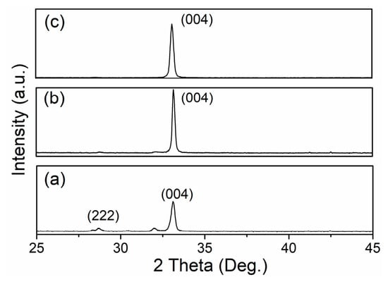
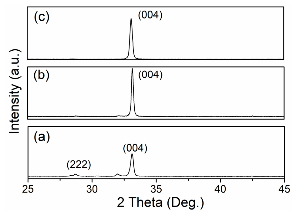
The Y2O3 precursor film was deposited on a cube-textured Ni-W metal substrate. After drying at 50 °C, the film was subjected to UV irradiation (wavelength of 185 nm (10%) and 254 nm (90%)) for 1 h. It was subsequently heat-treated at 700 °C, 800 °C and 900 °C for 2 h, respectively. The XRD patterns of the resulting films are shown in Figure 1. After heat treatment at 700 °C, the desired dominant (400) peak emerged, accompanied by the impurity (222) peak. When the annealing temperature was increased to 800 °C, a remarkable reduction in the intensity of the impurity (222) peak is observed, and the main (400) peak remained. After annealing at 900 °C, the film exhibited a single (400) diffraction peak. However, the full width at half-maximum (FWHM) of the Y2O3 film annealed at 900 °C was larger than that of the sample treated at 800 °C. This suggests that relatively coarse Y2O3 grains were formed upon annealing at 800 °C. According to the Arrhenius law [28], the atomic diffusion coefficient increases exponentially with temperature. Therefore, Y and O atoms have higher mobility at 900 °C, which normally promotes grain growth. Nevertheless, the cube-textured Ni-W substrate acts as an epitaxial template and provides abundant nucleation sites at elevated temperatures. The enhanced nucleation rate outweighs the grain-growth process. Consequently, fine grains with strong (400) preferred orientation are obtained at 900 °C.
Figure 1.
XRD of Y2O3 films annealed at different temperatures: (a) 700 °C, (b) 800 °C, and (c) 900 °C.
3.2. Microstructural Analysis
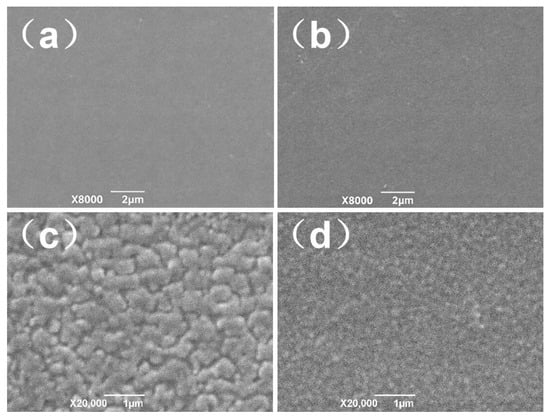
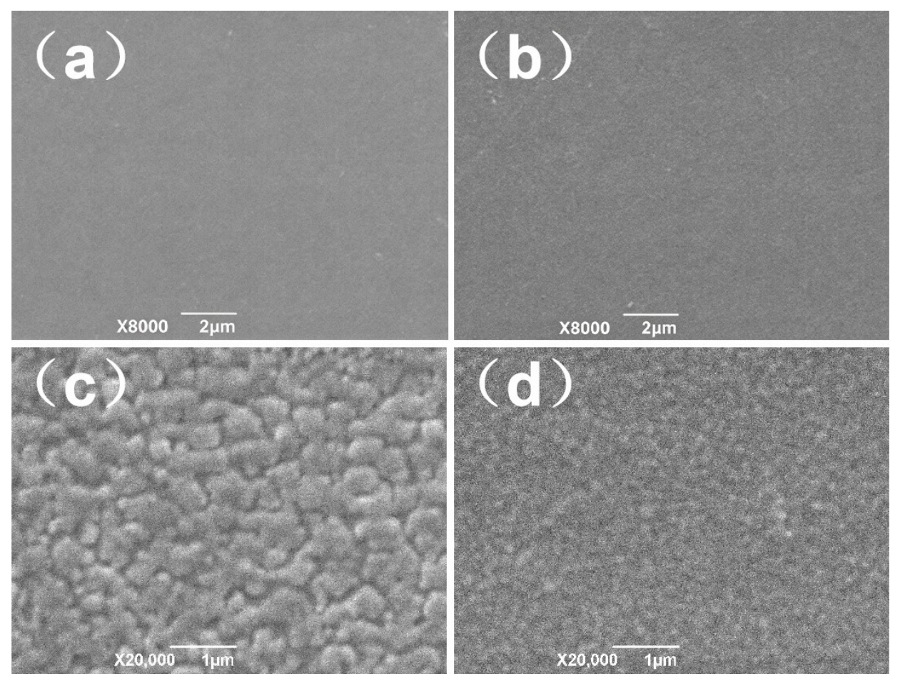
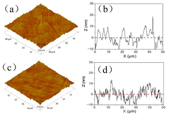
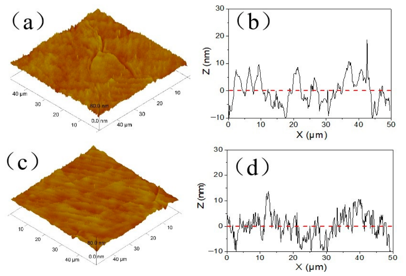
The microstructure of the Y2O3 buffer film annealed at 900 °C was characterized by SEM, as shown in Figure 2. To highlight the effect of UV irradiation on the films, comparative observation was carried out on the Y2O3 buffer film annealed at the same temperature without UV pretreatment. Figure 2a,c present the micrographs of the non-UV-irradiated sample, while Figure 2b,d correspond to the sample subjected to prior UV irradiation. In the low-magnification view (Figure 2a,b), both samples exhibit flat surfaces, and no obvious defects can be observed. However, under high-magnification observation (Figure 2c,d), significant differences can be observed. The no-UV-irradiated Y2O3 buffer film displays clearly coarse grains with large-angle grain boundaries. By contrast, the UV-irradiated Y2O3 buffer film consists of fine, uniform grains with predominantly small-angle grain boundaries. The surface roughness of the two types of Y2O3 films prepared by different processes was characterized by AFM, and the results are shown in Figure 3. The 3D topography images obtained from 40 μm × 40 μm scanning of the Y2O3 samples are shown in Figure 3a,c. It can be clearly observed that the non-UV-irradiated Y2O3 sample possesses coarse grains with prominent surface undulations. In contrast, the UV-irradiated Y2O3 sample exhibits a much smoother surface with reduced topographic fluctuations. The roughness distributions derived from 2D scanning of the two samples are presented in Figure 3b,d, and the summarized roughness parameters are listed in Table 1. The maximum surface roughness of the non-UV-irradiated Y2O3 sample is 19.8 nm, whereas the value for the UV-irradiated counterpart is only 5.46 nm.
Figure 2.
SEM images of Y2O3 buffer film annealed at 900 °C: (a) low-magnification of no-UV-irradiated, (b) low-magnification of UV-irradiated, (c) high-magnification of no-UV-irradiated (d) high-magnification of UV-irradiated.
Figure 3.
AFM of Y2O3 buffer film annealed at 900 °C: (a) no-UV-irradiated 40 μm × 40 μm 3D surface topography; (b) no-UV-irradiated 2D roughness distribution map, (c) UV-irradiated 40 μm × 40 μm 3D surface topography, (d) UV-irradiated 2D roughness distribution map.
Table 1.
The surface roughness of the Y2O3 buffer film.
3.3. FT-IR Analysis of Gel Film
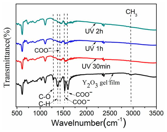
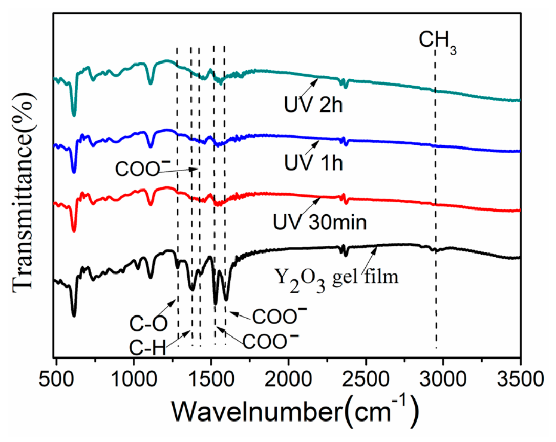
Evidently, UV irradiation is beneficial to the oriented growth of Y2O3 grains, the formation of low-angle grain boundaries, and the improvement in surface flatness. To further reveal the underlying mechanism, infrared spectroscopic analysis was performed on Y2O3 thin films subjected to different UV-irradiation durations, and the results are shown in Figure 4. The CH3 peak corresponds to the C-H stretching vibration of methyl groups in acetate and lactic acid. The COO− band at 1580 cm−1 is attributed to the asymmetric stretching vibration of carboxylate. The band at 1432 cm−1 is assigned to the symmetric stretching vibration of carboxylate. The COO− peak at 1528cm−1 originates from the asymmetric stretching vibration of lactate ligands bidentate-chelated with Y ions. The C-H band represents the C-H stretching vibration of methyl groups in lactate. In addition, although C-C bonds are undoubtedly present, the stretching vibration of C-C single bonds appears as weak bands in the fingerprint region. This signal overlaps with the C-O stretching vibration. Moreover, the dipole moment change in C-C bonds is minimal, leading to weak absorption intensity. The peak intensity gradually decreases with increasing UV-irradiation time. After 30 min of UV irradiation, the aforementioned absorption bands nearly disappeared. Further prolonging the irradiation time causes no obvious changes in other spectral bands. These results demonstrate that adsorbed water and carbonate species can be effectively removed after 30 min of UV treatment, accompanied by the decomposition of yttrium acetate.
Figure 4.
FT-IR transmission spectra of Y2O3 gel film. Symmetric stretching vibration COO− of carboxylate groups from coordinated lactate 1384 cm−1.
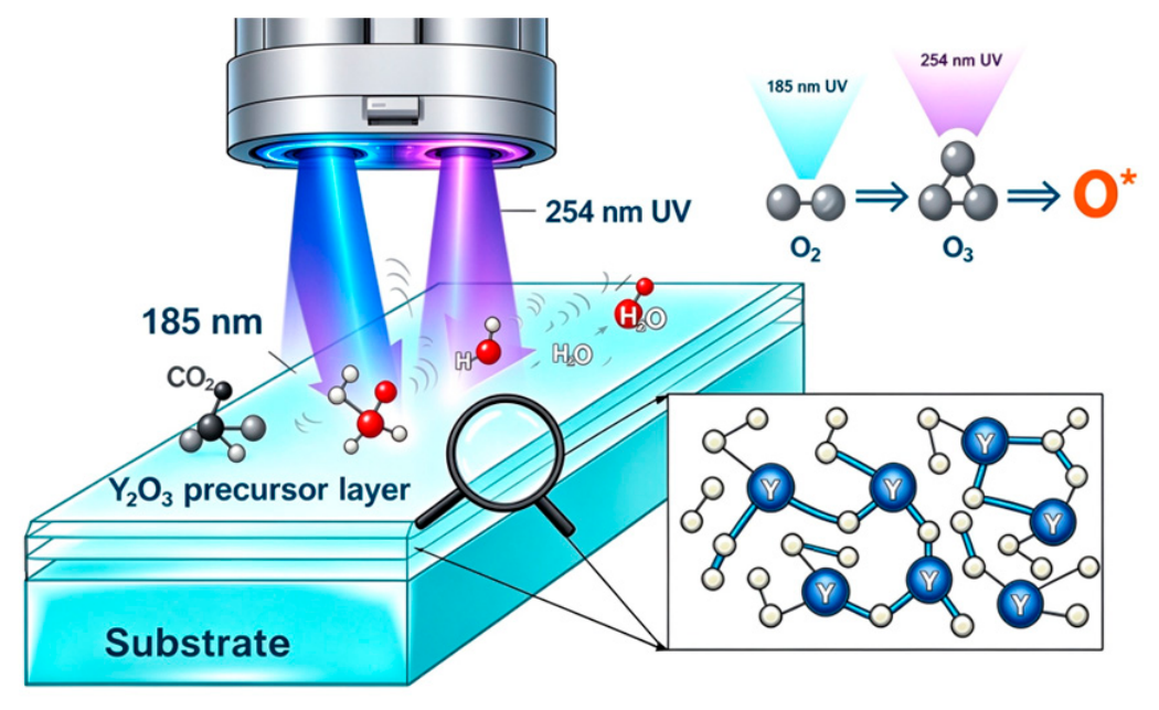
The UV wavelengths adopted in this work are 185 nm and 254 nm, with corresponding photon energies of 647 kJ/mol (185 nm) and 472 kJ/mol (254 nm), respectively. Both energy values are higher than the bond energies of C-H (413 kJ/mol), H-O (463 kJ/mol), C-O (352 kJ/mol) and C-C(348 kJ/mol) [23]. During irradiation, photochemical reaction occurs, high-energy UV light cleaves organic chemical bonds to form highly active O-M-O bonds. Owing to the bond-cleavage effect of UV irradiation, the organic species inside the film are fully decomposed at a low temperature, which prevents rapid volatilization of solvent and adsorbed water. As a result, fewer defects are formed in the film layer. Furthermore, owing to the effective penetration of UV light and its uniform decomposition of organics, agglomeration of decomposition products is inhibited, ensuring fine and uniform Y2O3 grains (as shown in Figure 2d). If the Y2O3 gel film is directly thermally decomposed without prior UV irradiation, water volatilization during heating will induce defects in the film. The escape of carbon species after organic carbonization can also give rise to film defects. Moreover, inhomogeneous heating results in decomposition products of diverse sizes, which are prone to agglomeration. Consequently, coarse Y2O3 grains are formed, accompanied by large surface undulations of the film (as shown in Figure 2c). More importantly, highly oxidative O3 and active oxygen radicals O* generated via photochemical reactions (as shown in Equations (1)–(3)) oxidize and decompose organic components. Gaseous products such as CO2 and H2O are produced and slowly and gently released from the film, leading to the formation of flat and dense Y2O3 film. The corresponding schematic diagram is shown in Figure 5.
Figure 5.
Schematic diagram of UV-irradiated Y2O3 precursor film.
Equation for O3 and O* formation under UV irradiation in air:
O2 + hv (185 nm) → O + O,
O2 + O → O3,
O3 + hv (254 nm) → O* + O2,
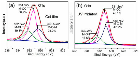
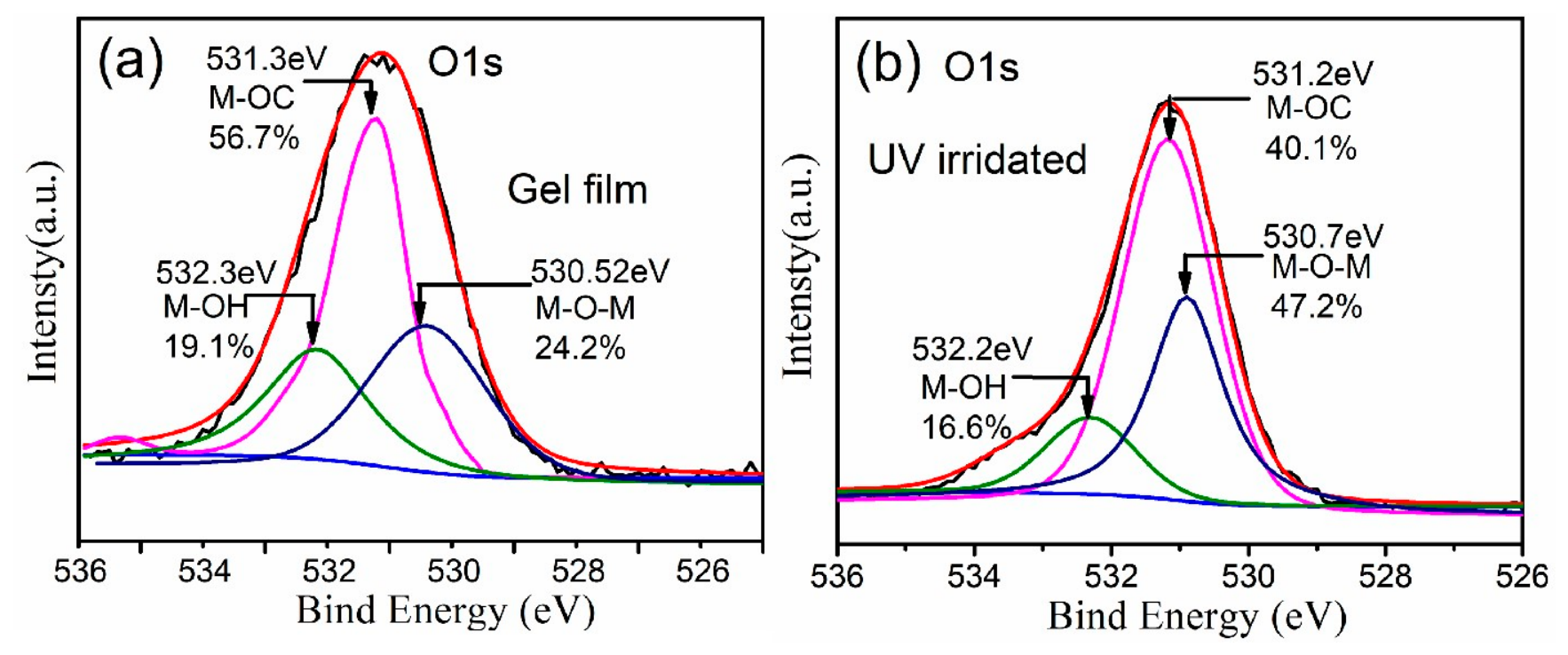
Through the above-mentioned photochemical reactions, UV light can effectively promote the decomposition of organics in the Y2O3 gel film. In addition, by-produced O3 and active oxygen radicals O* can also effectively remove the residual carbon in the form of CO2. To verify the promoting effect of UV irradiation on organic decomposition in Y2O3 gel films, XPS analysis was performed on the films before and after UV irradiation. XPS spectra were deconvoluted using CasaXPS software. The O 1s spectra of Y2O3 were recorded as shown in Figure 6. A clear decrease in Y-OH (M-OH) and Y-OC (M-OC) contents can be seen in the spectra (Figure 6b), accompanied by an increase in Y-O bond content. The increase in the integrated area fraction of the M-O-M component after UV irradiation demonstrates the rise in the relative content of Y-O-Y species on the near-surface region of the film. UV irradiation triggers photochemical decomposition of organic ligands and removes Y-OC organic oxygen species. Consequently, yttrium ions combine with oxygen to form Y-O-Y metal–oxygen bonds. It should be noted that integrated peak area fractions were adopted for quantitative analysis. This demonstrates that UV irradiation can effectively promote the decomposition of the organics in the film layer and remove residual carbon within the film. This reduces defects induced by the oxidative volatilization of carbon and guarantees the integrity of the Y2O3 film.
Figure 6.
XPS of Y2O3 gel film: (a) no-UV-irradiated; (b) UV-irradiated.
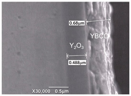
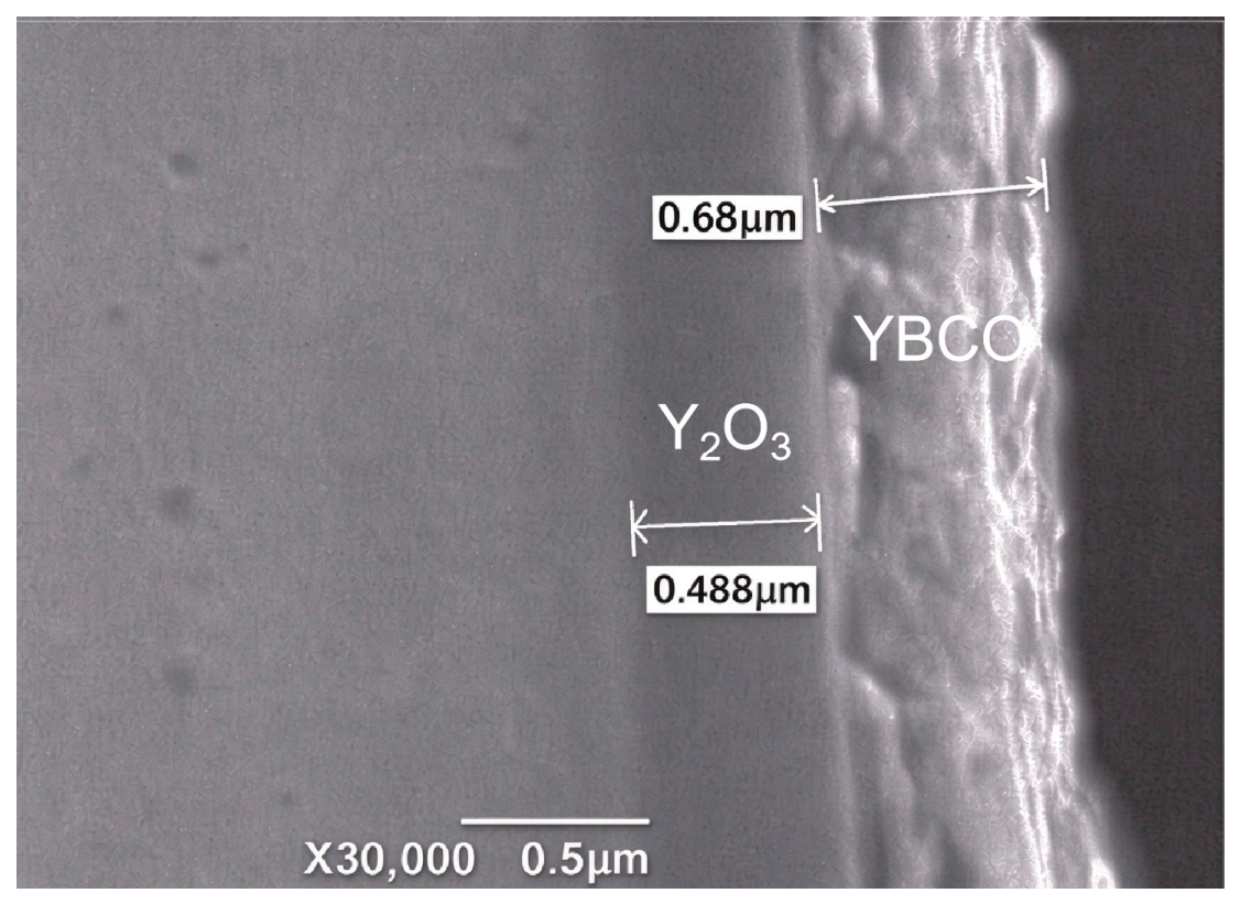
After the UV-irradiated Y2O3 gel film underwent high-temperature heat treatment at 900 °C, Y-O bonds undergo crystallization and yielded crystalline Y2O3 thin films. To facilitate the overall observation, we deposited a YBCO superconducting layer on the Y2O3 film and characterized the cross-section of the whole stack by SEM, as shown in Figure 7. The Y2O3 thin film exhibits a uniform thickness and dense microstructure, and no defects such as pores or cracks are observed. In this work, a continuous and dense Y2O3 buffer layer with a thickness of approximately 0.488 μm can be obtained after three coating cycles. This thickness is sufficient to block the diffusion paths of metallic elements. However, single- or double-layered Y2O3 films may contain tiny pinholes or hardly observable defects such as microcracks, which cannot effectively hinder the outward diffusion of Ni and W from the Ni-W substrate. Further increasing the number of coating cycles will introduce larger residual stress in the thicker Y2O3 film and consequently lead to film cracking. Meanwhile, more coating cycles will increase the fabrication cost. Therefore, three coating cycles represent the optimized processing condition in this study.
Figure 7.
Cross-sectional SEM image of the Y2O3 buffer film and YBCO film.
3.4. The Microstructure, Crystal Structure and Electrical Property of YBCO Film
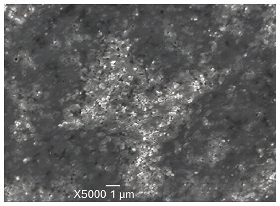
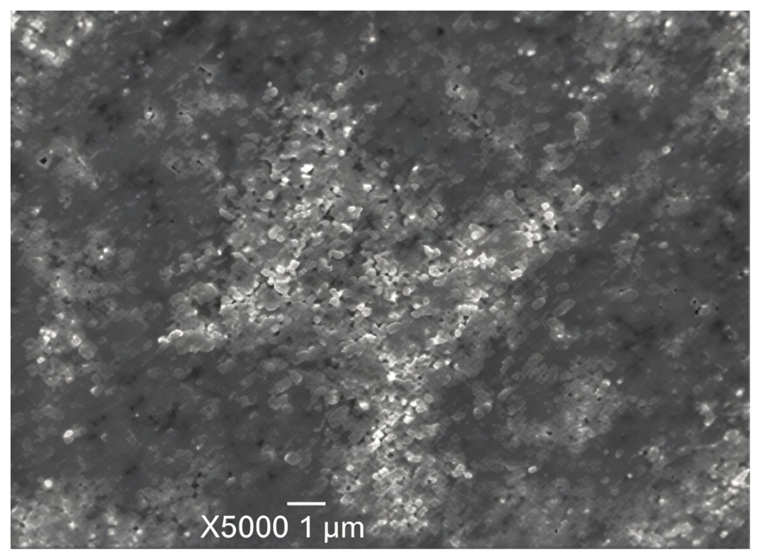
After the Y2O3 buffer film was prepared, the YBCO superconducting film was deposited on the surface of the Y2O3 buffer film. The SEM morphology of the YBCO is shown in Figure 8, and the cross-sectional SEM image is shown in Figure 7. The surface of YBCO film exhibits a flat, dense surface, and no defects such as pores are observed. The cross-sectional view reveals a dense YBCO film layer without observable defects such as pores and microcracks; the average thickness is approximately 0.68 μm.
Figure 8.
The SEM image of YBCO conducting film.
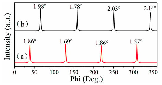
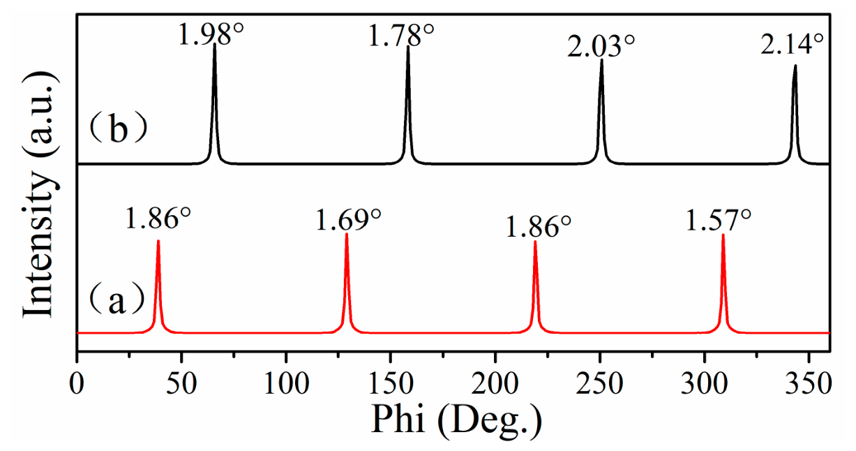
To verify whether YBCO grows epitaxially with texture on the Ni-W substrate and Y2O3 buffer film, Phi scan measurements were performed on the film surface. Y2O3 (440) and YBCO (103) reflections were chosen for in-plane Phi scan characterization. The in-plane texture of the Y2O3 and YBCO films is shown in Figure 9. Four-fold-symmetric diffraction peaks separated by 90° are observed without extra peaks. The FWHM values for Y2O3 and YBCO are 1.86°, 1.69°, 1.86° and 1.57° for the Y2O3 film and 1.98°, 1.78°, 2.03°, and 2.14° for the YBCO film, respectively, demonstrating that both Y2O3 and YBCO films achieve favorable in-plane epitaxial growth on the Ni-W substrate. The FWHM values of Y2O3 are lower than those of YBCO, revealing that Y2O3 possesses superior in-plane texture. It provides a high-quality textured template to guarantee the oriented growth of YBCO. Meanwhile, the FWHM values of YBCO are still below 2.5°, indicating that it inherits the in-plane texture from the Y2O3 barrier film, which lays a favorable crystallographic foundation for achieving a high critical current density (Jc).
Figure 9.
Phi scan of (a) Y2O3 film and (b) YBCO film.
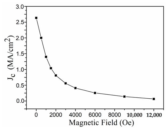
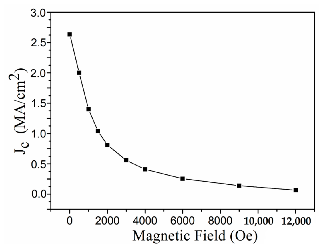
Jc measurements were performed on the YBCO film with a well-developed oriented texture, and the field-dependent critical current density Jc at 77 K are shown in Figure 10. Under the self-field condition, the sample achieves a high Jc of approximately 2.65 MA/cm2. As the applied magnetic field increases from 0 Oe to 12,000 Oe, Jc decreases monotonically. A rapid degradation of Jc is observed in the low-field region of 0–2000 Oe, while the decay becomes moderate at higher magnetic fields. A finite Jc can still be maintained even at 12,000 Oe. Such behavior is typical of high-temperature superconductors, where flux creep leads to the suppression of current-carrying capability under a magnetic field. The high self-field Jc originates from the good biaxial texture of the YBCO film. Based on the YBCO film thickness of 0.68 μm and the tape width of 10 mm, the critical current Ic at 77 K was calculated to be 180 A/cm.
Figure 10.
Jc curve of YBCO film under the different magnetic field.
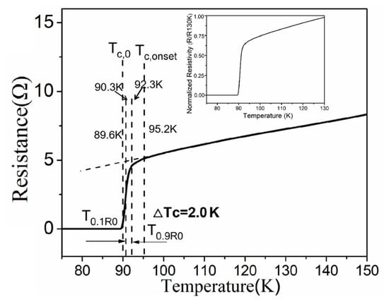
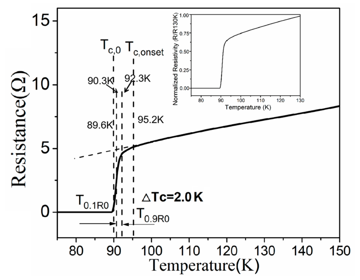
Figure 11 shows the normalized resistivity and resistance–temperature (R-T) and normalized resistivity curve of the YBCO-coated conductor measured by the four-probe method. At high temperatures, the resistance decreases approximately linearly as the temperature decreases. Upon further cooling, the resistance drops sharply and the superconducting transition occurs. The critical temperature is 95.2 K, and the YBCO superconducting transition width ΔTc, defined as the temperature difference between T0.9R and T0.1R (which correspond to 90% and 10% of the normal-state resistance, respectively), is about 2.0 K. The resistance finally falls to zero at the transition endpoint, indicating the fully superconducting state. The narrow transition width reveals high phase purity and good compositional homogeneity of the YBCO film.
Figure 11.
The resistance–temperature (R-T) curve and normalized resistivity inset of the YBCO film.
In future work, we will systematically investigate the mechanical flexibility and strain tolerance of YBCO tapes with a single-layer Y2O3 buffer. Unlike conventional multilayer buffer architectures, this simplified structure reduces heterogeneous interfaces in coated conductors, which may relieve interfacial stress concentration and improve the mechanical integrity of superconducting films upon bending. Nevertheless, the bending fatigue, critical strain and structural stability under cyclic bending require quantitative characterization. Further mechanical tests will reveal the pros and cons of photochemically prepared single-layer Y2O3 buffers for flexible high-temperature superconductors and support the practical application of low-cost YBCO tapes.
4. Conclusions
The Y2O3 buffer film and YBCO superconducting film were fabricated on Ni-W substrates by combining photochemical and sol–gel methods. The following conclusions are drawn based on the FT-IR analysis of gel films as well as the structural and property characterizations of the heat-treated coatings.
- UV photochemical treatment decomposes organic groups, removes residual carbon in the Y2O3 precursor films, promotes the formation of Y-O bonds, and mitigates defects induced by organic volatilization.
- The UV-pretreated Y2O3 film has fine and uniform grains with greatly reduced surface roughness. A dense Y2O3 buffer film, free of pores or cracks and with good biaxial in-plane texture, is obtained after annealing at 900 °C.
- The photochemically synthesized single-layer Y2O3 replicates the texture of Ni-W substrate and acts as a high-quality template for in-plane epitaxial growth of YBCO. YBCO inherits the underlying texture, with all FWHM values below 2.5°.
- YBCO-coated conductor on this Y2O3 buffer film exhibits moderate superconducting transition width and a self-field Jc of 2.65 MA/cm2 at 77 K, with typical flux-pinning performance under magnetic field. This vacuum-free technique simplifies buffer-layer architecture and is promising for low-cost fabrication of YBCO-coated conductors.
Author Contributions
J.Y.: investigation, writing—review and editing; Z.L.: investigation, data curation, writing—review; H.C.: supervision, data curation. All authors have read and agreed to the published version of the manuscript.
Funding
This research received no external funding.
Data Availability Statement
The original contributions presented in this study are included in the article. Further inquiries can be directed to the corresponding author.
Conflicts of Interest
The authors declare no conflicts of interest.
References
- Jin, J.X.; Tang, Y.J.; Xiao, X.Y.; Du, B.X.; Wang, Q.L.; Wang, J.H. HTS Power Devices and Systems: Principles, Characteristics, Performance, and Efficiency. IEEE Trans. Appl. Supercond. 2016, 26, 3800526. [Google Scholar] [CrossRef] [Scilit]
- Parizh, M.; Lvovsky, Y.; Sumption, M. Conductors for Commercial MRI Magnets Beyond NbTi: Requirements and Challenges. Supercond. Sci. Technol. 2017, 30, 014007. [Google Scholar] [CrossRef] [Scilit] [PubMed]
- Muzzi, L.; Anemona, A.; Celentano, G.; Chiarelli, S.; Della Corte, A.; De Marzi, G.; Di Zenobio, A.; Giannini, L.; Marchetti, M.; Messina, G.; et al. Design and Feasibility Assessment of an HTS Sector-Shaped High-Current Conductor for Fusion Coils. IEEE Trans. Appl. Supercond. 2023, 33, 4200106. [Google Scholar] [CrossRef] [Scilit]
- Chen, J.; Wu, W.J.; Zhou, X.H.; Huang, R.T.; Liu, Z.Y.; Li, M.J.; Wang, G.; Cai, C.B. Comprehensive Study on the Performance Evolution of BaHfO3-Added Metal-Organic Decomposition YBCO-Coated Conductors with Different Sizes and Concentrations. Supercond. Sci. Technol. 2025, 38, 065018. [Google Scholar] [CrossRef] [Scilit]
- Li, H.; Zhang, X.; Xia, Y.D.; Pan, X.F.; Peng, J.F.; Cheng, C.H.; Zhao, Y. Polymer-Assisted Chemical Solution Deposition of High-Quality La2Zr2O7 Buffer Layer Applied to Low-Cost YBCO-Coated Conductors. J. Mater. Sci. Mater. Electron. 2020, 31, 5617–5621. [Google Scholar] [CrossRef] [Scilit]
- Aye, M.M.; Rivasto, E.; Rijckaert, H.; Huhtinen, H.; Paturi, P. A Method to Enhance Thickness and Current-Carrying Capacity of BZO-Doped YBCO Multilayers. IEEE Trans. Appl. Supercond. 2025, 35, 6600506. [Google Scholar] [CrossRef] [Scilit]
- Saltarelli, L.; Sanchez Rodriguez, D.; Gupta, K.; Kethamkuzhi, A.; Farjas, J.; Molins, E.; Yañez, R.; Ricart, S.; Obradors, X.; Puig, T. Metal Propionate Solutions for High-Throughput Liquid-Assisted Manufacturing of Superconducting REBa2Cu3O7−δ (RE=Y, Gd, Sm, Yb) Films. ACS Appl. Mater. Interfaces. 2024, 16, 54199–54214. [Google Scholar] [CrossRef] [Scilit] [PubMed]
- Shipulin, I.A.; Anna Thomas, A.; Holleis, S.; Eisterer, M.; Nielsch, K.; Hühne, R. Effect of Silver Doping on the Superconducting and Structural Properties of YBCO Films Grown by PLD on Different Templates. Materials 2022, 15, 5354. [Google Scholar] [CrossRef] [Scilit] [PubMed]
- Wang, F.; Fu, W.; Huang, J.J. Industrial Pulsed Laser Deposition for Ultra-Fast Growth of High-Temperature Superconducting Thin Films with Nanostructured Pinning Centers. Supercond. Sci. Technol. 2021, 34, 080501. [Google Scholar] [CrossRef] [Scilit]
- Vannozzi, A.; Piperno, L.; Rufoloni, A.; Botti, S.; Bonfigli, F.; Lebole, M.; Savio, L.; Cialone, M.; Masi, A.; Mancini, A.; et al. Zr:CeO2 Buffer by CSD on Ni-W Substrate for Low-Cost Fe(Se,Te) Coated Conductor. IEEE Trans. Appl. Supercond. 2024, 34, 7500305. [Google Scholar] [CrossRef] [Scilit]
- Shi, D.Q.; Ko, R.K.; Song, K.J.; Chung, J.K.; Ha, H.S.; Kim, H.S.; Moon, S.H.; Yoo, S.I.; Park, C. Deposition of Y2O3 Film on Textured Metal Substrates for A Single Buffer Layer of a YBCO Coated Conductor. Supercond. Sci. Technol. 2005, 18, 561–565. [Google Scholar] [CrossRef] [Scilit]
- Pahlke, P.; Sieger, M.; Ottolinger, R.; Lao, M.; Eisterer, M.; Meledin, A.; Van Tendeloo, G.; Hänisch, J.; Holzapfel, B.; Schultz, L. Influence of Artificial Pinning Centers on Structural and Superconducting Properties of Thick YBCO Films on ABAD-YSZ Templates. Supercond. Sci. Technol. 2018, 31, 044007. [Google Scholar] [CrossRef] [Scilit]
- Xu, D.; Liu, L.F.; Xiao, G.N.; Li, Y.J. Fabrication and Characterization of La2Zr2O7 Films on Different Buffer Architectures For YBa2Cu3O7−δ Coated Conductors By RF Magnetron Sputtering. Nanoscale Res. Lett. 2013, 8, 109. [Google Scholar] [CrossRef] [Scilit] [PubMed]
- Liu, Z.; Wang, S.F.; Zhao, S.Q.; Zhou, Y.L. Epitaxial Growth of CeO2/YSZ/CeO2 Buffer Layers on Textured Ni Substrates for YBCO Conductors. J. Supercond. 2005, 18, 537–540. [Google Scholar] [CrossRef]
- Zhang, H.; Yang, J.; Liu, H.Z.; Wang, S.M. Meter-Long CeO2/YSZ/Y2O3 Buffer Layers for YBCO Coated Conductors Using DC Reactive Sputtering. Phys. C 2010, 470, 1998–2001. [Google Scholar] [CrossRef] [Scilit]
- Obradors, X.; Puig, T. Coated Conductors for Power Applications: Materials Challenges. Supercond. Sci. Technol. 2014, 27, 044003. [Google Scholar] [CrossRef] [Scilit]
- Bhuiyan, M.S.; Paranthaman, M.; Kang, S.; Lee, D.F.; Salama, K. Growth of Epitaxial Y2O3 Buffer Layers on Biaxially Textured Ni-W Substrates for YBCO Coated Conductors by MOD Approach. Phys. C 2005, 422, 95–101. [Google Scholar] [CrossRef] [Scilit]
- Xiong, J.; Xia, Y.D.; Xue, Y.; Zhang, F.; Guo, P.; Zhao, X.H.; Tao, B.W. Development of mid-frequency AC reactive magnetron sputtering for fast deposition of Y2O3 buffer layers. Phys. C 2014, 497, 38–42. [Google Scholar] [CrossRef] [Scilit]
- Barnes, P.N.; Nekkanti, R.M.; Haugan, T.J.; Campbell, T.A.; Yust, N.A.; Evans, J.M. Pulsed laser deposition of YBCO coated conductor using Y2O3 as the seed and cap layer. Supercond. Sci. Technol. 2004, 17, 957–962. [Google Scholar] [CrossRef] [Scilit][Green Version]
- Lee, S.; Kim, T.H.; Lee, Y.W.; Bae, S.Y.; Kim, S.B.; Oh, M.W.; Park, D.; Yun, Y.J.; Kim, D.W.; Bae, J.H.; et al. Selective Gelation Patterning of Solution-Processed Indium Zinc Oxide Films via Photochemical Treatments. Nanomaterials 2025, 15, 1147. [Google Scholar] [CrossRef] [Scilit] [PubMed]
- Chen, Y.Q.; Qu, W.W.; Bian, W.B.; Li, L.W.; Yerramilli, A.S.; Li, N.; Song, Y.; Wu, H.M.; Wang, A.J.; David Theodore, N.; et al. Development of Low-Fluorine Solution Route and UV Photolysis Process for YBa2Cu3O7-δ Coated Conductors. MRS Commun. 2018, 8, 1037–1042. [Google Scholar] [CrossRef] [Scilit]
- Chen, Y.Q.; Bian, W.B.; Huang, W.H.; Tang, X.N.; Zhao, G.Y.; Li, L.W. High Critical Current Density of YBa2Cu7−x Superconducting Films Prepared through a DUV-assisted Solution Deposition Process. Sci. Rep. 2016, 6, 38257. [Google Scholar] [CrossRef] [Scilit] [PubMed]
- Kim, H.J.; Kim, D.W.; Lee, W.Y.; Kim, K.D.; Lee, S.H.; Bae, J.F.; Kang, I.M.; Kim, K.E.; Jang, J.W. Flexible Sol-Gel-Processed Y2O3 RRAM Devices Obtained via UV/Ozone-Assisted Photochemical-Annealing Process. Materials 2022, 15, 1899. [Google Scholar] [CrossRef] [Scilit] [PubMed]
- Lee, S.W.; Cho, Y.J.; Heo, S.W.; Bae, J.H.; Kang, I.M.; Kim, K.E.; Lee, W.Y.; Jang, J.W. UV/Ozonge-Treated and Sol-Gel-Processed Y2O3 Insulators Prepared Using Gelation-Delaying Precursors. Nanomaterials 2024, 14, 791. [Google Scholar] [CrossRef] [Scilit] [PubMed]
- Bretos, I.; Jiménez, R.; Calzada, M.L. Photochemistry in The Low-Temperature Processing of Metal Oxide Thin Films by Solution Methods. Chem.-Eur. J. 2020, 26, 5434–5447. [Google Scholar] [CrossRef] [Scilit] [PubMed]
- Zalamova, K.; Pomar, A.; Palau, A.; Coll, M.; Puig, T.; Obradors, X. Fluorin-free Chemical Solution Deposition of YBCO Conductors From Acetate Precursor. Supercond. Sci. Technol. 2010, 23, 014012. [Google Scholar] [CrossRef] [Scilit]
- Chen, Y.Q.; Yan, F.X.; Zhao, G.Y.; Qu, G.; Lei, L. Fluorine-free Sol-Gel Preparation of YBa2Cu3O7-x Superconducting Films by A Direct Annealing Process. J. Alloy. Compd. 2010, 505, 538–542. [Google Scholar] [CrossRef] [Scilit]
- Labrag, A.; Bghour, M.; Abou EI Hassan, A.; EI Hamidi, H.; Taoufik, A.; Laasri, S. The Activation Energy U(T, B) in High Temperature Superconductor. Eur. Phys. J. Appl. Phys. 2020, 92, 20601. [Google Scholar] [CrossRef] [Scilit]

Disclaimer/Publisher’s Note: The statements, opinions and data contained in all publications are solely those of the individual author(s) and contributor(s) and not of MDPI and/or the editor(s). MDPI and/or the editor(s) disclaim responsibility for any injury to people or property resulting from any ideas, methods, instructions or products referred to in the content. |
© 2026 by the authors. Licensee MDPI, Basel, Switzerland. This article is an open access article distributed under the terms and conditions of the Creative Commons Attribution (CC BY) license.