


Abstract
Cadmium sulfide has been widely used as a conventional n-type window/buffer layer or heterojunction partner in several p-type thin-film solar cells, including CdTe/CdSeTe-, chalcopyrite-, kesterite-, antimony chalcogenide-, tin sulfide- and iron pyrite-based devices. Its success is related to its ability to form suitable heterojunctions, partially passivate absorber surfaces and provide favorable electronic selectivity. However, the parasitic absorption associated with the relatively narrow band gap of CdS, the toxicity and waste-management issues related to cadmium-containing auxiliary layers and the need for improved band alignment have motivated extensive research on CdS-free window and buffer layers. This review summarizes the main efforts devoted to replacing CdS in thin-film solar cells based on absorbers such as CdTe/CdSeTe, CIS, CIGS, CZTS, CZTSe, CZTSSe, Sb2S3, Sb2Se3, Sb2(S,Se)3, SnS and FeS2. The most investigated alternative materials, including Zn(O,S), ZnS, In2S3, ZnMgO, ZnSnO, TiO2, SnO2 and SnS2, are discussed with emphasis on their optical properties, band alignment, interface quality, deposition methods and impact on device performance. The analysis highlights that CdS replacement cannot be treated as a universal material substitution problem. Instead, each absorber and device architecture requires a specific front-interface design, where chemical compatibility, conduction band offset, defect passivation, optical transparency and process-induced interfacial modifications play a decisive role. CdS-free approaches are relatively mature for CdTe/CdSeTe- and CIGS-based solar cells, whereas kesterite absorbers, antimony chalcogenides and SnS still require further interface engineering. In FeS2, by contrast, buffer-layer substitution remains secondary to the control of intrinsic surface and bulk electronic defects. This review provides a concise comparison of the most relevant CdS-free front/window materials and identifies key challenges for the future design of sustainable thin-film solar cells.
Keywords:
thin-film solar cells; CdTe; CdSeTe; CIGS; CZTSSe kesterite; Sb2(S,Se)3; FeS2; SnS; CdS-free buffer layers; band alignment 1. Introduction
1.1. Thin-Film Photovoltaics and the Role of CdS
Thin-film photovoltaics emerged from the need to drastically reduce the amount of absorber semiconductor material required compared with crystalline silicon technology. This approach exploits direct-bandgap absorber materials with absorption coefficients on the order of 104–105 cm−1, enabling the absorption of most of the useful solar spectrum within only a few hundred nanometres to a few micrometres of material thickness [1,2]. Among the most mature thin-film photovoltaic technologies are copper indium gallium diselenide (CIGS) and cadmium telluride (CdTe). Emerging alternatives, motivated by the abundance of their constituent elements and their lower environmental impact, include Cu2ZnSn(S,Se)4 (CZTSSe) kesterites, antimony chalcogenides, tin sulfide (SnS) and iron disulphide (FeS2) in the pyrite phase. A common feature of these technologies is their heterojunction architecture, in which a p-type absorber is coupled with a wider-bandgap n-type front-interface layer, buffer layer or electron-selective contact, together with a transparent conductive oxide (TCO) in either substrate or superstrate device configurations. Throughout this review, the term window layer refers to the transparent wide-bandgap semiconductor mainly responsible for optical transmission and carrier transport, whereas buffer layer denotes the thin semiconductor located between the absorber and the window layer, whose primary functions are heterojunction formation, band alignment and interface passivation. The term electron transport layer (ETL) is used for electron-selective contacts, particularly in oxide-based architectures, while front-interface layer is adopted as a broader term encompassing any material or engineered interfacial region contributing to junction formation, carrier selectivity or interface passivation. For historical and performance-related reasons, CdS has long been the benchmark n-type front/buffer layer in many of these devices, with typical thicknesses in the range of 40–80 nm [3]. CdS can be deposited using several techniques. Chemical bath deposition (CBD) remains the most widely employed laboratory method and has enabled record device efficiencies; however, CdS can also be deposited by thermal evaporation and, in particular, by sputtering [4]. Sputtering is a dry process that can be readily integrated into in-line manufacturing, scaled to industrial production and implemented without generating the cadmium-containing chemical wastes associated with CBD, which require costly treatment and disposal systems. Similarly, other CdS-free strategies based on vacuum deposition (e.g., sputtering or ALD) generally offer improved compatibility with industrial manufacturing and avoid liquid chemical waste, although their successful implementation requires careful control of thermal budget and low-damage deposition to preserve interface quality.
Consequently, the choice of deposition technique affects not only device performance but also process sustainability, an increasingly important aspect in the transition from laboratory-scale research to large-scale manufacturing.
1.2. Limitations of CdS
Despite its technological success, CdS has several limitations, including the toxicity of cadmium, parasitic absorption due to its relatively narrow band gap, and the need for improved band alignment and interface engineering in various absorber systems. Together, these limitations have stimulated extensive research on CdS-free front layer and buffer materials and, in selected absorber systems, on alternative junction architectures aimed at reducing or even eliminating the need for a CdS layer. It should also be emphasized that the meaning of CdS replacement is absorber-dependent. In CdTe/CdSeTe-based solar cells, for example, replacing CdS refers to the development of CdS-free front interfaces rather than to the elimination of cadmium from the device, since the absorber itself contains cadmium.
1.3. Challenges of CdS Replacement: Beyond Material Substitution
More broadly, moving beyond CdS does not necessarily mean simply replacing the CdS layer with another n-type window layer. In some absorber systems, a more radical strategy is to redesign the junction architecture itself by forming buried junctions or true homojunctions within the absorber through controlled doping or surface modification. This concept has been explored in CIGS, where surface doping with Zn enabled local conductivity-type conversion and buffer-free solar cells with efficiencies around 11.5% [5]. A related buried junction has also been observed in conventional CIGS/CdS devices, with the electrically active junction located approximately 30–80 nm from the physical interface [6]. Similar buried-junction behaviour has also been reported in CdSeTe/CdTe solar cells, where interdiffusion and compositional grading contribute to an electrically active junction displaced from the nominal absorber/buffer interface [7]. Buried or quasi-buried homojunction phenomena have also been reported in CdS/Sb2Se3 and modified Sb2Se3 devices [8,9,10]. More recently, p-SnS/n-SnS homojunction solar cells have been demonstrated thanks to the development of n-type SnS, showing that CdS may become unnecessary when the junction can be formed directly within the absorber [11,12,13]. An additional aspect that deserves consideration is that CdS deposited by chemical bath deposition is not merely a passive buffer layer. In several absorber systems, particularly CIGS, CBD may induce Cd interdiffusion, near-surface doping and buried-junction formation, effects that contribute to interface passivation and favourable junction properties but are generally much less pronounced in dry-deposited alternative buffer layers. Consequently, successful CdS replacement often requires reproducing not only the electronic properties of CdS but also, where necessary, compensating for the beneficial chemical modifications introduced during interface formation. These examples broaden the concept of CdS replacement from a simple material-substitution problem to a more general strategy of interface and junction engineering.
1.4. Scope of This Review: Interface and Junction Engineering
This work adopts a critical review approach. For each absorber family, the discussion begins with the role of CdS and then examines the state of the art of Cd-free n-type buffer layers and, where experimentally demonstrated, alternative junction architectures such as buried junctions or homojunctions. Emphasis is placed on the underlying physical mechanisms, processing challenges and experimental results reported by different research groups. The motivation for moving beyond CdS is twofold. On the one hand, the RoHS Directive and REACH regulations encourage the elimination of cadmium from commercial devices. On the other hand, CdS (Eg ~2.42 eV) introduces parasitic absorption in the blue region of the solar spectrum (<520 nm), thereby limiting the short-circuit current density (Jsc), as illustrated in Figure 1a. Replacing CdS or, in selected architectures, eliminating it altogether, is therefore not only a way to reduce cadmium-containing auxiliary layers and related waste streams but also a route to improved device performance, provided that favourable band alignment, reduced parasitic absorption and effective interface passivation can be achieved at the junction [14]. As schematically illustrated in Figure 1b, the conduction-band offset (CBO) at the absorber/buffer interface is a key parameter governing charge separation and interface recombination. In general, a small positive CBO (spike) provides an energy barrier that suppresses interface recombination without significantly hindering electron transport, whereas a cliff-like alignment enhances interface recombination and typically reduces the open-circuit voltage. Therefore, the optimum CBO remains absorber- and device-dependent [15].
Figure 1.
(a) Solar AM 1.5G spectral irradiance [16] highlighting the parasitic absorption region of a standard CdS buffer layer (λ < 520 nm) and the potential current gain region accessible by wider-bandgap CdS-free alternatives. (b) Schematic conduction band alignment configurations (CBO) at the absorber/buffer heterointerface: small positive spike (ΔEc > 0), ideal flat (ΔEc = 0), and unfavorable cliff (ΔEc < 0) promoting interface recombination. The band diagrams are schematic illustrations prepared by the authors and are not drawn to scale.
From a manufacturing perspective, replacing CdS should be evaluated not only in terms of environmental sustainability but also with respect to industrial transferability. Vacuum-based approaches such as sputtering and ALD eliminate the liquid chemical waste associated with CBD and are readily compatible with in-line manufacturing. Therefore, the central question addressed in this review is not simply which material can replace CdS, but rather how absorber-specific front-interface and junction engineering can reproduce or surpass the multiple electronic, optical and chemical functions historically provided by CdS.
The literature discussed in this review was selected from peer-reviewed publications indexed in major scientific databases (primarily Scopus, Web of Science, and Google Scholar), with particular emphasis on studies published over the last 10–15 years while retaining seminal contributions that established the foundations of CdS-based heterojunctions and interface engineering. Representative device results reported in the comparative tables were selected based on their scientific relevance and the completeness of the reported photovoltaic parameters (Voc, Jsc, FF and PCE). Preference was given to studies that illustrate representative front-interface engineering strategies or significant advances in device performance. Rather than providing a systematic review, the objective is to present a critical and representative overview of the evolution of CdS replacement strategies across the main p-type thin-film photovoltaic technologies.
Within this framework, the effectiveness of CdS replacement ultimately depends on the dominant loss mechanisms of each absorber system. This absorber-specific perspective provides the conceptual basis for the comparative analysis developed throughout this review.
The main objectives are to reduce parasitic optical absorption and further optimize the front interface. In CIGS, kesterites, antimony chalcogenides and SnS, Cd-free alternatives are also pursued to improve environmental sustainability while tailoring band alignment, interface passivation and charge selectivity. By contrast, in absorber systems dominated by intrinsic material limitations, such as FeS2, buffer layer engineering plays a secondary role compared with the control of bulk and surface defects. Accordingly, this review presents CdS replacement as an absorber-specific interface and junction engineering challenge rather than a simple material substitution, providing a unified framework for comparing mature and emerging thin-film photovoltaic technologies.
2. CdTe/CdSeTe Solar Cells: From CdS Buffer Layers to CdS-Free Front Interfaces
2.1. Historical Evolution and Role of CdS
CdTe is one of the most mature and commercially successful thin-film photovoltaic technologies, thanks to its near-optimal direct band gap of approximately 1.45 eV, high optical absorption coefficient, and compatibility with large-area deposition processes. Conventional CdTe device architecture is based on a superstrate configuration, typically glass/TCO/n-type buffer/p-type CdTe/back contact. Historically, CdS has been used as the reference n-type buffer layer because it forms a robust heterojunction with CdTe, promotes favorable electronic selectivity, and is compatible with CdCl2 activation treatment, essential for grain growth, defect passivation, and junction enhancement. However, CdS also introduces parasitic absorption at short wavelengths and can limit the achievable short-circuit current density when used at the thicknesses required for complete coverage and stable junction formation. The evolution of CdTe technology efficiency has been driven by several interconnected advances, including CdCl2 activation, improved back contact engineering, doping with Cu or Group V elements, scaling of the CdSeTe/CdTe bandgap, and the replacement of CdS with wider bandgap front interface layers. The introduction of CdSeTe absorbers and advanced front buffers such as MgZnO or ZnO has enabled high current densities while preserving strong carrier selectivity at the front junction. More recently, As-doped CdSeTe/CdTe devices achieved a world-record efficiency of 22.3%, demonstrating that modern CdTe technology is now limited less by the CdS/CdTe junction itself and more by the combined optimization of absorber doping, lifetime, front interface recombination, and back contact stability [17].
2.2. CdS-Free Front Buffers and Interface Engineering
In CdTe-based solar cells, CdS substitution has a different meaning than in CIGS, kesterite, Sb2(S,Se)3, or SnS devices. Because the absorber itself contains cadmium, the transition to CdS-free front interfaces is driven primarily by optical and electronic considerations rather than the complete elimination of cadmium. The primary objectives are to reduce parasitic absorption in the blue spectral region, improve conduction band alignment at the front junction, suppress recombination at the interface, and maintain chemical compatibility with CdCl2-activated CdTe or CdSeTe absorbers. Among the most studied CdS-free front interface materials, MgxZn1−xO has played a central role. Its band gap, electron concentration, and conduction band position can be tuned by varying the Mg content, allowing for the design of the frontal interface barrier and recombination rate. However, MgZnO-based devices can exhibit anomalous J-V behavior, including S-kinks, when band alignment or contact selectivity are not properly optimized. Therefore, MgZnO is not simply a more transparent substitute for CdS, but an interface engineering layer whose composition and electronic properties must be tailored to the CdSeTe/CdTe absorber stack [18,19]. Highly resistive zinc oxide (ZnO) has also emerged as an effective CdS-free buffer for high-efficiency CdSeTe/CdTe devices. Recent ZnO/CdSeTe/CdTe solar cells have achieved efficiencies exceeding 21%, demonstrating that a wide bandgap oxide buffer can provide excellent optical transparency, stable device behavior, and a high-quality front interface when its thickness and coverage are properly controlled [20]. Recent group-V-doped Cd(Se,Te)/CdTe research cells have achieved a certified PCE of 23.1%, highlighting the continued progress of CdTe-based thin-film photovoltaics [21,22]. Other oxide-based strategies, including SnO2 and Mg-doped SnO2, have also been explored to reduce interface trap density, increase built-in potential, and improve front contact selectivity [23]. Overall, CdTe represents a relatively mature example where CdS can be widely substituted at the front interface, but successful CdS-free operation requires careful co-optimization of the transparent conductive oxide, buffer composition, absorber alloy, dopant activation, and post-deposition treatments. The main CdS replacement strategies reported for CdTe-based solar cells and their representative device performances are summarized in Table 1.
Table 1.
Representative photovoltaic parameters of CdTe/CdSeTe solar cells employing Cd-containing benchmark buffer layers, CdS-derived front-interface strategies and fully CdS-free oxide front layers. The deposition method of the front layer is indicated in parentheses (CBD = chemical bath deposition; Sput. = magnetron sputtering; ALD = atomic layer deposition). The reported energy gap (Eg) refers to the absorber material. Certified efficiencies are marked with an asterisk (*). The values should be compared with caution because absorber composition, doping, front-stack design, activation treatment and back-contact engineering differ among the cited studies.
3. CIGS: From CIS to Cadmium-Free Buffer Layers
3.1. Historical Evolution: From CuInSe2 to Cu(In,Ga)(Se,S)2
The progenitor of this absorber family is copper indium diselenide (CuInSe2, CIS), a chalcopyrite semiconductor first synthesized in the 1950s. The first photovoltaic device based on this material was developed at Bell Laboratories using CIS single crystal coupled with a CdS window layer, achieving power conversion efficiencies (PCE) on the order of 12% [30]. The subsequent transition to polycrystalline thin films occurred during the 1980s, when CIS/CdS devices fabricated by co-evaporation surpassed PCEs of 10% [31]. Among the key innovations that established CIGS as one of the most efficient thin-film photovoltaic technologies, two are particularly relevant in the context of this review. The first is alloying with gallium, Cu(In1−xGax)Se2: partial substitution of indium with gallium increases the bandgap from approximately 1.04 eV (CIS) up to ~1.68 eV (CuGaSe2), enabling optimization of the open-circuit voltage (Voc) and spectral matching for x ~0.3 (Eg ~1.15 eV), as well as enabling bandgap grading along the absorber depth, which enhances carrier collection [32]. The second innovation is the three-stage co-evaporation process developed at NREL, together with the discovery of the beneficial role of sodium originating from soda-lime glass (SLG) substrates, which improves electrical conductivity and film microstructure [33]. The progression of record efficiencies reflects these advances: 19.9% (NREL, 2008) [34], followed by the surpassing of the 20% threshold and subsequent values of 20.8% and 21.7% reported by ZSW [35,36,37], up to record devices based on sulphur-selenium alloyed Cu(In,Ga)(Se,S)2 absorbers and Cd-free buffer layers developed by Solar Frontier, culminating in a certified PCE of 23.35% [38]. It is noteworthy that several of the highest certified CIGS efficiencies, reported in recent years, have been achieved using cadmium-free buffer layers, underscoring the maturity reached by these alternative materials.
3.2. The Dual Role of CdS: Heterojunction Formation, Doping Effects and Buried Junction Formation
CdS can fulfill multiple functions in CIGS solar cells, although the relative importance depends on the deposition technique employed:
- Junction formation. CdS forms a heterojunction with p-type CIGS, often characterized by a moderate spike-like conduction-band offset (CBO). When sufficiently small, this alignment promotes electron selectivity and helps suppress interfacial recombination without significantly hindering electron transport [39].
- Doping and buried junction formation (Figure 2). During chemical bath deposition, Cd2+ ions can interact with the Cu-poor near-surface region of CIGS, where copper vacancies are abundant. Cd incorporation into Cu-related sites may locally modify the defect chemistry and promote a partial conductivity-type conversion in the absorber surface region. This chemical modification is mainly confined to the outermost region of the CIGS surface, whereas the electrically active junction does not necessarily coincide with the physical CdS/CIGS interface. Cross-sectional potential measurements have shown that the main p–n junction can be located inside the CIGS absorber, several tens of nanometres away from the heterointerface, leading to the formation of a buried junction [6,40,41]. This interfacial modification is particularly favored during chemical bath deposition, where Cd2+ ions are readily available in solution and can partially react with the absorber surface.
Figure 2.
Not-to-scale schematic representation of the heterointerface showing the typical chalcopyrite depth-dependent bandgap grading ( double-gradient profile), the -driven diffusion/interdiffusion into the -poor near-surface region of , and the resulting formation of a locally n-type region that can shift the electrically active junction away from the physical interface, giving rise to a buried junction. This figure is an original schematic drawing prepared by the authors.
This aspect is particularly relevant when evaluating Cd-free alternatives. Replacing CBD-grown CdS with a dry-deposited buffer layer does not simply modify the conduction-band alignment but may also eliminate the beneficial effects associated with Cd interdiffusion, near-surface doping and buried-junction formation. Consequently, successful Cd-free strategies should either reproduce these functions through alternative interface-engineering approaches or compensate for their absence by optimizing band alignment and interface passivation. In contrast, CdS deposited by thermal evaporation or sputtering tends to form a more abrupt physical heterojunction, with a less pronounced surface-doping effect. This distinction should be considered when comparing deposition routes, as dry processes, although more scalable and environmentally benign, may require additional interface engineering to recover the benefits associated with buried homojunction formation. By shifting the region of maximum recombination away from the defective interface, this mechanism contributes to the remarkable tolerance of CIGS devices to interfacial defects. Understanding this role of CdS is crucial when pursuing cadmium-free alternatives, since an effective replacement must either reproduce this doping-induced benefit or compensate for its absence through an appropriately engineered band alignment.
3.3. Cadmium-Free n-Type Buffer Layers for CIGS Solar Cells
Several CdS-free buffer layers have been investigated for CIGS solar cells, including Zn(O,S)-based compounds, Zn(O,S,OH), (Zn,Mg)O, In2S3, (Zn,Sn)O and related oxide or sulfide materials [14]. Their use is mainly motivated by the possibility of reducing parasitic absorption in the blue spectral region, tuning the conduction-band offset at the absorber/buffer interface and avoiding cadmium-containing wet-chemical processes. For Zn(O,S)-based layers in particular, the bandgap and conduction-band position can be adjusted by varying the O/S ratio, reducing optical losses and often increasing the short-circuit current density (Jsc) compared with CdS [42,43]. In2S3, instead, has been explored mainly as a cadmium-free sulfide buffer layer with relatively high optical transparency and compatibility with vacuum-based or low-temperature deposition processes, although its performance strongly depends on stoichiometry, defect chemistry and the resulting band alignment with CIGS [14,44]. The central challenge is the engineering of band alignment at the absorber/buffer interface. By varying the composition of Zn(O,S), the conduction-band offset (CBO) relative to CIGS can be tuned from a cliff configuration (negative offset), which is detrimental because it lowers the recombination barrier and consequently reduces Voc, to a spike configuration (moderately positive offset), which is generally considered optimal. Excessively large positive offsets, however, can hinder carrier transport. The optimal processing window is therefore narrow and strongly dependent on the gallium content at the absorber surface [45]. A further challenge is metastable behavior. Many devices employing Cd-free buffer layers require light soaking to achieve their maximum efficiency and exhibit transient effects as well as cross-over phenomena in J–V characteristics. These effects are commonly attributed to charge states located at the absorber/buffer interface and within the buffer layer itself [46]. From a processing perspective, atomic layer deposition (ALD)-grown buffers, such as Zn(O,S) and (Zn,Mg)O, provide excellent conformality and low-temperature processing capability. Chemical bath deposition (CBD), however, remains highly competitive because of its low cost and scalability, while sputtered (Zn,Mg)O is particularly attractive for fully dry, in-line manufacturing integration. Experimental results confirm the maturity of these approaches. Recent certified Cd-free CIGS record devices, reaching 23.35%, employ Zn(O,S,OH)-based buffer layers deposited by CBD, demonstrating that the elimination of cadmium does not entail a performance penalty and can, in fact, contribute to current-density gains through reduced optical losses [38]. Table 2 summarizes representative photovoltaic parameters reported in the literature. The optimal processing window is therefore narrow and strongly dependent on the gallium content at the absorber surface [45].
Table 2.
Representative photovoltaic parameters reported for CIGS solar cells employing benchmark CdS and selected CdS-free buffer layers. The deposition method of the buffer layer is indicated in parentheses (CBD = chemical bath deposition; ALD = atomic layer deposition; Evap. = in-line evaporation). Certified efficiencies are marked with an asterisk (*). The reported energy gap (Eg) refers to the buffer layer material. The values are intended to highlight representative high-performance devices and should be compared with caution, since device architecture, absorber quality, deposition conditions and interface engineering differ among the cited studies.
4. CZTS/CZTSSe Kesterite Absorbers: Toward Earth-Abundant Thin-Film Photovoltaics
4.1. Beyond Standard CdS: Motivations and Limitations
Cu2ZnSn(S,Se)4 (CZTS and CZTSSe) kesterites were conceptually derived from CIGS by replacing the costly and less abundant elements indium and gallium with zinc and tin, while preserving a closely related crystal structure and a tunable direct bandgap, ranging from approximately 1.0 eV for the pure selenide to about 1.5 eV for the pure sulfide [49]. The photovoltaic properties of CZTS were first reported by Ito and Nakazawa in 1988, who demonstrated a heterodiode based on a transparent cadmium–tin oxide/CZTS structure. Thin-film CZTS solar cells were subsequently developed by Katagiri and co-workers using a Mo/CZTS/CdS/ZnO device architecture, with initial efficiencies below 1% [50,51]. A major breakthrough toward practically relevant performance was achieved through liquid-based processing. Todorov, Reuter and Mitzi reported a high-performance liquid-processed CZTSSe solar cell with an efficiency above 9.6% [52]. This was followed by the widely cited 12.6% CZTSSe device developed at IBM through a hydrazine-based solution-processing route [53], which remained a long-standing benchmark for kesterite photovoltaics for about a decade. More recently, renewed progress in defect control, cation ordering and phase-evolution engineering has pushed CZTSSe efficiencies beyond this plateau, with a certified efficiency of 14.9% obtained through vacancy-enhanced cation ordering via Mg doping and a certified efficiency exceeding 15% achieved using a Li2SnS3 interphase strategy during selenization [54,55]. As in CIGS technology, CdS deposited by chemical bath deposition (CBD) is the benchmark buffer layer in kesterite solar cells, within a device architecture that is largely analogous to that of CIGS (substrate/Mo/absorber/CdS/i-ZnO/TCO). The fundamental limitation of kesterite devices does not primarily arise from the buffer layer itself, but rather from the large open-circuit voltage (Voc) deficit relative to the Shockley–Queisser limit. This deficit is not governed by a single loss mechanism, but results from the combined contribution of bulk defect disorder, band tailing, secondary phases, rear-interface recombination and absorber/buffer interface losses. It is generally associated with Cu/Zn antisite disorder (CuZn and ZnCu antisite defects), which induces electrostatic potential fluctuations and band tailing; the multivalence of tin (Sn2+/Sn4+) and the formation of deep defects, particularly SnZn-related defects; secondary phases such as ZnS, Cu2SnS3, and SnS(e)-based compounds; and rear-interface instabilities. At the rear interface, the formation of Mo(S,Se)2 can be beneficial when thin and well controlled, but excessive or uncontrolled growth increases series resistance and may enhance rear-interface recombination [56,57]. Within this broader loss landscape, the CdS/CZTSSe interface remains important, but should be considered as one contribution among several. Nonideal band alignment, often tending toward a cliff-like conduction-band offset, as well as interfacial chemical reactions and defect formation at the absorber/buffer interface, can further enhance recombination losses. (Figure 3).
Figure 3.
Energy diagram of a heterojunction illustrating the effect of cation disorder on electrostatic potential fluctuations and electrostatic band tailing. The diagram contrasts the conventional buffer layer, which fails to invert the kesterite surface and establishes an unfavorable cliff-like conduction band offset () that promotes severe interface recombination, with an alternative buffer configuration that successfully restores the electron transport barrier and mitigates the open-circuit voltage () deficit. The inset explicitly highlights the comparative junction physics between and kesterites, illustrating how chemical bath interdiffusion drives a robust surface inversion (buried junction) exclusively in the system. The band diagrams are schematic illustrations prepared by the authors and are not drawn to scale.
Therefore, in kesterite solar cells, moving beyond CdS requires more than replacing a cadmium-containing buffer layer. Alternative buffers must simultaneously address optical transparency, conduction-band alignment, interface passivation and chemical compatibility with an absorber that is intrinsically sensitive to defect disorder and secondary-phase formation.
4.2. Cadmium-Free Buffer Layers and Interface Engineering
Accordingly, numerous Cd-free buffer layers have been proposed for kesterite solar cells, each offering distinct advantages and limitations depending on their influence on band alignment, interface recombination and device fabrication. The most widely investigated fully Cd-free buffer layers include Zn(O,S), In2S3 and zinc–tin oxide compounds such as ZnSnO, whereas Zn1−xCdxS represents an intermediate Cd-reduced strategy rather than a truly cadmium-free alternative [58]. Among these materials, Zn(O,S) is particularly attractive because its conduction-band position can be tuned by varying the O/S ratio, allowing the absorber/buffer CBO to be shifted, depending on the CZTSSe composition, from cliff-like toward a small positive spike-like configuration. However, the high defect density of kesterite absorbers often masks the benefits of improved interface energetics, and Cd-free buffer layers on CZTSSe devices frequently exhibit greater sensitivity to post-deposition thermal treatments [59,60,61]. The most significant advances have resulted from the combined engineering of both the absorber and the heterointerface. Yan et al. achieved efficiencies exceeding 10% in pure-sulfide CZTS devices through a heterojunction heat-treatment process that modifies the interfacial region [62]. Subsequent improvements in absorber and process engineering, particularly through optimization and control of selenium partial pressure during growth, have enabled CZTSSe devices to surpass 13% certified efficiencies [63]. More recently, certified efficiencies of 14.9% and above 15% have been demonstrated, showing that further progress in kesterite photovoltaics is being driven primarily by absorber and process engineering, including defect control, cation ordering, grain-growth regulation and selenization control [54,55]. However, these best-performing devices still underline the importance of achieving a high-quality absorber/buffer interface. Therefore, Cd-free buffers should not be evaluated only in terms of optical transparency or cadmium elimination, but also according to their ability to preserve interface passivation, favorable band alignment and chemical stability. It should therefore be emphasized that CdS replacement can realistically mitigate only the front-interface contribution to the overall Voc deficit by improving conduction-band alignment, reducing interface recombination and increasing optical transmission. However, the dominant losses associated with bulk disorder, electrostatic band tailing, Sn-related deep defects, secondary phases and rear-interface recombination remain largely unaffected by the choice of buffer layer. Consequently, further efficiency improvements require simultaneous optimization of absorber quality and interface engineering. For these reasons, research on Cd-free buffer layers for kesterite solar cells remains highly active and far from complete. Table 3 summarizes representative results reported in the literature.
Table 3.
Representative photovoltaic parameters of CZTS/CZTSSe solar cells employing CdS benchmark buffers, fully Cd-free buffer layers and Cd-reduced buffer strategies. The reported energy gap (Eg) refers to the absorber material. The values should be compared with caution because absorber composition, bandgap, device architecture and post-deposition treatments differ among the cited studies.
5. Antimony Chalcogenide Absorbers: Ribbon Orientation and Cd-Free Interface Engineering
5.1. Crystal Anisotropy and Ribbon Orientation in Sb2(S,Se)3 Absorbers
Antimony chalcogenides are emerging absorber materials characterized by a strongly anisotropic quasi-one-dimensional crystal structure consisting of covalently bonded (Sb4X6)ₙ ribbons (X = S, Se) held together by weak van der Waals interactions. As depicted in Figure 4, this structural anisotropy has profound implications for charge transport: carriers move efficiently along the ribbon direction, whereas transport across adjacent ribbons is hindered by van der Waals gaps. Consequently, carrier collection, defect formation and interface recombination are strongly affected by the crystallographic orientation of the absorber, making ribbon orientation a key parameter governing photovoltaic performance [66,67]. It should also be noted that antimony chalcogenide solar cells can be fabricated in both substrate and superstrate configurations [66]. In superstrate devices, the Sb2(S,Se)3 absorber grows directly on the buffer or electron-transport layer; therefore, this underlying layer can influence not only band alignment and electron extraction, but also absorber nucleation, grain morphology and ribbon orientation [68,69,70]. In substrate devices, by contrast, the absorber is grown first on the back contact or seed layer, and the buffer layer is deposited afterwards. In this case, the buffer mainly affects the already-formed absorber surface through band alignment, interface passivation and chemical stability [71], whereas ribbon orientation is primarily governed by the back contact, seed layer and absorber growth conditions.
Figure 4.
Schematic representation of the anisotropic crystal structure and transport pathways in quasi-one-dimensional thin-film solar cells. (a) Unfavourable horizontal growth, where covalent ribbons lie parallel to the substrate, forces charge carriers to cross van der Waals gaps and can promote hopping transport through defect-rich regions. (b) Favourable vertical growth along the or direction aligns the covalently bonded ribbons perpendicular to the substrate, favouring extended-state transport, efficient carrier extraction and reduced recombination losses. This figure is an original schematic drawing prepared by the authors.
From an efficiency-evolution perspective, Sb2Se3 photovoltaics have progressed rapidly over the last decade: after early devices with efficiencies around 1–2%, the recognition of oriented quasi-one-dimensional ribbons and benign grain boundaries established the structural basis for higher-performing cells, followed by certified Sb2Se3 devices reaching 6.5% and 7.6% efficiency [72,73,74]. More recent advances in deposition kinetics, texture control, defect passivation and contact/interface engineering have pushed Sb2Se3 devices beyond the 10% threshold, with reported efficiencies of 10.12% and 10.57%, while Sb2(S,Se)3 solar cells have also recently reached certified efficiencies around 10.7% [75,76,77]. The bandgap can be tuned from approximately 1.1–1.3 eV for Sb2Se3 to about 1.7 eV for Sb2S3, while the alloy Sb2(S,Se)3 covers the intermediate range that is particularly attractive for single-junction solar cells [74]. Additional advantages of this material family include the relatively low toxicity and abundance of its constituent elements, the binary or ternary single-phase composition, which largely avoids the secondary-phase issues that plague kesterite absorbers, the high optical absorption coefficient, and good chemical stability. Historically, the first thermally evaporated thin-film Sb2Se3 solar cell employing a CdS/Sb2Se3 heterojunction achieved a power conversion efficiency of 1.9% [78]. Subsequent progress, including core–shell nanorod architectures with efficiencies around 9.2% [79] and planar or vapor-transport-deposited absorbers exceeding the 10% threshold [75], confirmed that performance improvements are strongly linked to absorber morphology, ribbon orientation and interface control. Therefore, CdS remains the benchmark n-type layer for antimony chalcogenide solar cells, particularly in superstrate architectures where it can influence both junction formation and absorber growth. However, because device performance is strongly affected by ribbon orientation, surface termination and interfacial defect passivation, CdS replacement in antimony chalcogenide solar cells cannot be considered independently from absorber growth and interface control.
5.2. Cadmium-Free Electron Transport Layers and Interface Engineering
Given the relatively early stage of Sb2(S,Se)3 photovoltaic technology, the replacement of CdS has been explored in parallel with absorber optimization, particularly with respect to ribbon orientation, surface chemistry and interface passivation. The impact of Cd-free buffer and electron-transport layers on device performance differs significantly between superstrate and substrate architectures. In superstrate Sb2(S,Se)3 solar cells, the ETL directly affects absorber nucleation and growth; therefore, Cd-free layers such as TiO2, SnO2 or ZnO can influence not only electron extraction and band alignment, but also grain morphology, ribbon orientation and defect density. As a result, improvements in Jsc and FF are often linked to enhanced vertical carrier transport, reduced shunting paths and better electron selectivity. In substrate configurations, where the absorber is already formed before buffer deposition, Cd-free layers mainly affect Voc and FF by modifying the front-interface recombination velocity, passivating surface defects and tuning the conduction-band offset. However, these layers must also avoid chemical damage or excessive interdiffusion during deposition or post-treatment, since an otherwise favourable band alignment can be offset by interface degradation. Thus, the same Cd-free material may lead to different performance trends depending on whether it acts as a growth-directing underlayer in superstrate devices or as a post-deposited passivating/selective contact in substrate devices. Cd-free electron transport layers (ETLs) investigated for Sb2(S,Se)3-based solar cells include TiO2, SnO2, ZnO, and related wide-bandgap oxides, which are typically employed in superstrate configurations [80]. A comprehensive challenge in these systems is interface energetics: band alignment at the ETL/absorber junction is strongly dependent on the S/Se ratio, which simultaneously tunes both the bandgap and the absolute band-edge positions. In particular, a cliff-like CBO can enhance interfacial recombination and limit the Voc, whereas a small positive (spike-like) offset is generally more favorable for efficient carrier extraction. Although TiO2 and SnO2 provide excellent optical transparency and chemical stability, their band alignment with Sb2(S,Se)3 is not always optimal compared with CdS, making interfacial engineering essential for performance optimization. Strategies such as surface modification of CdS, interfacial passivation, and heterojunction tuning have therefore played a key role in device improvement [81]. Regarding device performance, Sb2(S,Se)3 solar cells have reached a major milestone with a certified power conversion efficiency (PCE) of 10.0% under hydrothermal processing, as reported by Tang et al. [82]. This result established Sb2(S,Se)3 as a competitive emerging thin-film photovoltaic absorber. Subsequent improvements in absorber quality, crystallographic orientation, and interfacial engineering have enabled further incremental gains in device performance beyond this threshold [81,82]. In particular, recent work has demonstrated that thermally induced structural ordering combined with MgCl2-assisted atomic-scale defect passivation can substantially suppress deep-level defects, extend carrier lifetime and improve the electronic quality of Sb2Se3 absorbers, further highlighting the importance of coupling absorber optimization with interface engineering [83]. Notably, the highest-performing devices reported to date still rely predominantly on CdS as the electron transport layer, highlighting that CdS remains the benchmark interfacial material. This emphasizes that the development of fully competitive Cd-free ETLs requires simultaneous optimization of band alignment and interfacial passivation to replicate the beneficial electronic properties currently provided by CdS. Table 4 summarizes representative results reported in the literature. More recently, the demonstration of an internal homojunction Sb2Se3 solar cell has further expanded the concept of CdS-free junction engineering. Rather than relying on a conventional heterojunction with an external electron-transport layer, this approach creates the p-n junction directly within the absorber through polarity control, simultaneously strengthening the built-in electric field and reducing non-radiative recombination. These results further support the idea that future Sb2Se3 photovoltaics may progressively evolve from simple buffer-layer replacement toward absorber-integrated junction engineering [10].
Table 4.
Representative photovoltaic parameters of antimony chalcogenide (Sb2Se3 and Sb2(S,Se)3) solar cells employing Cd-containing benchmark ETL/buffer layers and Cd-free ETL/buffer configurations. The deposition method of the front-interface layer is indicated in parentheses (Thermal evap. = thermal evaporation; CBD = chemical bath deposition; ALD = atomic layer deposition; Spin = spin coating). The reported energy gap (Eg) refers to the absorber material. The values should be compared with caution because absorber composition, deposition conditions, device architecture (planar or nanostructured), front-interface design and back-contact engineering differ among the cited studies.
6. Interface Engineering in SnS Solar Cells
In the case of SnS-based solar cells, the comparison between CdS, alternative buffers, and possible homojunctions clearly shows that the main issue is not only the replacement of a cadmium-containing material, but also the control of the interface and band alignment. SnS/CdS devices have long been the experimental benchmark, since CdS enables the formation of an n-CdS/p-SnS heterojunction capable of separating photogenerated charges and providing a reasonable electronic selectivity; in particular, SnS/CdS cells based on absorbers grown by vapor transport deposition have achieved a certified efficiency of 4.225%, attributed to the improvement of the heterointerface quality and the reduction in interfacial defects by optimizing TCO deposition or direct annealing of the SnS/CdS interface at 300 °C [86]. However, the same study still highlights significant Jsc losses due to recombination and a high defect density associated with Sn and S vacancies, exceeding 1017 cm−3, indicating that CdS is not sufficient to overcome the intrinsic and interfacial electronic limitations of SnS [86]. In this context, alternative buffers such as Zn(O,S), Zn1−xMgxO, and more recently ZnSnO have been investigated not only to eliminate cadmium, but above all to modulate the conduction band offset, improve optical transparency, and reduce recombination at the interface. Sinsermsuksakul et al. showed that increasing the sulfur content in Zn(O,S) allows to drive the CBO towards slightly positive values, obtaining a SnS/Zn(O,S) cell with S/Zn = 0.37, Jsc = 19.4 mA cm−2, Voc = 0.244 V, FF = 42.97% and NREL certified PCE of 2.04% [87], while Ikuno et al. experimentally controlled the CBO by varying the Mg content in Zn1−xMgxO, identifying the optimal range of values between −0.1 and 0 eV and obtaining efficiencies of about 2.1% [88]. Further progress has been reported by Park et al., who achieved an efficiency of 2.9% by co-optimizing the SnS absorber and the Zn(O,S) buffer [89], while more recent results on ALD-deposited ZnSnO buffers confirm the interest in Cd-free layers capable of combining chemical control of the interface, transparency and electronic selectivity [90]. In parallel, an even more radical approach is represented by p-SnS/n-SnS homojunctions, which would eliminate the chemical discontinuity typical of heterojunctions; This strategy has historically been limited by the difficulty of obtaining stable n-type SnS, but the realization of a p-SnS/n-SnS homojunction by deposition of a polycrystalline p-type SnS film on Cl-doped n-type SnS single crystal yielded Voc = 360 mV, Jsc = 7.5 mA cm−2, FF = 53% and a PCE of 1.4%, with a built-in potential of 0.92 eV near the SnS gap, suggesting a potential advantage in terms of open-circuit voltage [13]. Subsequent advances in n-type conduction of SnS, achieved in thin films by Cl doping and stoichiometry control via sulfur plasma, together with studies on Fermi-level pinning, band bending and SnS/MoO3 interfaces, indicate that improved performance will require not only more transparent and sustainable buffers, but above all a careful control of surface states, interfacial recombination and band alignment [12,91]. Table 5 summarizes representative photovoltaic parameters reported for SnS solar cells employing conventional CdS heterojunctions, Cd-free buffer layers and homojunction architectures.
Table 5.
Representative photovoltaic parameters of SnS solar cells employing the conventional CdS buffer layer, selected Cd-free buffer layers and homojunction architectures. The deposition method of the front-interface layer is indicated in parentheses (CBD = chemical bath deposition; ALD = atomic layer deposition; Sput. = magnetron sputtering). The values should be compared with caution because absorber quality, defect density, band alignment, interface passivation and junction architecture (heterojunction or homojunction) differ among the cited studies.
7. Pyrite (FeS2): Promise and Intrinsic Limitations
Pyrite (cubic FeS2) has long been considered one of the most theoretically promising absorber materials for thin-film photovoltaics. It combines a relatively favorable narrow bandgap of approximately 0.95 eV with an exceptionally high optical absorption coefficient (>105 cm−1 above the band edge), enabling efficient photon harvesting at sub-micrometer thicknesses. In addition, its constituent elements are among the most abundant and low-cost in the Earth’s crust, making FeS2 an appealing candidate for terawatt-scale photovoltaic deployment from a materials availability perspective [92,93]. Early studies, particularly in the context of photoelectrochemical energy conversion, demonstrated strong light absorption and significant photocurrent generation, establishing the fundamental feasibility of pyrite-based solar energy conversion. Historically, FeS2 attracted strong interest because early photoelectrochemical and Schottky-type devices confirmed efficient light absorption and photocurrent generation, but subsequent solid-state photovoltaic devices failed to translate these favourable optical properties into high open-circuit voltages or competitive efficiencies. This was followed by extensive experimental efforts in the 1990s and early 2000s aimed at realizing solid-state photovoltaic devices. Despite this long-standing research interest, pyrite has consistently failed to progress beyond very low device efficiencies [92,93]. The central limitation of FeS2 lies in the severe mismatch between its excellent optical properties and its poor electronic quality. While photocarrier generation is highly efficient, device open-circuit voltages remain extremely low (typically on the order of a few hundred millivolts), corresponding to only a small fraction of the theoretical Shockley–Queisser limit [92]. This behavior reflects fundamental electronic losses that are intrinsic to the material rather than purely interfacial engineering issues. A key factor responsible for this performance collapse is the presence of a high density of intrinsic defect states, particularly sulfur vacancies and deep donor-like surface states. These defects induce strong Fermi-level pinning and lead to the formation of a surface inversion layer, which effectively short-circuits the photovoltaic junction and suppresses the achievable photovoltage [92,94]. Recent experimental evidence has also revealed the existence of an internal p–n junction within pyrite single crystals, providing a possible explanation for the anomalously low open-circuit voltages observed in FeS2 solar cells [95]. In addition, FeS2 exhibits a pronounced tendency to form secondary iron sulfide phases such as marcasite, pyrrhotite, and non-stoichiometric FeSx during synthesis, further complicating phase control and electronic passivation [92,93]. Finally, significant deviations between bulk and surface stoichiometry contribute to non-uniform band bending and additional recombination pathways [92]. Within this framework, the role of n-type buffer layers and CdS replacement strategies assumes a fundamentally different significance compared with CIGS, kesterites, and antimony chalcogenides. In those systems, device performance is strongly governed by interfacial band alignment, conduction-band offset engineering (cliff vs. spike), and buffer-mediated passivation effects. In contrast, for FeS2 the dominant bottleneck is not interface optimization but the inability of the absorber surface itself to sustain a well-defined and stable photovoltaic junction. As a result, discussions on CdS or Cd-free buffer layers are largely secondary at the current stage of development. Consequently, research efforts in pyrite photovoltaics are primarily directed toward defect engineering, surface chemistry control, and phase stabilization strategies rather than buffer layer substitution. This places FeS2 in a fundamentally different regime compared with the other thin-film absorber families discussed in this review, highlighting that the effectiveness of Cd-free window layer strategies is ultimately constrained by the intrinsic electronic quality of the absorber material. Therefore, unlike the other absorber families discussed in this review, FeS2 does not currently provide a meaningful platform for comparing CdS and Cd-free buffer layers in terms of device performance. Any future role of alternative n-type contacts will become relevant only if defect density, surface stoichiometry, Fermi-level pinning and phase purity can first be brought under sufficient control. Table 6 summarizes representative photovoltaic parameters reported for FeS2 solar cells, highlighting that device performance remains primarily limited by intrinsic material properties rather than by the choice of the front-interface layer.
Table 6.
Main performance-limiting mechanisms in FeS2 pyrite photovoltaics and their implications for Cd-containing and Cd-free front-interface strategies. The table summarizes the dominant absorber-intrinsic, surface-electronic and materials-related limitations governing FeS2 photovoltaic performance. Unlike the other absorber systems discussed in this review, device performance is presently controlled primarily by absorber quality, surface electronic structure and phase stability rather than by the choice of the front-interface layer. Therefore, direct comparisons between CdS and Cd-free front-interface layers should be interpreted with caution.
8. Discussion: The Unifying Role of Band Alignment and the Limits of CdS Replacement
To facilitate a consistent comparison among the different absorber families, the discussion is based on a comparative framework comprising four key aspects: (i) band alignment at the heterojunction, (ii) interface recombination and defect passivation, (iii) junction formation and charge-selective transport, and (iv) the resulting impact on photovoltaic performance. Although the relative importance of these factors varies among material systems, this framework provides a consistent basis for comparing mature and emerging thin-film photovoltaic technologies and for highlighting the absorber-specific challenges associated with moving beyond CdS. Analyzing the families of absorbers examined in this review (CdTe/Cd(Se,Te), CIGS, kesterites, antimony chalcogenides, SnS, and iron pyrite), a common physical principle emerges: thin-film photovoltaic performance is strongly influenced by the interplay between band alignment at the interface, selective charge transport, and defect passivation. However, the importance of these factors varies greatly from one material system to another. Across these diverse technologies, the establishment of a small, positive conduction-band offset (CBO), typically within a narrow window of approximately +0.1 to +0.3 eV (a moderate “spike”), represents the universal energetic optimum to ensure high selectivity while minimizing interface recombination. Such a moderate spike acts as an energy barrier for minority carriers, thereby suppressing their recombination at the absorber/front-interface layer interface while remaining sufficiently low to allow efficient electron transport by thermionic emission. In contrast, a cliff-like CBO lowers the interfacial recombination barrier, increasing electron-hole recombination and consequently reducing the open-circuit voltage (Voc). Consequently, mature technologies such as CdTe/Cd(Se,Te) and CIGS already demonstrate that front-interface engineering can enable the partial or complete replacement of CdS without compromising device performance, whereas in emerging absorbers the effectiveness of CdS replacement remains closely linked to absorber quality, defect chemistry, junction formation and surface stability. CdTe/Cd(Se,Te) represents a special case because replacing CdS does not eliminate cadmium from the device, but replaces the CdS window/buffer layer with wider-bandgap electron-selective front-interface materials. In this architecture, precise tuning of the Mg content is key to shifting the interface from an unfavorable negative cliff (−0.10 eV for pure ZnO) to an optimized positive spike (+0.20 eV at x ≈ 0.15), whereas excessive alloying (x > 0.35) triggers an insurmountable electron barrier up to +0.32 eV [96]. This example illustrates how the success of CdS-free CdTe architectures relies not only on replacing the buffer layer, but also on carefully engineering the front-interface band alignment to preserve the electronic functionality originally provided by CdS while reducing parasitic absorption. In CIGS technology, cadmium-free buffer layers have reached an even greater level of maturity. Materials such as Zn(O,S) and related oxides can achieve performance equal to that of CdS, and in some cases, slight improvements, primarily through reduced optical losses and optimized peak-shaped conduction band alignment. By carefully manipulating the ratio, researchers can successfully transition away from the severe cliff alignments of unalloyed and position the CBO within the favorable to spike window [97]. In this system, interface engineering has advanced enough to effectively replace CdS in several cutting-edge architectures without compromising efficiency. A different situation exists in kesterite solar cells. Although Cd-free buffers, such as Zn(O,S), In2S3, and (Zn,Sn)O, can improve band alignment and reduce parasitic absorption, notably by replacing the unfavorable cliff alignment typical of conventional CdS/CZTS interfaces (frequently reported between −0.18 eV and −0.24 eV) with a tailored spike, provided that excessive sulfur accumulation is restricted to avoid massive transport barriers [98], the main limitation remains the high open-circuit voltage deficit associated with cationic disorder, defect formation, and electrostatic potential fluctuations. Consequently, buffer layer optimization alone is insufficient to close the efficiency gap with the Shockley-Queisser limit, and CdS-based references still dominate many high-performance devices. For antimony chalcogenides, including Sb2Se3 and Sb2(S,Se)3, device performance is controlled by both interface energetics and anisotropic charge carrier transport. Their one-dimensional, ribbon-like crystalline structure makes crystallographic orientation particularly important for efficient charge extraction. Although cadmium-free electron transport layers such as TiO2, SnO2, and ZnO are actively being explored, the best-performing devices reported so far are still predominantly based on CdS, demonstrating that interface optimization, defect control, and microstructural engineering remain closely intertwined challenges. SnS solar cells occupy a less mature but scientifically instructive position. CdS has provided the benchmark heterojunction, but device performance is still limited by intrinsic defects and interfacial recombination. Alternative buffers such as Zn(O,S), Zn1−xMgxO, and ZnSnO demonstrate that engineering the conduction band mismatch can improve selectivity, where lower ratios establish the ideal small positive spike, whereas higher sulfur fractions shift the band edge to values that severely block majority carriers [99]. Although efficiencies remain modest compared to more established thin-film absorbers. At the same time, the emergence of n-type SnS and p-SnS/n-SnS homojunction concepts suggests that future advances could involve not only replacing CdS but also redesigning the junction architecture itself. Iron pyrite, FeS2, represents a fundamentally different case. Despite its attractive optical properties, including a narrow band gap, high absorption coefficient, and naturally abundant composition, photovoltaic performance remains severely limited by intrinsic surface and bulk electronic defects. Sulfur vacancies, deep donor states, and Fermi-level pinning suppress Voc and can promote surface inversion, short-circuiting the junction rendering buffer layer optimization largely ineffective. The comparison presented in Figure 5 highlights that the effectiveness of CdS replacement is strongly absorber-dependent and can be broadly classified into three categories according to the dominant performance-limiting mechanisms. The first includes absorber systems such as CdTe/CdSeTe and CIGS, where front-interface recombination and band alignment represent the principal challenges and can be effectively addressed through front-interface engineering. The other four comprise CZTS/CZTSSe, Sb2Se3, Sb2(S,Se)3 and SnS absorbers, in which both interface-related losses and bulk defects contribute significantly to the overall performance limitation, requiring simultaneous optimization of absorber quality and junction design. Finally, FeS2 represents the limiting case where intrinsic surface and bulk electronic defects dominate device behavior, making buffer layer replacement alone insufficient to achieve substantial efficiency improvements.
Figure 5.
Schematic comparison of CdS-replacement maturity and dominant performance-limiting mechanisms in different thin-film absorber families. CdTe/Cd(Se,Te) and CIGS represent the most mature cases for CdS-free front-interface engineering, while kesterites, antimony chalcogenides and SnS remain limited by combined interface and absorber-related losses. FeS2 represents the limiting case where intrinsic surface and bulk electronic defects make buffer-layer replacement secondary. This conceptual schematic was originally prepared by the authors. The position of each absorber family reflects the relative importance of front-interface engineering and intrinsic absorber limitations, ranging from systems mainly limited by front-interface recombination and band alignment to those dominated by intrinsic absorber defects.
9. Conclusions
The long-standing success of CdS in thin-film photovoltaics arises from the combination of multiple optical, electronic and chemical functions, including favorable junction formation, suitable band alignment, interfacial passivation, chemical compatibility and process robustness. Consequently, replacing CdS cannot be regarded as the simple substitution of one material by another, but rather as the reconstruction of the multifunctional role that CdS has historically played at the front interface. As discussed throughout this review, the feasibility of CdS replacement is strongly absorber-dependent. CdS-free architectures have already demonstrated technological maturity when optical losses and front-interface recombination are the dominant limitations, whereas systems limited by bulk disorder, metastability, unfavorable defect chemistry or surface electronic instability require broader materials and interface optimization beyond buffer-layer replacement alone. Future progress will therefore rely on predictive absorber-specific interface engineering rather than empirical buffer substitution. Compositionally tuneable oxides and chalcogenides, atomic-scale passivation, controlled interdiffusion and scalable low-damage deposition processes are expected to play a central role in developing front interfaces that simultaneously provide optimized band alignment, defect passivation, optical transparency, chemical stability and manufacturability. In this perspective, the transition beyond CdS should be viewed not simply as the replacement of a conventional material, but as the development of absorber-specific junction architectures capable of delivering higher efficiency together with improved sustainability.
Author Contributions
Conceptualization, A.B. and S.P.; Validation, A.B.; Writing—original draft, S.P. and A.B.; Writing—review & editing, S.P., A.B., S.R. and M.K.; Supervision A.B. All authors have read and agreed to the published version of the manuscript.
Funding
This research received no external funding.
Data Availability Statement
No new data were created or analyzed in this study. Data sharing is not applicable to this article.
Conflicts of Interest
The authors declare no conflict of interest.
References
- Polman, A.; Knight, M.; Garnett, E.C.; Ehrler, B.; Sinke, W.C. Photovoltaic Materials: Present Efficiencies and Future Challenges. Science 2016, 352, aad4424. [Google Scholar] [CrossRef] [Scilit] [PubMed]
- Green, M.A.; Dunlop, E.D.; Yoshita, M.; Kopidakis, N.; Bothe, K.; Siefer, G.; Hao, X.; Jiang, J.Y. Solar Cell Efficiency Tables (Version 66). Prog. Photovolt. Res. Appl. 2025, 33, 795–810. [Google Scholar] [CrossRef] [Scilit]
- Hariskos, D.; Spiering, S.; Powalla, M. Buffer Layers in Cu(In,Ga)Se2 Solar Cells and Modules. Thin Solid Films 2005, 480–481, 99–109. [Google Scholar] [CrossRef] [Scilit]
- Romeo, N.; Bosio, A.; Tedeschi, R.; Canevari, V. Growth of Polycrystalline CdS and CdTe Thin Layers for High Efficiency Thin Film Solar Cells. Mater. Chem. Phys. 2000, 66, 201–206. [Google Scholar] [CrossRef] [Scilit]
- Takeshi Sugiyama, T.S.; Sutichai Chaisitsak, S.C.; Akira Yamada, A.Y.; Makoto Konagai, M.K.; Yuriy Kudriavtsev, Y.K.; Antonio Godines, A.G.; Antonio Villegas, A.V.; Rene Asomoza, R.A. Formation of Pn Homojunction in Cu(InGa)Se2 Thin Film Solar Cells by Zn Doping. Jpn. J. Appl. Phys. 2000, 39, 4816. [Google Scholar] [CrossRef] [Scilit]
- Jiang, C.-S.; Hasoon, F.S.; Moutinho, H.R.; Al-Thani, H.A.; Romero, M.J.; Al-Jassim, M.M. Direct Evidence of a Buried Homojunction in Cu(In,Ga)Se2 Solar Cells. Appl. Phys. Lett. 2003, 82, 127–129. [Google Scholar] [CrossRef] [Scilit]
- Jiang, H.; Cai, Y.; Wang, G.; Yi, K.; Liu, F.; Tian, J.; Shen, K.; Wang, D. Buried Junction and Efficient Carrier Separation in CdSexTe1−x/CdTe Solar Cells. J. Appl. Phys. 2024, 135, 143102. [Google Scholar] [CrossRef] [Scilit]
- Zhou, Y.; Li, Y.; Luo, J.; Li, D.; Liu, X.; Chen, C.; Song, H.; Ma, J.; Xue, D.-J.; Yang, B.; et al. Buried Homojunction in CdS/Sb2Se3 Thin Film Photovoltaics Generated by Interfacial Diffusion. Appl. Phys. Lett. 2017, 111, 013901. [Google Scholar] [CrossRef] [Scilit]
- Ren, D.; Chen, S.; Cathelinaud, M.; Liang, G.; Ma, H.; Zhang, X. Fundamental Physical Characterization of Sb2Se3-Based Quasi-Homojunction Thin Film Solar Cells. ACS Appl. Mater. Interfaces 2020, 12, 30572–30583. [Google Scholar] [CrossRef] [Scilit] [PubMed]
- Yang, J.; Li, J.; Sheng, S.; Cai, Z.; Li, K.; Ruan, Z.; Che, B.; Tang, R.; Chen, T. Internal Homojunction Sb2Se3 Solar Cell. Nat. Photonics 2026, 20, 644–652. [Google Scholar] [CrossRef] [Scilit]
- Suzuki, I.; Kawanishi, S.; Omata, T.; Yanagi, H. Current Status of N-Type SnS: Paving the Way for SnS Homojunction Solar Cells. J. Physics. Energy 2022, 4, 042002. [Google Scholar] [CrossRef] [Scilit]
- Suzuki, I.; Kawanishi, S.; Bauers, S.R.; Zakutayev, A.; Lin, Z.; Tsukuda, S.; Shibata, H.; Kim, M.; Yanagi, H.; Omata, T. N-Type Electrical Conduction in SnS Thin Films. Phys. Rev. Mater. 2021, 5, 125405. [Google Scholar] [CrossRef] [Scilit]
- Kawanishi, S.; Suzuki, I.; Bauers, S.R.; Zakutayev, A.; Shibata, H.; Yanagi, H.; Omata, T. SnS Homojunction Solar Cell with N-Type Single Crystal and P-Type Thin Film. Sol. RRL 2021, 5, 2000708. [Google Scholar] [CrossRef] [Scilit]
- Naghavi, N.; Abou-Ras, D.; Allsop, N.; Barreau, N.; Bücheler, S.; Ennaoui, A.; Fischer, C.H.; Guillen, C.; Hariskos, D.; Herrero, J.; et al. Buffer Layers and Transparent Conducting Oxides for Chalcopyrite Cu(In,Ga)(S,Se)2 Based Thin Film Photovoltaics: Present Status and Current Developments. Prog. Photovolt. Res. Appl. 2010, 18, 411–433. [Google Scholar] [CrossRef] [Scilit]
- Song, T.; Kanevce, A.; Sites, J.R. Emitter/Absorber Interface of CdTe Solar Cells. J. Appl. Phys. 2016, 119, 233104. [Google Scholar] [CrossRef] [Scilit]
- ASTM G173-03; Tables for Reference Solar Spectral Irradiances: Direct Normal and Hemispherical on 37 Tilted Surface 2020. ASTM International: West Conshohoken, PA, USA, 2021.
- Mallick, R.; Li, X.; Reich, C.; Shan, X.; Zhang, W.; Nagle, T.; Bok, L.; Bicakci, E.; Rosenblatt, N.; Modi, D.; et al. Arsenic-Doped CdSeTe Solar Cells Achieve World Record 22.3% Efficiency. IEEE J. Photovolt. 2023, 13, 510–515. [Google Scholar] [CrossRef] [Scilit]
- Ablekim, T.; Colegrove, E.; Metzger, W.K. Interface Engineering for 25% CdTe Solar Cells. ACS Appl. Energy Mater. 2018, 1, acsaem.8b01173. [Google Scholar] [CrossRef] [Scilit]
- Ablekim, T.; Perkins, C.; Zheng, X.; Reich, C.; Swanson, D.; Colegrove, E.; Duenow, J.N.; Albin, D.; Nanayakkara, S.; Reese, M.O.; et al. Tailoring MgZnO/CdSeTe Interfaces for Photovoltaics. IEEE J. Photovolt. 2019, 9, 888–892. [Google Scholar] [CrossRef] [Scilit]
- Kujovic, L.; Liu, X.; Abbas, A.; Jones, L.O.; Law, A.M.; Togay, M.; Curson, K.M.; Barth, K.L.; Bowers, J.W.; Walls, J.M.; et al. Achieving 21.4% Efficient CdSeTe/CdTe Solar Cells Using Highly Resistive Intrinsic ZnO Buffer Layers. Adv. Funct. Mater. 2024, 34, 2312528. [Google Scholar] [CrossRef] [Scilit]
- Available online: https://www.nlr.gov/Pv/Interactive-Cell-Efficiency (accessed on 13 July 2026).
- Sartor, B.E.; Reese, S.B.; Mansfield, L.M.; Muzzio, R.; Jiang, C.-S.; Colegrove, E.; Mangum, J.S.; Kasik, C.L.; Shaw, D.Z.; Sites, J.R.; et al. Roadmap to 100 GWDC: Scientific and Supply Chain Challenges for CdTe Photovoltaics. Joule 2026, 10, 102235. [Google Scholar] [CrossRef] [Scilit]
- Cai, Y.; Liu, C.; Jiang, H.; Yi, K.; Liu, F.; Wang, D. Interfacial Passivation of CdTe Solar Cells Using Mg-Doped SnO2 as Electron Transport Layer for Enhanced Photovoltaic Efficiency. J. Appl. Phys. 2025, 137, 043102. [Google Scholar] [CrossRef] [Scilit]
- Wu, X. High-Efficiency Polycrystalline CdTe Thin-Film Solar Cells. Sol. Energy 2004, 77, 803–814. [Google Scholar] [CrossRef] [Scilit]
- Scarpulla, M.A.; McCandless, B.; Phillips, A.B.; Yan, Y.; Heben, M.J.; Wolden, C.; Xiong, G.; Metzger, W.K.; Mao, D.; Krasikov, D.; et al. CdTe-Based Thin Film Photovoltaics: Recent Advances, Current Challenges and Future Prospects. Sol. Energy Mater. Sol. Cells 2023, 255, 112289. [Google Scholar] [CrossRef] [Scilit]
- Munshi, A.H.; Kephart, J.; Abbas, A.; Raguse, J.; Beaudry, J.-N.; Barth, K.; Sites, J.; Walls, J.; Sampath, W. Polycrystalline CdSeTe/CdTe Absorber Cells with 28 mAcm2 Short-Circuit Current. IEEE J. Photovolt. 2018, 8, 310–314. [Google Scholar] [CrossRef] [Scilit]
- Li, D.-B.; Bista, S.S.; Awni, R.A.; Neupane, S.; Abudulimu, A.; Wang, X.; Subedi, K.K.; Jamarkattel, M.K.; Phillips, A.B.; Heben, M.J.; et al. 20%-Efficient Polycrystalline Cd(Se,Te) Thin-Film Solar Cells with Compositional Gradient near the Front Junction. Nat. Commun. 2022, 13, 7849. [Google Scholar] [CrossRef] [Scilit] [PubMed]
- Infante-Ortega, L.C.; Liu, X.; Kujovic, L.; Togay, M.; Jones, L.O.; Abbas, A.; Bowers, J.W.; Walls, J.M.; Zhang, W.; Lee, C.; et al. Optimising the Thickness of Sputtered SnO2 Buffer Layers for High Efficiency CdSeTe/CdTe Devices. In Proceedings of the 2024 IEEE 52nd Photovoltaic Specialist Conference (PVSC), Seattle, WA, USA, 9–14 June 2024; pp. 1387–1389. [Google Scholar]
- Liu, X.; Kujovic, L.; Zhou, Z.; Robertson, S.; Togay, M.; Kenyon, J.; Infante-Ortega, L.C.; Bliss, M.; Bowers, J.W.; Walls, J.M.; et al. Improved Interface Passivation in High-Efficiency Se-Alloyed CdTe Solar Cells Using a SnO2/ZnO n-Type Bilayer. Sol. Energy Mater. Sol. Cells 2026, 297, 114139. [Google Scholar] [CrossRef] [Scilit]
- Wagner, S.; Shay, J.L.; Migliorato, P.; Kasper, H.M. CuInSe2/CdS Heterojunction Photovoltaic Detectors. Appl. Phys. Lett. 1974, 25, 434435. [Google Scholar] [CrossRef] [Scilit]
- Mickelsen, R.A.; Chen, W.S. High Photocurrent Polycrystalline Thin-Film CdS/CuInSe2 Solar Cella. Appl. Phys. Lett. 1980, 36, 371–373. [Google Scholar] [CrossRef] [Scilit]
- Contreras, M.A.; Egaas, B.; Ramanathan, K.; Hiltner, J.; Swartzlander, A.; Hasoon, F.; Noufi, R. Progress toward 20% Efficiency in Cu(In,Ga)Se2 Polycrystalline Thin-Film Solar Cells. Prog. Photovolt. Res. Appl. 1999, 7, 311–316. [Google Scholar] [CrossRef]
- Rau, U.; Schock, H.W. Electronic Properties of Cu(In,Ga)Se2 Heterojunction Solar Cells-Recent Achievements, Current Understanding, and Future Challenges. Appl. Phys. A Mater. Sci. Process. 1999, 69, 131–147. [Google Scholar] [CrossRef] [Scilit]
- Repins, I.; Contreras, M.A.; Egaas, B.; DeHart, C.; Scharf, J.; Perkins, C.L.; To, B.; Noufi, R. 19.9%-efficient ZnO/CdS/CuInGaSe2 Solar Cell with 81.2% Fill Factor. Prog. Photovolt. Res. Appl. 2008, 16, 235–239. [Google Scholar] [CrossRef] [Scilit]
- Jackson, P.; Hariskos, D.; Lotter, E.; Paetel, S.; Wuerz, R.; Menner, R.; Wischmann, W.; Powalla, M. New World Record Efficiency for Cu(In,Ga)Se2 Thin-film Solar Cells beyond 20%. Prog. Photovolt. Res. Appl. 2011, 19, 894–897. [Google Scholar] [CrossRef] [Scilit]
- Jackson, P.; Wuerz, R.; Hariskos, D.; Lotter, E.; Witte, W.; Powalla, M. Effects of Heavy Alkali Elements in Cu(In,Ga)Se2 Solar Cells with Efficiencies up to 22.6%. Phys. Status Solidi RRL 2016, 10, 583–586. [Google Scholar] [CrossRef] [Scilit]
- Jackson, P.; Hariskos, D.; Wuerz, R.; Kiowski, O.; Bauer, A.; Friedlmeier, T.M.; Powalla, M. Properties of Cu(In,Ga)Se2 Solar Cells with New Record Efficiencies up to 21.7%. Phys. Status Solidi RRL 2015, 9, 28–31. [Google Scholar] [CrossRef] [Scilit]
- Nakamura, M.; Yamaguchi, K.; Kimoto, Y.; Yasaki, Y.; Kato, T.; Sugimoto, H. Cd-Free Cu(In,Ga)(Se,S)2 Thin-Film Solar Cell With Record Efficiency of 23.35%. IEEE J. Photovolt. 2019, 9, 1863–1867. [Google Scholar] [CrossRef] [Scilit]
- Klenk, R. Characterisation and Modelling of Chalcopyrite Solar Cells. Thin Solid Films 2001, 387, 135–140. [Google Scholar] [CrossRef] [Scilit]
- Nakada, T.; Kunioka, A. Direct Evidence of Cd Diffusion into Cu(In, Ga)Se2 Thin Films during Chemical-Bath Deposition Process of CdS Films. Appl. Phys. Lett. 1999, 74, 2444–2446. [Google Scholar] [CrossRef] [Scilit]
- Abou-Ras, D.; Kostorz, G.; Romeo, A.; Rudmann, D.; Tiwari, A.N. Structural and Chemical Investigations of CBD- and PVD-CdS Buffer Layers and Interfaces in Cu(In,Ga)Se2-Based Thin Film Solar Cells. Thin Solid Films 2005, 480–481, 118–123. [Google Scholar] [CrossRef] [Scilit]
- Bhattacharya, R.N.; Contreras, M.A.; Teeter, G. 18.5% Copper Indium Gallium Diselenide (CIGS) Device Using Single-Layer, Chemical-Bath-Deposited ZnS(O,OH). Jpn. J. Appl. Phys. 2004, 43, L1475–L1476. [Google Scholar] [CrossRef] [Scilit]
- Bhattacharya, R.N.; Ramanathan, K.; Gedvilas, L.; Keyes, B. Cu(In,Ga)Se2 Thin-Film Solar Cells with ZnS(O,OH), Zn–Cd–S(O,OH), and CdS Buffer Layers. J. Phys. Chem. Solids 2005, 66, 1862–1864. [Google Scholar] [CrossRef] [Scilit]
- Spiering, S.; Nowitzki, A.; Kessler, F.; Igalson, M.; Abdel Maksoud, H. Optimization of Buffer-Window Layer System for CIGS Thin Film Devices with Indium Sulphide Buffer by in-Line Evaporation. Sol. Energy Mater. Sol. Cells 2016, 144, 544–550. [Google Scholar] [CrossRef] [Scilit]
- Minemoto, T.; Matsui, T.; Takakura, H.; Hamakawa, Y.; Negami, T.; Hashimoto, Y.; Uenoyama, T.; Kitagawa, M. Theoretical Analysis of the Effect of Conduction Band Offset of Window/CIS Layers on Performance of CIS Solar Cells Using Device Simulation. Sol. Energy Mater. Sol. Cells 2001, 67, 83–88. [Google Scholar] [CrossRef] [Scilit]
- Pudov, A.O.; Kanevce, A.; Al-Thani, H.A.; Sites, J.R.; Hasoon, F.S. Secondary Barriers in CdS–CuIn1−xGaxSe2 Solar Cells. J. Appl. Phys. 2005, 97, 064901. [Google Scholar] [CrossRef] [Scilit]
- Pettersson, J.; Platzer-Björkman, C.; Edoff, M. Temperature-dependent Current-voltage and Lightsoaking Measurements on Cu(In,Ga)Se2 Solar Cells with ALD-Zn1-xMgxO Buffer Layers. Prog. Photovolt. Res. Appl. 2009, 17, 460–469. [Google Scholar] [CrossRef] [Scilit]
- Salomé, P.M.P.; Keller, J.; Törndahl, T.; Teixeira, J.P.; Nicoara, N.; Andrade, R.-R.; Stroppa, D.G.; González, J.C.; Edoff, M.; Leitão, J.P.; et al. CdS and Zn1−xSnxOy Buffer Layers for CIGS Solar Cells. Sol. Energy Mater. Sol. Cells 2017, 159, 272–281. [Google Scholar] [CrossRef] [Scilit]
- Siebentritt, S.; Schorr, S. Kesterites—A Challenging Material for Solar Cells. Prog. Photovolt. Res. Appl. 2012, 20, 512–519. [Google Scholar] [CrossRef] [Scilit]
- Katagiri, H.; Sasaguchi, N.; Hando, S.; Hoshino, S.; Ohashi, J.; Yokota, T. Preparation and Evaluation of Cu2ZnSnS4 Thin Films by Sulfurization of E B Evaporated Precursors. Sol. Energy Mater. Sol. Cells 1997, 49, 407–414. [Google Scholar] [CrossRef] [Scilit]
- Nakazawa, K.I. Electrical and Optical Properties of Stannite-Type Quaternary Semiconductor Thin Films. Jpn. J. Appl. Phys. 1988, 27, 2094. [Google Scholar] [CrossRef] [Scilit]
- Todorov, T.K.; Reuter, K.B.; Mitzi, D.B. High-Efficiency Solar Cell with Earth-Abundant Liquid-Processed Absorber. Adv. Mater. 2010, 22, E156–E159. [Google Scholar] [CrossRef] [Scilit] [PubMed]
- Wang, W.; Winkler, M.T.; Gunawan, O.; Gokmen, T.; Todorov, T.K.; Zhu, Y.; Mitzi, D.B. Device Characteristics of CZTSSe Thin-Film Solar Cells with 12.6% Efficiency. Adv. Energy Mater. 2014, 4, 1301465. [Google Scholar] [CrossRef] [Scilit]
- Wang, J.; Meng, F.; Lou, L.; Yin, K.; Xu, X.; Jiao, M.; Zhang, B.; Li, Y.; Shi, J.; Wu, H.; et al. Vacancy-Enhanced Cation Ordering via Magnesium Doping to Enable Kesterite Solar Cells with 14.9% Certified Efficiency. Nat. Energy 2025, 11, 66–75. [Google Scholar] [CrossRef] [Scilit]
- Cui, C.; Li, Y.; Wei, H.; Du, X.; Shao, Z.; Kou, D.; Wu, Z.; Xia, S.; Feng, X.; Pang, S.; et al. Regulating Grain Growth via Li2SnS3 Interphase in Kesterite Solar Cells with Certified Efficiencies Exceeding 15%. Nat. Energy 2026, 11, 460–469. [Google Scholar] [CrossRef] [Scilit]
- Gokmen, T.; Gunawan, O.; Todorov, T.K.; Mitzi, D.B. Band Tailing and Efficiency Limitation in Kesterite Solar Cells. Appl. Phys. Lett. 2013, 103, 103506. [Google Scholar] [CrossRef] [Scilit]
- Schorr, S. The Crystal Structure of Kesterite Type Compounds: A Neutron and X-Ray Diffraction Study. Sol. Energy Mater. Sol. Cells 2011, 95, 1482–1488. [Google Scholar] [CrossRef] [Scilit]
- Bär, M.; Schubert, B.-A.; Marsen, B.; Wilks, R.G.; Pookpanratana, S.; Blum, M.; Krause, S.; Unold, T.; Yang, W.; Weinhardt, L.; et al. Cliff-like Conduction Band Offset and KCN-Induced Recombination Barrier Enhancement at the CdS/Cu2ZnSnS4 Thin-Film Solar Cell Heterojunction. Appl. Phys. Lett. 2011, 99, 222105. [Google Scholar] [CrossRef] [Scilit]
- Hironiwa, D.; Matsuo, N.; Sakai, N.; Katou, T.; Sugimoto, H.; Chantana, J.; Tang, Z.; Minemoto, T. Sputtered (Zn,Mg)O Buffer Layer for Band Offset Control in Cu2ZnSn(S,Se)4 Solar Cells. Jpn. J. Appl. Phys. 2014, 53, 106502. [Google Scholar] [CrossRef] [Scilit]
- Hironiwa, D.; Matsuo, N.; Chantana, J.; Sakai, N.; Kato, T.; Sugimoto, H.; Minemoto, T. Annealing Effect on Cu2ZnSn(S,Se)4 Solar Cell with Zn1–XMgxO Buffer Layer. Phys. Status Solidi A 2015, 212, 2766–2771. [Google Scholar] [CrossRef] [Scilit]
- Hironiwa, D.; Sakai, N.; Kato, T.; Sugimoto, H.; Tang, Z.; Chantana, J.; Minemoto, T. Impact of Annealing Treatment before Buffer Layer Deposition on Cu2ZnSn(S,Se)4 Solar Cells. Thin Solid Films 2015, 582, 151–153. [Google Scholar] [CrossRef] [Scilit]
- Yan, C.; Huang, J.; Sun, K.; Johnston, S.; Zhang, Y.; Sun, H.; Pu, A.; He, M.; Liu, F.; Eder, K.; et al. Cu2ZnSnS4 Solar Cells with over 10% Power Conversion Efficiency Enabled by Heterojunction Heat Treatment. Nat. Energy 2018, 3, 764–772. [Google Scholar] [CrossRef] [Scilit]
- Zhou, J.; Xu, X.; Wu, H.; Wang, J.; Lou, L.; Yin, K.; Gong, Y.; Shi, J.; Luo, Y.; Li, D.; et al. Control of the Phase Evolution of Kesterite by Tuning of the Selenium Partial Pressure for Solar Cells with 13.8% Certified Efficiency. Nat. Energy 2023, 8, 526–535. [Google Scholar] [CrossRef] [Scilit]
- Jeong, H.; Nandi, R.; Cho, J.Y.; Pawar, P.S.; Lee, H.S.; Neerugatti, K.E.; Kim, J.H.; Heo, J. CZTSSe/Zn(O,S) Heterojunction Solar Cells with 9.82% Efficiency Enabled via (NH4)2S Treatment of Absorber Layer. Prog. Photovolt. Res. Appl. 2021, 29, 1057–1067. [Google Scholar] [CrossRef] [Scilit]
- Sun, K.; Yan, C.; Liu, F.; Huang, J.; Zhou, F.; Stride, J.A.; Green, M.; Hao, X. Over 9% Efficient Kesterite Cu2ZnSnS4 Solar Cell Fabricated by Using Zn1–XCdxS Buffer Layer. Adv. Energy Mater. 2016, 6, 1600046. [Google Scholar] [CrossRef] [Scilit]
- Bosio, A.; Foti, G.; Pasini, S.; Spoltore, D. A Review on the Fundamental Properties of Sb2Se3-Based Thin Film Solar Cells. Energies 2023, 16, 6862. [Google Scholar] [CrossRef] [Scilit]
- Mavlonov, A.; Razykov, T.; Raziq, F.; Gan, J.; Chantana, J.; Kawano, Y.; Nishimura, T.; Wei, H.; Zakutayev, A.; Minemoto, T.; et al. A Review of Sb2Se3 Photovoltaic Absorber Materials and Thin-Film Solar Cells. Sol. Energy 2020, 201, 227–246. [Google Scholar] [CrossRef] [Scilit]
- Li, K.; Chen, C.; Lu, S.; Wang, C.; Wang, S.; Lu, Y.; Tang, J. Orientation Engineering in Low-Dimensional Crystal-Structural Materials via Seed Screening. Adv. Mater. 2019, 31, 1903914. [Google Scholar] [CrossRef] [Scilit] [PubMed]
- Zhou, J.; Zhu, J.; He, W.; Cao, Y.; Pang, J.; Ni, J.; Zhang, J. Selective Preferred Orientation for High-Performance Antimony Selenide Thin-Film Solar Cells via Substrate Surface Modulation. J. Alloys Compd. 2023, 938, 168593. [Google Scholar] [CrossRef] [Scilit]
- Zhou, J.; Zhang, X.; Chen, H.; Tang, Z.; Meng, D.; Chi, K.; Cai, Y.; Song, G.; Cao, Y.; Hu, Z. Dual-Function of CdCl2 Treated SnO2 in Sb2Se3 Solar Cells. Appl. Surf. Sci. 2020, 534, 147632. [Google Scholar] [CrossRef] [Scilit]
- Weiss, T.P.; Minguez-Bacho, I.; Zuccalà, E.; Melchiorre, M.; Valle, N.; El Adib, B.; Yokosawa, T.; Spiecker, E.; Bachmann, J.; Dale, P.J.; et al. Post-deposition Annealing and Interfacial Atomic Layer Deposition Buffer Layers of Sb2Se3/CdS Stacks for Reduced Interface Recombination and Increased Open-circuit Voltages. Prog. Photovolt. Res. Appl. 2023, 31, 203–219. [Google Scholar] [CrossRef] [Scilit]
- Wen, X.; Chen, C.; Lu, S.; Li, K.; Kondrotas, R.; Zhao, Y.; Chen, W.; Gao, L.; Wang, C.; Zhang, J.; et al. Vapor Transport Deposition of Antimony Selenide Thin Film Solar Cells with 7.6% Efficiency. Nat. Commun. 2018, 9, 2179. [Google Scholar] [CrossRef] [Scilit] [PubMed]
- Chen, C.; Wang, L.; Gao, L.; Nam, D.; Li, D.; Li, K.; Zhao, Y.; Ge, C.; Cheong, H.; Liu, H.; et al. 6.5% Certified Efficiency Sb2Se3 Solar Cells Using PbS Colloidal Quantum Dot Film as Hole-Transporting Layer. ACS Energy Lett. 2017, 2, 2125–2132. [Google Scholar] [CrossRef] [Scilit]
- Zhou, Y.; Wang, L.; Chen, S.; Qin, S.; Liu, X.; Chen, J.; Xue, D.-J.; Luo, M.; Cao, Y.; Cheng, Y.; et al. Thin-Film Sb2Se3 Photovoltaics with Oriented One-Dimensional Ribbons and Benign Grain Boundaries. Nat. Photonics 2015, 9, 409–415. [Google Scholar] [CrossRef] [Scilit]
- Duan, Z.; Liang, X.; Feng, Y.; Ma, H.; Liang, B.; Wang, Y.; Luo, S.; Wang, S.; Schropp, R.E.I.; Mai, Y.; et al. Sb2Se3 Thin-Film Solar Cells Exceeding 10% Power Conversion Efficiency Enabled by Injection Vapor Deposition Technology. Adv. Mater. 2022, 34, 2202969. [Google Scholar] [CrossRef] [Scilit] [PubMed]
- Zhao, Y.; Wang, S.; Li, C.; Che, B.; Chen, X.; Chen, H.; Tang, R.; Wang, X.; Chen, G.; Wang, T.; et al. Regulating Deposition Kinetics via a Novel Additive-Assisted Chemical Bath Deposition Technology Enables Fabrication of 10.57%-Efficiency Sb2Se3 Solar Cells. Energy Environ. Sci. 2022, 15, 5118–5128. [Google Scholar] [CrossRef] [Scilit]
- Dong, J.; Gao, Q.; Wu, L.; Yang, J.; Liu, H.; Wang, W.; Tang, R.; Li, J.; Cao, Z.; Liu, Y.; et al. Carrier Management through Electrode and Electron-Selective Layer Engineering for 10.70% Efficiency Antimony Selenosulfide Solar Cells. Nat. Energy 2025, 10, 857–868. [Google Scholar] [CrossRef] [Scilit]
- Luo, M.; Leng, M.; Liu, X.; Chen, J.; Chen, C.; Qin, S.; Tang, J. Thermal Evaporation and Characterization of Superstrate CdS/Sb2Se3 Solar Cells. Appl. Phys. Lett. 2014, 104, 173904. [Google Scholar] [CrossRef] [Scilit]
- Li, Z.; Liang, X.; Li, G.; Liu, H.; Zhang, H.; Guo, J.; Chen, J.; Shen, K.; San, X.; Yu, W.; et al. 9.2%-Efficient Core-Shell Structured Antimonyselenide Nanorod Array Solar Cells. Nat. Commun. 2019, 10, 125. [Google Scholar] [CrossRef] [Scilit] [PubMed]
- Wijesinghe, U.; Longo, G.; Punathil, P.; Barrioz, V.; Hutter, O.S. TiO2 Electron Transport Layers Through Photonic Curing for Sb2Se3 Solar Cells. Sol. RRL 2025, 9, e202500711. [Google Scholar] [CrossRef] [Scilit]
- Li, J.; Zhao, Y.; Li, C.; Wang, S.; Chen, X.; Gong, J.; Wang, X.; Xiao, X. Hydrazine Hydrate-Induced Surface Modification of CdS Electron Transport Layer Enables 10.30%-Efficient Sb2(S,Se)3 Planar Solar Cells. Adv. Sci. 2022, 9, 2202356. [Google Scholar] [CrossRef] [Scilit] [PubMed]
- Tang, R.; Wang, X.; Lian, W.; Huang, J.; Wei, Q.; Huang, M.; Yin, Y.; Jiang, C.; Yang, S.; Xing, G.; et al. Hydrothermal Deposition of Antimony Selenosulfide Thin Films Enables Solar Cells with 10% Efficiency. Nat. Energy 2020, 5, 587–595. [Google Scholar] [CrossRef] [Scilit]
- Li, Y.; Qu, K.; Jiang, R.; Wang, H.; Zhao, X.; Yang, Z.; Tian, B.; Tao, J.; Chu, J.; Duan, C. Atomic-Scale Defect Reconfiguration via Thermally Induced Structural Ordering for High-Efficiency Sb2Se3 Solar Cells. ACS Nano 2025, 19, 33460–33472. [Google Scholar] [CrossRef] [Scilit] [PubMed]
- Wang, X.; Guo, H.; Ma, C.; Jia, X.; Li, Y.; Yuan, N.; Ding, J. Enhancement in the Efficiency of Sb2Se3 Solar Cells Using a TiO2-Modified SnO2 Buffer Layer. Vacuum 2019, 166, 201–205. [Google Scholar] [CrossRef] [Scilit]
- Wang, L.; Li, D.B.; Li, K.; Chen, C.; Deng, H.X.; Gao, L.; Zhao, Y.; Jiang, F.; Li, L.; Huang, F.; et al. Stable 6%-Efficient Sb2Se3 Solar Cells with a ZnO Buffer Layer. Nat. Energy 2017, 2, 17046. [Google Scholar] [CrossRef] [Scilit]
- Cho, J.Y.; Kim, S.; Nandi, R.; Jang, J.; Yun, H.-S.; Enkhbayar, E.; Kim, J.H.; Lee, D.-K.; Chung, C.-H.; Kim, J.; et al. Achieving over 4% Efficiency for SnS/CdS Thin-Film Solar Cells by Improving the Heterojunction Interface Quality. J. Mater. Chem. A Mater. 2020, 8, 20658–20665. [Google Scholar] [CrossRef] [Scilit]
- Sinsermsuksakul, P.; Hartman, K.; Bok Kim, S.; Heo, J.; Sun, L.; Hejin Park, H.; Chakraborty, R.; Buonassisi, T.; Gordon, R.G. Enhancing the Efficiency of SnS Solar Cells via Band-Offset Engineering with a Zinc Oxysulfide Buffer Layer. Appl. Phys. Lett. 2013, 102, 053901. [Google Scholar] [CrossRef] [Scilit]
- Ikuno, T.; Suzuki, R.; Kitazumi, K.; Takahashi, N.; Kato, N.; Higuchi, K. SnS Thin Film Solar Cells with Zn1−xMgxO Buffer Layers. Appl. Phys. Lett. 2013, 102, 4804603. [Google Scholar] [CrossRef] [Scilit]
- Park, H.H.; Heasley, R.; Sun, L.; Steinmann, V.; Jaramillo, R.; Hartman, K.; Chakraborty, R.; Sinsermsuksakul, P.; Chua, D.; Buonassisi, T.; et al. Co-optimization of SnS Absorber and Zn(O,S) Buffer Materials for Improved Solar Cells. Prog. Photovolt. Res. Appl. 2015, 23, 901–908. [Google Scholar] [CrossRef] [Scilit]
- Cho, J.Y.; Manjunath, V.; Kim, Y.T.; Pawar, P.S.; Yadav, R.K.; Kim, Y.; Kim, J.H.; Lee, D.-K.; Heo, J. Interface-Engineered SnS Solar Cells Using an Atomic-Layer-Deposited ZnSnO Buffer Layer. Chem. Eng. J. 2026, 535, 175416. [Google Scholar] [CrossRef] [Scilit]
- Suzuki, I.; Lin, Z.; Nogami, T.; Kawanishi, S.; Huang, B.; Klein, A.; Omata, T. High Open-Circuit Voltage in Single-Crystalline n-Type SnS/MoO3 Photovoltaics. APL Mater. 2023, 11, 031116. [Google Scholar] [CrossRef] [Scilit]
- Zaka, A.; Alhassan, S.M.; Nayfeh, A. Iron Pyrite in Photovoltaics: A Review on Recent Trends and Challenges. ACS Appl. Electron. Mater. 2022, 4, 4173–4211. [Google Scholar] [CrossRef] [Scilit]
- Le Donne, A.; Trifiletti, V.; Binetti, S. New Earth-Abundant Thin Film Solar Cells Based on Chalcogenides. Front. Chem. 2019, 7, 297. [Google Scholar] [CrossRef] [Scilit] [PubMed]
- Shukla, S.; Xing, G.; Ge, H.; Prabhakar, R.R.; Mathew, S.; Su, Z.; Nalla, V.; Venkatesan, T.; Mathews, N.; Sritharan, T.; et al. Origin of Photocarrier Losses in Iron Pyrite (FeS2) Nanocubes. ACS Nano 2016, 10, 4431–4440. [Google Scholar] [CrossRef] [Scilit] [PubMed]
- Voigt, B.; Moore, W.; Maiti, M.; Walter, J.; Das, B.; Manno, M.; Leighton, C.; Aydil, E.S. Observation of an Internal p–n Junction in Pyrite FeS2 Single Crystals: Potential Origin of the Low Open Circuit Voltage in Pyrite Solar Cells. ACS Mater. Lett. 2020, 2, 861–868. [Google Scholar] [CrossRef] [Scilit]
- Pandey, R.; Munshi, A.; Shimpi, T.; Shah, A.; Bothwell, A.; Kuciauskas, D.; Sites, J.R. CdTe-Based Solar Cells with Variations in Mg Concentration in the MgZnO Emitter. Sol. RRL 2021, 5, 2100126. [Google Scholar] [CrossRef] [Scilit]
- Sharbati, S.; Sites, J.R. Impact of the Band Offset for N-Zn(O,S)/p-Cu(In,Ga)Se2 Solar Cells. IEEE J. Photovolt. 2014, 4, 697–702. [Google Scholar] [CrossRef] [Scilit]
- Yan, C.; Liu, F.; Song, N.; Ng, B.K.; Stride, J.A.; Tadich, A.; Hao, X. Band Alignments of Different Buffer Layers (CdS, Zn(O,S), and In2S3) on Cu2ZnSnS4. Appl. Phys. Lett. 2014, 104, 173901. [Google Scholar] [CrossRef] [Scilit]
- Sun, L.; Haight, R.; Sinsermsuksakul, P.; Bok Kim, S.; Park, H.H.; Gordon, R.G. Band Alignment of SnS/Zn(O,S) Heterojunctions in SnS Thin Film Solar Cells. Appl. Phys. Lett. 2013, 103, 181904. [Google Scholar] [CrossRef] [Scilit]
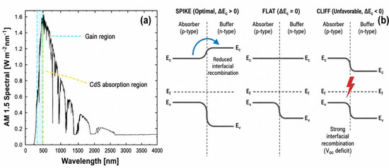
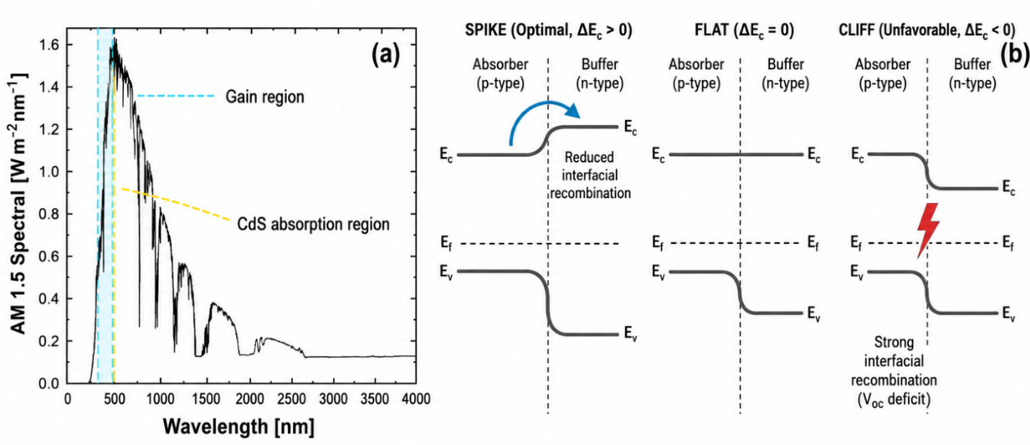
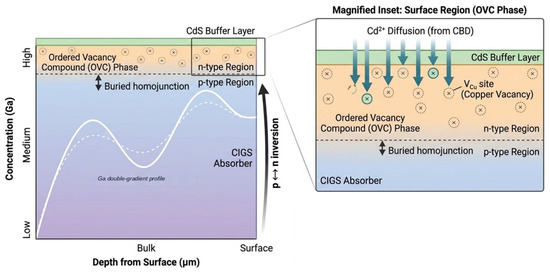
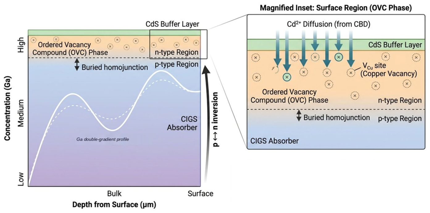
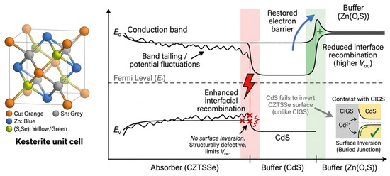
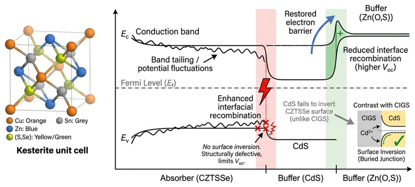
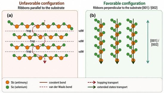
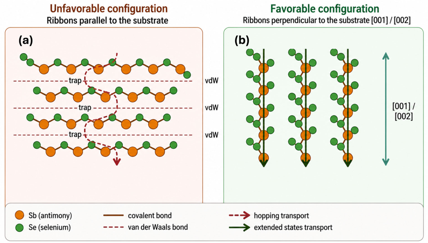
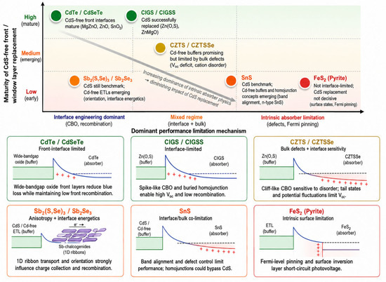
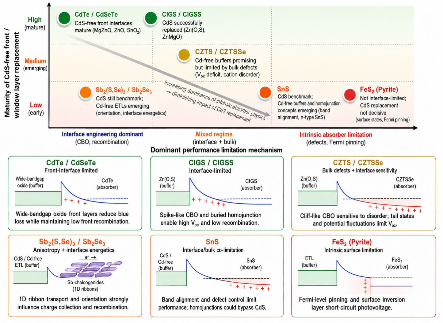

Disclaimer/Publisher’s Note: The statements, opinions and data contained in all publications are solely those of the individual author(s) and contributor(s) and not of MDPI and/or the editor(s). MDPI and/or the editor(s) disclaim responsibility for any injury to people or property resulting from any ideas, methods, instructions or products referred to in the content. |
© 2026 by the authors. Licensee MDPI, Basel, Switzerland. This article is an open access article distributed under the terms and conditions of the Creative Commons Attribution (CC BY) license.