Skip to Content

Nanomanufacturing

Nanomanufacturing is an international, peer-reviewed, open access journal on the fabrication of miniaturized devices or objects, their scalability, and their eventual industrial production, published quarterly online by MDPI.
  • Open Access— free for readers, with article processing charges (APC) paid by authors or their institutions.
  • Rapid Publication: manuscripts are peer-reviewed and a first decision is provided to authors approximately 39.3 days after submission; acceptance to publication is undertaken in 23.8 days (median values for papers published in this journal in the first half of 2026).
  • Recognition of Reviewers: Reviewers whose reports are timely and of high quality receive an APC discount voucher for a future publication in an MDPI journal. Become a reviewer.
  • Nanomanufacturing is a companion journal of Nanomaterials.

Get Alerted

Add your email address to receive forthcoming issues of this journal.

All Articles (118)

  • Feature Paper
  • Article
  • Open Access

Polypyrrole (PPy) nanofilms were deposited by in situ chemical oxidative polymerization on polyethylene or polypropylene. The thickness is determined by SEM of the cross-section. Thin thickness nanofilms (180 ± 5 nm) are deposited. The nanofilms are then modified by nucleophilic addition to attach functional groups to the nanofilms. Strong nucleophiles (e.g., thiols) react by conventional heating. Weak nucleophiles (e.g., nitroanilines) only react when applying microwaves. The spectroscopic (UV–visible, FTIR, XPS and XANES) characterization shows the attachment of functional groups and the change in electronic properties upon the reaction. The conductivity of the functionalized PPy nanofilms are lower than unmodified PPy nanofilms, likely due to steric effects on the extended conjugation and disturbance of the electron hopping between chains. While reaction with some nucleophiles (e.g., bisulfite ion) makes nanofilms more hydrophilic, modification with long alkyl chains or fluorinated long chains produces highly hydrophobic nanofilms. No noticeable effect of the reaction on the film thickness is observed, suggesting little or no loss of polymer due to dissolution.

Nanomanufacturing

9 September 2026

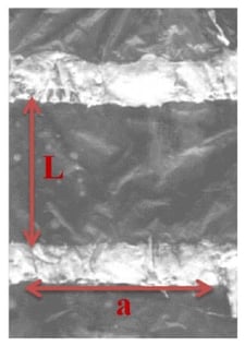
Photograph of PPy film on PE, with silver ink bands as electrical contacts.
  • Article
  • Open Access

A low-voltage alternating current (AC) field (20 V peak-to-peak, 1 kHz) was superimposed on a conventional direct current (DC) electrospinning configuration in order to test whether the shape of that perturbation measurably alters fiber formation. A function generator delivered sinusoidal, pulsed (square), ramp and arbitrary (noise) waveforms to a foil-covered flat collector, while a standard DC high-voltage source (20 kV) drove the jet from the spinneret. Polyvinylpyrrolidone (PVP) nanofibers were characterized by scanning electron microscopy (SEM), fiber-diameter distribution analysis (FIJI/ImageJ), quantitative orientation analysis and contact profilometry. One-way analysis of variance across the six conditions was significant (F(5.594) = 5.56, p = 5.1 × 10⁻⁵) but the associated effect size was small (η2 = 0.045). Relative to the connected control (237 ± 52 nm), the ramp (205.5 ± 43.9 nm), noise (201.3 ± 48.6 nm) and pulse (212.6 ± 70.0 nm) waveforms yielded significantly finer fibers (Tukey HSD, p = 0.0008, 0.0001 and 0.022, respectively); relative to the grounded control (215 ± 47 nm), no waveform reached significance. The ramp waveform produced the narrowest diameter distribution but, unexpectedly, the roughest mat of the four AC conditions (Ra = 1.95 µm against 0.74 µm for the grounded control), while the noise waveform gave both the smallest mean diameter and the smoothest mat (Ra = 0.61 µm); with a single profile per scan direction, these roughness values are descriptive rather than statistically compared. Quantitative orientation analysis using two independent estimators (structure tensor and fast Fourier transform) returned Herman orientation factors of S ≤ 0.13 for every condition, against S = 0.81 for a partially aligned reference population: no condition exceeded the isotropic noise floor of the FFT estimator (S95 = 0.141), and the three conditions that marginally exceeded the structure-tensor floor (S95 = 0.104) included the connected control, which received no oscillating signal. No waveform, including the pulsed waveform, produced fiber alignment attributable to the AC field. The applied AC amplitude corresponds to approximately 0.05% of the DC voltage, and the associated oscillating field (±50 V m−1) is approximately three orders of magnitude smaller than the mean DC field (~1 × 10⁵ V m−1); the electrohydrodynamic mechanisms discussed here are therefore presented as hypotheses requiring direct measurement rather than as established explanations. Within these limits, low-voltage waveform modulation is a simple, safe and retrofittable route to modest control of nanofiber diameter and mat uniformity in a single-polymer system, but it does not induce fiber alignment.

Nanomanufacturing

2 September 2026

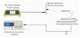
A combined experimental setup including the electrospinning under primary DC with a waveform generator as a secondary AC bias.
  • Feature Paper
  • Article
  • Open Access

We present a dual-wavelength analysis of nitrogen-vacancy (NV) center quantum magnetometry enhanced by uniformly coated gold nanoparticles (AuNPs). An ensemble-averaged model is developed to analyze the AuNP-enhanced stimulated absorption at the 532 nm excitation wavelength and the spontaneous emission at 637 nm. The resulting detected optically magnetic resonance (ODMR) signal profiles are simulated for both enhancement mechanisms. We find that the enhanced stimulated absorption at 532 nm significantly amplifies the ODMR signal intensity without broadening the linewidth, thereby improving the signal-to-noise ratio (SNR) without sacrificing the magnetic field sensing resolution. Conversely, enhancing the 637 nm spontaneous emission increases the total photo emission rate but simultaneously broadens the ODMR detection linewidth due to the direct reduction in the effective spin coherence time of excited states by the enhanced spontaneous rate. The dual-wavelength analysis provides valuable design guidance for the development of low-cost spin-coated AuNP-enhanced NV-center quantum magnetometry technologies.

Nanomanufacturing

1 September 2026

Energy level diagram of NV-center quantum magnetometry using the energy state symbol conventions given by Manson et al. [4]: (a) without external magnetic field; (b) under external magnetic field. The AuNPs can be selected to enhance the 532 nm optical excitation from the 
  
    
      A
      2


      3
    
  
 ground state (green arrows) or the 637 nm spontaneous emission (red and blue arrows) from the 
  
    
      E


      3
    
  
 excited state.
  • Article
  • Open Access

Historically, TEM prep has been an artisan craft without a systematic workflow that ensures quantified control over TEM sample thickness. Over- and under-thinning is a significant problem in the TEM prep process. A direct measurement process was demonstrated to control the final thickness of the TEM lamella. Final lamella thickness was controlled by directly measuring lamella thickness in real time using a 10–15 kV SEM while performing secondary electron imaging at the mill position, allowing for (human-mediated) closed-loop processing. We demonstrated the utility of this technique by systematically thinning five TEM samples to discretely target thicknesses ranging from 100 nm down to 28 nm. We demonstrated the repeatability and simplicity of the process by fabricating 10 STEM lamella with a targeted thickness of 32 nm. We demonstrate the ability to fabricate an engineered multi-layered structure that acts as a lamella thickness measurement feature that is independent of sample type, allowing a broader implementation of in-line lamella thickness monitoring. We applied our thickness measurement technique to three thin-film materials (Au, Ag, and Cu) to obtain TEM lamella thickness target values needed to achieve electron transparency for each material. Having knowledge of a target thickness parameter prevents the over- and under-thinning problem in TEM prep.

Nanomanufacturing

4 August 2026

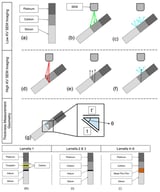
The figure illustrates the lamella film stack and the SE/BSE imaging process. The figure also shows the lamella composition for each phase. (a) shows protective platinum cap, carbon film, and silicon substrate. (b) shows the primary beam incident on lamella. (c) shows the SE captured for image formation. (d–f) shows the imaging process with high-energy SEM. (d) A high-energy SEM beam is incident on the sample with a large penetration depth. (e) BSE are generated from deep inside the sample. (f) BSE are converted into SE at the surface of the lamella and used to generate the image. (g) shows the relationship between the observed thickness t’ and the real thickness t, t’ = t × cos(θ). Theta θ is 52° at the neutral mill position. (h) Lamella 1 was composed of a platinum cap, tungsten layer, iridium layer, silicon substrate, and two carbon layers surrounding the tungsten layer. (i) Lamella 2–3 were composed of a platinum cap, carbon layer, iridium layer, and silicon substrate. (j) Lamella 4–6 were composed of a platinum cap, carbon layer, thin-film metal, and substrate (silicon or SiO2).

Highly Accessed Articles

News & Conferences

Latest Issues

Open for Submission

Journal Sections

XFacebookLinkedIn
Nanomanufacturing - ISSN 2673-687X