


Abstract
The formation of carbon nanostructures and silicon carbide (SiC) using a single-source precursor offers a simplified route for material synthesis; however, the factors governing the transition between CNT-like structure formation and SiC growth remain unclear. In this study, the growth behavior of carbon-related structures using vinylsilane was systematically investigated by hot-wall chemical vapor deposition (CVD) on various substrates, including Fe bulk substrates and Fe thin films on SiO2/Si. CNT-like structures were preferentially formed on Fe bulk substrates, whereas Fe thin-film substrates exhibited CNT-like growth at the initial stage followed by increased Si–C-related phase formation with increasing growth temperature and growth time. In contrast, on Fe thin films with limited catalyst amounts, CNT-like growth occurred initially, followed by increased Si–C-related phase formation with increasing growth temperature and growth time. These observations are consistent with a growth transition associated with the balance between Si uptake into the metal and surface SiC formation processes. By controlling catalyst amount, growth temperature, and growth time, the relative formation of CNT-like structures, SiC-rich coatings, and intermediate morphologies could be tuned within a single process. Furthermore, a SiC/CNT-like composite structure was directly formed on a conductive Fe substrate in a one-step CVD process. Electrochemical measurements showed an enhanced current response compared with a bare Fe substrate, indicating preliminary electrochemical activity and suggesting potential applicability as a high-surface-area electrode platform.
1. Introduction
Silicon carbide (SiC) is an attractive material owing to its wide bandgap, high mechanical robustness, and excellent chemical and thermal stability, and has attracted considerable attention as a functional thin-film and coating material across a wide range of fields. In recent years, comprehensive reviews on SiC thin-film technologies, deposition processes, and functional coating applications have been reported, providing a systematic understanding of its material properties and application potential [1]. Based on these characteristics, SiC has been extensively investigated for applications such as protective coatings on metal surfaces [2,3,4], corrosion-resistant layers under harsh environments, and electrode materials and coatings for electrochemical energy conversion systems, including photoelectrodes [5].
Electrochemical energy conversion reactions are particularly sensitive not only to intrinsic material properties but also to the surface structural design of electrodes, which strongly influences reaction efficiency. In water-splitting reactions, mass transport at the reaction interface and the behavior of generated gas bubbles are directly linked to device performance. Therefore, controlling electrode surface morphology has become an important challenge for improving electrochemical reaction efficiency. The introduction of three-dimensional (3D) nanostructures with surface roughness is widely recognized as an effective strategy to enhance electrode performance.
One effective approach to constructing such 3D nanostructures is to utilize carbon nanotubes (CNTs) [6,7,8] as structural templates in combination with functional materials. CNTs possess a high aspect ratio, excellent electrical conductivity, and mechanical flexibility, enabling the formation of porous and compliant architectures. However, CNTs tend to aggregate due to strong van der Waals interactions, which reduces the accessible surface area and increases resistance within the CNT network, thereby deteriorating electrochemical performance. To overcome this limitation, CNTs are often integrated with other materials to form hybrid structures with improved electrical connectivity and enhanced electrochemically active surfaces. Such CNT-based composites, including TiO2/CNT, ZnO/CNT, Fe2O3/CNT, and CuWO4/CNT hybrid structures, have been widely explored as platforms for functional coatings and electrochemical applications, including photoelectrochemical systems [9].
SiC is also a promising candidate for electrode and photoelectrode applications owing to its wide bandgap and excellent chemical stability, and its application to photoelectrochemical water splitting has been reported [5,10,11,12,13]. Combining SiC with CNT-based 3D architectures is therefore expected to integrate the chemical stability and electrochemical functionality of SiC with the high surface area and conductive network provided by CNTs, thereby facilitating charge transport and interfacial reactions. CNT-based composites, including SiC/CNT structures, have been investigated for mechanical reinforcement, thermal property control, and surface functionalization [14,15,16,17]. However, most reported SiC/CNT structures are fabricated through multistep processes, where CNTs are first synthesized and subsequently coated with SiC. Such approaches increase fabrication complexity and often require CNT dispersion, surface modification, and high-temperature processing, which may cause CNT agglomeration, nanotube damage, and poor interfacial load transfer. In addition, CNT growth and subsequent SiC coating are typically conducted in separate processing steps, resulting in longer and more complicated fabrication procedures. Therefore, the development of a single-step or continuous growth approach remains an important challenge.
In general, CNT growth requires transition-metal catalysts such as Fe, Ni, or Co together with hydrocarbon precursor gases including ethylene or acetylene [6,7,8]. In contrast, a single-source precursor capable of supplying both carbon and silicon species offers the possibility of simultaneously forming CNT-like structures and SiC within a single process. The growth behavior of carbon-related structures and SiC under such conditions has not been systematically investigated on metal substrates.
In this study, we focus on vinylsilane as a single-source precursor for both carbon-related structure formation and SiC growth. The presence of a Si–C bond enables SiC formation using vinylsilane alone as the precursor. Previous studies have demonstrated that vinylsilane is an effective precursor for SiC deposition over a wide temperature range, including SiC film growth on Si substrates at 600–1000 °C and deposition on Cu substrates at temperatures as low as 700 °C [18]. Epitaxial growth of 3C-SiC on Si substrates has also been demonstrated using vinylsilane [19]. In addition, SiC deposition on carbon nanowalls (CNWs) has been reported, indicating that vinylsilane can be applied not only to conventional substrates but also to nanostructured carbon materials [20].
Vinylsilane also contains a vinyl group with a molecular structure similar to ethylene, a widely used carbon source for catalytic CNT growth. Therefore, thermal decomposition of vinylsilane can potentially provide carbon species for filamentous carbon growth, while the Si–C bond serves as a source of silicon-containing species for SiC formation. Consequently, competition between carbon nanostructure formation and SiC growth may occur depending on catalyst characteristics, substrate configuration, and growth conditions. However, despite these previous studies, the factors governing the transition between CNT-like structure formation and SiC formation in a single-step vinylsilane process remain poorly understood.
Accordingly, this study investigates the growth behavior of carbon-related structures and SiC films using vinylsilane as a single-source precursor on various metal substrates, aiming to clarify the factors governing the transition between CNT-like structure formation and SiC formation.
2. Materials and Methods
Thin metal films were deposited on Si (100) substrates (resistivity ≤ 0.01 Ω·cm) coated with a thermally grown SiO2 layer (thickness: 500 nm ± 10%) by a resistance-heating evaporation system. Ti, Fe, Co, and Ni were used as metal thin films, and their thicknesses were 33 nm (Ti), 60 nm (Fe), 45 nm (Co), and 47 nm (Ni), respectively. For comparison, bulk metal substrates of Ti, Fe, Co, and Ni were also used.
Growth experiments were carried out by hot-wall chemical vapor deposition (CVD) using vinylsilane as a single-source precursor and Ar as a carrier gas. The substrates used in this study consisted of metal thin film substrates (Ti/SiO2/Si, Fe/SiO2/Si, Co/SiO2/Si, and Ni/SiO2/Si), bare SiO2/Si substrates, and bulk metal substrates (Ti, Fe, Co, and Ni). The growth time was typically fixed at 60 min. To investigate time-dependent growth behavior, additional experiments were conducted on Fe thin-film substrates (Fe/SiO2/Si) with growth times of 15 and 120 min at 850 °C.
The deposition conditions used in this study are summarized in Table 1. For bulk metal substrates, the vinylsilane flow rate and growth pressure were set to 6 sccm and 1 Torr, respectively. In contrast, for metal thin film substrates and bare SiO2/Si substrates, they were set to 4 sccm and 2 Torr, respectively. The growth temperature was varied in the range of 750 and 950 °C depending on the substrate and experimental purpose, while 850 °C was used for time-dependent experiments. As summarized in Table 1, different precursor flow rates and pressures were employed for bulk metal substrates and metal thin-film substrates. These conditions were selected to enable meaningful comparison of growth behavior among different substrate types. Prior to deposition, all substrates were subjected to hydrogen pretreatment at the corresponding deposition temperature with a hydrogen flow rate of 150 sccm for 10 min to remove surface contaminants.
Table 1.
Summary of deposition conditions used for bulk metal substrates and metal thin-film substrates (Metal/SiO2/Si).
After deposition, the samples were characterized to analyze the reactions between the metals and the precursor. Surface and cross-sectional morphologies, as well as film thicknesses, were examined using scanning electron microscopy (SEM; JSM-6700F, JEOL Ltd., Tokyo, Japan). Surface bonding states and elemental composition ratios were analyzed by Raman spectroscopy (RAMAN-11, Nanophoton Corporation, Osaka, Japan) using a 532 nm excitation laser and X-ray photoelectron spectroscopy (XPS; ESCALAB250, VG Scientific, East Grinstead, UK). The crystalline structures of the deposited films were evaluated by X-ray diffraction (XRD; Rigaku RINT2100, Rigaku Corporation, Tokyo, Japan) using a Cu Kα X-ray source. UV Raman spectroscopy was performed using an NRS-5100PL system (JASCO Corporation, Tokyo, Japan). Transmission electron microscopy (TEM) observations were performed using a JEM-2100PLUS microscope (JEOL Ltd., Tokyo, Japan). Cyclic voltammetry measurements were performed using an HZ-7000 electrochemical measurement system (Hokuto Denko Corporation, Tokyo, Japan).
3. Results
3.1. Growth Using Vinylsilane on Bulk-Metal Substrates
Raman Analysis of Carbon Bonding on Catalytic and Non-Catalytic Substrates
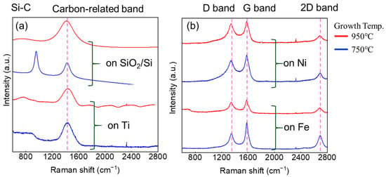
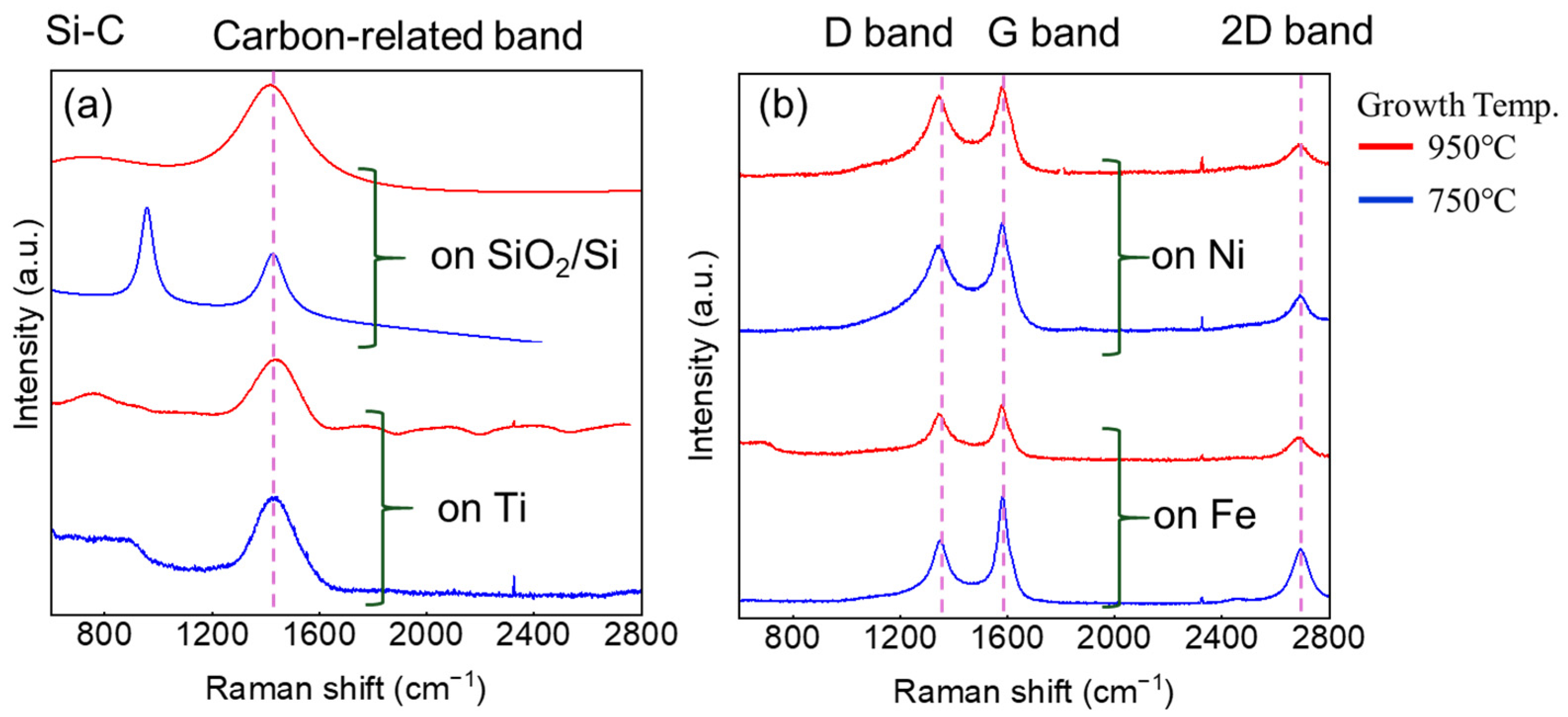
To confirm the formation of carbon-related structures, Raman spectroscopy was performed for samples grown on Ti, Ni, and Fe metal substrates as well as on SiO2/Si substrates at growth temperatures of 750 °C and 950 °C for 60 min using vinylsilane as a precursor. The obtained Raman spectra are shown in Figure 1a,b.
Figure 1.
Raman spectra of samples grown using vinylsilane for 60 min at 750 °C and 950 °C on (a) non-catalytic substrates (SiO2/Si and Ti) and (b) catalytic metal substrates (Ni and Fe). Dashed lines are guides to the eye indicating the approximate positions of the characteristic Raman bands.3.1.2. SEM Observation of Surface Morphology.
As shown in Figure 1a, for samples grown on non-catalytic substrates (SiO2/Si and Ti), the SiO2/Si and Ti samples grown at 950 °C exhibited a broad Raman band centered around ~800 cm−1. This feature is attributed to Si–C bonding associated with SiC. In crystalline 3C-SiC, the transverse optical (TO) and longitudinal optical (LO) phonon modes appear at ~795–796 cm−1 and ~972 cm−1, respectively [21,22,23]. In polycrystalline or amorphous SiC, however, these peaks broaden and overlap, appearing as a broad Si–C (TO/LO) band in the 600–1000 cm−1 region [3,21,22,23]. Therefore, the observed broad band near 800 cm−1 indicates the formation of SiC-related phases on the SiO2/Si and Ti substrates. In addition, a broad Raman feature was observed around ~1420 cm−1 at both 750 °C and 950 °C. Similar bands around ~1420 cm−1 have been reported for carbon-rich amorphous SiC and are attributed to C–C bonding incorporated into a disordered Si–C network [24,25]. This behavior differs from disordered carbon, which typically exhibits a D band near ~1350 cm−1 and a G band in the ~1500–1630 cm−1 range [26]. Accordingly, the ~1420 cm−1 feature is attributed to carbon-related bonding associated with carbon-rich Si–C materials rather than graphitic carbon or CNT structures.
In contrast, for samples grown on catalytic metal substrates (Figure 1b), three prominent Raman bands were observed at approximately 1350, 1580, and 2700 cm−1 at both 750 °C and 950 °C. These correspond to the D, G, and 2D bands of sp2-bonded graphitic carbon, including CNT-related structures [27,28,29,30,31]. The G band (~1580 cm−1) arises from the in-plane optical phonon mode (E2g) of the sp2 lattice [27,28,29,30,31], while the 2D band (~2700 cm−1) is a second-order feature associated with a double-resonance process [27,31]. The D band (~1350 cm−1) is activated by structural disorder in the sp2 network [27,28,29,31]. Compared with the non-catalytic substrates, the Raman spectra of the catalytic metal substrates were dominated by graphitic carbon signals, and no distinct Si–C-related Raman feature was observed near ~800 cm−1 under the present conditions.
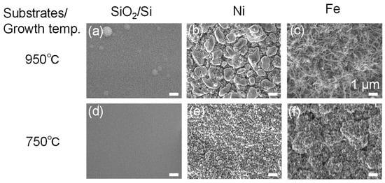
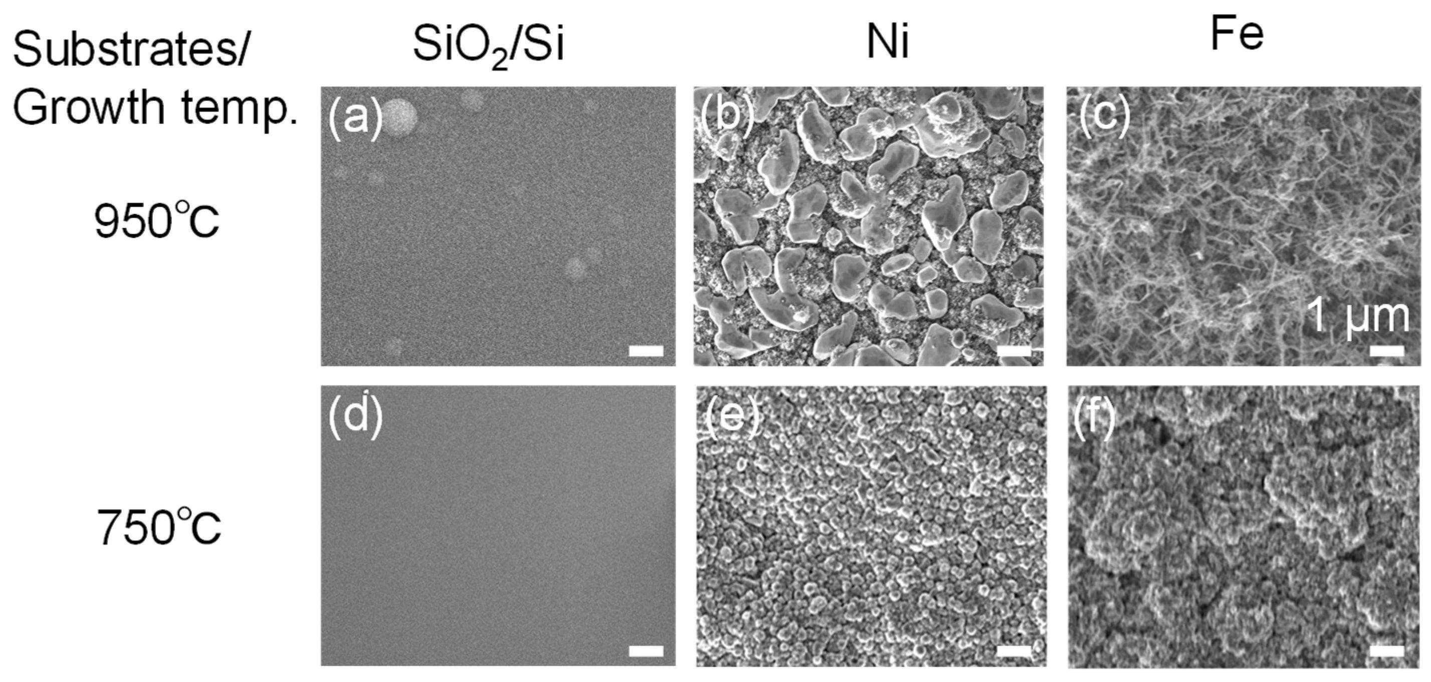
To examine the morphology of the formed structures depending on the substrate type, SEM observations were carried out. Figure 2a–f show surface SEM images of samples grown on SiO2/Si, Ni, and Fe substrates at growth temperatures of 750 °C and 950 °C.
Figure 2.
Surface SEM images of samples grown using vinylsilane on (a,d) SiO2/Si, (b,e) Ni, and (c,f) Fe substrates at (a–c) 950 °C and (d–f) 750 °C. All scale bars correspond to 1 μm.
Figure 2a and Figure 2d show the surface morphologies of samples grown on SiO2/Si substrates at 950 °C and 750 °C, respectively. The film grown at 750 °C exhibited a smooth surface, suggesting that the deposition process mainly proceeded via surface reactions. In contrast, at 950 °C, spherical particles with various sizes appeared. Accordingly, the discussion was revised to indicate that the particles may be associated with particulate by-products generated within the hot-wall reactor, while their exact origin remains unclear. Figure 2b,e show the surface morphologies of samples grown on Ni substrates. At both temperatures, granular structures distinct from those on SiO2/Si were observed, and the particle size increased with increasing growth temperature. The average Feret diameter estimated from SEM images increased from 0.39 ± 0.11 µm at 750 °C (n = 60) to 1.50 ± 0.55 µm at 950 °C (n = 39), indicating significant particle coarsening at elevated temperatures. Combined with the Raman results indicating graphitic carbon formation, these structures are likely associated with reactions between vinylsilane and Ni.
Figure 2c,f show the surface morphologies of samples grown on Fe substrates. At 750 °C, a rough surface with irregular features was observed, whereas at 950 °C, thin filamentous structures were observed. Based on the combined results of Raman spectroscopy and SEM observations, these structures are considered to be CNT-like filamentous structures. Hereafter, these structures are referred to as CNT-like structures.
These results demonstrate that the morphology of the deposited structures strongly depends on the substrate type. In particular, Si–C-related phases were preferentially observed on non-catalytic substrates, whereas graphitic carbon structures, including CNT-like morphologies, were preferentially formed on catalytic metal substrates. At elevated temperatures (950 °C), Fe substrates tended to produce high-surface-area filamentous structures, suggesting that the formation of Si–C-related phases or carbon nanostructures is influenced by substrate selection.
3.2. Growth on Metal Thin-Films/SiO2/Si Using Vinylsilane
To further investigate the factors governing CNT-like structure formation and SiC growth, growth experiments were conducted using metal thin-film substrates.
3.2.1. Raman Analysis on Metal Thin-Films/SiO2/Si
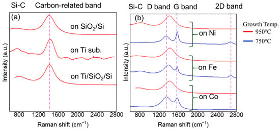
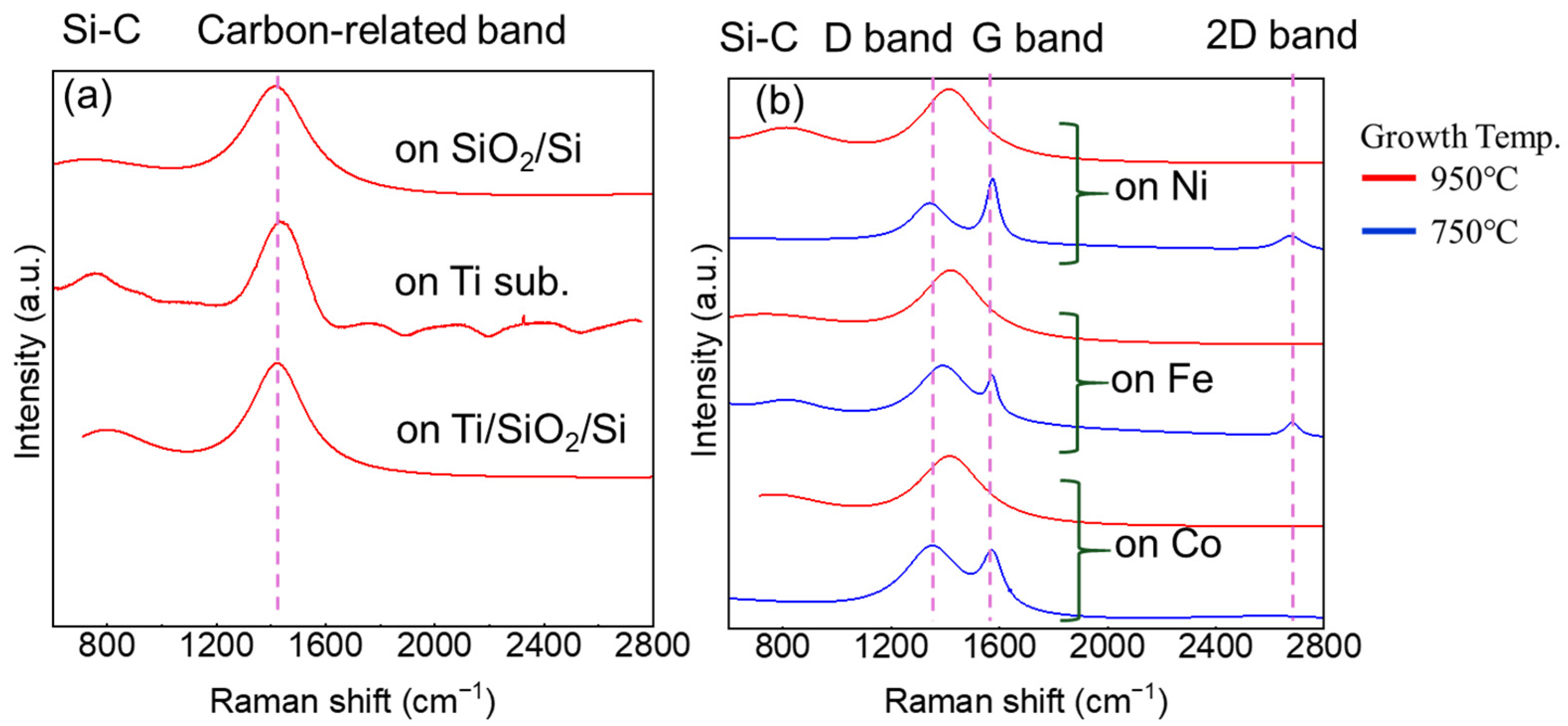
Figure 3a,b show the Raman spectra of samples grown on metal thin-film substrates. Figure 3a compares samples grown on non-catalytic Ti thin-film, Ti bulk, and SiO2/Si substrates at 950 °C to evaluate the influence of the Ti substrate configuration on the resulting bonding characteristics. The Raman spectra of the Ti bulk and SiO2/Si substrates were previously shown in Figure 1 and are included again here for direct comparison. Figure 3b shows the spectra of samples grown on catalytic metal thin films (Ni, Fe, and Co) at 750 °C and 950 °C for a fixed growth time of 60 min.
Figure 3.
Raman spectra of samples grown using vinylsilane on metal thin film substrates. (a) Comparison of Raman spectra obtained from Ti thin-film, Ti bulk, and SiO2/Si substrates grown at 950 °C. (b) Catalytic metal thin films (Fe, Ni, and Co) grown at 750 °C and 950 °C for 60 min. Dashed lines are guides to the eye indicating the approximate positions of the characteristic Raman bands.
As shown in Figure 3a, the samples grown on Ti thin films exhibit a broad Si–C-related band centered around ~800 cm−1 together with a broad carbon-related band at ~1420 cm−1. These features are consistent with those observed on Ti bulk and SiO2/Si substrates under the same conditions, indicating similar bonding characteristics regardless of the Ti substrate configuration.
Figure 3b shows the Raman spectra of samples grown on Fe, Ni, and Co thin film substrates. At 750 °C, the D and G bands are observed for all metal thin films, and the 2D band is additionally detected for Fe and Ni, indicating the formation of sp2-bonded graphitic carbon (CNT-like) structures. For the Fe thin film, a Si–C-related feature around ~800 cm−1 is also observed, suggesting the coexistence of SiC-related bonding and graphitic carbon. In contrast, when the growth temperature is increased to 950 °C, the D, G, and 2D bands disappear, and the spectra are dominated by the Si–C-related band (~800 cm−1) together with the broad band at ~1420 cm−1. This result indicates that Si–C-related bonding becomes dominant in the Raman response under these conditions.
To provide a more quantitative comparison of the Raman features, peak-fitting analysis was performed. The resulting peak positions, full width at half maximum (FWHM) values, and intensity ratios (IG/ID and I2D/IG) are summarized in Table S1 of the Supplementary Information. For the Fe bulk substrate, well-resolved D, G, and 2D bands were observed at both temperatures, with IG/ID values of 0.99 and 0.79 at 750 and 950 °C, respectively. In contrast, the Fe thin-film substrate exhibited a much lower IG/ID value (0.17) at 750 °C, while the distinct D, G, and 2D bands were no longer resolved at 950 °C and were replaced by a broad carbon-related band centered at 1424.8 cm−1. This peak position is close to those observed for the SiO2/Si, Ti bulk, and Ti thin-film samples, which exhibited broad carbon-related bands at approximately 1420–1437 cm−1. These results suggest that the relative contributions of graphitic carbon and Si–C-related bonding depend strongly on the growth conditions used for the metal thin-film substrates.
3.2.2. SEM Observation of Surface Morphology on Metal Thin-Films/SiO2/Si
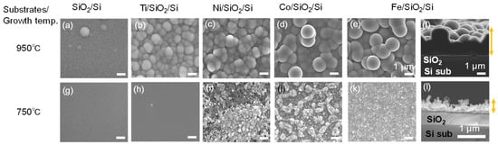
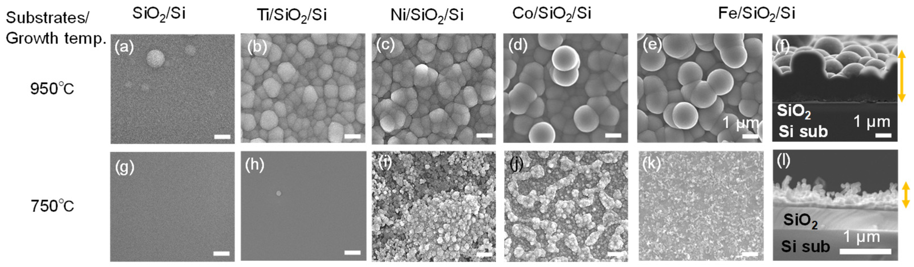
Figure 4a–e,g–k show surface SEM images of structures formed on Ti/SiO2/Si, Ni/SiO2/Si, Co/SiO2/Si, and Fe/SiO2/Si using vinylsilane for 60 min at growth temperatures of 750 °C and 950 °C. The SiO2/Si data shown in Figure 4a,g were previously presented in Figure 2 and are included again here to facilitate direct comparison with the metal thin-film substrates. Figure 4f and Figure 4l show cross-sectional SEM images of Fe thin films corresponding to the surface morphologies shown in Figure 4e and Figure 4k, respectively.
Figure 4.
Surface and cross-sectional SEM images of metal thin films after growth using vinylsilane for 60 min. (a–e) Surface SEM images of Ti, Ni, Co, and Fe thin films grown at 950 °C, and (f) the corresponding cross-sectional image of (e). (g–k) Surface SEM images of Ti, Ni, Co, and Fe thin films grown at 750 °C, and (l) the corresponding cross-sectional image of (k). All scale bars correspond to 1 μm. The arrows indicate the approximate height of the grown structures.
At 750 °C, the non-catalytic Ti thin film exhibited a smooth surface similar to that observed on SiO2 substrates, whereas granular structures were formed on the catalytic metal thin films (Ni, Co, and Fe). The surface morphology strongly depended on the metal species, with the finest structures observed on the Fe thin film. A cross-sectional SEM image of the Fe thin film (Figure 4l) reveals filamentous structures with heights of approximately 500–800 nm. Based on the combined results of SEM observations and Raman spectroscopy, these structures are considered to be CNT-like filamentous structures.
In contrast, at 950 °C, the surface morphology changed significantly. Irregular granular morphologies were observed on Ti and Ni thin films, whereas spherical surface structures were observed on Co and Fe thin films. In particular, spherical particles with diameters of approximately 1.5 μm were formed on the Co and Fe thin films, similar to those observed on SiO2 substrates. Cross-sectional SEM observations of the Fe/SiO2/Si thin-film sample show that the film thickness increased to approximately 1.5–3 μm, with a hemispherical surface morphology. Compared with the samples grown at 750 °C, both the particle diameter and film thickness increased, indicating enhanced film growth under the 950 °C condition.
Although differences in surface morphology were observed depending on the metal species, all samples exhibited grain-like structures at 950 °C, and the Raman spectra showed similar overall trends. These results suggest that Si–C-related phases become dominant under these conditions, resulting in the formation of films containing amorphous carbon components. These observations are consistent with the Raman results, suggesting that the relative contributions of graphitic carbon and Si–C-related bonding vary depending on the growth conditions.
3.2.3. X-Ray Diffraction Analysis of SiC Formation on Metal Thin-Film Substrates
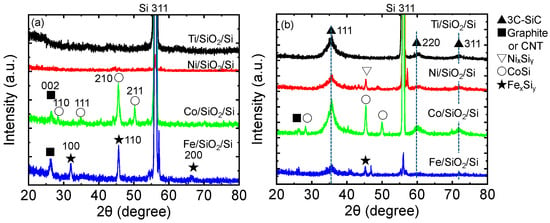
Figure 5a and Figure 5b show the X-ray diffraction (XRD) patterns of Ti/SiO2/Si, Ni/SiO2/Si, Co/SiO2/Si, and Fe/SiO2/Si thin-film substrates after growth using vinylsilane at growth temperatures of 750 °C and 950 °C, respectively.
Figure 5.
X-ray diffraction (XRD) patterns of metal thin film substrates after growth using vinylsilane at (a) 750 °C and (b) 950 °C. The substrates are Ti/SiO2/Si, Ni/SiO2/Si, Co/SiO2/Si, and Fe/SiO2/Si. Measurements were performed using Cu Kα radiation.
For the samples grown at 750 °C (Figure 5a), only the Si (331) diffraction peak from the Si substrate at approximately 56° was observed for samples grown on Ti/SiO2/Si and Ni/SiO2/Si thin-film substrates, and no distinct peaks attributable to the deposited layers, silicide phases, or carbon-related structures were detected. This may indicate that the deposited layers were either too thin, poorly crystalline, or below the detection limit of the present XRD measurement.
In contrast, the Co/SiO2/Si and Fe/SiO2/Si thin-film substrates exhibit multiple diffraction peaks, including a peak at approximately 2θ ≈ 26–27°, which corresponds to the (002) reflection of graphitic carbon commonly observed in graphitic or turbostratic carbon structures, including CNT-like materials [32,33,34,35]. In addition, several peaks can be assigned to Co–Si [36] and Fe–Si [37,38] silicide phases, suggesting that Si species supplied from vinylsilane may react with the metal layers to form silicides under these growth conditions.
For the samples grown at 950 °C (Figure 5b), an additional diffraction peak appears at approximately 2θ ≈ 36° for all metal thin-film substrates. This peak can be assigned to the 3C-SiC (111) reflection [38,39], suggesting the formation of SiC-related phases on all metal thin-film substrates at elevated temperatures. However, contributions from overlapping diffraction features originating from structurally disordered carbon phases cannot be completely excluded based solely on XRD analysis. Furthermore, for the Ti, Ni, and Co thin-film substrates, additional peaks at approximately 2θ ≈ 60° and 72° are observed, corresponding to the 3C-SiC (220) and (311) reflections, respectively [39,40], consistent with the formation of polycrystalline SiC. For the Fe thin-film substrate, the high-angle SiC-related reflections were not clearly resolved. Although SiC-related diffraction was observed at lower angles, the origin of the weaker diffraction intensity at higher angles could not be determined from the present XRD data alone.
Furthermore, silicide-related diffraction peaks were observed for the Co and Fe thin-film substrates at 950 °C. In addition to the SiC-related reflections, silicide-related diffraction peaks were observed for the Co, Fe, and Ni thin-film substrates at 950 °C. The diffraction features observed for the Ni/SiO2/Si thin-film substrate can be attributed to nickel silicide phases (NixSiγ) [41]. In contrast, no peaks attributable to metal silicides were observed for the Ti/SiO2/Si thin-film substrate, where only SiC-related reflections were detected in addition to the Si substrate peak. These diffraction features are consistent with silicide formation on catalytic metal thin-film substrates under high-temperature growth conditions.
The SEM, Raman, and XRD results revealed clear differences in morphology, bonding characteristics, and phase formation between the Fe bulk and Fe/SiO2/Si thin-film substrates. To further investigate the bonding states associated with these distinct growth behaviors, XPS measurements were performed.
3.2.4. XPS Analysis of Surface Bonding States on Fe Bulk Substrates and Fe/SiO2/Si Thin-Film Substrates
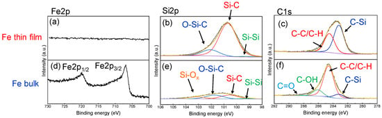
Figure 6a–f show the XPS spectra of the surfaces of samples grown on Fe thin-film substrates and Fe bulk substrates, respectively, after growth at 950 °C.
Figure 6.
XPS spectra of samples grown using vinylsilane at 950 °C. (a–c) Fe thin film and (d–f) Fe bulk substrates. (a,d) Fe 2p, (b,e) Si 2p, and (c,f) C 1s core-level spectra. Deconvoluted peak components are shown.
Figure 6a and Figure 6d present the Fe 2p spectra of the samples grown on the Fe thin film and the Fe bulk substrate, respectively. For the sample grown on the Fe bulk substrate, distinct Fe 2p peaks were clearly observed, whereas these peaks were hardly detected for the sample grown on the Fe thin film. This result indicates that a sufficiently thick overlayer was formed on the Fe thin film, such that the underlying Fe is located beyond the XPS detection depth. Although the overlayer thickness was not quantitatively evaluated, the absence of a detectable Fe 2p signal suggests that the overlayer formed on the Fe thin-film substrate exceeds the effective XPS detection depth.
Figure 6b and Figure 6e show the Si 2p spectra of the samples grown on the Fe thin film and the Fe bulk substrate, respectively. Based on reported peak components and binding-energy assignments for SiC-based films, the Si 2p spectrum of the Fe thin film sample was deconvoluted into three components corresponding to Si–Si/Si–H, Si–C, and O–Si–C bonds [42]. In contrast, the Si 2p spectrum of the Fe bulk substrate sample was fitted using four components, including an additional Si–Ox component, following the same literature-based assignments [42]. As a result, the Si–C bonding component is dominant for the Fe thin film, whereas comparable contributions from O–Si–C and Si–C components are observed for the Fe bulk substrate.
Figure 6c and Figure 6f show the C 1s spectra of the samples grown on the Fe thin film and the Fe bulk substrate, respectively. The C 1s spectra were deconvoluted into C–Si, C–C/C–H, C–O–H, and C=O components based on reported XPS analyses and assignments [42]. For the sample grown on the Fe thin film, dominant Si–C (C–Si) and C–C/C–H bonding components are observed. In contrast, the sample grown on the Fe bulk substrate exhibits a dominant C–C/C–H component, together with weaker Si–C (C–Si), C–O–H, and C=O components.
These results indicate that Si–C bonding is clearly observed on the Fe thin-film surface, whereas C–C/C–H bonding remains dominant on the Fe bulk substrate surface. To provide a more quantitative comparison of the XPS results, the fitted binding energies, full width at half maximum (FWHM) values, and relative component areas are summarized in Table S2 of the Supplementary Information. The fitting results show that the relative Si–C component area within the Si 2p spectrum is substantially larger for the Fe thin-film substrate (64.5%) than for the Fe bulk substrate (30.4%). Likewise, the relative C–Si component area within the C 1s spectrum is higher for the Fe thin-film substrate (58.9%) than for the Fe bulk substrate (9.7%). These values represent relative component areas within each core-level spectrum and do not correspond to elemental atomic concentrations. Considering the Fe 2p, Si 2p, and C 1s spectra together, these differences can be interpreted as being consistent with differences in the Si uptake behavior of the substrates. In the Fe thin-film substrate, the limited Fe volume may restrict further diffusion of Si into the metal layer, which could contribute to the accumulation of Si-containing species near the surface and consequently a stronger Si–C contribution. In contrast, in the Fe bulk substrate, Si species may diffuse further into the substrate, which could reduce the relative amount of surface Si–C species and result in a more carbon-rich surface composition. These observations are consistent with the proposed interpretation that competition between Si diffusion/uptake and surface Si–C formation influences the observed bonding states.
3.3. Effect of Growth Time on CNT-like Structure Formation
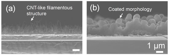
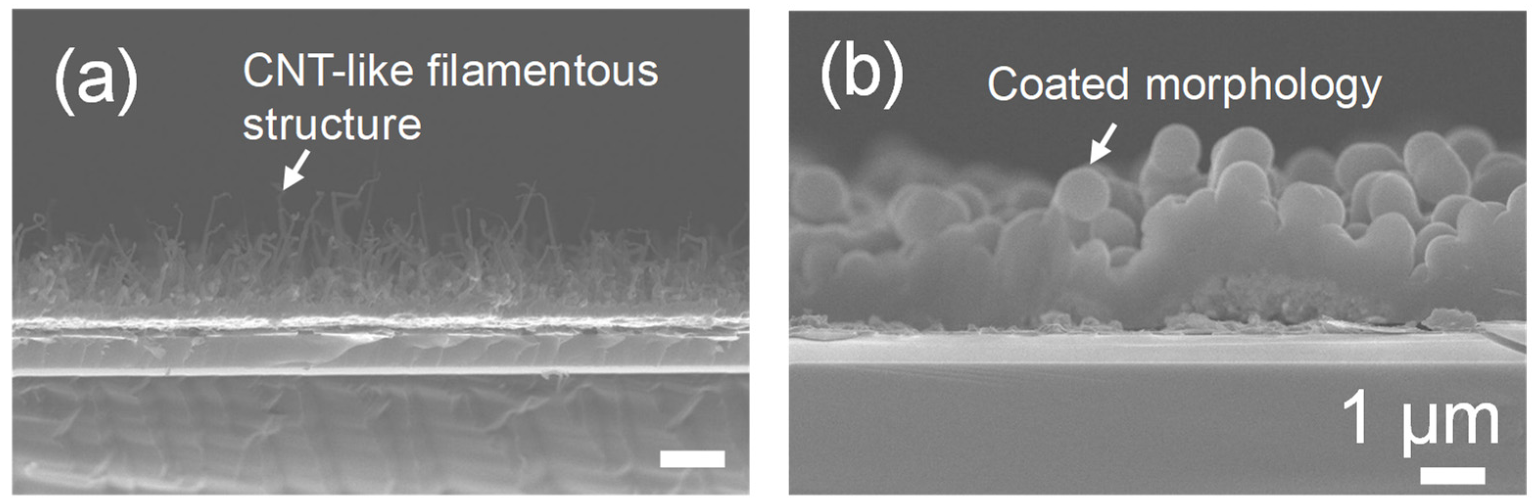
To clarify the time-dependent evolution of CNT-like structures formed using vinylsilane, growth experiments were carried out at a fixed temperature of 850 °C for different growth times. The temperature of 850 °C was selected as an intermediate condition between the CNT-like morphology observed at 750 °C and the coated morphology observed at 950 °C. Growth times of 15 min and 120 min were chosen to represent the early and advanced stages of growth, respectively, while 60 min served as an intermediate condition. While the temperature-dependent results described above suggest a transition from CNT-like filamentous morphologies to coated morphologies on metal thin-film substrates, time-dependent experiments were conducted to examine how the growth behavior changes during the deposition process. Figure 7a and Figure 7b show cross-sectional SEM images of Fe/SiO2/Si substrates grown for 15 and 120 min, respectively.
Figure 7.
Cross-sectional SEM images of structures grown at 850 °C for (a) 15 min and (b) 120 min on Fe/SiO2/Si substrates using vinylsilane. Scale bar: 1 µm.
After a growth time of 15 min (Figure 7a), high-aspect-ratio filamentous structures were observed to extend to lengths of approximately 1–2 μm. These structures are similar in morphology to those observed on Fe bulk substrates, suggesting that filamentous growth proceeds preferentially at the initial stage under these conditions. The relatively small diameter and high aspect ratio suggest that vertical growth is dominant during the early growth period. In contrast, after a growth time of 120 min (Figure 7b), the overall height of the structures increased only slightly to approximately 2–3 μm, while the diameter increased significantly. The tips of the structures exhibited hemispherical morphologies with diameters of approximately 700 nm. Although a height of about 2 μm was already achieved after 15 min, prolonged growth mainly resulted in lateral thickening rather than further vertical elongation. These observations indicate a clear transition in the growth mode with increasing growth time. The filamentous structures initially grow vertically with a small diameter. However, with prolonged growth, the overall height increases only slightly, whereas the structure diameter increases substantially. This behavior suggests that the growth mode changes with increasing growth time. While filamentous structures dominate after 15 min, prolonged growth leads to substantial thickening of the deposited layer and the appearance of a coated morphology. The morphology observed after 120 min no longer resembles an exposed filamentous structure and instead appears as a coated morphology.
Therefore, the time-dependent evolution observed in this study suggests that growth time plays a critical role in determining the final morphology. Short growth times are associated with high-aspect-ratio filamentous structures, whereas prolonged growth results in a coated morphology rather than high-aspect-ratio filamentous structures. The exposed filamentous morphology obtained at shorter growth times provides a higher-aspect-ratio structure and a more accessible surface than the coated morphology observed after prolonged growth. By controlling the growth duration, it is possible to tune the balance between these two morphologies depending on the intended application.
3.4. Electrochemical Applicability of the SiC/CNT-like/Fe Bulk Structure
To evaluate the electrochemical applicability of the structure, a SiC/CNT-like composite structure was directly fabricated on a conductive Fe bulk substrate under optimized growth conditions. This structure is hereafter referred to as the SiC/CNT-like/Fe sample. Fe was selected because it exhibited the most pronounced filamentous morphology among the investigated substrates and therefore provided the most suitable representative system for evaluating the electrochemical behavior of the deposited SiC/CNT-like composite structure. Growth was carried out on the Fe bulk substrate at 850 °C for 1 h using vinylsilane (2 sccm).
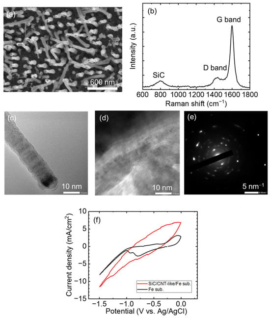
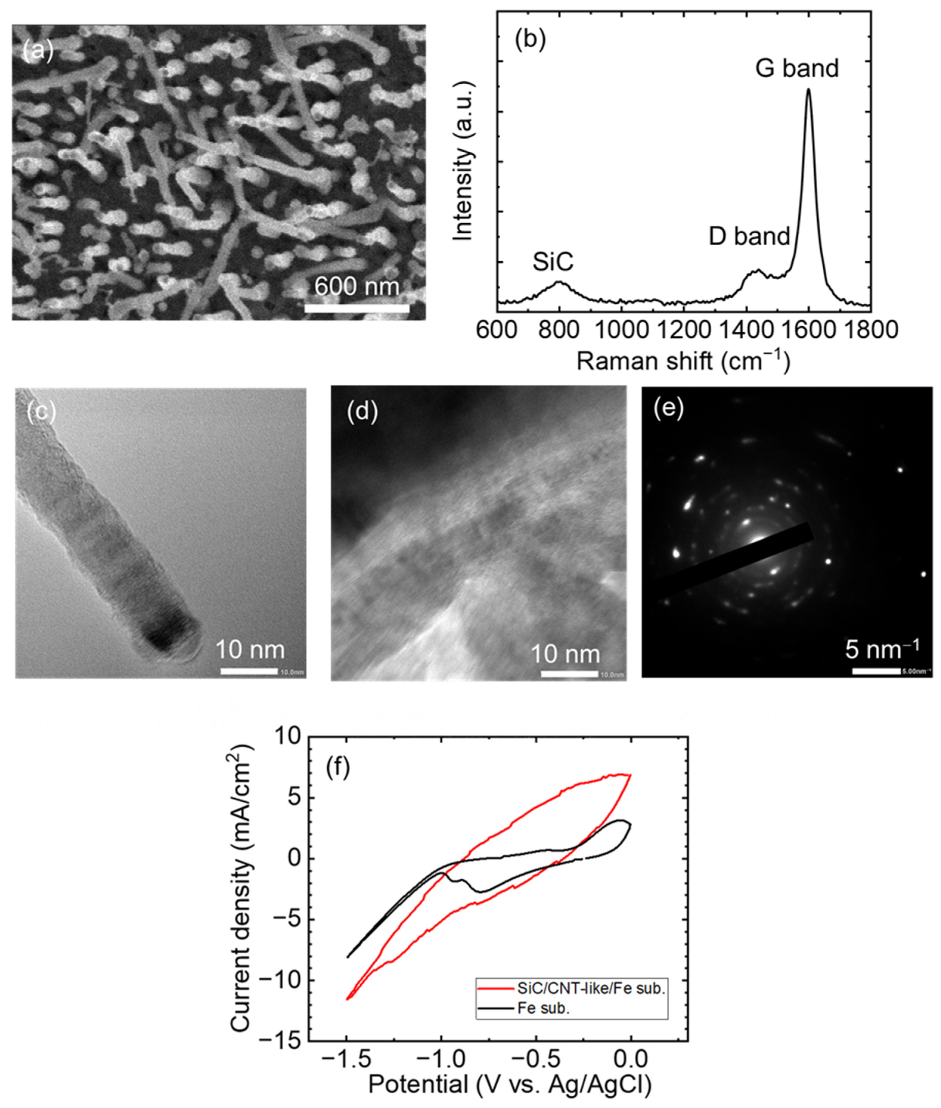
Figure 8a shows a surface SEM image of the obtained structure. Filamentous structures are observed to grow relatively straight from the surface, consistent with the formation of CNT-like filamentous structures. The coexistence of graphitic carbon and SiC was confirmed by UV Raman spectroscopy, as shown in Figure 8b. A peak near 800 cm−1 corresponds to the transverse optical (TO) phonon mode of SiC [23], while the bands around 1430 and 1580 cm−1 are attributed to disordered carbon and the G band of sp2-bonded carbon, respectively. TEM observations revealed hollow filamentous nanostructures with graphitic layered walls (Figure 8c). In addition, graphitic layered structures were observed in another region (Figure 8d), and the corresponding selected-area electron diffraction (SAED) pattern exhibited ring-like diffraction features composed of numerous diffraction spots (Figure 8e), consistent with the presence of polycrystalline graphitic domains within the deposited carbon nanostructures.
Figure 8.
Structural characterization and electrochemical performance of the SiC/CNT-like/Fe structure formed on an Fe bulk substrate using vinylsilane (850 °C, 2 sccm, 1 h). (a) Surface SEM image of the deposited structure. (b) UV Raman spectrum showing SiC- and graphitic carbon-related features. (c) TEM image showing a hollow filamentous nanostructure with graphitic layered walls. (d) TEM image showing graphitic layered structures. (e) Selected-area electron diffraction (SAED) pattern obtained from the region shown in (d). (f) Cyclic voltammetry (CV) curves measured in a 0.1 mol/L Na2SO4 aqueous electrolyte using an Ag/AgCl reference electrode and a Pt counter electrode, comparing the bare Fe substrate and the SiC/CNT-like/Fe electrode.
Figure 8f shows the cyclic voltammetry (CV) curves of the bare Fe bulk substrate and the SiC/CNT-like/Fe electrode measured in a 0.1 mol/L Na2SO4 aqueous electrolyte using an Ag/AgCl reference electrode and a Pt counter electrode. The working electrode area was 0.5 cm2, and the scan rate was 100 mV/s. The curves correspond to the 100th cycle after stabilization following initial changes during the first ~30 cycles. The bare Fe bulk substrate exhibits distinct redox peaks associated with iron oxidation–reduction reactions [43,44]. In contrast, the SiC/CNT-like/Fe electrode shows suppressed redox peaks and a broadened current response, which is consistent with a reduced contribution from iron oxidation–reduction reactions and a greater contribution from capacitive behavior. The CNT-like framework may contribute to the observed increase in current response because conductive graphitic carbon domains are present within the deposited structure. As a result, the overall current response is increased over the entire potential range. In addition, in the negative potential region, a decrease in hysteresis accompanied by an increase in cathodic current is observed, which may reflect differences in interfacial electrochemical behavior at the electrode surface. Consistent with this behavior, gas evolution was visually observed during the electrochemical measurements, which is consistent with the occurrence of electrochemical gas-evolution reactions at the electrode surface. Furthermore, owing to the intrinsically high corrosion resistance of SiC [45], the SiC component is expected to contribute to the improved chemical stability of the electrode.
4. Discussion
In this study, clear differences were observed in the formation behavior of carbon-related structures and SiC films between Fe bulk substrates and Fe thin-film substrates when vinylsilane was used as a single-source precursor. Because Fe exhibited the most pronounced filamentous morphology among the investigated metal substrates, Fe bulk and Fe thin-film substrates were selected as representative systems for discussing the growth mechanism in detail. It should be noted that the growth conditions used for bulk-metal and thin-film substrates were not identical, particularly with respect to vinylsilane flow rate and total pressure. Therefore, although the observed differences are consistent with variations in catalyst availability and Si uptake behavior, the possible contributions from differences in growth conditions cannot be completely excluded. Based on the combined results of SEM, Raman spectroscopy, XRD, and XPS, the growth mechanism can be understood in terms of (i) the available amount of Fe catalyst, (ii) diffusion/uptake behavior of Si species into Fe, and (iii) the balance between Si incorporation and surface reaction processes.
On Fe bulk substrates, vinylsilane is considered to decompose upon reaching the Fe surface into carbon-related species and Si-containing species. The generated Si species preferentially diffuse into and are incorporated into the Fe substrate, where they react with Fe to form Fe–Si phases, as supported by the XRD results. This behavior is consistent with previous studies reporting strong affinity and interdiffusion between Fe and Si at elevated temperatures [46,47]. As a result, the near-surface region becomes relatively depleted in Si and enriched in carbon. Under such conditions, Fe and/or Fe–Si silicide phases (hereafter denoted as Fe–Si phases) provide catalytic sites for the formation of sp2-bonded carbon structures, thereby favoring the formation of CNT-like filamentous carbon structures, while the formation of Si–C-rich phases is suppressed. This interpretation is supported by SEM, Raman, and XPS results showing CNT-like structures with dominant C–C/C–H bonding components.
In contrast, the growth behavior on Fe thin-film substrates differs markedly due to the limited amount of available Fe. During the initial stage of growth, CNT-like structures are formed while Si species are still able to diffuse into and be incorporated into the Fe layer. However, as growth proceeds, the capacity of the Fe layer to accommodate Si becomes limited due to progressive formation of Fe–Si phases. Under these conditions, further Si incorporation is restricted, and the balance between Si diffusion into the metal and surface reaction shifts.
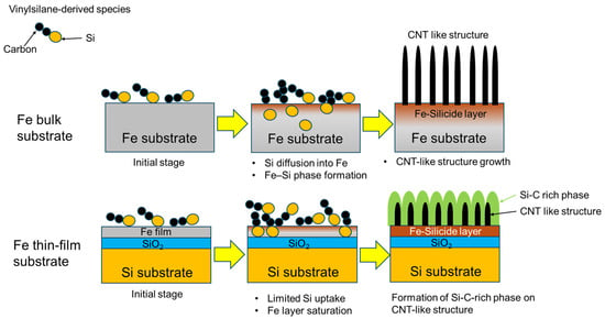
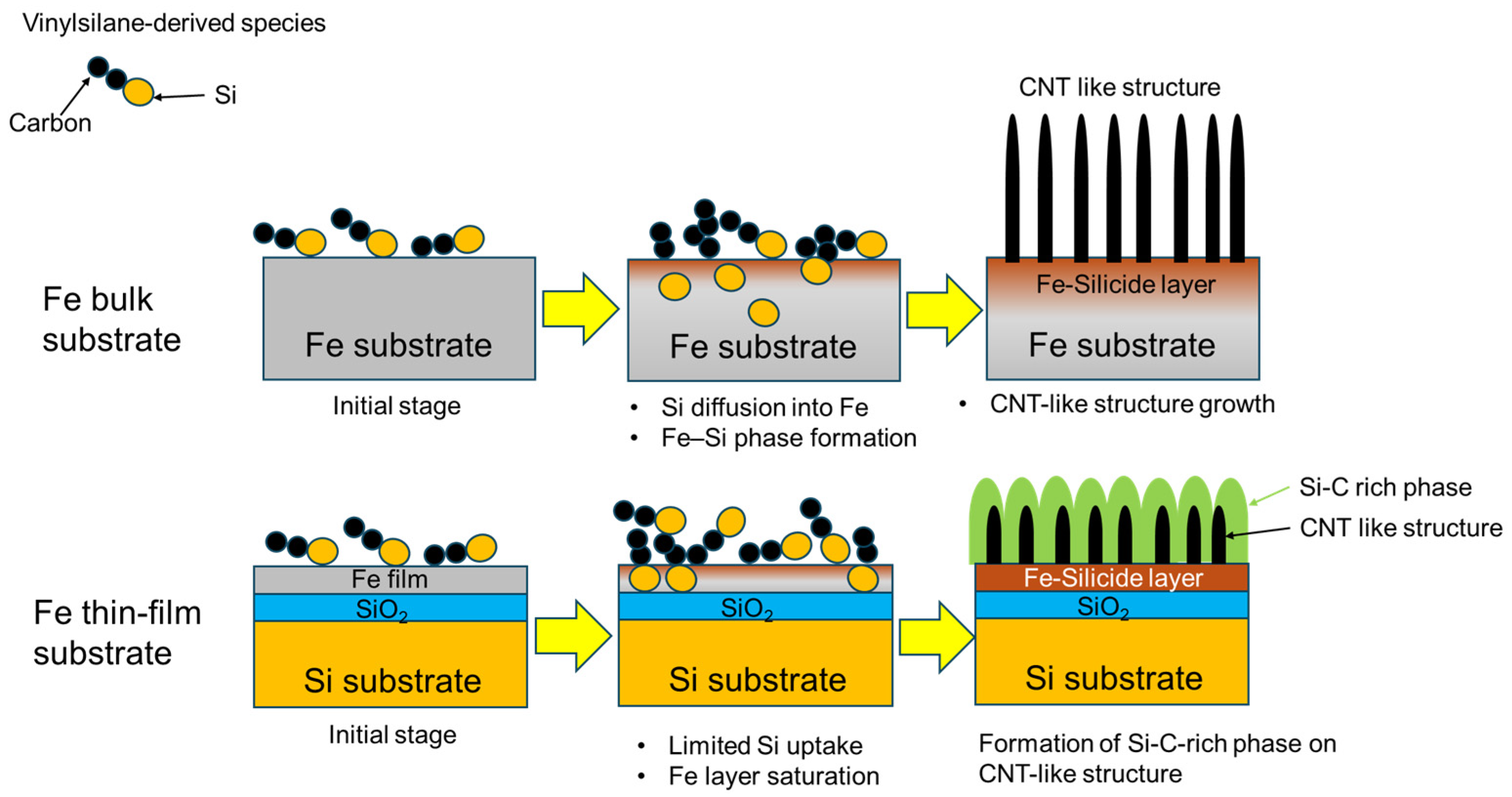
When the rate of Si–C-rich phase formation at the surface becomes comparable to or exceeds the rate of Si diffusion into the Fe layer, the growth mode transitions from CNT-like structure formation to the development of Si–C-rich coated structures. This transition is interpreted to be associated with two key factors: (1) accumulation of Si within the metal catalyst layer, and (2) the relative increase in the surface reaction rate of SiC formation, which depends on growth temperature and precursor supply. In this sense, the transition from CNT-like growth to SiC formation is unlikely to be explained solely by conventional catalyst deactivation and is interpreted to be more consistent with a diffusion/uptake-limited shift in the local reaction environment for the Fe system investigated in this study. A schematic illustration of the proposed growth mechanism is shown in Figure 9. On Fe bulk substrates, Si species generated from vinylsilane are considered to diffuse into the Fe substrate and contribute to Fe–Si silicide formation, resulting in a Si-depleted and carbon-rich surface environment because Si is considered to be continuously consumed through Fe–Si silicide formation and diffusion into the Fe substrate, thereby favoring CNT-like growth. In contrast, the limited Fe volume in Fe thin-film substrates may restrict further Si uptake, leading to saturation of the Fe layer and enhanced surface accumulation of Si-containing species. Under these conditions, Si–C-rich phases gradually develop on the pre-existing CNT-like structures, resulting in the coated morphology observed after prolonged growth.
Figure 9.
Schematic illustration of the proposed growth mechanism on Fe bulk and Fe thin-film substrates during vinylsilane decomposition. On Fe bulk substrates, continuous incorporation and diffusion of Si species into the substrate are proposed to promote Fe–Si silicide formation and maintain a relatively carbon-rich surface environment favorable for CNT-like growth. In contrast, the limited Fe volume in thin-film substrates may restrict further Si uptake, which may lead to the accumulation of Si-containing species near the surface and the subsequent formation of Si–C-rich coated structures. Yellow arrows indicate the progression of the proposed growth process. Black and orange circles represent carbon (C) and silicon (Si), respectively.
Importantly, the time-dependent growth experiments further support this interpretation. At intermediate temperatures (e.g., 850 °C), CNT-like structures are initially formed, followed by lateral thickening and the appearance of coating-like features. This behavior suggests that the balance between Si diffusion into the Fe layer and surface reaction processes evolves during growth. One possible explanation is that, as CNT-like structures grow, the effective transport of precursor species to the catalyst surface becomes limited. In addition, the accumulation of Si within the Fe layer may reduce the driving force for further Si diffusion. These effects can lead to a gradual transition from CNT-like growth to the formation of Si–C-rich coated structures during the growth process.
Such a dynamic balance between diffusion and surface reaction processes is a characteristic feature of single-source precursor systems such as vinylsilane, in which carbon and silicon species are simultaneously supplied from the same molecular precursor. As a result, the local reaction environment can shift between carbon-rich and SiC-forming conditions depending on catalyst availability and diffusion kinetics. Although detailed analysis was conducted for Fe, similar temperature-dependent trends were observed for other catalytic metals such as Ni and Co in SEM and XRD measurements, whereas no comparable behavior was observed for non-catalytic Ti. Although similar temperature-dependent morphological trends were observed for Ni and Co in SEM and XRD measurements, the present evidence is insufficient to establish the same diffusion/uptake-limited mechanism for these substrates. Therefore, the detailed mechanism proposed here should be regarded as being primarily supported by the Fe-based systems investigated in this study. In addition to the growth mechanism, the presence of CNT-like structures at the early stage may also influence the final morphology. The formation of CNT-like structures may also contribute to stress relaxation during film growth and subsequent cooling owing to their compliant filamentous morphology, which can partially accommodate thermal-expansion mismatch stresses between the deposited layer and the substrate, as suggested in related CNT-containing composite systems [15]. This effect may explain differences in particle morphology observed on metal thin-film substrates.
Furthermore, the electrochemical results suggest that this growth mechanism may be utilized to design SiC/CNT-like composite electrode structures on conductive metal substrates. The CNT-like network formed at the early stage provides a high-surface-area electrically conductive sp2-carbon framework, contributing to enhanced capacitive behavior consistent with the electric double-layer characteristics of CNT-based materials [48]. Binder-free CNT electrodes, such as free-standing CNT films, have been investigated for electrochemical applications [49]. However, many reported systems rely on additional catalysts or involve binder-assisted or multistep fabrication processes. In contrast, the present structure is directly formed on a conductive substrate through a single-step process, which may provide advantages in electrical contact, structural integration, and fabrication simplicity. The subsequent formation of SiC plays a complementary role by improving the structural and chemical stability of the system. SiC is known for its excellent oxidation resistance and chemical stability [45], and SiC/CNT composite materials have traditionally been developed for applications requiring high thermal stability and mechanical robustness [50]. Here, this combination is achieved through a single-step process, in contrast to conventional multistep approaches involving CNT growth followed by SiC deposition at higher temperatures [50]. The integration of CNT-like carbon structures as conductive frameworks and SiC as a chemically stable component suggests that the SiC/CNT-like/Fe structure may be a promising platform for future electrochemical applications. Although quantitative evaluation of water electrolysis performance was not conducted, gas evolution was visually observed during electrochemical measurements, which is consistent with the occurrence of electrochemical gas-evolution reactions at the electrode surface, although dedicated water-electrolysis performance measurements were beyond the scope of the present study. Furthermore, the observed characteristics, including suppressed Fe-related redox features and increased current response, suggest that the SiC/CNT-like/Fe structure may be of interest for future electrochemical applications. However, a comprehensive evaluation of electrocatalytic performance was beyond the scope of the present study.
Therefore, the present study not only clarifies the growth mechanism of CNT-like structures and SiC formation using a single-source precursor but also suggests a possible strategy for designing integrated, binder-free electrode structures based on controlled competition between diffusion and surface reaction processes.
5. Conclusions
In this study, the growth behavior of carbon-related structures and SiC films using vinylsilane as a single-source precursor was systematically investigated on various substrates, with particular focus on the differences between Fe bulk substrates and Fe thin-film substrates. Substrate-dependent growth behavior was observed through SEM, Raman spectroscopy, XRD, and XPS analyses.
On non-catalytic substrates such as SiO2 and Ti, SiC formation predominated, as evidenced by Raman spectroscopy, indicating the formation of SiC-based films containing amorphous carbon depending on the growth temperature. In contrast, Fe bulk substrates were associated with the formation of CNT-like structures, which is consistent with preferential incorporation of Si into the Fe substrate and the development of relatively carbon-rich surface conditions. When Fe thin-film substrates were used, the limited catalyst amount was associated with a transition from CNT-like growth to SiC-related phase formation as growth temperature and growth time increased. At elevated temperatures, crystalline SiC, including polycrystalline 3C-SiC, was observed on several metal thin-film substrates, suggesting an increased contribution of SiC formation under conditions where surface reaction processes are favored. These results indicate that the relative formation of CNT-like structures and SiC-related phases can be influenced by the catalyst amount, growth temperature, and growth time. In particular, the observed growth transition is interpreted as being consistent with a competition between Si diffusion/uptake into the metal and surface SiC formation processes.
Furthermore, the present study shows that SiC/CNT-like composite structures can be directly formed on conductive Fe substrates in a single-step process. The resulting structures showed an enhanced current response compared with a bare Fe substrate, indicating preliminary electrochemical activity and suggesting potential applicability as high-surface-area electrode materials.
Overall, this work provides insight into growth control using vinylsilane as a single-source precursor and suggests that catalyst amount and Si uptake behavior appear to play important roles in determining the balance between CNT-like structure formation and SiC-related phase formation.
Supplementary Materials
The following supporting information can be downloaded at: https://www.mdpi.com/article/10.3390/appliedphys2030007/s1, Table S1. Raman fitting parameters (peak position, FWHM, IG/ID, and I2D/IG) for carbon-related structures formed on different substrates after growth using vinylsilane as a single-source precursor; Table S2. XPS peak fitting parameters for Fe bulk and Fe thin-film samples grown at 950 °C.
Author Contributions
Conceptualization, W.T.; methodology, W.T., Y.T. and K.O.; validation, W.T., Y.T. and K.O.; formal analysis, W.T., Y.T. and K.O.; investigation, W.T., Y.T., K.O. and K.U.; resources, W.T., K.U. and S.Y.; data curation, Y.T. and K.O.; writing—original draft preparation, W.T.; writing—review and editing, W.T., D.O. and K.E.; visualization, W.T., Y.T. and K.O.; supervision, W.T., D.O. and K.E.; project administration, W.T.; funding acquisition, W.T. and S.Y. All authors have read and agreed to the published version of the manuscript.
Funding
This research was supported by the Kanagawa Institute of Industrial Science and Technology (KISTEC).
Data Availability Statement
The data presented in this study are available from the corresponding author upon reasonable request.
Acknowledgments
This work was carried out by the joint usage/research program of the Center for Low temperature Plasma Sciences, Nagoya University and Advanced Research Infrastructure for Materials and Nanotechnology in Japan (ARIM). The authors gratefully acknowledge Hiroyuki Iwata of Aichi Institute of Technology for his assistance with transmission electron microscopy (TEM) observations. During the preparation of this manuscript, the authors used ChatGPT (OpenAI) for language editing and text refinement. The authors have reviewed and edited the content and take full responsibility for the scientific accuracy and integrity of this work.
Conflicts of Interest
Authors Kenichi Uehara and Shigeo Yasuhara were employed by the company Japan Advanced Chemicals Ltd. The remaining authors declare that the research was conducted in the absence of any commercial or financial relationships that could be construed as a potential conflict of interest.
References
- Kaloyeros, A.E.; Arkles, B. Silicon Carbide Thin Film Technologies: Recent Advances in Processing, Properties, and Applications—Part I Thermal and Plasma CVD. ECS J. Solid State Sci. Technol. 2023, 12, 103001. [Google Scholar] [CrossRef] [Scilit]
- Schwarz, C.; Heeg, J.; Rosenberg, M.; Wienecke, M. Investigation on wear and adhesion of graded Si/SiC/DLC coatings deposited by plasma-enhanced-CVD. Diam. Relat. Mater. 2008, 17, 1685–1688. [Google Scholar] [CrossRef] [Scilit]
- Guruvenket, S.; Azzi, M.; Li, D.; Szpunar, J.A.; Martinu, L.; Klemberg-Sapieha, J.E. Structural, mechanical, tribological, and corrosion properties of a-SiC:H coatings prepared by PECVD. Surf. Coat. Technol. 2010, 204, 3358–3365. [Google Scholar] [CrossRef] [Scilit]
- Ordine, A.; Achete, C.A.; Mattos, O.R.; Margarit, I.C.P.; Camargo, S.S., Jr.; Hirsch, T. Magnetron sputtered SiC coatings as corrosion protection barriers for steels. Surf. Coat. Technol. 2000, 133–134, 583–588. [Google Scholar] [CrossRef] [Scilit]
- Jian, J.; Sun, J. A Review of Recent Progress on Silicon Carbide for Photoelectrochemical Water Splitting. Sol. RRL 2020, 4, 2000111. [Google Scholar] [CrossRef] [Scilit]
- Meyyappan, M.; Delzeit, L.; Cassell, A.; Hash, D. Carbon nanotube growth by PECVD: A review. Plasma Sources Sci. Technol. 2003, 12, 205–216. [Google Scholar] [CrossRef] [Scilit]
- Kumar, M.; Ando, Y. Chemical Vapor Deposition of Carbon Nanotubes: A Review on Growth Mechanism and Mass Production. J. Nanosci. Nanotechnol. 2010, 10, 3739–3758. [Google Scholar] [CrossRef] [Scilit] [PubMed]
- Ahmad, M.; Silva, S.R.P. Low temperature growth of carbon nanotubes—A review. Carbon 2020, 158, 24–44. [Google Scholar] [CrossRef] [Scilit]
- Rai, S.; Ikram, A.; Sahai, S.; Dass, S.; Shrivastav, R.; Satsangi, V.R. CNT based photoelectrodes for PEC generation of hydrogen: A review. Int. J. Hydrogen Energy 2017, 42, 3994–4006. [Google Scholar] [CrossRef] [Scilit]
- Digdya, I.A.; Han, L.; Buijs, T.W.F.; Zeman, M.; Dam, B.; Smets, A.H.M.; Smith, W.A. Extracting Large Photovoltages from a-SiC Photocathodes with an Amorphous TiO2 Front Surface Field Layer for Solar Hydrogen Evolution. Energy Environ. Sci. 2015, 8, 3557–3568. [Google Scholar] [CrossRef] [Scilit]
- Zhu, F.; Hu, J.; Matulionis, I.; Deutsch, T.; Gaillard, N.; Kunrath, A.; Miller, E.; Madan, A. Amorphous silicon carbide photoelectrode for hydrogen production directly from water using sunlight. Philos. Mag. 2009, 89, 2723–2739. [Google Scholar] [CrossRef] [Scilit]
- Ichikawa, N.; Kato, M.; Ichimura, M. The enhanced performance of 3C-SiC photocathodes for the generation of hydrogen through the use of cocatalysts. Appl. Phys. Lett. 2016, 109, 153904. [Google Scholar] [CrossRef] [Scilit]
- Yasuda, T.; Kato, M.; Ichimura, M.; Hatayama, T. SiC photoelectrodes for a self-driven water-splitting cell. Appl. Phys. Lett. 2012, 101, 053902. [Google Scholar] [CrossRef] [Scilit]
- Gu, Z.; Yang, Y.; Li, K.; Tao, X.; Eres, G.; Howe, J.Y.; Zhang, L.; Li, X.; Pan, Z. Aligned carbon nanotube-reinforced silicon carbide composites produced by chemical vapor infiltration. Carbon 2011, 49, 2475–2482. [Google Scholar] [CrossRef] [Scilit]
- Feng, L.; Li, K.; Si, Z.; Li, H.; Song, Q.; Shan, Y.; Wen, S. Microstructure and thermal shock resistance of SiC/CNT–SiC double-layer coating for carbon/carbon composites. Ceram. Int. 2014, 40, 13683–13689. [Google Scholar] [CrossRef] [Scilit]
- Chen, S.; Feng, Y.; Qin, M.; Ji, T.; Feng, W. Improving thermal conductivity in the through-thickness direction of carbon fibre/SiC composites by growing vertically aligned carbon nanotubes. Carbon 2017, 116, 84–93. [Google Scholar] [CrossRef] [Scilit]
- Jiang, G.; Chen, L.; Zhang, S.; Huang, H. Superhydrophobic SiC/CNTs coatings with photothermal deicing and passive anti-icing properties. ACS Appl. Mater. Interfaces 2018, 10, 36505–36511. [Google Scholar] [CrossRef] [Scilit] [PubMed]
- Doi, T.; Takeuchi, W.; Jin, Y.; Kokubun, H.; Yasuhara, S.; Nakatsuka, O.; Zaima, S. Formation of SiC thin films by chemical vapor deposition with vinylsilane precursor. Jpn. J. Appl. Phys. 2018, 57, 01AE08. [Google Scholar] [CrossRef] [Scilit]
- Doi, T.; Hashimoto, K.; Takeuchi, W.; Nakatsuka, O. Crystal growth of epitaxial 3C-SiC thin film on Si substrate by chemical vapor deposition using single precursor of vinylsilane. ECS Trans. 2020, 98, 169–176. [Google Scholar] [CrossRef] [Scilit]
- Ono, K.; Koide, T.; Ishikawa, K.; Tanaka, H.; Kondo, H.; Sugawara-Narutaki, A.; Jin, Y.; Yasuhara, S.; Hori, M.; Takeuchi, W. Biocompatibility of conformal silicon carbide on carbon nanowall scaffolds. Jpn. J. Appl. Phys. 2023, 62, SA1017. [Google Scholar] [CrossRef] [Scilit]
- Haddad-Adel, A.; Inokuma, T.; Kurata, Y.; Hasegawa, S. Optical and structural properties of polycrystalline 3C-SiC films. Appl. Phys. Lett. 2006, 89, 181904. [Google Scholar] [CrossRef] [Scilit]
- Jeong, J.; Jang, K.; Lee, H.S.; Chung, G.-S.; Kim, G.-Y. Raman scattering studies of polycrystalline 3C-SiC deposited on SiO2 and AlN thin films. Phys. B 2009, 404, 7–10. [Google Scholar] [CrossRef] [Scilit]
- Wang, B.; Yin, J.; Dai, D.; Long, X.; Li, L.; Lin, H.-H.; Hu, W.; Talwar, D.N.; Jia, R.-X.; Zhang, Y.-M.; et al. Optical and Surface Properties of 3C-SiC Thin Epitaxial Films Grown at Different Temperatures on 4H-SiC Substrates. Superlattices Microstruct. 2021, 156, 106960. [Google Scholar] [CrossRef] [Scilit]
- Compagnini, G.; Foti, G. 1430 cm−1 Raman line in ion implanted carbon rich amorphous silicon carbide. Nucl. Instrum. Methods Phys. Res. B 1997, 127–128, 639–642. [Google Scholar] [CrossRef] [Scilit]
- Musumeci, P.; Roccaforte, F.; Reitano, R. Angular distortion of Si clusters in a-SiC. Europhys. Lett. 2001, 55, 674–680. [Google Scholar] [CrossRef] [Scilit]
- Ferrari, A.C.; Robertson, J. Interpretation of Raman spectra of disordered and amorphous carbon. Phys. Rev. B 2000, 61, 14095–14107. [Google Scholar] [CrossRef] [Scilit]
- Dresselhaus, M.S.; Jorio, A.; Hofmann, M.; Dresselhaus, G.; Saito, R. Perspectives on carbon nanotubes and graphene Raman spectroscopy. Nano Lett. 2010, 10, 751–758. [Google Scholar] [CrossRef] [Scilit] [PubMed]
- Jorio, A.; Saito, R. Raman spectroscopy for carbon nanotube applications. J. Appl. Phys. 2021, 129, 021102. [Google Scholar] [CrossRef] [Scilit]
- Reich, S.; Thomsen, C. Raman spectroscopy of graphite. Philos. Trans. A Math. Phys. Eng. Sci. 2004, 362, 2271–2288. [Google Scholar] [CrossRef] [Scilit] [PubMed]
- Dresselhaus, M.S.; Jorio, A.; Saito, R. Characterizing graphene, graphite, and carbon nanotubes by Raman spectroscopy. Annu. Rev. Condens. Matter Phys. 2010, 1, 89–108. [Google Scholar] [CrossRef] [Scilit]
- Zólyomi, V.; Koltai, J.; Kürti, J. Resonance Raman spectroscopy of graphite and graphene. Phys. Status Solidi B 2011, 248, 2435–2444. [Google Scholar] [CrossRef] [Scilit]
- Cao, A.; Xu, C.; Liang, J.; Wu, D.; Wei, B. X-ray diffraction characterization on the alignment degree of carbon nanotubes. Chem. Phys. Lett. 2001, 344, 13–17. [Google Scholar] [CrossRef] [Scilit]
- Singh, D.K.; Iyer, P.K.; Giri, P.K. Diameter dependence of interwall separation and strain in multiwalled carbon nanotubes probed by X-ray diffraction and Raman scattering studies. Diam. Relat. Mater. 2010, 19, 1281–1288. [Google Scholar] [CrossRef] [Scilit]
- Li, Z.Q.; Lu, C.J.; Xia, Z.P.; Zhou, Y.; Luo, Z. X-ray diffraction patterns of graphite and turbostratic carbon. Carbon 2007, 45, 1686–1695. [Google Scholar] [CrossRef] [Scilit]
- Milev, A.; Wilson, M.; Kannangara, G.S.K.; Tran, N. X-ray diffraction line profile analysis of nanocrystalline graphite. Mater. Chem. Phys. 2008, 111, 346–350. [Google Scholar] [CrossRef] [Scilit]
- Cheng, F.; Jiang, C.; Wu, J. Study of crystallization and phase transformation in amorphous Co–Si thin film by X-ray diffraction. Mater. Trans. 2004, 45, 2471–2473. [Google Scholar] [CrossRef] [Scilit]
- Shyni, P.C.; Alagarsamy, P. Thermomagnetic properties of nanocrystalline Fe–Si alloys with high Si content. Phys. B Condens. Matter 2014, 448, 60–63. [Google Scholar] [CrossRef] [Scilit]
- Forbes, A.W.; Dulal, R.P.; Bhattarai, N.; Pegg, I.L.; Philip, J. Experimental realization and magnetotransport properties of half-metallic Fe2Si. J. Appl. Phys. 2019, 125, 243902. [Google Scholar] [CrossRef] [Scilit]
- Iwanowski, R.J.; Fronc, K.; Paszkowicz, W.; Heinonen, M. XPS and XRD study of crystalline 3C-SiC grown by sublimation method. J. Alloys Compd. 1999, 286, 143–147. [Google Scholar] [CrossRef] [Scilit]
- Roper, C.S.; Radmilovic, V.; Howe, R.T.; Maboudian, R. Characterization of polycrystalline 3C-SiC films deposited from the precursors 1,3-disilabutane and dichlorosilane. J. Appl. Phys. 2008, 103, 084907. [Google Scholar] [CrossRef] [Scilit]
- Al-Joubouri, A.A.; Suryanarayana, C. Synthesis of stable and metastable phases in the Ni–Si system by mechanical alloying. Powder Technol. 2016, 302, 8–14. [Google Scholar] [CrossRef] [Scilit]
- Choi, W.K.; Ong, T.Y.; Tan, L.S.; Loh, F.C.; Tan, K.L. Infrared and X-ray photoelectron spectroscopy studies of as-prepared and furnace-annealed radio-frequency sputtered amorphous silicon carbide films. J. Appl. Phys. 1998, 83, 4968–4974. [Google Scholar] [CrossRef] [Scilit]
- Bülter, H.; Denuault, G.; Mátéfi-Tempfli, S.; Mátéfi-Tempfli, M.; Dostálek, J.; Wittstock, G. Electrochemical Analysis of Nanostructured Iron Oxides Using Cyclic Voltammetry and Scanning Electrochemical Microscopy. Electrochim. Acta 2016, 222, 1326–1334. [Google Scholar] [CrossRef] [Scilit]
- Xu, Q.; Zhao, T.S.; Wei, L.; Zhang, C.; Zhou, X.L. Electrochemical Characteristics and Transport Properties of Fe(II)/Fe(III) Redox Couple in a Non-Aqueous Reline Deep Eutectic Solvent. Electrochim. Acta 2015, 154, 462–467. [Google Scholar] [CrossRef] [Scilit]
- Chen, D.; Zhang, H.; Zhang, G.; Zhao, G.; Zhu, Z.; Yang, J.; He, J.; Li, J.; Yu, Z.; Zhu, Z. Investigating the Corrosion Resistance of Different SiC Crystal Types: From Energy Sectors to Advanced Applications. Langmuir 2024, 40, 12322–12342. [Google Scholar] [CrossRef] [Scilit] [PubMed]
- Vinh, L.T.; Chevrier, J.; Derrien, J. Epitaxial growth of Fe–Si compounds on the silicon (111) face. Phys. Rev. B 1992, 46, 15946–15953. [Google Scholar] [CrossRef] [Scilit] [PubMed]
- Oh, J.H.; Lee, S.K.; Han, K.P.; An, K.S.; Park, C.Y. Effects of the different heat treatments on the growth and formation of iron silicide on Si(100). Thin Solid Films 1999, 341, 160–164. [Google Scholar] [CrossRef] [Scilit]
- Frackowiak, E.; Béguin, F. Carbon Materials for the Electrochemical Storage of Energy in Capacitors. Carbon 2001, 39, 937–950. [Google Scholar] [CrossRef] [Scilit]
- Kordek-Khalil, K.; Janas, D.; Rutkowski, P. Revealing the effect of electrocatalytic performance boost during hydrogen evolution reaction on free-standing SWCNT film electrode. Sci. Rep. 2021, 11, 19981. [Google Scholar] [CrossRef] [Scilit] [PubMed]
- Cai, J.; Ma, D.; Peng, Y.; Li, Z.; Miao, M.; Fan, B.; Feng, X.; Li, A. Uniform Carbon Nanotube Growth on Carbon Felt Preforms: Enhancing Mechanical and Electromagnetic Shielding Properties of C/SiC Composites. Compos. Commun. 2025, 56, 102403. [Google Scholar] [CrossRef] [Scilit]

Disclaimer/Publisher’s Note: The statements, opinions and data contained in all publications are solely those of the individual author(s) and contributor(s) and not of MDPI and/or the editor(s). MDPI and/or the editor(s) disclaim responsibility for any injury to people or property resulting from any ideas, methods, instructions or products referred to in the content. |
© 2026 by the authors. Licensee MDPI, Basel, Switzerland. This article is an open access article distributed under the terms and conditions of the Creative Commons Attribution (CC BY) license.